WO2007114143A1 - 薄膜センサの製造方法、薄膜センサおよび薄膜センサモジュール - Google Patents
薄膜センサの製造方法、薄膜センサおよび薄膜センサモジュール Download PDFInfo
- Publication number
- WO2007114143A1 WO2007114143A1 PCT/JP2007/056589 JP2007056589W WO2007114143A1 WO 2007114143 A1 WO2007114143 A1 WO 2007114143A1 JP 2007056589 W JP2007056589 W JP 2007056589W WO 2007114143 A1 WO2007114143 A1 WO 2007114143A1
- Authority
- WO
- WIPO (PCT)
- Prior art keywords
- thin film
- film sensor
- sensor
- insulating substrate
- metal
- Prior art date
Links
- 239000010409 thin film Substances 0.000 title claims abstract description 129
- 238000000034 method Methods 0.000 title claims abstract description 30
- 239000013078 crystal Substances 0.000 claims abstract description 54
- 239000000758 substrate Substances 0.000 claims abstract description 42
- 229910052751 metal Inorganic materials 0.000 claims abstract description 20
- 239000002184 metal Substances 0.000 claims abstract description 20
- 238000004544 sputter deposition Methods 0.000 claims abstract description 13
- BASFCYQUMIYNBI-UHFFFAOYSA-N platinum Chemical compound [Pt] BASFCYQUMIYNBI-UHFFFAOYSA-N 0.000 claims description 39
- 239000000463 material Substances 0.000 claims description 29
- 238000004519 manufacturing process Methods 0.000 claims description 24
- 229910052697 platinum Inorganic materials 0.000 claims description 18
- 150000001875 compounds Chemical class 0.000 claims description 11
- QVGXLLKOCUKJST-UHFFFAOYSA-N atomic oxygen Chemical compound [O] QVGXLLKOCUKJST-UHFFFAOYSA-N 0.000 claims description 9
- 239000001301 oxygen Substances 0.000 claims description 9
- 229910052760 oxygen Inorganic materials 0.000 claims description 9
- 230000003746 surface roughness Effects 0.000 claims description 9
- 229910052723 transition metal Inorganic materials 0.000 claims description 8
- 150000003624 transition metals Chemical class 0.000 claims description 8
- IJGRMHOSHXDMSA-UHFFFAOYSA-N Atomic nitrogen Chemical compound N#N IJGRMHOSHXDMSA-UHFFFAOYSA-N 0.000 claims description 6
- KDLHZDBZIXYQEI-UHFFFAOYSA-N Palladium Chemical compound [Pd] KDLHZDBZIXYQEI-UHFFFAOYSA-N 0.000 claims description 6
- 239000007788 liquid Substances 0.000 claims description 6
- OKTJSMMVPCPJKN-UHFFFAOYSA-N Carbon Chemical compound [C] OKTJSMMVPCPJKN-UHFFFAOYSA-N 0.000 claims description 5
- 229910052799 carbon Inorganic materials 0.000 claims description 5
- PXGOKWXKJXAPGV-UHFFFAOYSA-N Fluorine Chemical compound FF PXGOKWXKJXAPGV-UHFFFAOYSA-N 0.000 claims description 3
- KJTLSVCANCCWHF-UHFFFAOYSA-N Ruthenium Chemical compound [Ru] KJTLSVCANCCWHF-UHFFFAOYSA-N 0.000 claims description 3
- 239000011737 fluorine Substances 0.000 claims description 3
- 229910052731 fluorine Inorganic materials 0.000 claims description 3
- 229910052741 iridium Inorganic materials 0.000 claims description 3
- GKOZUEZYRPOHIO-UHFFFAOYSA-N iridium atom Chemical compound [Ir] GKOZUEZYRPOHIO-UHFFFAOYSA-N 0.000 claims description 3
- 229910052757 nitrogen Inorganic materials 0.000 claims description 3
- 229910052762 osmium Inorganic materials 0.000 claims description 3
- SYQBFIAQOQZEGI-UHFFFAOYSA-N osmium atom Chemical compound [Os] SYQBFIAQOQZEGI-UHFFFAOYSA-N 0.000 claims description 3
- 229910052763 palladium Inorganic materials 0.000 claims description 3
- 229910052703 rhodium Inorganic materials 0.000 claims description 3
- 239000010948 rhodium Substances 0.000 claims description 3
- MHOVAHRLVXNVSD-UHFFFAOYSA-N rhodium atom Chemical compound [Rh] MHOVAHRLVXNVSD-UHFFFAOYSA-N 0.000 claims description 3
- 229910052707 ruthenium Inorganic materials 0.000 claims description 3
- 238000010438 heat treatment Methods 0.000 abstract description 4
- 239000010410 layer Substances 0.000 description 37
- 239000010408 film Substances 0.000 description 17
- 238000000151 deposition Methods 0.000 description 15
- 230000008021 deposition Effects 0.000 description 15
- 239000010936 titanium Substances 0.000 description 14
- 238000001887 electron backscatter diffraction Methods 0.000 description 13
- RTAQQCXQSZGOHL-UHFFFAOYSA-N Titanium Chemical compound [Ti] RTAQQCXQSZGOHL-UHFFFAOYSA-N 0.000 description 11
- 229910052719 titanium Inorganic materials 0.000 description 11
- 238000004458 analytical method Methods 0.000 description 8
- PCHJSUWPFVWCPO-UHFFFAOYSA-N gold Chemical compound [Au] PCHJSUWPFVWCPO-UHFFFAOYSA-N 0.000 description 8
- 230000035945 sensitivity Effects 0.000 description 7
- 238000000137 annealing Methods 0.000 description 6
- 239000010931 gold Substances 0.000 description 6
- 238000005259 measurement Methods 0.000 description 6
- 238000011156 evaluation Methods 0.000 description 5
- 239000007789 gas Substances 0.000 description 5
- 229910052737 gold Inorganic materials 0.000 description 5
- 230000015572 biosynthetic process Effects 0.000 description 4
- 230000000052 comparative effect Effects 0.000 description 4
- 230000007423 decrease Effects 0.000 description 4
- 238000003475 lamination Methods 0.000 description 4
- 230000001681 protective effect Effects 0.000 description 4
- 150000003377 silicon compounds Chemical class 0.000 description 4
- 238000007740 vapor deposition Methods 0.000 description 4
- RYGMFSIKBFXOCR-UHFFFAOYSA-N Copper Chemical compound [Cu] RYGMFSIKBFXOCR-UHFFFAOYSA-N 0.000 description 3
- 239000012790 adhesive layer Substances 0.000 description 3
- PNEYBMLMFCGWSK-UHFFFAOYSA-N aluminium oxide Inorganic materials [O-2].[O-2].[O-2].[Al+3].[Al+3] PNEYBMLMFCGWSK-UHFFFAOYSA-N 0.000 description 3
- 230000008859 change Effects 0.000 description 3
- 239000011651 chromium Substances 0.000 description 3
- 229910052802 copper Inorganic materials 0.000 description 3
- 239000010949 copper Substances 0.000 description 3
- 239000012530 fluid Substances 0.000 description 3
- 238000001755 magnetron sputter deposition Methods 0.000 description 3
- 150000002739 metals Chemical class 0.000 description 3
- 239000002994 raw material Substances 0.000 description 3
- 238000004528 spin coating Methods 0.000 description 3
- XKRFYHLGVUSROY-UHFFFAOYSA-N Argon Chemical compound [Ar] XKRFYHLGVUSROY-UHFFFAOYSA-N 0.000 description 2
- VYZAMTAEIAYCRO-UHFFFAOYSA-N Chromium Chemical compound [Cr] VYZAMTAEIAYCRO-UHFFFAOYSA-N 0.000 description 2
- XEEYBQQBJWHFJM-UHFFFAOYSA-N Iron Chemical compound [Fe] XEEYBQQBJWHFJM-UHFFFAOYSA-N 0.000 description 2
- 239000004734 Polyphenylene sulfide Substances 0.000 description 2
- 229910052782 aluminium Inorganic materials 0.000 description 2
- XAGFODPZIPBFFR-UHFFFAOYSA-N aluminium Chemical compound [Al] XAGFODPZIPBFFR-UHFFFAOYSA-N 0.000 description 2
- 229910052804 chromium Inorganic materials 0.000 description 2
- 239000011248 coating agent Substances 0.000 description 2
- 238000000576 coating method Methods 0.000 description 2
- 238000001514 detection method Methods 0.000 description 2
- 238000005530 etching Methods 0.000 description 2
- 239000012535 impurity Substances 0.000 description 2
- 239000011261 inert gas Substances 0.000 description 2
- 238000010884 ion-beam technique Methods 0.000 description 2
- 239000002245 particle Substances 0.000 description 2
- 229920001707 polybutylene terephthalate Polymers 0.000 description 2
- 229920000069 polyphenylene sulfide Polymers 0.000 description 2
- 238000003825 pressing Methods 0.000 description 2
- 238000001552 radio frequency sputter deposition Methods 0.000 description 2
- 229920005989 resin Polymers 0.000 description 2
- 239000011347 resin Substances 0.000 description 2
- 238000010998 test method Methods 0.000 description 2
- 239000010938 white gold Substances 0.000 description 2
- 229910000832 white gold Inorganic materials 0.000 description 2
- 235000013162 Cocos nucifera Nutrition 0.000 description 1
- 244000060011 Cocos nucifera Species 0.000 description 1
- MYMOFIZGZYHOMD-UHFFFAOYSA-N Dioxygen Chemical compound O=O MYMOFIZGZYHOMD-UHFFFAOYSA-N 0.000 description 1
- 229910000737 Duralumin Inorganic materials 0.000 description 1
- 229910020177 SiOF Inorganic materials 0.000 description 1
- BQCADISMDOOEFD-UHFFFAOYSA-N Silver Chemical compound [Ag] BQCADISMDOOEFD-UHFFFAOYSA-N 0.000 description 1
- 229910001080 W alloy Inorganic materials 0.000 description 1
- QXZUUHYBWMWJHK-UHFFFAOYSA-N [Co].[Ni] Chemical compound [Co].[Ni] QXZUUHYBWMWJHK-UHFFFAOYSA-N 0.000 description 1
- 239000000956 alloy Substances 0.000 description 1
- 229910045601 alloy Inorganic materials 0.000 description 1
- 229910052786 argon Inorganic materials 0.000 description 1
- 230000005540 biological transmission Effects 0.000 description 1
- 238000004364 calculation method Methods 0.000 description 1
- 238000005229 chemical vapour deposition Methods 0.000 description 1
- 239000004020 conductor Substances 0.000 description 1
- SBYXRAKIOMOBFF-UHFFFAOYSA-N copper tungsten Chemical compound [Cu].[W] SBYXRAKIOMOBFF-UHFFFAOYSA-N 0.000 description 1
- 230000003247 decreasing effect Effects 0.000 description 1
- 230000007547 defect Effects 0.000 description 1
- 238000011161 development Methods 0.000 description 1
- 238000009792 diffusion process Methods 0.000 description 1
- 229910001882 dioxygen Inorganic materials 0.000 description 1
- KPUWHANPEXNPJT-UHFFFAOYSA-N disiloxane Chemical class [SiH3]O[SiH3] KPUWHANPEXNPJT-UHFFFAOYSA-N 0.000 description 1
- 238000009826 distribution Methods 0.000 description 1
- 238000010292 electrical insulation Methods 0.000 description 1
- 239000003822 epoxy resin Substances 0.000 description 1
- 239000010419 fine particle Substances 0.000 description 1
- 239000011521 glass Substances 0.000 description 1
- 230000006872 improvement Effects 0.000 description 1
- 229910010272 inorganic material Inorganic materials 0.000 description 1
- 239000011147 inorganic material Substances 0.000 description 1
- 239000011810 insulating material Substances 0.000 description 1
- 229910052742 iron Inorganic materials 0.000 description 1
- 230000007246 mechanism Effects 0.000 description 1
- 239000012528 membrane Substances 0.000 description 1
- 238000002156 mixing Methods 0.000 description 1
- 238000012986 modification Methods 0.000 description 1
- 230000004048 modification Effects 0.000 description 1
- 238000000465 moulding Methods 0.000 description 1
- 239000003921 oil Substances 0.000 description 1
- 230000003287 optical effect Effects 0.000 description 1
- 238000000059 patterning Methods 0.000 description 1
- 230000000704 physical effect Effects 0.000 description 1
- 238000007747 plating Methods 0.000 description 1
- 238000005498 polishing Methods 0.000 description 1
- -1 polybutylene terephthalate Polymers 0.000 description 1
- 229920000647 polyepoxide Polymers 0.000 description 1
- 230000008569 process Effects 0.000 description 1
- 230000004044 response Effects 0.000 description 1
- 229910052710 silicon Inorganic materials 0.000 description 1
- 239000010703 silicon Substances 0.000 description 1
- 229910052814 silicon oxide Inorganic materials 0.000 description 1
- 229910052709 silver Inorganic materials 0.000 description 1
- 239000004332 silver Substances 0.000 description 1
- 238000009751 slip forming Methods 0.000 description 1
- 238000003980 solgel method Methods 0.000 description 1
- 238000010972 statistical evaluation Methods 0.000 description 1
- 238000012916 structural analysis Methods 0.000 description 1
- 239000000126 substance Substances 0.000 description 1
- WFKWXMTUELFFGS-UHFFFAOYSA-N tungsten Chemical compound [W] WFKWXMTUELFFGS-UHFFFAOYSA-N 0.000 description 1
- 229910052721 tungsten Inorganic materials 0.000 description 1
- 239000010937 tungsten Substances 0.000 description 1
Classifications
-
- H—ELECTRICITY
- H01—ELECTRIC ELEMENTS
- H01C—RESISTORS
- H01C17/00—Apparatus or processes specially adapted for manufacturing resistors
- H01C17/06—Apparatus or processes specially adapted for manufacturing resistors adapted for coating resistive material on a base
- H01C17/075—Apparatus or processes specially adapted for manufacturing resistors adapted for coating resistive material on a base by thin film techniques
- H01C17/12—Apparatus or processes specially adapted for manufacturing resistors adapted for coating resistive material on a base by thin film techniques by sputtering
-
- G—PHYSICS
- G01—MEASURING; TESTING
- G01J—MEASUREMENT OF INTENSITY, VELOCITY, SPECTRAL CONTENT, POLARISATION, PHASE OR PULSE CHARACTERISTICS OF INFRARED, VISIBLE OR ULTRAVIOLET LIGHT; COLORIMETRY; RADIATION PYROMETRY
- G01J5/00—Radiation pyrometry, e.g. infrared or optical thermometry
- G01J5/02—Constructional details
- G01J5/0225—Shape of the cavity itself or of elements contained in or suspended over the cavity
- G01J5/024—Special manufacturing steps or sacrificial layers or layer structures
-
- G—PHYSICS
- G01—MEASURING; TESTING
- G01J—MEASUREMENT OF INTENSITY, VELOCITY, SPECTRAL CONTENT, POLARISATION, PHASE OR PULSE CHARACTERISTICS OF INFRARED, VISIBLE OR ULTRAVIOLET LIGHT; COLORIMETRY; RADIATION PYROMETRY
- G01J5/00—Radiation pyrometry, e.g. infrared or optical thermometry
- G01J5/02—Constructional details
- G01J5/04—Casings
-
- H—ELECTRICITY
- H01—ELECTRIC ELEMENTS
- H01C—RESISTORS
- H01C7/00—Non-adjustable resistors formed as one or more layers or coatings; Non-adjustable resistors made from powdered conducting material or powdered semi-conducting material with or without insulating material
- H01C7/006—Thin film resistors
-
- H—ELECTRICITY
- H10—SEMICONDUCTOR DEVICES; ELECTRIC SOLID-STATE DEVICES NOT OTHERWISE PROVIDED FOR
- H10N—ELECTRIC SOLID-STATE DEVICES NOT OTHERWISE PROVIDED FOR
- H10N15/00—Thermoelectric devices without a junction of dissimilar materials; Thermomagnetic devices, e.g. using the Nernst-Ettingshausen effect
-
- G—PHYSICS
- G01—MEASURING; TESTING
- G01J—MEASUREMENT OF INTENSITY, VELOCITY, SPECTRAL CONTENT, POLARISATION, PHASE OR PULSE CHARACTERISTICS OF INFRARED, VISIBLE OR ULTRAVIOLET LIGHT; COLORIMETRY; RADIATION PYROMETRY
- G01J5/00—Radiation pyrometry, e.g. infrared or optical thermometry
- G01J5/02—Constructional details
- G01J5/04—Casings
- G01J5/046—Materials; Selection of thermal materials
-
- H—ELECTRICITY
- H01—ELECTRIC ELEMENTS
- H01L—SEMICONDUCTOR DEVICES NOT COVERED BY CLASS H10
- H01L2224/00—Indexing scheme for arrangements for connecting or disconnecting semiconductor or solid-state bodies and methods related thereto as covered by H01L24/00
- H01L2224/01—Means for bonding being attached to, or being formed on, the surface to be connected, e.g. chip-to-package, die-attach, "first-level" interconnects; Manufacturing methods related thereto
- H01L2224/42—Wire connectors; Manufacturing methods related thereto
- H01L2224/44—Structure, shape, material or disposition of the wire connectors prior to the connecting process
- H01L2224/45—Structure, shape, material or disposition of the wire connectors prior to the connecting process of an individual wire connector
- H01L2224/45001—Core members of the connector
- H01L2224/45099—Material
- H01L2224/451—Material with a principal constituent of the material being a metal or a metalloid, e.g. boron (B), silicon (Si), germanium (Ge), arsenic (As), antimony (Sb), tellurium (Te) and polonium (Po), and alloys thereof
- H01L2224/45138—Material with a principal constituent of the material being a metal or a metalloid, e.g. boron (B), silicon (Si), germanium (Ge), arsenic (As), antimony (Sb), tellurium (Te) and polonium (Po), and alloys thereof the principal constituent melting at a temperature of greater than or equal to 950°C and less than 1550°C
- H01L2224/45144—Gold (Au) as principal constituent
-
- H—ELECTRICITY
- H01—ELECTRIC ELEMENTS
- H01L—SEMICONDUCTOR DEVICES NOT COVERED BY CLASS H10
- H01L2224/00—Indexing scheme for arrangements for connecting or disconnecting semiconductor or solid-state bodies and methods related thereto as covered by H01L24/00
- H01L2224/01—Means for bonding being attached to, or being formed on, the surface to be connected, e.g. chip-to-package, die-attach, "first-level" interconnects; Manufacturing methods related thereto
- H01L2224/42—Wire connectors; Manufacturing methods related thereto
- H01L2224/47—Structure, shape, material or disposition of the wire connectors after the connecting process
- H01L2224/48—Structure, shape, material or disposition of the wire connectors after the connecting process of an individual wire connector
- H01L2224/4805—Shape
- H01L2224/4809—Loop shape
- H01L2224/48091—Arched
-
- H—ELECTRICITY
- H01—ELECTRIC ELEMENTS
- H01L—SEMICONDUCTOR DEVICES NOT COVERED BY CLASS H10
- H01L2224/00—Indexing scheme for arrangements for connecting or disconnecting semiconductor or solid-state bodies and methods related thereto as covered by H01L24/00
- H01L2224/01—Means for bonding being attached to, or being formed on, the surface to be connected, e.g. chip-to-package, die-attach, "first-level" interconnects; Manufacturing methods related thereto
- H01L2224/42—Wire connectors; Manufacturing methods related thereto
- H01L2224/47—Structure, shape, material or disposition of the wire connectors after the connecting process
- H01L2224/48—Structure, shape, material or disposition of the wire connectors after the connecting process of an individual wire connector
- H01L2224/481—Disposition
- H01L2224/48151—Connecting between a semiconductor or solid-state body and an item not being a semiconductor or solid-state body, e.g. chip-to-substrate, chip-to-passive
- H01L2224/48221—Connecting between a semiconductor or solid-state body and an item not being a semiconductor or solid-state body, e.g. chip-to-substrate, chip-to-passive the body and the item being stacked
- H01L2224/48245—Connecting between a semiconductor or solid-state body and an item not being a semiconductor or solid-state body, e.g. chip-to-substrate, chip-to-passive the body and the item being stacked the item being metallic
- H01L2224/48247—Connecting between a semiconductor or solid-state body and an item not being a semiconductor or solid-state body, e.g. chip-to-substrate, chip-to-passive the body and the item being stacked the item being metallic connecting the wire to a bond pad of the item
-
- H—ELECTRICITY
- H01—ELECTRIC ELEMENTS
- H01L—SEMICONDUCTOR DEVICES NOT COVERED BY CLASS H10
- H01L2924/00—Indexing scheme for arrangements or methods for connecting or disconnecting semiconductor or solid-state bodies as covered by H01L24/00
- H01L2924/15—Details of package parts other than the semiconductor or other solid state devices to be connected
- H01L2924/181—Encapsulation
- H01L2924/1815—Shape
-
- Y—GENERAL TAGGING OF NEW TECHNOLOGICAL DEVELOPMENTS; GENERAL TAGGING OF CROSS-SECTIONAL TECHNOLOGIES SPANNING OVER SEVERAL SECTIONS OF THE IPC; TECHNICAL SUBJECTS COVERED BY FORMER USPC CROSS-REFERENCE ART COLLECTIONS [XRACs] AND DIGESTS
- Y10—TECHNICAL SUBJECTS COVERED BY FORMER USPC
- Y10T—TECHNICAL SUBJECTS COVERED BY FORMER US CLASSIFICATION
- Y10T29/00—Metal working
- Y10T29/49—Method of mechanical manufacture
- Y10T29/49002—Electrical device making
- Y10T29/49082—Resistor making
- Y10T29/49085—Thermally variable
-
- Y—GENERAL TAGGING OF NEW TECHNOLOGICAL DEVELOPMENTS; GENERAL TAGGING OF CROSS-SECTIONAL TECHNOLOGIES SPANNING OVER SEVERAL SECTIONS OF THE IPC; TECHNICAL SUBJECTS COVERED BY FORMER USPC CROSS-REFERENCE ART COLLECTIONS [XRACs] AND DIGESTS
- Y10—TECHNICAL SUBJECTS COVERED BY FORMER USPC
- Y10T—TECHNICAL SUBJECTS COVERED BY FORMER US CLASSIFICATION
- Y10T29/00—Metal working
- Y10T29/49—Method of mechanical manufacture
- Y10T29/49002—Electrical device making
- Y10T29/49082—Resistor making
- Y10T29/49099—Coating resistive material on a base
Definitions
- the present invention relates to a method for manufacturing a thin film sensor, a thin film sensor, and a thin film sensor module.
- the thin film sensor module used for the functions of concentration sensor, liquid type identification sensor, strain sensor, stress sensor, humidity sensor, etc. includes heat quantity, flow rate, specific heat, thermal conductivity, concentration, liquid type, A device using an electric resistor that detects a temperature by converting a change in strain, stress, humidity, etc. into an electric signal is widely used.
- thin film sensor modules using platinum group elements that have a large absolute value of the resistance temperature coefficient in terms of sensitivity are widely used.
- there is a need for higher sensitivity at present. is there.
- Patent Document 1 discloses a technique for increasing the sensitivity by enlarging the grain size of the crystal constituting the resistor by heat-treating the laminated body after film formation. It is disclosed.
- a temperature-sensitive resistance material such as white gold is formed on the substrate by patterning using a lamination technique such as plating or vapor deposition. And a method of growing the crystal by heat treatment at about several hundred to 1,000 ° C. after that.
- Patent Document 2 describes that a titanium layer (for example) for improving the adhesion between a platinum thin film and a substrate is interposed between the two when manufacturing a platinum thin film resistor. It has been.
- Patent Document 1 discloses that in the method for manufacturing a platinum thin film resistor, the adhesion of the platinum thin film to the substrate is improved by interposing a titanium layer between the platinum thin film and the substrate.
- the resistance temperature coefficient of the platinum thin film can be sufficiently improved by high-temperature annealing.
- Patent Document 1 Japanese Patent Laid-Open No. 2001-291607
- Patent Document 2 Japanese Patent Laid-Open No. 11-354302
- Non-Patent Document 1 “Structure and Physical Properties of Thin Films” Fine Particles, Maruzen, pp. 139-156 (1974)
- Non-Patent Document 2 “Development of High TCR Platinum Thin Films”, IEEE Trans. SM., 124 ⁇ , No. 7, twenty four
- the present invention has been made in view of the above-mentioned problems, and is a thin film in which the crystal is strongly oriented without undergoing a costly disadvantageous process such as heat treatment, and variation in electric characteristics among products is small. It aims at providing the manufacturing method of a film
- the present invention also provides a method of manufacturing a thin film sensor having high sensitivity and in which an electric resistor is hardly peeled off, and a thin film sensor manufactured by the method and a thin film sensor module having the thin film sensor. For further purposes.
- a method of manufacturing the thin film sensor of the present invention includes:
- the absolute value of the negative DC voltage is preferably 25 V or more and 150 V or less.
- the method for manufacturing the thin film sensor may not include a step of heat-treating the electric resistor.
- Examples of the metal include metals having as a main component at least one metal selected from the group consisting of ruthenium, rhodium, palladium, osmium, iridium and platinum.
- the crystal grain size of the metal constituting the electric resistor is preferably 0.2 ⁇ m or more, and the surface roughness Ra of the electric resistance antibody is preferably lOnm or less.
- the thin film sensor preferably further includes an adhesion layer having a material force mainly composed of a transition metal between the insulating substrate and the electric resistor.
- the thin film sensor further includes a key compound layer having a compound power of a selected group element of carbon and carbon, nitrogen, fluorine and oxygen force between the insulating substrate and the adhesion layer. It is preferable.
- Examples of the thin film sensor include a temperature sensor, a flow rate sensor, a specific heat sensor, and a thermal conductivity sensor.
- a sensor selected from the group consisting of a concentration sensor, a liquid type identification sensor, a strain sensor, a stress sensor, and a humidity sensor force.
- the thin film sensor of the present invention is a thin film sensor manufactured by the method for manufacturing a thin film sensor.
- the thin film sensor module of the present invention includes the thin film sensor.
- a method of manufacturing a thin film sensor that has high sensitivity and is difficult to peel off an electric resistor and a thin film sensor manufactured by the method and the thin film sensor.
- a thin film sensor module is provided.
- FIG. 1 is a schematic view of one embodiment of a thin film sensor (thin film chip).
- FIG. 2 is a schematic view of one embodiment of a thin film sensor (thin film chip).
- FIG. 3 is a schematic view illustrating a thin film sensor module of the present invention.
- FIG. 4 is a schematic cross-sectional view illustrating a thin film sensor module of the present invention, where (a) is a plan vertical cross-sectional view and (b) is a side vertical cross-sectional view.
- FIG. 1 is a schematic view of a thin film sensor (thin film chip) of the present invention.
- the thin film sensor 10 includes at least an insulating substrate 11 having electrical insulation and an electric resistor 14.
- the thin film sensor 10 has an adhesion layer between the insulating substrate 11 and the electric resistor 14 for the purpose of improving the adhesion between the insulating substrate 11 and the electric resistor 14.
- a silicon compound layer 12 may be provided between the insulating substrate 11 and the adhesion layer 13.
- the film sensor 10 may have a protective film 16 on the surface of the thin film sensor 10 for the purpose of preventing physical damage to the thin film sensor.
- the thin film sensor 10 may include a bonding pad 18 that electrically connects the thin film sensor 10 and an external member.
- the direction of the insulative substrate force and the direction of the electric resistor is sometimes referred to as "upper" for convenience.
- Examples of the material for the insulating substrate 11 include silicon, alumina, and the like, as long as they are insulating materials.
- the shape of the insulating substrate 11 can be various shapes. For example, it may be rectangular, elliptical, or circular as shown in FIG.
- the film thickness of the insulating substrate 11 may be about 300 to 1,000 / zm.
- the electrical resistor 14 is not particularly limited as long as it is made of a material whose resistance value changes in response to changes in the measurement target of the thin film sensor in the present invention such as temperature and flow rate.
- the material of the HANAGU electric resistor 14 include transition metals such as platinum group, iron, nickel cobalt, and copper. If a thin film sensor is used as a temperature sensor, the material of the electrical resistor 14 is mainly composed of at least one element of platinum group elements (ruthenium, rhodium, palladium, osmium, iridium, platinum). Metals or alloys of these metals are used. In particular, platinum is preferable from the standpoints of film formation, stability of characteristics, and cost.
- the electrical resistor 14 may be formed to a desired film thickness or a desired pattern using such a material. For example, the film thickness may be about 0.1 to 1 ⁇ m.
- Examples of the material of the adhesion layer 13 include materials having a transition metal as a main component, as an example of various materials and ranges that do not affect the temperature-resistance characteristics of the insulating substrate 11.
- This material may contain a metal other than a transition metal as a metal.
- Specific examples of the material mainly composed of this transition metal include titanium (Ti), chromium (Cr), TiO, and TiBaO. Of these, titanium and chromium are preferred from the viewpoint of adhesion.
- transition metal is usually contained at 10 to L00% by weight, preferably 60 to L00% by weight.
- the thickness of the adhesion layer is preferably, for example, 0.002-0.l ⁇ m, and more preferably 0.005 to 0.05 m.
- the key compound layer 12 also has a compound force between the key element and an element selected from the group force consisting of carbon, nitrogen, fluorine and oxygen.
- Such compounds include SiO, SiN, SiON, SiC , SiOC, SiOF, etc. Among them, the viewpoint power of film formation, SiO is preferable.
- the thickness of the silicon compound layer 12 is preferably 50 to 5,000 nm, more preferably 100 to 1, OOOnm.
- the material of the protective film 16 is not particularly limited as long as it can achieve the above-mentioned object, and examples thereof include coconut resin glass. Further, the thickness of the protective film 16 may be about 1 ⁇ m.
- the material of the bonding pad 18 is not particularly limited as long as it has good conductivity, and examples thereof include gold (Au) and platinum. Further, the bonding pad 18 may have various shapes depending on the applied form, for example, a shape of about 0.2 ⁇ 0.15 mm in length and width and about 0.1 m in thickness.
- the thin film sensor of the present invention can be used in an apparatus for measuring an index that affects the resistance value of an electrical resistor.
- Examples thereof include a temperature sensor, a flow sensor, and a specific heat sensor. , Thermal conductivity sensor, concentration sensor, liquid type identification sensor, strain sensor, stress sensor, humidity sensor and the like.
- the crystal constituting the electric resistor exists in a form having a specific orientation.
- this orientation state is defined by “orientation” described below.
- “orientation” means (111) of a crystal oriented within 10 ° from the plane perpendicular direction (ND direction) of the layer of the electric resistor (that is, a crystal constituting the electric resistor).
- the ratio of the surface In the thin film sensor of the present invention, this ratio is preferably 90% or more.
- the “orientation” value is a value obtained by the method described in the column of Examples described later.
- the crystalline state of an electrical resistor affects the change in resistance value of the electrical resistor as the temperature rises. It is known that the gradient of the temperature coefficient of resistance increases when the crystal state, particularly the crystal grain size, is increased. Increasing the grain size is widely used as one of the techniques for increasing the sensitivity of thin film sensors. ing.
- the present invention attention was paid to the existence form of crystals constituting the electric resistor. In other words, the present inventors have found that the temperature coefficient of resistance of the electric resistance antibody is improved by controlling the existence form of the crystal, particularly the crystal orientation. Although the mechanism for improving the temperature coefficient of resistance by controlling the orientation as in the present invention is not clear, it is considered that the electrical characteristics of the crystal can be improved by aligning the crystal orientation in a specific direction.
- the crystal constituting the electric resistor has a fibrous orientation structure, and in the fibrous orientation structure, the (111) plane of the crystal is rotated in the plane perpendicular to the layer of the electric resistor. It is preferable that By having such a structure, the electrical characteristics are further improved. Note that this fibrous oriented structure may be observed using various methods used for observing the structure. For example, it may be observed using the EBSD evaluation apparatus described below.
- the crystal orientation was evaluated using an EBSD (Electron Backscatter Diffraction Pattern) method.
- EBSD Electro Backscatter Diffraction Pattern
- XRD X-ray diffractometer
- TEM transmission electron microscope
- the surface roughness (Ra) of the electrical resistor is preferably 10 nm or less, more preferably 5 nm or less, and the lower limit is not particularly limited, but is usually about 1 nm. It is.
- the surface roughness (Rz) is preferably 1. or less, more preferably 0.5 m or less, and the lower limit is not particularly limited, but is usually about 0.5. If these range forces are not met, it will not be possible to obtain constant electrical characteristics during pattern molding, and productivity will be reduced.
- the grain size of the crystals constituting the electrical resistor is preferably 0.2 ⁇ m or more, more preferably.
- the upper limit is not particularly limited, but is usually about 5. O / zm.
- the value of “crystal grain size” is a value obtained by the method described in the Examples section described later.
- the resistance temperature coefficient of the thin film sensor of the present invention is preferably 3, OOOppmZK or more, more preferably 3,300ppm / K or more, and the upper limit is about 3,900ppm / K.
- an electric resistor is laminated on an insulating substrate by sputtering.
- This sputtering is performed while applying a negative DC noise voltage to the insulating substrate.
- the absolute value of this voltage is preferably 25 V or more and 150 V or less, more preferably more than 50 V and less than 150 V, particularly preferably 75 V or more and 125 V or less. Beyond this range, the thin film sensor produced will not be practical in terms of film formation and electrical characteristics such as TCR.
- the TCR of the electric resistor can be changed by changing the negative DC bias voltage, the reason for this is not necessarily clear, but the following reasons can be considered.
- Conditions such as the degree of vacuum and pressure when performing sputtering are not particularly limited.
- an oxygen gas may be mixed with an inert gas such as argon as an introduction gas.
- the amount of oxygen mixed with the inert gas can be, for example, in the range of 0.5 to 30% by volume, and preferably in the range of 2 to 20% by volume in the standard state. If it is less than 5% by volume, some of the metal atoms constituting the adhesion layer diffuse into the electric resistor, and its resistance temperature coefficient (TCR) decreases. If it is 30% by volume or more, oxygen dissolves in the crystal constituting the electric resistor, and the temperature coefficient of resistance (TCR) decreases.
- a platinum thin film is formed as an electrical resistor, for example, the following conditions Vapor deposition can be performed.
- Equipment RF sputtering equipment
- Deposition temperature room temperature to 80 ° C.
- the resistance temperature coefficient (TCR) of the electric resistor is reduced.
- the electric resistor is continuously formed without being exposed to air, oxygen, moisture or the like.
- the lamination is performed on the insulating substrate using a lamination technique before the electric resistors are laminated.
- the layers may be stacked and then the electrical resistor may be stacked as described above. After the adhesion layer is stacked, it is preferable to perform subsequent steps without exposure to air, oxygen, moisture, or the like.
- the stacking conditions for the adhesive layer may be appropriately selected according to the stacking conditions for the electrical resistor to be performed later without any particular restrictions. If a titanium (Ti) layer is formed as the adhesion layer, for example, vapor deposition can be performed under the following conditions.
- Vapor deposition means sputtering method
- Deposition temperature room temperature to 250 ° C.
- the key compound layer is stacked on one surface of the insulating substrate before the adhesion layer is stacked.
- the key compound layer is formed by sol-gel method, spin coating method, CVD method, sputtering method, etc. Specifically, for example, it can be produced under the following conditions.
- Lamination means spin coating method
- a thin film sensor can be obtained by annealing within the range of ° C.
- the annealing temperature is less than 900 ° C, the resistance temperature coefficient of the thin film sensor tends to decrease. If the temperature exceeds 1100 ° C, the surface condition of the thin film sensor tends to deteriorate.
- the annealing time can be, for example, 4 hours or more and less than 8 hours. It can be. When the annealing time is less than 4 hours, that is, too short, the rate of change of resistance of the electric resistor with time tends to increase. On the other hand, when the annealing time is longer than 8 hours, the crystal grains of the white gold are excessively coarsened, the surface roughness increases, and the uniformity in the substrate material tends to decrease.
- the electrical resistor may be formed into various patterns by means such as etching.
- the electric resistor may be processed into a meandering pattern shape having a width of, for example, 5 to 25 / ⁇ ⁇ and a total length of, for example, 4 to 23 cm by an etching method or the like.
- the thin film sensor module of the present invention includes a member thermally connected to an object or fluid to be measured, the above-described thin film sensor thermally connected to the member, and the thin film sensor electrically connected to the thin film sensor. And a member. This configuration is illustrated in FIGS.
- FIG. 3 is a schematic view illustrating a thin film sensor module (for example, a temperature sensor module) of the present invention
- FIG. 4 is a schematic cross section illustrating a thin film sensor module (for example, a temperature sensor module) of the present invention. It is a figure, (a) is a plane longitudinal cross-sectional view, (b) is a side FIG.
- a thin film sensor module (for example, temperature sensor module) 20 of the present invention has a thin film sensor (for example, temperature sensor) 10 in which a fin plate 24 and an output terminal 26 are fixed inside a housing 22.
- the material of the housing 22 various materials can be used as long as they have low thermal conductivity.
- a chemical-resistant material or an oil-resistant material can be used. Examples having these characteristics include epoxy resin, polybutylene terephthalate (PBT), polyphenylene sulfide (PPS), and the like.
- PBT polybutylene terephthalate
- PPS polyphenylene sulfide
- the housing 22 includes a first large-diameter portion 34 from which the output terminal 26 protrudes, and a second large-diameter portion 34 located below the first large-diameter portion 34 with a gap therebetween.
- the first large diameter portion 34 and the second large diameter portion 36 may have a notch portion 38 for forming a heat insulating space.
- the housing 22 is not limited to this form.
- the fin plate 24 is not particularly limited as long as it has a material force with good thermal conductivity, for example, copper, aluminum, tungsten, duralumin, copper-tungsten alloy and the like. Further, the fin plate 24 may be appropriately formed in various shapes according to the application of the thin film sensor module, and may be a thin plate having a thickness of about 200 / zm, for example. As a material for fixing the fin plate 24 and the thin film sensor 10, any material can be used as long as it has a thermal conductivity, for example, a silver paste.
- the output terminal 26 is not particularly limited as long as it has a conductive material force. Examples of the material include copper and aluminum.
- the output terminal 26 is electrically connected to the thin film sensor 10 via the bonding wire 32.
- the shape of the output terminal 26 protrudes outside the resin housing 2 in a straight line and juxtaposes in one line, and one end force of the straight line is also directed toward the other end. It is shown that the protruding length from is gradually increasing (decreasing), but it may be formed into various shapes depending on the form to be applied.
- the shape shown in FIG. 3 makes it easy to mount a sensor pressing plate that presses the thin film sensor module 20 with an upper force and a flow rate detection circuit board that is connected to the output terminal 26 to form a circuit. .
- a 300 nm thick SiO layer was formed on an alumina substrate (dimension: disk with a diameter of 100 mm, thickness: 385 m) by the spin coating method under the following conditions.
- Raw material Coating type SiO film forming material
- Sputtering was performed under the following conditions to form a titanium layer with a thickness of 30 nm.
- Apparatus Magnetron sputtering apparatus
- Deposition temperature 250 ° C.
- platinum purity 99.9%
- sputtering was performed under the following conditions to form an electric resistor having a film thickness of 400 nm, whereby the thin film sensor 2 was manufactured.
- Apparatus RF sputtering apparatus
- Deposition temperature 80 ° C.
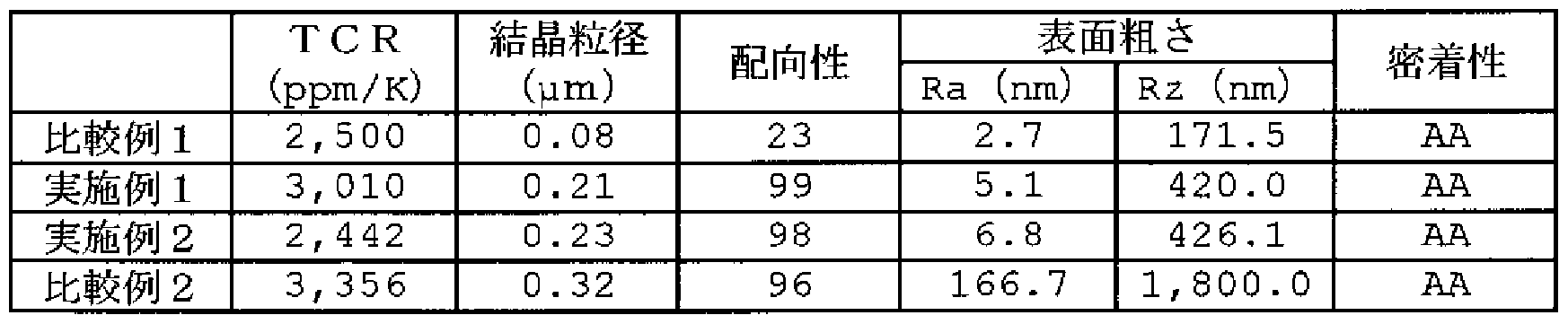
- the thin film sensor 2 thus obtained was measured for the temperature coefficient of resistance (TCR), crystal grain size, orientation, adhesion, and Ra and Rz described below. The results are shown in Table 1.
- a thin film sensor 3 was obtained in the same manner as in Example 1 except that the DC voltage was changed to 50 V in Example 1.
- the thin film sensor 3 was measured for the temperature coefficient of resistance (TCR), crystal grain size, orientation, adhesion, and Ra and Rz described below. The results are shown in Table 1.
- the thin film sensor 1 obtained in Comparative Example 1 was heat-treated at 1,000 ° C for 4 hours in an air atmosphere to obtain a thin film sensor 4.
- the thin film sensor 4 was measured for the temperature coefficient of resistance (TCR), crystal grain size, orientation, adhesion, and Ra and Rz described below. The results are shown in Table 1.
- the resistance temperature coefficient (TCR) was measured from the measurement of specific electrical resistance pT characteristics.
- the temperature coefficient of resistance refers to a value represented by the following (Equation 1).
- the longitudinal section of the thin film sensor manufactured as described above was polished and smoothed using a focused ion beam (FIB).
- This smoothed longitudinal section is equipped with an EBSD evaluation device (OIM Analysis, manufactured by TSL Solutions Co., Ltd.), a FE gun-type scanning electron microscope (JSM-6700F or Mioo SM-7000F, JEOL Ltd.)
- the image data of the crystal state pattern was obtained in accordance with the EBSD method using the EBSD analysis apparatus and the attached EBSD analyzer.
- the analysis menu “Gmin Size” of the EBSD analysis program (OIM Analysis, same as above) was selected, and crystal grains with a crystal rotation angle of 5 ° or more were observed to calculate the crystal grain diameter m). Note that the crystal grain size was calculated considering the intergranular defect as the triple grain boundary indicating the twin grain boundary.
- the longitudinal section of the thin film sensor manufactured as described above was smoothed using polishing and a focused ion beam (FIB).
- FE gun-type scanning electron microscope JSM-6700F or Miotsuo SM-700 OF, manufactured by JEOL Ltd.
- EBSD evaluation device OIM Analysis, manufactured by TSL Solutions, Inc.
- crystal pattern image data is selected from the analysis menu “Crystal Direction J” of the EBSD analysis program (OIM Analysis, same as above), and the “ND direction” of the laminated body or thin film sensor and the (111) plane orientation of the platinum crystal of the electrical resistor.
- the adhesion between the insulating substrate and the electric resistor was evaluated by the following wire pull test method.
- a gold wire (25 m ⁇ ) was bonded (bonded) on the gold electrode pad (18) of the thin film chip (thin film sensor). After that, the wire was pulled with a force of about 10g in the vertical direction of the thin film chip at room temperature.
- the evaluation criteria are as follows.
Abstract
[課題]熱処理などのコスト的に不利な工程を経ずに結晶を強配向化し、製品ごとの電気特性のばらつきが少ない薄膜センサの製造方法を提供すること。 [解決手段]絶縁基板と、該絶縁基板上に積層された金属からなる電気抵抗体とを有する薄膜センサの製造方法であって、 前記絶縁基板に、負の直流電圧を印加しながら、前記金属をスパッタリングして、前記電気抵抗体を形成する工程を有する ことを特徴とする薄膜センサの製造方法。
Description
明 細 書
薄膜センサの製造方法、薄膜センサおよび薄膜センサモジュール 技術分野
[0001] 本発明は、薄膜センサの製造方法、薄膜センサおよび薄膜センサモジュールに関 する。
背景技術
[0002] 従来から、各種物体又は流体の温度、流量、比熱、熱伝導性、濃度、液種、歪、応 力、湿度などを測定する温度センサ、流量センサ、比熱センサ、熱伝導性センサ、濃 度センサ、液種識別センサ、歪センサ、応力センサ、湿度センサなどの機能の発揮 のために用いられている薄膜センサモジュールとしては、熱量、流量、比熱、熱伝導 性、濃度、液種、歪、応力、湿度等の変化を電気信号に変換して温度を検出する電 気抵抗体を利用したものが広く使用されている。なかでも、感度の点で、抵抗温度係 数の絶対値が大きい白金族元素を利用した薄膜センサモジュールが広く用いられて V、るが、さらなる高感度化が求められて 、るのが現状である。
[0003] 一般に、抵抗体の抵抗温度係数は、抵抗体を構成する結晶の存在形態により、影 響を受けることが知られている (非特許文献 1)。例えば、特許文献 1及び非特許文献 2には、成膜後の積層体を熱処理するなどして、抵抗体を構成する結晶の粒径を大 型化することにより、高感度化を図る技術が開示されている。
[0004] 電気抵抗体を構成する結晶の粒径を大型化する方法としては、まず、基板上に白 金などの感温抵抗物質をメツキや蒸着等の積層技術によりパターンを形成させて堆 積させ、その後、数百〜千 °C程度で熱処理して結晶を成長させる方法などが挙げら れる。
[0005] し力しながら、感度を増大させることを目的として、過酷な熱処理条件により結晶を 成長させることは可能である力 この場合、多量の熱量を必要とする。また、これに付 随して、この熱量に耐え得る設備が必要となり、コスト的にも不利であった。また、熱 の負荷を考慮した材料や設計の選択が制限される。さらに、熱負荷により、表面粗さ が増大し、製品ごとのばらつきが大きくなり、生産安定性が低下するという問題が生じ
ていた。
[0006] また、特許文献 2には、白金薄膜抵抗体の製造の際に、白金薄膜と基板との密着 性を向上させるための層(たとえば)チタン層を両者の間に介在させることが記載され ている。
[0007] さらに、特許文献 1には、白金薄膜抵抗体の製造方法において、白金薄膜と基板と の間にチタン層を介在させることで基板に対する白金薄膜の密着性の向上を図りな 力 Sら、白金薄膜またはチタン層の形成のためのスパッタリングガス中に酸素を混入し ておくことで、高温ァニールによる白金薄膜の抵抗温度係数の十分な向上が可能と なることが記載されている。
[0008] しかしながら、白金薄膜と基板との密着性には、さらなる改善の余地があった。
特許文献 1:特開 2001— 291607号公報
特許文献 2:特開平 11― 354302号公報
非特許文献 1 :「薄膜'微粒子の構造と物性」、丸善、 139〜156頁(1974) 非特許文献 2 :「高 TCR白金薄膜の開発」、 IEEE Trans. SM.、 124卷、 7号、 24
2〜247頁(2004)
発明の開示
発明が解決しょうとする課題
[0009] 本発明は、上述の問題に鑑みてなされたものであって、熱処理などのコスト的に不 利な工程を経ずとも結晶を強配向化し、製品ごとの電気特性のばらつきが少ない薄 膜センサの製造方法を提供することを目的とする。
[0010] また本発明は、高感度であり、かつ電気抵抗体が剥がれ難い薄膜センサの製造方 法、ならびに該方法で製造される薄膜センサおよび該薄膜センサを有する薄膜セン サモジュールを提供することをさらなる目的としている。
課題を解決するための手段
[0011] 本発明の薄膜センサの製造方法は、
絶縁基板と、該絶縁基板上に積層された金属からなる電気抵抗体とを有する薄膜 センサの製造方法であって、
前記絶縁基板に、負の直流電圧を印加しながら、前記金属をスパッタリングして、
前記電気抵抗体を形成する工程を有する
ことを特徴としている。
[0012] 前記負の直流電圧の絶対値は、好ましくは 25V以上 150V以下である。
[0013] 前記薄膜センサの製造方法は、前記電気抵抗体を熱処理する工程を有さなくても よい。
[0014] 前記金属としては、ルテニウム、ロジウム、パラジウム、オスミウム、イリジウム及び白 金からなる群から選択された少なくとも 1つの金属を主成分とする金属が挙げられる。
[0015] 前記電気抵抗体を構成する金属の結晶粒径は 0. 2 μ m以上であり、前記電気抵 抗体の表面粗さ Raは lOnm以下であることが好ましい。
[0016] 前記薄膜センサは、前記絶縁基板上と前記電気抵抗体との間に、遷移金属を主成 分とする材料力もなる密着層をさらに有することが好ましい。
[0017] 前記薄膜センサは、前記絶縁基板上と前記密着層との間に、ケィ素と炭素、窒素、 フッ素および酸素力 なる群力 選ばれる元素との化合物力 なるケィ素化合物層を さらに有することが好ましい。
[0018] 前記薄膜センサとしては、温度センサ、流量センサ、比熱センサ、熱伝導性センサ
、濃度センサ、液種識別センサ、歪センサ、応力センサ、湿度センサ力 なる群から 選択されたセンサが挙げられる。
[0019] 本発明の薄膜センサは、前記薄膜センサの製造方法で製造された薄膜センサであ ることを特徴とする。
[0020] 本発明の薄膜センサモジュールは、前記薄膜センサを有することを特徴としている 発明の効果
[0021] 本発明によれば、電気特性を保持しつつ、コスト的にも有利で、製品ごとの電気特 性のばらつきが少ない薄膜センサが得られる。
[0022] また本発明の一態様によれば、高感度であり、電気抵抗体が剥がれ難!ヽ薄膜セン サの製造方法、ならびに該方法で製造される薄膜センサおよび該薄膜センサを有す る薄膜センサモジュールが提供される。
図面の簡単な説明
[0023] [図 1]薄膜センサ (薄膜チップ)の一態様の概略図である。
[図 2]薄膜センサ (薄膜チップ)の一態様の概略図である。
[図 3]本発明の薄膜センサモジュール例示した概略図である。
[図 4]本発明の薄膜センサモジュールを例示した概略断面図であって、(a)は、平面 縦断面図であり、(b)は、側方縦断面図である。
符号の説明
[0024] 10 薄膜センサ (薄膜チップ)
11 絶縁基板
12 ケィ素化合物層
13 密着層
14 電 几.体
16 保護膜
18 ボンディングノ ッド
20 薄膜センサモジュール
22 ハウジング
24 フィンプレート
26 出力端子
32 ボンディングワイヤ
34 第 1大径部
36 第 2大径部
38 切欠部
発明を実施するための最良の形態
[0025] <薄膜センサ >
図 1は、本発明の薄膜センサ (薄膜チップ)の概略図である。薄膜センサ 10は、電 気的に絶縁性を有する絶縁基板 11と、電気抵抗体 14とを少なくとも有する。
[0026] 薄膜センサ 10は、図 2に示すように、絶縁基板 11と電気抵抗体 14との密着性を向 上させることを目的として、絶縁基板 11と電気抵抗体 14との間に密着層 13を有して もよぐさらに絶縁基板 11と密着層 13との間にケィ素化合物層 12を有してもよい。薄
膜センサ 10は、薄膜センサの物理的な損傷の防止を目的として、薄膜センサ 10の 表面に保護膜 16を有してもよい。薄膜センサ 10は、薄膜センサ 10と外部の部材とを 電気的に接続するボンディングパッド 18を有してもよい。
[0027] なお、本発明においては、絶縁基板力も電気抵抗体に向力 方向を、便宜上「上」 と称することがある。
[0028] 絶縁基板 11の材料としては、絶縁性を有する材料であれば、特に制約はなぐ例 えば、シリコン、アルミナ等が挙げられる。絶縁基板 11の形状は、種々の形状とする ことができ、例えば、図 1に示すように矩形であってもよぐ楕円形、円形であってもよ い。また、絶縁基板 11の膜厚は、 300〜1, 000 /z m程度であってもよい。
[0029] 電気抵抗体 14は、温度、流量等の本発明における薄膜センサの測定対象となる指 標の変化に反応して、抵抗値が変化する材料で製造されたものであれば、特に制約 はなぐ電気抵抗体 14の材料としては、例えば、白金族、鉄、ニッケルコバルト、銅な どの遷移金属が挙げられる。薄膜センサを温度センサとして用いる場合であれば、電 気抵抗体 14の材料は、白金族元素 (ルテニウム、ロジウム、パラジウム、オスミウム、ィ リジゥム、白金)のうち少なくとも一種類以上の元素を主成分とする金属又はこれら金 属の合金が用いられる。特に、製膜の容易さ、特性の安定性、コストの面から、白金 力 り好ましい。電気抵抗体 14は、このような材料を用いて、所望の膜厚や、所望の パターンに成形されればよぐ例えば、膜厚は 0. 1〜1 μ m程度であってもよい。
[0030] 密着層 13の材料は、絶縁基板 11の温度—抵抗特性に影響を与えな 、材料及び 範囲において種々選択すればよぐその例として、遷移金属を主成分とする材料が 挙げられ、この材料の中には、金属として、遷移金属以外の金属が含まれていてもよ い。この遷移金属を主成分とする材料としては、具体的にはチタン (Ti)、クロム (Cr) 、 TiO、 TiBaOなどが挙げられ、中でも密着性の観点力 チタンおよびクロムが好ま
2
しい。遷移金属を主成分とする材料の中には、遷移金属が通常 10〜: L00重量%、 好ましくは 60〜: L00重量%含まれる。密着層の厚みは、例えば、 0. 002-0. l ^ m であることが好ましぐ 0. 005〜0. 05 mであることがより好ましい。
[0031] ケィ素化合物層 12は、ケィ素と、炭素、窒素、フッ素および酸素からなる群力も選 ばれる元素との化合物力もなる。このような化合物としては、 SiO、 SiN、 SiON、 SiC
、 SiOC、 SiOFなどが挙げられ、中でも成膜の容易さの観点力 SiOが好ましい。
2
[0032] ケィ素化合物層 12の厚さは、好ましくは 50〜5, 000nm、さらに好ましくは 100〜1 , OOOnmである。
[0033] 電気抵抗体 14は、密着層 13と、さらにこのケィ素化合物層 12とを介して絶縁基板 11に積層されると、絶縁基板 11に強固に密着し、剥がれ難い。
[0034] 保護膜 16の材料としては、上述の目的を達成し得る材料であれば特に制約はなく 、例えば、榭脂ゃガラス等が挙げられる。また、保護膜 16の膜厚は、約 1 μ m程度で あってもよい。
[0035] ボンディングパッド 18の材料としては、良好な導電性を有するものであれば特に制 約はなぐ例えば、金 (Au)、白金などが挙げられる。また、ボンディングパッド 18は、 適用される形態に応じて種々の形状であってもよぐ例えば、縦横 0. 2 X 0. 15mm, 厚み 0. 1 m程度の形状であってもよい。
[0036] なお、本発明の薄膜センサは、電気抵抗体の抵抗値に影響を与える指標を測定す る装置に用いることが可能であって、その例としては、温度センサ、流量センサ、比熱 センサ、熱伝導性センサ、濃度センサ、液種識別センサ、歪センサ、応力センサ、湿 度センサ等が挙げられる。
[0037] <本発明における電気抵抗体の結晶の存在形態 >
本発明の薄膜センサにおいて、電気抵抗体を構成する結晶は、特定の配向を有す る形態で存在する。本発明では、この配向の状態を、下述する「配向性」で規定する 。本発明において、「配向性」とは、電気抵抗体の層の面垂直方向(ND方向)から 1 0° 以内に配向している結晶(すなわち、電気抵抗体を構成する結晶)の(111)面の 割合をいう。本発明の薄膜センサにおいては、この割合が 90%以上であることが好ま しい。なお、この「配向性」の値は、後述する実施例の欄に記載の方法により求められ る値である。
[0038] 一般的に、電気抵抗体の結晶状態は、電気抵抗体における温度上昇に伴う抵抗 値の変化に影響を及ぼすことが知られている。結晶状態、特に結晶の粒径が大型化 することにより、抵抗温度係数の勾配が上昇することが知られ、粒径の大型化は、薄 膜センサの感度を上昇させる手法の一つとして汎用されている。
[0039] 一方、本発明にお ヽては、電気抵抗体を構成する結晶の存在形態に着目した。つ まり、本発明者らは、結晶の存在形態、特に結晶の配向性を制御することで、電気抵 抗体の抵抗温度係数が向上することを見出した。本発明のように配向性を制御する ことにより抵抗温度係数が向上する機構は定かではないが、結晶方位が特定の方向 に揃うことにより、結晶の電気的特性が向上されることが考えられる。
[0040] また、電気抵抗体を構成する結晶は、繊維状配向組織を有し、該繊維状配向組織 において、該結晶の(111)面が該電気抵抗体の層の面垂直方向を回転軸としてい ることが好ましい。このような組織を有することにより、より一層電気的特性が向上され る。なお、この繊維状配向組織の観察には、組織観察に用いる種々の手法を用いて 観察すればよぐ例えば、下述の EBSD評価装置を用いて観察してもよい。
[0041] なお、本発明にお 、て、結晶の配向性の評価は、 EBSD (後方散乱電子回折バタ ーン; Electron Backscatter Diffraction Pattern)法を用いて行った。無機材 料の結晶配構成の評価としては、 X線回折装置 (XRD)が一般的に用いられている 力 この装置では、結晶構造全体の平均的な情報しか得ることが出来ず、結晶構造 を構成する個々の結晶粒の存在形態を評価することは出来ない。一方、個々の結晶 粒の配向を評価するには、従来、透過型電子顕微鏡 (TEM)が一般的に用いられて いるが、結晶構造に含まれる結晶粒について統計的な評価を行うのは、現実的に不 可能である。
[0042] 一方、 EBSD評価装置を用いれば、個々の結晶粒の存在形態に係る評価を迅速 に行うことができ、結晶粒径や粒度分布、結晶の配向性や歪計算などの評価が可能 である。
[0043] 本発明の薄膜センサにおいて、電気抵抗体の表面粗さ (Ra)は、好ましくは 10nm 以下、さらに好ましくは 5nm以下であり、その下限値は、特に制限はされないが、通 常 lnm程度である。また、表面粗さ (Rz)は、好ましくは 1. 以下、さらに好ましく は 0. 5 m以下であり、その下限値は、特に制限はされないが、通常 0. 程度 である。これらの範囲力 外れると、パターン成型の際に、一定した電気特性が得ら れず、生産性が低下してしまうことにもなる。
[0044] また、電気抵抗体を構成する結晶の粒径は、好ましくは 0. 2 μ m以上、さらに好ま
しくは 0. 以上であり、その上限値は、特に制限されないが、通常 5. O /z m程度 である。なお、この「結晶粒径」の値は、後述する実施例の欄に記載の方法により求 められる値である。
[0045] 本発明の薄膜センサの抵抗温度係数は、好ましくは 3, OOOppmZK以上、さらに 好ましくは 3, 300ppm/K以上であり、その上限値は 3, 900ppm/K程度である。
[0046] <薄膜センサの製造方法 >
本発明の薄膜センサの製造方法においては、絶縁基板上にスパッタリング法により 、電気抵抗体を積層する。
[0047] このスパッタリングは、絶縁基板に、負の直流のノィァス電圧を印加しながら行う。こ の電圧の絶対値は、好ましくは 25V以上 150V以下、さらに好ましくは 50Vよりも大き く 150V未満、特に好ましくは 75V以上 125V以下である。この範囲を外れると、製造 される薄膜センサの成膜性や TCRなどの電気特性が実用的でなくなる。
[0048] この負の直流のバイアス電圧を変化させることにより電気抵抗体の TCRを変化させ ることができるが、この理由としては、必ずしも定かではないが、たとえば以下のような 理由が考えられる。
(1)すなわち、バイアス電圧を大きくするとスパッタ粒子のエネルギーが高められるた め、基板に到達した粒子がエネルギー的に安定なサイトまで移動でき、その結果、緻 密で結晶粒径が大きぐかつ配向性の高い膜 (電気抵抗体)が形成される。
(2) (1)の結果として、不純物(特に密着層の成分である Tiなど)の拡散が抑制され、 電気抵抗体の TCRが高められる。
[0049] スパッタリングを行う際の真空度、圧力等の条件には、特に制限はない。
[0050] スパッタリングの際、導入ガスのアルゴンなどの不活性ガスには、酸素ガスを混合し てもよい。不活性ガスへの酸素の混合量は、例えば標準状態で 0. 5〜30体積%の 範囲内とすることができ、好ましくは 2〜20体積%の範囲内である。 0. 5体積%未満 であると、密着層を構成する金属原子の一部が電気抵抗体の内部に拡散し、その抵 抗温度係数 (TCR)を低下させる。 30体積%以上であると、電気抵抗体を構成する 結晶の内部に酸素が固溶するため、その抵抗温度係数 (TCR)が低下する。
[0051] 電気抵抗体として白金薄膜を形成する場合であれば、たとえば、以下のような条件
で蒸着を行うことができる。
[0052] 装置: RFスパッタリング装置
電極間距離: 20〜60mm
到達真空度: 3. 0 X 10_4Pa以下
成膜圧力: 4〜12Pa
成膜電力: 180〜250W
成膜温度:室温〜 80°C。
[0053] さらに、電気抵抗体を構成する結晶の内部に酸素が固溶したり、不純物として取り 込まれ、電気抵抗体の抵抗温度係数 (TCR)が低下することを防止するために、スパ ッタリングの際には、大気、酸素又は水分等に触れることなく電気抵抗体を連続成膜 することが好ましい。
[0054] 本発明の積層体および該積層体力ゝらなる薄膜センサに密着層を設ける場合には、 電気抵抗体の積層の前に、絶縁基板上にスパッタリングなどの積層技術を用 、て密 着層を積層し、その後、電気抵抗体を上述の通りに積層すればよい。密着層の積層 後は、大気、酸素又は水分等に触れることなくその後の工程を行うことが好ましい。密 着層の積層条件としては、特に制約はなぐ後に行う電気抵抗体の積層条件に合わ せて、適宜選択すればよい。密着層としてチタン (Ti)層を形成する場合であれば、 たとえば、以下のような条件で蒸着を行うことができる。
[0055] 蒸着手段:スパッタリング法
装置:マグネトロンスパッタリング装置
到達真空度: 6. 0 X 10— 5Pa以下
成膜圧力: 0. l〜2Pa
ガス流量: 10〜180SCCM
成膜電力: 400〜1, 400W
成膜温度:室温〜 250°C。
[0056] 薄膜センサにケィ素化合物層を設ける場合には、密着層の積層の前に、絶縁基板 の一表面にケィ素化合物層を積層する。
[0057] ケィ素化合物層は、ゾルゲル法、スピンコート法、 CVD法、スパッタリング法、など
の手段により形成することができ、具体的には、たとえば以下のような条件で製造す ることがでさる。
[0058] 積層手段:スピンコート法
装置:スピンコーター
原料:塗布型 SiO系被膜形成材料 (SOG)
2
回転数: 1, 000〜6, OOOrpm
温度: 450〜1, 000。C。
[0059] 次に、得られた積層体 (すなわち、絶縁基板および電気抵抗体、ならびに任意の密 着層、および任意のケィ素化合物層を含む積層体)に対して、例えば 900°C〜1100 °Cの範囲内でアニーリングを行うことで、薄膜センサが得られる。
[0060] ァニール温度が 900°C未満であると、薄膜センサの抵抗温度係数が低下する傾向 にある。また、 1100°Cを越えると、薄膜センサの表面状態が劣化する傾向にある。ァ ニール時間は、例えば 4時間以上 8時間未満とすることができる。とすることができる。 ァニール時間が 4時間未満、すなわち短過ぎる場合には、電気抵抗体の抵抗値の経 時変化率が大きくなる傾向にある。一方、ァニール時間が 8時間よりも長くなると、白 金の結晶粒が粗大化しすぎ、表面粗さが増大し、基板材料内での均一性が低下す る傾向がある。
[0061] 電気抵抗体は、エッチング等の手段により、種々のパターンに成形されてもよい。
例えば、エッチング法などにより、電気抵抗体を、幅が例えば 5〜25 /ζ πιで、全長が 例えば 4〜23cmの蛇行パターン形状に加工してもよい。
[0062] <薄膜センサモジユーノレ >
次に、本発明の薄膜センサモジュールについて、説明する。本発明の薄膜センサ モジュールは、測定対象となる物体や流体と熱的に接続される部材と、この部材と熱 的に接続された上述の薄膜センサと、この薄膜センサと電気的に接続された部材とを 有する。この構成を図 3及び図 4に例示する。
[0063] 図 3は、本発明の薄膜センサモジュール (たとえば、温度センサモジュール)を例示 した概略図であり、図 4は、本発明の薄膜センサモジュール (たとえば、温度センサモ ジュール)を例示した概略断面図であって、(a)は、平面縦断面図であり、(b)は、側
方縦断面図である。本発明の薄膜センサモジュール (たとえば、温度センサモジユー ル) 20は、ハウジング 22の内部に、フィンプレート 24と出力端子 26とが固着された薄 膜センサ(たとえば、温度センサ) 10を有する。
[0064] ハウジング 22の材料としては、熱伝導性の低!、材料であれば種々の材料を使用し 得る。また、測定対象である物体や流体等に応じて、耐薬品性ゃ耐油性を付与され た材料も使用し得る。これらの特性を有する例としては、例えば、エポキシ榭脂ゃポリ ブチレンテレフタレート(PBT)、ポリフエ-レンスルフイド(PPS)等が挙げられる。また 、薄膜センサモジュールの形状は、薄膜センサモジュールを適用する態様に応じて、 種々の形態とすればよい。例えば、ハウジング 22は、図 3及び図 4 (B)のように、出力 端子 26が突出する第 1大径部 34と、第 1大径部 34と間隔を置いて下方に位置する 第 2大径部 36とを有し、第 1大径部 34と第 2大径部 36との間には、断熱用の空隙を 形成するための切欠部 38を有していてもよい。なお、ハウジング 22は、この形態に限 定されるものではない。
[0065] フィンプレート 24は、熱伝導性の良好な材料力もなれば特に制約はなぐ例えば、 銅、アルミニウム、タングステン、ジュラルミン、銅—タングステン合金等力もなる。また 、フィンプレート 24は、薄膜センサモジュールの適用に応じて、適宜種々の形状とす ればよぐ例えば、厚さ 200 /z m程度の薄板であってもよい。なお、フィンプレート 24 と薄膜センサ 10との固着用の材料としては、熱導電性を有する材料であればいかな る材料をも用いることができ、例えば、銀ペーストが挙げられる。
[0066] 出力端子 26は、導電性を有する材料力もなるものであれば特に制約はなぐこの材 料としては、銅、アルミニウム等が挙げられる。出力端子 26は、ボンディングワイヤ 32 を介して薄膜センサ 10と電気的に接続される。出力端子 26の形状は、図 3では、榭 脂ハウジング 2の外部に、直線状に一列に並置されて突出し、かつ、前記直線状の 列の一端力も他端に向力つて、榭脂ハウジング 2からの突出長さが漸増 (漸減)して いるように示されるが、適用される形態に応じて種々の形状に成形されたものであれ ばよい。なお、図 3の形状を有することにより、薄膜センサモジュール 20を上力も押え るセンサ押圧板や、出力端子 26と接続されて回路を形成する流量検出回路基板の 装着を、容易に行なうことができる。また、これらセンサ押圧板や流量検出回路基板
の装着の際に薄膜センサモジュール 20を痛めるおそれも小さくなる。
[0067] [実施例]
以下、本発明について実施例に基づいてさらに具体的に説明するが、本発明は、 係る実施例により何ら限定されるものではない。
[0068] (比較例 1)
アルミナ基板(寸法:直径 100mmの円盤、厚み: 385 m)上に、以下の条件でス ピンコート法により膜厚 300nmの SiO層を形成した。
2
[0069] 装置:スピンコーター
原料:塗布型 SiO系被膜形成材料
2
(東京応化工業 (株)製、原料: OCD (商品名)、シロキサン系材料) 回転数: 1, 000rpmX 5s→5, 000rpm X 30s
温度: 695°C。
[0070] 次に、このようにして形成された SiO層上に、金属チタン (純度 99. 99%)をターゲ
2
ットとして、以下の条件でスパッタリングを行い、膜厚 30nmのチタン層を形成させた。
[0071] 装置:マグネトロンスパッタリング装置
到達真空度: 6. 0 X 10_5Pa未満
成膜圧力: 0. 86Pa
ガス流量: 180SCCM [Ar: 0 = 10 : 0 (標準状態での体積比) ]
2
成膜電力: 1, OOOW(DC)
成膜温度: 250°C。
[0072] 次に、このようにして形成されたチタン層上に、白金 (純度 99. 9%)をターゲットとし て、以下の条件でスパッタリングを行い、膜厚 400nmの電気抵抗体を形成させた。
[0073] 装置:マグネトロンスパッタリング装置
到達真空度: 6. 0 X 10_5Pa未満
成膜圧力: 0. 18Pa
ガス流量: 10SCCM [Ar: 0 = 9 : 1 (標準状態での体積比) ]
2
成膜電力: 500W(RF)
成膜温度: 250°C。
[0074] このようにして得られた薄膜センサ 1につ 、て、下述の抵抗温度係数 (TCR)、結晶 粒径、配向性、密着性ならびに Raおよび Rzの測定を行った。結果を表 1に示す。
[0075] (実施例 1)
比較例 1と同様の操作によりアルミナ基板上に SiO層およびチタン層を形成した後
2
、該チタン層上に、白金 (純度 99. 9%)をターゲットとして、以下の条件でスパッタリ ングを行い、膜厚 400nmの電気抵抗体を形成することにより、薄膜センサ 2を製造し た。
[0076] 装置: RFスパッタリング装置
電極間距離: 35mm
ターゲット直径: 7. 5mm
到達真空度: 3. 0 X 10_5Pa未満
成膜圧力: 9Pa
基板に印加する直流電圧: 100V
成膜電力: 220W(RF)
成膜温度: 80°C。
[0077] このようにして得られた薄膜センサ 2につ 、て、下述の抵抗温度係数 (TCR)、結晶 粒径、配向性、密着性ならびに Raおよび Rzの測定を行った。結果を表 1に示す。
[0078] (実施例 2)
実施例 1において、直流電圧を 50Vに変更した以外は、実施例 1と同様に処理し 、薄膜センサ 3を得た。この薄膜センサ 3について、下述の抵抗温度係数 (TCR)、結 晶粒径、配向性、密着性ならびに Raおよび Rzの測定を行った。結果を表 1に示す。
[0079] (比較例 2)
比較例 1で得た薄膜センサ 1を、大気雰囲気下、 1, 000°Cで 4時間の熱処理し、薄 膜センサ 4を得た。この薄膜センサ 4について、下述の抵抗温度係数 (TCR)、結晶 粒径、配向性、密着性ならびに Raおよび Rzの測定を行った。結果を表 1に示す。
[0080] <抵抗温度係数 (TCR)の測定 >
対象となる薄膜センサについて、比電気抵抗 p—T特性の測定から、抵抗温度係 数 (TCR)を測定した。
[0081] なお、本発明において、抵抗温度係数とは、以下の(式 1)で示される値をいう。
[0082] (式1) : « = (1 !¾ >< ((11^7(1丁) 106
a:抵抗温度係数 (ppmZ°C)
T:任意の絶対温度 (K)
R: T (K)におけるゼロ負荷抵抗値( Ω )。
[0083] <結晶粒径 >
上述のように製造された薄膜センサの縦断面を研磨及び集束イオンビーム (FIB) を用いて平滑にした。この平滑にされた縦断面について、 EBSD評価装置(OIM A nalysis,株式会社 TSLソリューションズ社製)を搭載した FE銃型の走査型電子顕微 鏡 (JSM— 6700F又〖お SM— 7000F、日本電子株式会社製)および付属の EBSD 解析装置を用いて、 EBSD法に準じて、結晶状態のパターンの画像データを得た。 この画像データについて、 EBSD解析プログラム(OIM Analysis,同上)の分析メ ニュー「Gmin Size」を選択し、結晶回転角が 5° 以上の結晶粒を観察し、結晶粒 径 m)を算出した。なお、結晶粒径にっ 、ては、双晶粒界を示す∑ 3粒界を粒内 欠陥と考慮して算出した。
[0084] <配向性 >
上述のように製造された薄膜センサの縦断面を、研磨及び集束イオンビーム (FIB) を用いて平滑にした。 EBSD評価装置(OIM Analysis,株式会社 TSLソリューショ ンズ社製)を搭載した FE銃型の走査型電子顕微鏡 (JSM— 6700F又〖お SM— 700 OF、日本電子株式会社製)および付属の EBSD解析装置を用いて、この平滑にされ た縦断面について、 EBSD法に準じて、結晶状態のパターンの画像データを得た。 この画像データを、 EBSD解析プログラム(OIM Analysis,同上)の分析メニュー「 Crystal DirectionJを選択し、積層体又は薄膜センサの「ND方向」と、電気抵抗 体の白金結晶の(111)面方位とのずれが 10度以内にある結晶粒の全結晶粒に対 する割合を算出する条件で解析し、この割合を、「配向性」とした。なお、粒回転角が 5° 以上にあるものを結晶粒界とし、 5° 以内である集合体をひとつの結晶粒として 疋'した。
[0085] <表面粗さ Ra及び Rzの測定 >
表面粗さ Ra及び Rzは、上述の各薄膜センサを、光干渉式三次元構造解析顕微鏡 (New View5032、 Zygo社製)にて測定した。測定には、白色光を用いて 100倍ミ ラウレンズを使用し、 54 X 72 /z mの範囲を測定した。このようにして得た三次元測定 面から、表面粗さ Ra及び Rzを得た。
[0086] <密着性>
上述のように製造された薄膜センサのそれぞれにつ 、て、以下のワイヤープルテス ト方法により、絶縁基板と電気抵抗体との密着性を評価した。
*ワイヤープルテスト方法
薄膜チップ (薄膜センサ)の金電極パッド( 18)上に、金線 (25 m φ )を接合 (ボン デイング)させた。その後、室温にて、薄膜チップの垂直方向に 10g重程度の力で金 線を引っ張った。評価基準は以下のとおりである。
[0087] AA- · '金電極パッドおよび電気抵抗体は金線から剥離せず、金線が破断した。
[0088] CC · · ·金電極パッドおよび電気抵抗体は金線から剥離した。
[0089] [表 1]
【表 1】
[0090] 以上、本発明の好適な実施の形態により本発明を説明した。ここでは特定の具体 例を示して本発明を説明したが、特許請求の範囲に定義された本発明の広範な趣 旨および範囲力 逸脱することなぐこれら具体例に様々な修正および変更を加える ことができることは明らかである。すなわち、具体例の詳細および添付の図面により本 発明が限定されるものと解釈してはならない。
Claims
[1] 絶縁基板と、該絶縁基板上に積層された金属からなる電気抵抗体とを有する薄膜 センサの製造方法であって、
前記絶縁基板に、負の直流電圧を印加しながら、前記金属をスパッタリングして、 前記電気抵抗体を形成する工程を有する
ことを特徴とする薄膜センサの製造方法。
[2] 前記負の直流電圧の絶対値が 25V以上 150V以下であることを特徴とする請求項
1に記載の薄膜センサの製造方法。
[3] 前記電気抵抗体を熱処理する工程を有さな!/ヽことを特徴とする請求項 1または 2〖こ 記載の薄膜センサの製造方法。
[4] 前記金属が、ルテニウム、ロジウム、パラジウム、オスミウム、イリジウム及び白金から なる群から選択された少なくとも 1つの金属を主成分とする金属であることを特徴とす る請求項 1〜3のいずれかに記載の薄膜センサの製造方法。
[5] 前記電気抵抗体を構成する金属の結晶粒径が 0. 2 μ m以上であり、前記電気抵 抗体の表面粗さ Raが lOnm以下であることを特徴とする請求項 1〜4のいずれかに 記載の薄膜センサの製造方法。
[6] 前記薄膜センサが、前記絶縁基板上と前記電気抵抗体との間に、遷移金属を主成 分とする材料からなる密着層をさらに有することを特徴とする請求項 1〜5のいずれか に記載の薄膜センサの製造方法。
[7] 前記薄膜センサが、前記絶縁基板上と前記密着層との間に、ケィ素と炭素、窒素、 フッ素および酸素力 なる群力 選ばれる元素との化合物力 なるケィ素化合物層を さらに有することを特徴とする請求項 6に記載の薄膜センサの製造方法。
[8] 前記薄膜センサが、温度センサ、流量センサ、比熱センサ、熱伝導性センサ、濃度 センサ、液種識別センサ、歪センサ、応力センサ、湿度センサ力 なる群力 選択さ れたセンサであることを特徴とする請求項 1〜7のいずれかに記載の薄膜センサの製 造方法。
[9] 請求項 1〜8のいずれかに記載の製造方法で製造された薄膜センサ。
[10] 請求項 9に記載の薄膜センサを有することを特徴とする薄膜センサモジュール。
Priority Applications (2)
| Application Number | Priority Date | Filing Date | Title |
|---|---|---|---|
| US12/294,849 US20100245030A1 (en) | 2006-03-28 | 2007-03-28 | Processes for Producing Thin-Film Sensors, Thin-Film Sensors and Thin-Film Sensor Modules |
| EP07740027A EP2009647A1 (en) | 2006-03-28 | 2007-03-28 | Method for fabricating thin film sensor, thin film sensor and thin film sensor module |
Applications Claiming Priority (2)
| Application Number | Priority Date | Filing Date | Title |
|---|---|---|---|
| JP2006088415 | 2006-03-28 | ||
| JP2006-088415 | 2006-03-28 |
Publications (1)
| Publication Number | Publication Date |
|---|---|
| WO2007114143A1 true WO2007114143A1 (ja) | 2007-10-11 |
Family
ID=38563412
Family Applications (1)
| Application Number | Title | Priority Date | Filing Date |
|---|---|---|---|
| PCT/JP2007/056589 WO2007114143A1 (ja) | 2006-03-28 | 2007-03-28 | 薄膜センサの製造方法、薄膜センサおよび薄膜センサモジュール |
Country Status (3)
| Country | Link |
|---|---|
| US (1) | US20100245030A1 (ja) |
| EP (1) | EP2009647A1 (ja) |
| WO (1) | WO2007114143A1 (ja) |
Cited By (2)
| Publication number | Priority date | Publication date | Assignee | Title |
|---|---|---|---|---|
| JP2011104690A (ja) * | 2009-11-16 | 2011-06-02 | Mitsubishi Materials Corp | 硬質被覆層がすぐれた耐チッピング性を発揮する表面被覆切削工具 |
| JPWO2012086529A1 (ja) * | 2010-12-22 | 2014-05-22 | 株式会社マーレ フィルターシステムズ | キャニスタの検出装置 |
Families Citing this family (7)
| Publication number | Priority date | Publication date | Assignee | Title |
|---|---|---|---|---|
| US8465812B2 (en) * | 2009-03-23 | 2013-06-18 | The Boeing Company | Durable transparent intelligent coatings for polymeric transparencies |
| US9963777B2 (en) * | 2012-10-08 | 2018-05-08 | Analog Devices, Inc. | Methods of forming a thin film resistor |
| EP2914957A4 (en) * | 2012-10-30 | 2016-06-15 | Edwards Lifesciences Corp | ANALYTE SENSOR AND METHODS OF MANUFACTURE |
| CA2867075C (en) * | 2013-02-22 | 2016-09-20 | Yong Il Cho | Heater module for heater of fluid infusion apparatus and manufacturing method thereof |
| US9982900B2 (en) | 2014-01-29 | 2018-05-29 | Trane International Inc. | Method of attaching electrodes to plated thermoset plastic heated blower housing |
| US9972425B2 (en) * | 2015-06-30 | 2018-05-15 | Qorvo Us, Inc. | Frequency-dependent resistor and circuitry employing the same |
| WO2019219586A1 (en) * | 2018-05-16 | 2019-11-21 | Ab Sandvik Materials Technology | Metallic tube structure with a sensor arrangement |
Citations (6)
| Publication number | Priority date | Publication date | Assignee | Title |
|---|---|---|---|---|
| JPH01176316A (ja) * | 1987-12-29 | 1989-07-12 | Nec Corp | 磁気記録媒体およびその製造方法 |
| JPH02226017A (ja) * | 1988-12-23 | 1990-09-07 | Honeywell Inc | 薄膜白金素子用接着層を有するセンサ構造 |
| JPH11354302A (ja) | 1998-06-09 | 1999-12-24 | Mitsui Mining & Smelting Co Ltd | 薄膜抵抗素子 |
| JP2001012982A (ja) * | 1999-06-29 | 2001-01-19 | Mitsui Mining & Smelting Co Ltd | 流量センサー及び温度センサー |
| JP2001091321A (ja) * | 1999-09-21 | 2001-04-06 | Mitsui Mining & Smelting Co Ltd | 流量センサーユニット及びこれを用いた流量計 |
| JP2001291607A (ja) | 2000-04-04 | 2001-10-19 | Mitsui Mining & Smelting Co Ltd | 白金薄膜抵抗体の製造方法 |
Family Cites Families (6)
| Publication number | Priority date | Publication date | Assignee | Title |
|---|---|---|---|---|
| US4533605A (en) * | 1980-09-09 | 1985-08-06 | Westinghouse Electric Corp. | Article such as jewelry or a wristwatch component having composite multi-film protective coating |
| US4624137A (en) * | 1981-10-09 | 1986-11-25 | Honeywell Inc. | Semiconductor device |
| JPS5922399B2 (ja) * | 1981-10-14 | 1984-05-26 | 日本電気株式会社 | 多層セラミツク基板 |
| JPS61188901A (ja) * | 1985-02-16 | 1986-08-22 | 株式会社日本自動車部品総合研究所 | 流量センサ用膜式抵抗 |
| EP1193477A4 (en) * | 1999-06-24 | 2006-10-18 | Mitsui Mining & Smelting Co | FLOW DETECTOR, FLOWMETER AND FLOW SENSOR |
| JP5138134B2 (ja) * | 2001-07-16 | 2013-02-06 | 株式会社デンソー | 薄膜式センサの製造方法ならびにフローセンサの製造方法 |
-
2007
- 2007-03-28 US US12/294,849 patent/US20100245030A1/en not_active Abandoned
- 2007-03-28 EP EP07740027A patent/EP2009647A1/en not_active Withdrawn
- 2007-03-28 WO PCT/JP2007/056589 patent/WO2007114143A1/ja active Application Filing
Patent Citations (6)
| Publication number | Priority date | Publication date | Assignee | Title |
|---|---|---|---|---|
| JPH01176316A (ja) * | 1987-12-29 | 1989-07-12 | Nec Corp | 磁気記録媒体およびその製造方法 |
| JPH02226017A (ja) * | 1988-12-23 | 1990-09-07 | Honeywell Inc | 薄膜白金素子用接着層を有するセンサ構造 |
| JPH11354302A (ja) | 1998-06-09 | 1999-12-24 | Mitsui Mining & Smelting Co Ltd | 薄膜抵抗素子 |
| JP2001012982A (ja) * | 1999-06-29 | 2001-01-19 | Mitsui Mining & Smelting Co Ltd | 流量センサー及び温度センサー |
| JP2001091321A (ja) * | 1999-09-21 | 2001-04-06 | Mitsui Mining & Smelting Co Ltd | 流量センサーユニット及びこれを用いた流量計 |
| JP2001291607A (ja) | 2000-04-04 | 2001-10-19 | Mitsui Mining & Smelting Co Ltd | 白金薄膜抵抗体の製造方法 |
Non-Patent Citations (3)
| Title |
|---|
| "HAKUMAKU, BIRYUUSHI NO KOUZOU TO BUSSEI", 1974, MARUZEN, pages: 139 - 156 |
| "KOU TCR HAKKIN HAKUMAKU NO KAIHATSU", IEEE TRANS. SM., vol. 124, no. 7, 2004, pages 242 - 247 |
| SHI J. ET AL.: "The interaction between platinum films and silicon substrates: Effects of substrate bias during sputtering deposition", JOURNAL OF APPLIED PHYSICS, vol. 88, no. 3, 2000, pages 1679 - 1683, XP001065089 * |
Cited By (2)
| Publication number | Priority date | Publication date | Assignee | Title |
|---|---|---|---|---|
| JP2011104690A (ja) * | 2009-11-16 | 2011-06-02 | Mitsubishi Materials Corp | 硬質被覆層がすぐれた耐チッピング性を発揮する表面被覆切削工具 |
| JPWO2012086529A1 (ja) * | 2010-12-22 | 2014-05-22 | 株式会社マーレ フィルターシステムズ | キャニスタの検出装置 |
Also Published As
| Publication number | Publication date |
|---|---|
| EP2009647A1 (en) | 2008-12-31 |
| US20100245030A1 (en) | 2010-09-30 |
Similar Documents
| Publication | Publication Date | Title |
|---|---|---|
| WO2007114143A1 (ja) | 薄膜センサの製造方法、薄膜センサおよび薄膜センサモジュール | |
| WO2007091686A1 (ja) | 積層体、薄膜センサ、薄膜センサモジュールおよび薄膜センサの製造方法 | |
| JP2023154057A (ja) | ひずみゲージ、センサモジュール | |
| EP3690385B1 (en) | Strain gauge and sensor module | |
| TWI382428B (zh) | Touch panel sensor | |
| WO2013147282A1 (ja) | 温度センサ及びその製造方法 | |
| US11326966B2 (en) | Strain gauge with improved design to reduce pinholes and damage | |
| CN102826602B (zh) | 热敏电阻材料、温度传感器及其制造方法 | |
| US20110068890A1 (en) | Ntc thin film thermal resistor and a method of producing it | |
| CN103688320A (zh) | 薄膜热敏电阻元件及其制造方法 | |
| WO2013147290A1 (ja) | サーミスタ用金属窒化物膜及びその製造方法並びにフィルム型サーミスタセンサ | |
| JP2023129465A (ja) | ひずみゲージ | |
| JP2007294870A (ja) | 薄膜センサ、薄膜センサモジュールおよび薄膜センサの製造方法 | |
| JP2014116456A (ja) | チップ抵抗器、カレントセンサ装置及び当該チップ抵抗器の製造方法 | |
| JP2010118447A (ja) | 圧電膜型素子 | |
| JP2023107860A (ja) | ひずみゲージ、センサモジュール | |
| JP2014145655A (ja) | 温度センサ | |
| JP2007243173A (ja) | 積層体、薄膜センサ及び薄膜センサモジュール | |
| TWI247812B (en) | Aluminum alloy film for wiring and sputter target material for forming the film | |
| JP2007294929A (ja) | 薄膜センサの製造方法、薄膜センサおよび薄膜センサモジュール | |
| JP4588621B2 (ja) | フレキシブルプリント配線板用積層体及び該積層体の銅合金層の形成に用いるCu合金スパッタリングターゲット | |
| JP2007300065A (ja) | 薄膜センサ、薄膜センサモジュール及び薄膜センサの製造方法 | |
| JPWO2008143011A1 (ja) | 薄膜センサ、薄膜センサモジュールおよび薄膜センサの製造方法 | |
| JP6777752B2 (ja) | 銅−セラミックス複合材料 | |
| WO2024010027A1 (ja) | ひずみゲージ |
Legal Events
| Date | Code | Title | Description |
|---|---|---|---|
| 121 | Ep: the epo has been informed by wipo that ep was designated in this application |
Ref document number: 07740027 Country of ref document: EP Kind code of ref document: A1 |
|
| WWE | Wipo information: entry into national phase |
Ref document number: 12294849 Country of ref document: US |
|
| NENP | Non-entry into the national phase |
Ref country code: DE |
|
| WWE | Wipo information: entry into national phase |
Ref document number: 2007740027 Country of ref document: EP |
|
| WWE | Wipo information: entry into national phase |
Ref document number: 2370/DELNP/2010 Country of ref document: IN |