WO2006132012A1 - 有機エレクトロルミネッセンス素子、照明装置及び表示装置 - Google Patents
有機エレクトロルミネッセンス素子、照明装置及び表示装置 Download PDFInfo
- Publication number
- WO2006132012A1 WO2006132012A1 PCT/JP2006/304064 JP2006304064W WO2006132012A1 WO 2006132012 A1 WO2006132012 A1 WO 2006132012A1 JP 2006304064 W JP2006304064 W JP 2006304064W WO 2006132012 A1 WO2006132012 A1 WO 2006132012A1
- Authority
- WO
- WIPO (PCT)
- Prior art keywords
- group
- organic
- general formula
- ring
- light
- Prior art date
Links
Classifications
-
- C—CHEMISTRY; METALLURGY
- C09—DYES; PAINTS; POLISHES; NATURAL RESINS; ADHESIVES; COMPOSITIONS NOT OTHERWISE PROVIDED FOR; APPLICATIONS OF MATERIALS NOT OTHERWISE PROVIDED FOR
- C09K—MATERIALS FOR MISCELLANEOUS APPLICATIONS, NOT PROVIDED FOR ELSEWHERE
- C09K11/00—Luminescent, e.g. electroluminescent, chemiluminescent materials
- C09K11/06—Luminescent, e.g. electroluminescent, chemiluminescent materials containing organic luminescent materials
-
- H—ELECTRICITY
- H05—ELECTRIC TECHNIQUES NOT OTHERWISE PROVIDED FOR
- H05B—ELECTRIC HEATING; ELECTRIC LIGHT SOURCES NOT OTHERWISE PROVIDED FOR; CIRCUIT ARRANGEMENTS FOR ELECTRIC LIGHT SOURCES, IN GENERAL
- H05B33/00—Electroluminescent light sources
- H05B33/12—Light sources with substantially two-dimensional radiating surfaces
- H05B33/14—Light sources with substantially two-dimensional radiating surfaces characterised by the chemical or physical composition or the arrangement of the electroluminescent material, or by the simultaneous addition of the electroluminescent material in or onto the light source
-
- H—ELECTRICITY
- H10—SEMICONDUCTOR DEVICES; ELECTRIC SOLID-STATE DEVICES NOT OTHERWISE PROVIDED FOR
- H10K—ORGANIC ELECTRIC SOLID-STATE DEVICES
- H10K50/00—Organic light-emitting devices
-
- H—ELECTRICITY
- H10—SEMICONDUCTOR DEVICES; ELECTRIC SOLID-STATE DEVICES NOT OTHERWISE PROVIDED FOR
- H10K—ORGANIC ELECTRIC SOLID-STATE DEVICES
- H10K85/00—Organic materials used in the body or electrodes of devices covered by this subclass
- H10K85/30—Coordination compounds
- H10K85/341—Transition metal complexes, e.g. Ru(II)polypyridine complexes
- H10K85/342—Transition metal complexes, e.g. Ru(II)polypyridine complexes comprising iridium
-
- H—ELECTRICITY
- H10—SEMICONDUCTOR DEVICES; ELECTRIC SOLID-STATE DEVICES NOT OTHERWISE PROVIDED FOR
- H10K—ORGANIC ELECTRIC SOLID-STATE DEVICES
- H10K85/00—Organic materials used in the body or electrodes of devices covered by this subclass
- H10K85/60—Organic compounds having low molecular weight
- H10K85/649—Aromatic compounds comprising a hetero atom
- H10K85/657—Polycyclic condensed heteroaromatic hydrocarbons
- H10K85/6572—Polycyclic condensed heteroaromatic hydrocarbons comprising only nitrogen in the heteroaromatic polycondensed ring system, e.g. phenanthroline or carbazole
-
- C—CHEMISTRY; METALLURGY
- C09—DYES; PAINTS; POLISHES; NATURAL RESINS; ADHESIVES; COMPOSITIONS NOT OTHERWISE PROVIDED FOR; APPLICATIONS OF MATERIALS NOT OTHERWISE PROVIDED FOR
- C09K—MATERIALS FOR MISCELLANEOUS APPLICATIONS, NOT PROVIDED FOR ELSEWHERE
- C09K2211/00—Chemical nature of organic luminescent or tenebrescent compounds
- C09K2211/10—Non-macromolecular compounds
- C09K2211/1018—Heterocyclic compounds
- C09K2211/1022—Heterocyclic compounds bridged by heteroatoms, e.g. N, P, Si or B
-
- C—CHEMISTRY; METALLURGY
- C09—DYES; PAINTS; POLISHES; NATURAL RESINS; ADHESIVES; COMPOSITIONS NOT OTHERWISE PROVIDED FOR; APPLICATIONS OF MATERIALS NOT OTHERWISE PROVIDED FOR
- C09K—MATERIALS FOR MISCELLANEOUS APPLICATIONS, NOT PROVIDED FOR ELSEWHERE
- C09K2211/00—Chemical nature of organic luminescent or tenebrescent compounds
- C09K2211/10—Non-macromolecular compounds
- C09K2211/1018—Heterocyclic compounds
- C09K2211/1025—Heterocyclic compounds characterised by ligands
- C09K2211/1029—Heterocyclic compounds characterised by ligands containing one nitrogen atom as the heteroatom
- C09K2211/1033—Heterocyclic compounds characterised by ligands containing one nitrogen atom as the heteroatom with oxygen
-
- C—CHEMISTRY; METALLURGY
- C09—DYES; PAINTS; POLISHES; NATURAL RESINS; ADHESIVES; COMPOSITIONS NOT OTHERWISE PROVIDED FOR; APPLICATIONS OF MATERIALS NOT OTHERWISE PROVIDED FOR
- C09K—MATERIALS FOR MISCELLANEOUS APPLICATIONS, NOT PROVIDED FOR ELSEWHERE
- C09K2211/00—Chemical nature of organic luminescent or tenebrescent compounds
- C09K2211/10—Non-macromolecular compounds
- C09K2211/1018—Heterocyclic compounds
- C09K2211/1025—Heterocyclic compounds characterised by ligands
- C09K2211/1029—Heterocyclic compounds characterised by ligands containing one nitrogen atom as the heteroatom
- C09K2211/1037—Heterocyclic compounds characterised by ligands containing one nitrogen atom as the heteroatom with sulfur
-
- C—CHEMISTRY; METALLURGY
- C09—DYES; PAINTS; POLISHES; NATURAL RESINS; ADHESIVES; COMPOSITIONS NOT OTHERWISE PROVIDED FOR; APPLICATIONS OF MATERIALS NOT OTHERWISE PROVIDED FOR
- C09K—MATERIALS FOR MISCELLANEOUS APPLICATIONS, NOT PROVIDED FOR ELSEWHERE
- C09K2211/00—Chemical nature of organic luminescent or tenebrescent compounds
- C09K2211/10—Non-macromolecular compounds
- C09K2211/1018—Heterocyclic compounds
- C09K2211/1025—Heterocyclic compounds characterised by ligands
- C09K2211/1044—Heterocyclic compounds characterised by ligands containing two nitrogen atoms as heteroatoms
-
- C—CHEMISTRY; METALLURGY
- C09—DYES; PAINTS; POLISHES; NATURAL RESINS; ADHESIVES; COMPOSITIONS NOT OTHERWISE PROVIDED FOR; APPLICATIONS OF MATERIALS NOT OTHERWISE PROVIDED FOR
- C09K—MATERIALS FOR MISCELLANEOUS APPLICATIONS, NOT PROVIDED FOR ELSEWHERE
- C09K2211/00—Chemical nature of organic luminescent or tenebrescent compounds
- C09K2211/10—Non-macromolecular compounds
- C09K2211/1018—Heterocyclic compounds
- C09K2211/1025—Heterocyclic compounds characterised by ligands
- C09K2211/1059—Heterocyclic compounds characterised by ligands containing three nitrogen atoms as heteroatoms
-
- C—CHEMISTRY; METALLURGY
- C09—DYES; PAINTS; POLISHES; NATURAL RESINS; ADHESIVES; COMPOSITIONS NOT OTHERWISE PROVIDED FOR; APPLICATIONS OF MATERIALS NOT OTHERWISE PROVIDED FOR
- C09K—MATERIALS FOR MISCELLANEOUS APPLICATIONS, NOT PROVIDED FOR ELSEWHERE
- C09K2211/00—Chemical nature of organic luminescent or tenebrescent compounds
- C09K2211/10—Non-macromolecular compounds
- C09K2211/1018—Heterocyclic compounds
- C09K2211/1025—Heterocyclic compounds characterised by ligands
- C09K2211/1088—Heterocyclic compounds characterised by ligands containing oxygen as the only heteroatom
-
- C—CHEMISTRY; METALLURGY
- C09—DYES; PAINTS; POLISHES; NATURAL RESINS; ADHESIVES; COMPOSITIONS NOT OTHERWISE PROVIDED FOR; APPLICATIONS OF MATERIALS NOT OTHERWISE PROVIDED FOR
- C09K—MATERIALS FOR MISCELLANEOUS APPLICATIONS, NOT PROVIDED FOR ELSEWHERE
- C09K2211/00—Chemical nature of organic luminescent or tenebrescent compounds
- C09K2211/18—Metal complexes
- C09K2211/185—Metal complexes of the platinum group, i.e. Os, Ir, Pt, Ru, Rh or Pd
-
- H—ELECTRICITY
- H10—SEMICONDUCTOR DEVICES; ELECTRIC SOLID-STATE DEVICES NOT OTHERWISE PROVIDED FOR
- H10K—ORGANIC ELECTRIC SOLID-STATE DEVICES
- H10K2101/00—Properties of the organic materials covered by group H10K85/00
- H10K2101/10—Triplet emission
-
- H—ELECTRICITY
- H10—SEMICONDUCTOR DEVICES; ELECTRIC SOLID-STATE DEVICES NOT OTHERWISE PROVIDED FOR
- H10K—ORGANIC ELECTRIC SOLID-STATE DEVICES
- H10K50/00—Organic light-emitting devices
- H10K50/10—OLEDs or polymer light-emitting diodes [PLED]
- H10K50/11—OLEDs or polymer light-emitting diodes [PLED] characterised by the electroluminescent [EL] layers
-
- H—ELECTRICITY
- H10—SEMICONDUCTOR DEVICES; ELECTRIC SOLID-STATE DEVICES NOT OTHERWISE PROVIDED FOR
- H10K—ORGANIC ELECTRIC SOLID-STATE DEVICES
- H10K85/00—Organic materials used in the body or electrodes of devices covered by this subclass
- H10K85/30—Coordination compounds
- H10K85/341—Transition metal complexes, e.g. Ru(II)polypyridine complexes
- H10K85/346—Transition metal complexes, e.g. Ru(II)polypyridine complexes comprising platinum
-
- H—ELECTRICITY
- H10—SEMICONDUCTOR DEVICES; ELECTRIC SOLID-STATE DEVICES NOT OTHERWISE PROVIDED FOR
- H10K—ORGANIC ELECTRIC SOLID-STATE DEVICES
- H10K85/00—Organic materials used in the body or electrodes of devices covered by this subclass
- H10K85/30—Coordination compounds
- H10K85/341—Transition metal complexes, e.g. Ru(II)polypyridine complexes
- H10K85/348—Transition metal complexes, e.g. Ru(II)polypyridine complexes comprising osmium
-
- H—ELECTRICITY
- H10—SEMICONDUCTOR DEVICES; ELECTRIC SOLID-STATE DEVICES NOT OTHERWISE PROVIDED FOR
- H10K—ORGANIC ELECTRIC SOLID-STATE DEVICES
- H10K85/00—Organic materials used in the body or electrodes of devices covered by this subclass
- H10K85/60—Organic compounds having low molecular weight
- H10K85/649—Aromatic compounds comprising a hetero atom
- H10K85/654—Aromatic compounds comprising a hetero atom comprising only nitrogen as heteroatom
Definitions
- the present invention relates to an organic electoluminescence device, a lighting device including the organic electroluminescence device, and a display device.
- ELD electoric luminescence display
- examples of ELD constituent elements include inorganic electoluminescence devices and organic electroluminescence devices (hereinafter also referred to as organic EL devices).
- Inorganic electoric luminescence elements require high alternating current voltage to drive the force light-emitting elements that have been used as planar light sources.
- An organic EL device has a structure in which a light-emitting layer containing a compound that emits light is sandwiched between a cathode and an anode, and injects electrons and holes into the light-emitting layer and recombines them to generate excitons.
- fluorescence 'phosphorescence fluorescence 'phosphorescence
- a stilbene derivative, a distyrylarylene derivative or a tristyrylarylene derivative is doped with a trace amount of a phosphor to improve emission luminance and extend the lifetime of the device. Les.
- an element having an organic light emitting layer in which an 8-hydroxyquinoline aluminum complex is used as a host compound and a small amount of a phosphor is doped therein for example, JP-A-63-264692
- 8-hydroxy Devices having an organic light emitting layer in which a quinoline aluminum complex is a host compound and doped with a quinacridone dye are known (for example, JP-A-3-255190).
- JP-A-3-255190 As described above, when using emission from excited singlet, the generation ratio of singlet exciton and triplet exciton is 1: 3, so the generation probability of luminescent excited species is 25%, Since the light extraction efficiency is about 20%, the limit of external extraction quantum efficiency ext) is set to 5%.
- the upper limit of the internal quantum efficiency is 100%, so that in principle the luminous efficiency is four times that of the excited singlet, and almost the same performance as a cold cathode tube is obtained. It is also attracting attention as a lighting application.
- the light emission luminance and light emission efficiency of the light emitting device are greatly improved compared to conventional devices because the emitted light is derived from phosphorescence.
- the lifetime is lower than that of the conventional device.
- phosphorescent high-efficiency light-emitting materials are difficult to shorten the emission wavelength and improve the light emission lifetime of the device. .
- Patent Document 1 Japanese Patent Laid-Open No. 2002-332291
- Patent Document 2 Japanese Patent Laid-Open No. 2002-332292
- Patent Document 3 Japanese Patent Laid-Open No. 2002-338588
- Patent Document 4 Japanese Patent Laid-Open No. 2002-226495
- Patent Document 5 Japanese Patent Laid-Open No. 2002-234894
- Patent Document 6 International Publication No. 02/15645 Pamphlet
- Patent Document 7 International Publication No. 05/7767 Pamphlet
- Patent Document 8 Japanese Patent Laid-Open No. 2005-68110
- the present invention has been made in view of the related problems, and an object of the present invention is to control an emission wavelength, show high emission efficiency, have a long emission lifetime, and further provide the organic EL element.
- An illumination device and a display device using the element are provided.
- the light emitting layer includes at least one partial structure represented by the following general formula (AA).
- an organic electoluminescence device comprising at least one host compound represented by the following general formula (1).
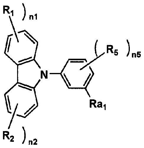
- A represents an atomic group necessary to form an aromatic hydrocarbon ring or an aromatic heterocyclic ring
- B represents a 5-membered nitrogen-containing aromatic heterocyclic ring or a 5-membered nitrogen-containing atom.
- M represents Ir or Pt.
- Ra represents an alkyl group, an alkenyl group, an alkynyl group, a cycloalkyl group, an aromatic group
- R, R and R are each a hydrogen atom
- nl, n2, and n5 each represents an integer of 0 to 4.
- Ra represents a hydrogen atom, an alkyl group, an alkenyl group, an alkynyl group, a cycloalkyl group, an aromatic hydrocarbon group, an aromatic heterocyclic group or a heterocyclic group
- Rb and Rc each represent hydrogen
- A1 represents an atom or a substituent
- A1 represents an atomic group necessary to form an aromatic hydrocarbon ring or an aromatic heterocycle
- M represents Ir or Pt.
- Ra represents an alkyl group, an alkenyl group, an alkynyl group, a cycloalkyl group, an aromatic hydrocarbon group, an aromatic heterocyclic group or a heterocyclic group
- Rb, Rc, Rb and Rc are Each A 1 represents a hydrogen atom or a substituent, A 1 represents an atomic group necessary for forming an aromatic hydrocarbon ring or an aromatic heterocyclic ring, and M represents Ir or Pt.
- Ra represents an alkyl group, an alkenyl group, an alkynyl group, a cycloalkyl group, an aromatic hydrocarbon group, an aromatic heterocyclic group or a heterocyclic group
- Rb and Rc each represents a hydrogen atom.
- A1 represents an atomic group necessary for forming an aromatic hydrocarbon ring or an aromatic heterocycle
- M represents Ir or Pt.
- R to R, R and R each represent a substituent
- nl to n4 represent 0 to 4
- n6 and n7 represent 0
- a display device comprising the organic electoluminescence device according to any one of 1 to 10 above.
- An illuminating device comprising the organic electoluminescence element according to any one of 1 to 10 above.
- a display device comprising the illumination device as described in 12 above and a liquid crystal element as display means.
- the invention's effect [0041] According to the present invention, it was possible to provide an organic EL element having a controlled emission wavelength, a high emission efficiency, and a long emission lifetime, and a lighting device and a display apparatus using the organic EL element. .
- FIG. 1 is a schematic view showing an example of a display device composed of organic EL elements.
- FIG. 2 is a schematic diagram of display unit A.
- FIG. 3 is an equivalent circuit diagram of a drive circuit constituting a pixel.
- FIG. 4 is a schematic diagram of a passive matrix display device.
- FIG. 5 is a schematic view of a lighting device.
- FIG. 6 is a schematic diagram of a lighting device.
- the present inventors have described a guest compound having a partial structure represented by the general formula (AA) (also referred to as a luminescent dopant) and a host compound represented by the general formula (1).
- AA general formula
- a host compound represented by the general formula (1) When an organic EL device was designed in combination with a compound and containing both of them in the light emitting layer, it was found to exhibit high external extraction efficiency and good light emission lifetime. It was also found that a highly efficient image display device and lighting device can be obtained by using the organic EL device of the present invention.
- the host compound represented by the general formula (1) according to the present invention will be described.
- the host compound is preferably a compound represented by the general formula (1), and the host compound represented by the general formula (1) is preferably the general formula (2). Or the compound represented by (3) is more preferable.
- examples of the alkyl group represented by Ra include, for example, a methylol group,
- examples of the alkenyl group represented by Ra include a bur group and an aryl group.
- examples of the alkynyl group represented by Ra include an ethul group
- examples of the cycloalkyl group represented by Ra include cyclopent A til group, a cyclohexyl group, etc. are mentioned. Further, these groups may further have substituents represented by R, R, R, etc. in the general formula (1) described later.
- an aromatic hydrocarbon group represented by Ra aromatic carbocyclic group, aryl
- phenyl group trinole group, azulenyl group, anthranyl group, phenanthrinole group, pyrenyl group, chrysenyl group, naphthacenyl group, o_terphenyl group, m_ terphenyl group, p-terphenyl group, and acenaphthyl Group, coronenyl group, fluorenyl group, perylenyl group and the like. Further, these groups may further have substituents represented by R, R, R and the like in the general formula (1) described later.
- examples of the aromatic heterocyclic group represented by Ra include a pyrrolyl group.
- Furyl group chenyl group, pyridyl group, pyridazinyl group, pyrimidinyl group, pyridyl group, triazinyl group, indolyl group, indolizinyl group, imidazolyl group, pyrazolyl group, thiazolyl group, thiadiazinyl group, oxadiazolyl group, benzoquinolinyl group, thiadiazolyl group, Quinolinyl group, quinazolinyl group, oxadiazolyl group, benzoquinolinyl group, thiadiazolyl group, pyro-thiazolyl group, pyrrolopyridazinyl group, tetrazolyl group, oxazolyl group, carbazolyl group, force noreborinole group, diazacarbazolyl group (Indicates one in which one of the carbon atoms constituting the carboline ring of the carbolinyl group,
- examples of the heterocyclic group represented by Ra include a pyrrolidinole group, an imi
- Examples thereof include a dazolidyl group, a morpholyl group, and an oxazolidinole group. Further, these groups further have substituents represented by R, R, R, etc. in the general formula (1) described later.
- each of the substituents represented by R, R, and R includes an alkyl group
- Aromatic heterocyclic groups eg, furyl, chenyl, pyridyl, pyridazinyl, pyrimidinyl, birazinyl, triazinyl, imidazolyl, pyrazolyl, thiazolyl, quinazolinyl, phthalazinyl, etc.
- Heterocyclic groups for example, pyrrolidinole group, imidazolidyl group, morpholyl group, oxazolidyl group, etc.
- alkoxy groups for example, methoxy group, ethoxy group, propyloxy group, pentyloxy group, hexynoleoxy group, octyloxy group, dodecyloxy group, etc.
- Cycloalkoxyl groups eg, cyclopentyloxy group, cyclohexyloxy group, etc.
- aryloxy groups eg, phenoxy group, naphthy
- a and A1 each represents an atomic group necessary for forming an aromatic hydrocarbon ring or an aromatic heterocycle.
- the aromatic hydrocarbon ring includes a benzene ring, a biphenyl ring, a naphthalene ring, an azulene ring, an anthracene ring, a phenanthrene ring, a pyrene ring, a thalylene ring, a naphthacene ring, a triphenylene ring, an o-terphenyl ring, m-terphenyl ring, p-terphenyl ring, acenaphthene ring, coronene ring, fluorene ring, fluoranthrene ring, naphthacene ring, pentacene ring, perylene ring, pentaphen ring, pin Sen ring, pyrene ring,
- Oxadiazole ring triazole ring, imidazole ring, pyrazole ring, thiazole ring, indole ring, benzimidazole ring, benzothiazole ring, benzoxazole ring, quinoxaline ring, quinazoline ring, phthalazine ring, force rubazole ring, carboline ring, And diaza-force rubazole ring (showing a ring in which one of the carbon atoms of the hydrocarbon ring constituting the carboline ring is further substituted with a nitrogen atom).
- Ra is an alkyl group, an alkenyl group, an alkynyl group, a cycloalkyl group, an aromatic hydrocarbon group, an aromatic heterocyclic group.
- Rb, Rc, Rb, Rc represents a hydrogen atom or a substituent, and Ra represents the above general formula (
- Rb, Rc, Rb, and Rc are the same as those of Ra in 1) above.
- Each of the structures represented by the general formulas (AA), (A), (B), or (C) is a partial structure.
- a corresponding ligand is required.
- it is also called a halogen atom (for example, fluorine atom, chlorine atom, bromine atom or iodine atom), aromatic hydrocarbon group (aromatic carbocyclic group, aryl group, etc., for example, phenyl group, p Chlorophenyl group, mesityl group, tolyl group, xylyl group, biphenyl group, naphthyl group, anthryl group, phenanthryl group, etc.), alkyl group (for example, methyl group, ethyl group, isopropyl group, hydroxyethyl group, methoxymethyl group, Trifluoromethyl group, tbutyl group, etc.), alkyloxy group, aryloxy group, alkylthio group, arylthio group, aromatic hetero
- M represents Ir or Pt, and Ir is particularly preferable.
- a tris body having a completed structure with three partial structures of the general formulas (A) to (C) is preferred.
- examples of the compound having a partial structure represented by the above (AA), (A), (B) or (C) of the guest compound (also referred to as a luminescent dopant) according to the present invention will be given. The present invention is not limited to these.
- an electrode material made of a metal, an alloy, an electrically conductive compound, or a mixture thereof having a high work function (4 eV or more) is preferably used.
- electrode materials include metals such as Au, and conductive transparent materials such as Cul, indium tinoxide (ITO), SnO, and ZnO. IDIX ⁇ (In O—Zn ⁇ ) etc.
- amorphous material capable of producing a transparent conductive film may be used.
- these electrode materials can be formed into a thin film by vapor deposition or sputtering, and a pattern of the desired shape can be formed by a single photolithography method. As described above, a pattern may be formed through a mask having a desired shape when the electrode material is deposited or sputtered.
- the transmittance be greater than 10%
- the sheet resistance as the anode is preferably several hundred ⁇ / mouth or less.
- the film thickness is a force depending on the material. Usually, 10 to 1000 nm, preferably 10 to 200 nm is selected.
- the cathode a material having a low work function (4 eV or less) metal (referred to as an electron injecting metal), an alloy, an electrically conductive compound, and a mixture thereof as an electrode material is used.
- electrode materials include sodium, sodium-potassium alloy, magnet Sum, lithium, magnesium / copper mixture, magnesium / silver mixture, magnesium / aluminum mixture, magnesium / indium mixture, aluminum / aluminum oxide (Al 2 O) mixture, indium, lithium / aluminum mixture, rare earth metal, etc.
- a mixture of an electron injecting metal and a second metal which is a stable metal having a larger work function than this for example, a magnesium / silver mixture, Magnesium / aluminum mixture, magnesium / indium mixture, aluminum / aluminum oxide (Al 2 O) mixture, lithium /
- the cathode can be produced by forming a thin film of these electrode materials by a method such as vapor deposition or sputtering.
- the sheet resistance as the cathode is preferably several hundred ⁇ / mouth or less, and the film thickness is usually selected in the range of 10 nm to 5 zm, preferably 50 nm to 200 nm.
- the anode or the cathode of the organic EL element is transparent or translucent, it is convenient to improve the emission luminance.
- a transparent or translucent cathode is manufactured by forming the above metal on the cathode with a film thickness of 1 nm to 20 nm and then forming the conductive transparent material mentioned in the description of the anode thereon. By applying this, it is possible to produce a device in which both the anode and the cathode are transparent.
- the injection layer is provided as necessary, and has an electron injection layer and a hole injection layer, and as described above, exists between the anode and the light emitting layer or hole transport layer and between the cathode and the light emitting layer or electron transport layer. May be.
- the injection layer is a layer provided between the electrode and the organic layer in order to lower the driving voltage and improve the light emission luminance.
- One anode buffer layer (hole injection layer) is disclosed in JP-A-9-45479 and 9-260062. The details are also described in the publications and publications of the publications Nos. 8-288069, and specific examples include a phthalocyanine buffer layer represented by copper phthalocyanine, an oxide buffer layer represented by vanadium oxide, an amorphous layer. Examples thereof include a carbon buffer layer, and a polymer buffer layer using a conductive polymer such as polyaniline (emeraldine) or polythiophene.
- the details of the cathode buffer layer are also described in JP-A-6-325871, JP-A-9-17574, and JP-A-10-74586.
- a metal buffer layer represented by strontium or aluminum an alkali metal compound buffer layer represented by lithium fluoride, an alkaline earth metal compound buffer layer represented by magnesium fluoride, and an oxide represented by aluminum oxide.
- the buffer layer (injection layer) should be a very thin film, although the film thickness is preferably in the range of 0.1 nm to 5 ⁇ m, depending on the desired material.
- Blocking layer hole blocking layer, electron blocking layer >>
- the blocking layer is provided as necessary in addition to the basic constituent layer of the organic compound thin film.
- Japanese Laid-Open Patent Publication Nos. 11-204258 and 11-204359, and “Organic EL devices and their forefront of industrialization” (published on November 30, 1998 by NTT Corporation), page 237 There is a hole blocking layer described in the above.
- the hole blocking layer is an electron transporting layer in a broad sense, and is made of a hole blocking material that has a function of transporting electrons and has a remarkably small ability to transport holes. The probability of recombination of electrons and holes can be improved by blocking.
- the hole blocking layer of the organic EL device of the present invention is provided adjacent to the light emitting layer.
- the hole blocking material of the hole blocking layer it is preferable to include the compound according to the present invention described above as the hole blocking material of the hole blocking layer. As a result, it is possible to achieve an organic EL device with even higher luminous efficiency. Further, the lifetime can be further increased.
- the electron blocking layer is a hole transport layer in a broad sense, and is made of a material having a function of transporting holes and a very small ability to transport electrons, and transporting electrons while transporting holes. By blocking, the recombination probability of electrons and holes can be improved.
- the light emitting layer according to the present invention is a layer that emits light by recombination of electrons and holes injected from the electrode, the electron transport layer, or the hole transport layer, and the light emitting portion is within the layer of the light emitting layer. May be the interface between the light emitting layer and the adjacent layer.
- the above-mentioned host compound and a light-emitting dopant are contained in the light-emitting layer of the present invention. Preference is given to using the compounds according to the invention. Thereby, the luminous efficiency can be further increased. Further, as the host compound, a compound other than the compound according to the present invention may be contained.
- the host compound is a compound having a phosphorescence quantum yield power of less than 0.01 for phosphorescence emission at room temperature (25 ° C.) among the compounds contained in the light emitting layer. Defined.
- a plurality of known host compounds may be used in combination. By using multiple types of host compounds, it is possible to adjust the movement of charges, and the organic EL device can be made highly efficient. Further, by using a plurality of kinds of light emitting dopants, it is possible to mix different light emission, and thereby any light emission color can be obtained. White light emission can be achieved by adjusting the type and doping amount of the luminescent dopant, and it can also be applied to lighting and backlighting.
- the light emitting layer may further contain a host compound having a fluorescence maximum wavelength as a host compound.
- a host compound having a fluorescence maximum wavelength is a compound having a high fluorescence quantum yield in a solution state.
- the fluorescence quantum yield is preferably 10% or more, particularly preferably 30% or more.
- Specific host compounds having a maximum fluorescence wavelength include coumarin dyes, pyran dyes, cyanine dyes, croconium dyes, squalium dyes, oxobenzanthracene dyes, fluorescein dyes, rhodamine dyes, Examples include pyrylium dyes, perylene dyes, stilbene dyes, and polythiophene dyes.
- the fluorescence quantum yield can be measured by the method described in the third edition of Experimental Chemistry Course 7, Spectroscopy II, page 362 (1992 edition, Maruzen).
- the guest compound according to the present invention (also referred to as a light-emitting dopant) is a compound in which light emission from an excited triplet is observed, is a compound that emits phosphorescence at room temperature (25 ° C), and has a phosphorescence quantum yield.
- the phosphorescence quantum yield is preferably 0.1 or more.
- the phosphorescence quantum yield can be measured by the method described in the 4th edition, Experimental Chemistry Course 7, Spectroscopy II, page 398 (1992 edition, Maruzen). Although the phosphorescence quantum yield in a solution can be measured using various solvents, the guest compound according to the present invention can be measured in any solvent so long as the phosphorescence quantum yield is achieved. ,.
- There are two types of light emission from guest compounds and one of them is the recombination of carriers on the host compound to which carriers are transported, and the excited state of the host compound is generated.
- the energy transfer type in which the energy is transferred to the guest compound to obtain light emission from the guest compound, and the other is the carrier trap, which is a carrier trap, which is a key on the guest compound.
- the excited state energy of the guest compound is higher than the excited state energy of the host compound, in which the carrier recombination occurs and light emission from the guest compound is obtained. Low is a condition.
- the phosphorescence emission maximum wavelength of the guest compound is not particularly limited. In principle, a central metal, a ligand, a substituent of the ligand, and the like are selected. However, it is preferable that the phosphorescence emission wavelength of the guest compound has a maximum phosphorescence emission wavelength of 380 to 480 nm. Luminous efficiency can be further increased with such blue phosphorescent organic EL devices and white phosphorescent organic EL devices.
- the light-emitting layer can be formed by forming the above compound by a known thin film method such as a vacuum deposition method, a spin coating method, a casting method, an LB method, an ink jet method, or the like.
- the thickness of the light emitting layer is not particularly limited, but is usually selected in the range of 5 nm to 5 zm, preferably 5 to 200 nm.
- This luminescent layer contains one or two of these luminescent dopants and host compounds. It may be a single layer structure composed of the above, or may be a laminated structure composed of a plurality of layers having the same composition or different compositions.
- the hole transport layer is made of a hole transport material having a function of transporting holes.
- a hole injection layer and an electron blocking layer are also included in the hole transport layer.
- the hole transport layer can be provided as a single layer or a plurality of layers.
- the hole transport material has any of the power of hole injection or transport and electron barrier property, and may be either organic or inorganic.
- triazole derivatives oxadiazole derivatives, imidazole derivatives, polyarylalkane derivatives, virazoline derivatives and pyrazolone derivatives, phenylenediamine derivatives, arylamine derivatives, amino-substituted chalcone derivatives, oxazole derivatives, styrylanthracene derivatives, fluorenone derivatives, hydrazone derivatives
- Examples thereof include stilbene derivatives, silazane derivatives, aniline copolymers, and conductive polymer oligomers, particularly thiophene oligomers.
- Typical examples of aromatic tertiary amine compounds and styrylamine compounds include N, N, N ', N' —tetraphenyl 4, ⁇ '— diaminophenyl; ⁇ , N' — diphenylol ⁇ , ⁇ '— Bis (3-methylphenyl) 1 [1, 1' — Biphenyl] 1, 4, 4 '— Diamine (TPD); 2, 2-bis (4-di 1 ⁇ -tolylaminophenyl) Propane; 1, 1-bis (4-di- ⁇ -triraminophenyl) cyclohexane; ⁇ , ⁇ , ⁇ ', N r —tetra-p-tolyl-4,4'-diaminobiphenyl; 1, 1— Bis (4-di-p-tolylaminophenyl) 1-4-phenyl hexane; bis (4-dimethylamino-2-methylphenyl) phenylmethane
- a polymer material in which these materials are introduced into a polymer chain or these materials are used as a polymer main chain can also be used.
- inorganic compounds such as P-type_Si and p-type_SiC can also be used as hole injection materials and hole transport materials.
- the hole transport layer is formed by thinning the hole transport material by a known method such as a vacuum deposition method, a spin coating method, a casting method, a printing method including an ink jet method, or an LB method. Can be formed.
- the film thickness of the hole transport layer is not particularly limited, but is usually about 5 ⁇ to 5 ⁇ , preferably 5 to 200 nm.
- This hole transport layer may have a single layer structure composed of one or more of the above materials.
- the electron transport layer is made of a material having a function of transporting electrons, and in a broad sense, an electron injection layer and a hole blocking layer are also included in the electron transport layer.
- the electron transport layer can be provided as a single layer or a plurality of layers.
- any material having a function of transmitting electrons injected from the electrode to the light-emitting layer can be used by selecting any intermediate force of a conventionally known compound.
- nitrogen substituted fluorene can be used.
- a thiadiazole derivative in which the oxygen atom of the oxadiazole ring is replaced with a sulfur atom.
- a quinoxaline derivative having a quinoxaline ring known as an electron withdrawing group can also be used as an electron transporting material.
- a polymer material in which these materials are introduced into a polymer chain or these materials are used as a polymer main chain can also be used.
- metal complexes of 8_quinolinol derivatives such as tris (8-quinolinol) aluminum (Alq), tris (5,7-dichloro-1-8-quinolinol) aluminum, tris (5,7-dibu Lomo 8_quinolinol) aluminum, tris (2-methyl_8_quinolinol) aluminum, tris (5-methyl_8_quinolinol) aluminum, bis (8-quinolinol) zinc (Zn q), etc., and their metal complexes Metal complexes in which the central metal is replaced with In, Mg, Cu, Ca, Sn, Ga, or Pb can also be used as electron transport materials.
- metal free or metal phthalocyanine, or those having terminal ends substituted with an alkyl group or a sulfonic acid group can be preferably used as the electron transporting material.
- the distyrylvirazine derivative exemplified as the material of the light emitting layer can also be used as an electron transport material, and, like the hole injection layer and the hole transport layer, n-type—Si, n-type—SiC, etc. These inorganic semiconductors can also be used as electron transport materials.
- the electron transport layer is formed by thinning the electron transport material by a known method such as a vacuum deposition method, a spin coating method, a casting method, a printing method including an ink jet method, or an LB method. can do.
- a vacuum deposition method such as a vacuum deposition method, a spin coating method, a casting method, a printing method including an ink jet method, or an LB method.
- a vacuum deposition method such as a vacuum deposition method, a spin coating method, a casting method, a printing method including an ink jet method, or an LB method.
- a there is no restriction
- the electron transport layer may have a single layer structure composed of one or more of the above materials.
- the organic EL device of the present invention is preferably formed on a substrate.
- the substrate (hereinafter also referred to as a substrate, substrate, support, etc.) that can be used in the organic EL device of the present invention is not particularly limited in the type of glass, plastic, etc., and may be transparent. Although there is no particular limitation, examples of the substrate that is preferably used include glass, quartz, and a light-transmitting resin film. A particularly preferable substrate is a resin film capable of imparting flexibility to the organic EL element.
- Examples of the resin film include polyethylene terephthalate (PET), polyethylene naphthalate (PEN), polyethersulfone (PES), polyetherimide, and polyether.
- Examples include films made of ether ketone, polyphenylene sulfide, polyarylate, polyimide, polycarbonate (PC), cellulose triacetate (TAC), cellulose acetate propionate (CAP), and the like.
- an inorganic or organic film or a hybrid film of both is formed on the surface of the resin film.
- the external extraction efficiency at room temperature of light emission of the organic EL device of the present invention is 1. / 0 is preferably from and this is preferred instrument is more than five. / 0 or more.
- the external extraction quantum efficiency (%) the number of photons emitted outside the organic EL element / the number of electrons XI 00 flowed to the organic EL element.
- a hue improvement filter such as a color filter may be used in combination, or a color conversion filter that converts the emission color from the organic EL element into multiple colors using a phosphor may be used in combination.
- a color conversion filter When a color conversion filter is used, the maximum light emission of the organic EL element is preferably 480 nm or less.
- a desired electrode material for example, a thin film made of an anode material is formed on a suitable substrate by a method such as vapor deposition or sputtering so as to have a thickness of 1 ⁇ m or less, preferably 10 nm to 200 nm.
- organic compound thin films of a hole injection layer, a hole transport layer, a light emitting layer, an electron transport layer, an electron injection layer, and a hole blocking layer, which are organic EL element materials, are formed thereon.
- the organic compound thin film can be deposited by a vapor deposition method or a wet process.
- the depositing conditions thereof are varied according to kinds of materials used, generally boat temperature 50 ° C ⁇ 450 ° C, vacuum degree of 10- 6 to 10-2 Pa, deposition rate 0 OlnmZ seconds to 50 mm / sec, substrate temperature—50 ° C to 300 ° C, film thickness 0.1 mm to 5 xm, preferably 5 nm to 200 nm.
- a thin film made of a cathode material is formed thereon with a thickness of 1 ⁇ m or less, preferably in the range of 50 nm to 200 nm, for example, by a method such as vapor deposition or sputtering.
- a desired organic EL device can be obtained.
- the organic EL element is preferably manufactured from the hole injection layer to the cathode consistently by a single evacuation, but it may be taken out halfway and subjected to different film forming methods. At that time, it is necessary to consider that the work is performed in a dry inert gas atmosphere.
- the multicolor display device of the present invention is provided with a shadow mask only at the time of forming a light emitting layer, and the other layers are common, so there is no need for patterning such as a shadow mask.
- a film can be formed by a method, an inkjet method, a printing method, or the like.
- the method is not limited, but the vapor deposition method, the ink jet method, and the printing method are preferable.
- patterning using a shadow mask is preferred.
- the order of production may be reversed, and the cathode, the electron injection layer, the electron transport layer, the light emitting layer, the hole transport layer, the hole injection layer, and the anode may be produced in this order.
- a DC voltage is applied to the multicolor display device thus obtained, light emission can be observed by applying a voltage of about 2 V to 40 V with the anode as + and the cathode as one polarity.
- An alternating voltage may be applied.
- the AC waveform to be applied is arbitrary.
- the display device of the present invention can be used as a display device, a display, and various light emission sources.
- Display devices and displays can be displayed in full color by using three types of organic EL elements that emit blue, red, and green light.
- Examples of display devices and displays include televisions, personal computers, mopile devices, AV devices, character broadcast displays, and information displays in automobiles.
- the driving method when used as a display device for reproducing moving images which may be used as a display device for reproducing still images or moving images, may be either a simple matrix (passive matrix) method or an active matrix method.
- the lighting device of the present invention includes household lighting, interior lighting, clock and liquid crystal backlights, signboard advertisements, traffic lights, light sources of optical storage media, light sources of electrophotographic copying machines, light sources of optical communication processors, light Examples include, but are not limited to, the light source of the sensor.
- the organic EL element of the present invention may be used as an organic EL element having a resonator structure.
- the purpose of using an organic EL element having such a resonator structure includes a light source of an optical storage medium, a light source of an electrophotographic copying machine, a light source of an optical communication processor, a light source of an optical sensor, etc. Not. Further, it may be used for the above application by causing laser oscillation.
- the organic EL device of the present invention may be used as a kind of lamp such as an illumination or exposure light source, a projection device that projects an image, or a type that directly observes a still image or a moving image. It may be used as a display device (display). When used as a display device for video playback, either the simple matrix (passive matrix) method or the active matrix method may be used. Alternatively, a full-color display device can be manufactured by using three or more organic EL elements of the present invention having different emission colors. Alternatively, it is also possible to make a single color emission color, for example, white emission, into a BGR using a color filter to achieve full color. Furthermore, it is possible to convert the organic EL emission color to other colors using a color conversion filter, and in this case, the organic EL emission max is preferably 480 nm or less.
- FIG. 1 is a schematic view showing an example of a display device composed of organic EL elements.
- FIG. 2 is a schematic diagram of a display such as a mobile phone that displays image information by light emission of an organic EL element.
- the display 1 includes a display unit A having a plurality of pixels, a control unit B that performs image staging of the display unit A based on image information, and the like.
- the control unit B is electrically connected to the display unit A, and sends a scanning signal and an image data signal to each of the plurality of pixels based on image information from the outside. Sequentially emit light according to the image data signal, scan the image, and display the image information on the display unit A.
- FIG. 2 is a schematic diagram of the display unit A.
- the display unit A includes a wiring unit including a plurality of scanning lines 5 and data lines 6, and a plurality of images on the substrate. Element 3 etc.
- the main members of the display unit A will be described below.
- FIG. 2 shows a case where the light emitted from the pixel 3 is extracted in the direction of the white arrow (downward).
- the scanning line 5 and the plurality of data lines 6 in the wiring portion are each made of a conductive material, and the scanning line 5 and the data line 6 are orthogonal to each other in a grid pattern and are connected to the pixel 3 at the orthogonal position. (Details not shown).
- the pixel 3 When a scanning signal is applied from the scanning line 5, the pixel 3 receives an image data signal from the data line 6 and emits light according to the received image data.
- Full color display is possible by appropriately arranging pixels in the red region, the green region, and the blue region on the same substrate.
- FIG. 3 is a schematic diagram of a pixel.
- the pixel includes an organic EL element 10, a switching transistor 11, a driving transistor 12, a capacitor 13, and the like.
- Full-color display can be performed by using organic EL elements of red, green, and blue light emission as organic EL elements 10 in a plurality of pixels and arranging them on the same substrate.
- an image data signal is applied from the control unit B to the drain of the switching transistor 11 via the data line 6.
- a scanning signal is applied from the control unit B to the gate of the switching transistor 11 via the scanning line 5
- the driving of the switching transistor 11 is turned on, and the image data signal applied to the drain is transferred to the capacitor 13 and the driving transistor. It is transmitted to the gate of the star 12.
- the capacitor 13 is charged according to the potential of the image data signal, and the drive of the drive transistor 12 is turned on.
- the drive transistor 12 has a drain connected to the power supply line 7 and a source connected to the electrode of the organic EL element 10, and the organic EL element is connected from the power supply line 7 according to the potential of the image data signal applied to the gate. Current is supplied to element 10.
- the driving of the switching transistor 11 is turned off. Even when the driving of the switching transistor 11 is turned off, the capacitor 13 holds the potential of the charged image data signal.
- the organic EL element 10 continues to emit light until the next driving signal is applied, while the driving state is kept on.
- the driving transistor 12 is driven according to the potential of the next image data signal synchronized with the scanning signal, and the organic EL element 10 emits light.
- the organic EL element 10 emits light by providing a switching transistor 11 and a driving transistor 12 which are active elements for the organic EL elements 10 of each of the plurality of pixels, and the organic EL elements of each of the plurality of pixels 3.
- Element 10 is emitting light.
- Such a light emitting method is called an active matrix method.
- the light emission of the organic EL element 10 may be light emission of a plurality of gradations by a multi-value image data signal having a plurality of gradation potentials, or a predetermined light emission amount of the binary image data signal. It may be on or off.
- the potential of the capacitor 13 can be maintained until the next scanning signal is applied, or can be discharged immediately before the next scanning signal is applied. .
- the present invention not only the active matrix method described above, but also a passive matrix light emission drive in which the organic EL element emits light according to the data signal only when the scanning signal is scanned.
- FIG. 4 is a schematic diagram of a display device using a passive matrix method.
- a plurality of scanning lines 5 and a plurality of image data lines 6 are provided in a grid pattern so as to face each other with the pixel 3 interposed therebetween.
- the pixel 3 connected to the applied scanning line 5 emits light according to the image data signal.
- the passive matrix method can reduce the manufacturing cost of the active element in addition to pixel 3.
- the material according to the present invention can also be applied to an organic EL element that emits substantially white light as a lighting device.
- a plurality of light-emitting materials simultaneously emit a plurality of light-emitting colors to obtain white light emission by color mixing.
- the combination of multiple emission colors may include three emission maximum wavelengths of the three primary colors of blue, green, and blue, or two using the relationship of complementary colors such as blue and yellow, blue green and orange, etc. The thing containing the light emission maximum wavelength may be used.
- a combination of light-emitting materials for obtaining a plurality of emission colors includes a plurality of phosphorescences or Any of a combination of a plurality of fluorescent materials (luminescent dopants), a combination of a fluorescent material or a phosphorescent material, and a dye material that emits light of the light emitting material power as excitation light may be used.
- a method of combining a plurality of light emitting dopants is preferable.
- the layer structure of the organic electoluminescence device for obtaining a plurality of emission colors includes a method in which a plurality of emission dopants are present in one emission layer, a plurality of emission layers, and each emission Examples thereof include a method in which dopants having different emission wavelengths are present in the layer, and a method in which minute pixels emitting light of different wavelengths are formed in a matrix.
- patterning may be performed by a metal mask, an ink jet printing method, or the like as needed during film formation.
- a metal mask In the case of patterning, only the electrode may be patterned, the electrode and the light emitting layer may be patterned, or the entire element layer may be patterned.
- the light emitting material used for the light emitting layer is not particularly limited.
- the light emitting material according to the present invention is adapted so as to conform to a wavelength range corresponding to CF (color filter) characteristics.
- CF color filter
- the light-emitting organic EL element of the present invention that emits white light can be used as various light-emitting light sources and lighting devices in addition to the display device and display, such as home lighting, interior lighting, and exposure light source. It is also useful as a kind of lamp and for display devices such as backlights for liquid crystal display devices.
- backlights for watches, signboard advertisements, traffic lights, light sources for optical storage media, light sources for electronic photocopiers, light sources for optical communication processors, light sources for optical sensors, and display devices are also required.
- the transparent support substrate with this ITO transparent electrode was ultrasonically cleaned with isopropyl alcohol and dried with dry nitrogen gas. UV ozone cleaning was performed for 5 minutes.
- This transparent support substrate is fixed to a substrate holder of a commercially available vacuum evaporation system, while 200 mg of NPD is placed in a molybdenum resistance heating boat, and 200 mg of CBP is used as a host compound in another resistance heating boat made of molybdenum.
- an electron transport layer that also serves as a hole blocking layer with a thickness of 10 nm is provided by energizing and heating the heating boat containing BCP and depositing it on the light emitting layer at a deposition rate of 0. Inm / sec. It was. Furthermore, the heating boat containing Alq is further energized and heated, and the deposition rate is 0. Inm / sec.
- an electron injection layer having a film thickness of 40 nm was further formed by vapor deposition on the electron transport layer.
- the substrate temperature at the time of deposition was room temperature.
- organic EL device 1-1 For the production of the organic EL device 1-1, use CBP as the host compound for the light-emitting layer by replacing the CBP with the compounds shown in Table 1 and use it as the light-emitting dopant for the light-emitting layer.
- Organic D except that D-1 is replaced with the compound shown in Table 1 as the luminescent dopant.
- the organic EL devices 1_1 to 1_20 fabricated as follows were evaluated and the results are shown in Table 1.
- the external extraction quantum efficiency (%) was measured when a constant current of 2.5 mA / cm 2 was applied in a dry nitrogen gas atmosphere at 23 ° C.
- a spectral radiance meter CS-1000 manufactured by Konica Minolta Sensing was used in the same manner.
- the measurement results of the external extraction quantum efficiency in Table 1 are expressed as relative values when the measured value of the organic EL element 11 is 100.
- the electrode of the transparent electrode substrate of Example 1 was patterned to 20 mm x 20 mm, and ⁇ -NPD was deposited to a thickness of 50 nm as a hole injecting / transporting layer as in Example 1, and then H
- the heated boat containing 1-1, the boat containing D-1 and the boat containing Ir-9 are energized independently, respectively, and the compound H-1 which is a host compound and D-1 which is a luminescent dopant.
- the deposition rate of Ir-9 was adjusted to 100: 5: 06, and deposition was performed to a thickness of 30 nm to provide a light emitting layer.
- BCP was deposited to a thickness of 10 nm to provide an electron transport layer. Furthermore, Alq was deposited at 40nm,
- An electron injection layer was provided.
- This element was sealed using a sealing can having the same method and the same structure as in Example 1 to fabricate a flat lamp.
- this flat lamp was energized, almost white light was obtained, indicating that it could be used as a lighting device. It was found that white light emission was obtained in the same manner even when the host compound was replaced with another compound according to the present invention.
- the organic EL device 13 of Example 1 was used as a blue light emitting device.
- a green light emitting device was produced in the same manner as in the organic EL device 13 of Example 1 except that the host compound was changed to CBP and the dopant was changed to Ir 1, and this was used as a green light emitting device.
- a red light emitting device was produced in the same manner as in the organic EL device 13 of Example 1, except that the host compound was changed to CBP and the dopant was changed to Ir 1, and this was used as a red light emitting device.
- FIG. 2 shows only a schematic view of the display portion A of the display device thus manufactured.
- a wiring portion including a plurality of scanning lines 5 and data lines 6 and a plurality of juxtaposed pixels 3 (emission color is a red region pixel, a green region pixel, a blue region pixel, etc.) And running the wiring section
- the saddle wire 5 and the plurality of data lines 6 are each made of a conductive material, and the scanning lines 5 and the data lines 6 are orthogonal to each other in a grid pattern and are connected to the pixels 3 at the orthogonal positions (details are not shown).
- the plurality of pixels 3 are driven by a formula that is an organic EL element and an active element corresponding to each emission color, and when a scanning signal is applied from the scanning line 5, the image data is transmitted from the data line 6. A signal is received, and light is emitted according to the received image data. In this manner, a full color display device was produced by appropriately juxtaposing the red, green, and blue pixels.
- each of the blue light emitting, green light emitting, and red light emitting organic EL elements produced in Example 3 was covered with a glass case to obtain a lighting device.
- the illuminating device could be used as a thin illuminating device that emits white light with high luminous efficiency and long emission life.
- FIG. 5 is a schematic view of the lighting device
- FIG. 6 is a cross-sectional view of the lighting device.
- the organic EL element 101 was covered with a glass cover 102.
- 105 is a cathode
- 106 is an organic EL layer
- 107 is a glass substrate with a transparent electrode.
- the glass cover 102 is filled with nitrogen gas 108 and a water catching agent 109 is provided.
Abstract
Description


Claims


Priority Applications (2)
| Application Number | Priority Date | Filing Date | Title |
|---|---|---|---|
| JP2007520029A JPWO2006132012A1 (ja) | 2005-06-09 | 2006-03-03 | 有機エレクトロルミネッセンス素子、照明装置及び表示装置 |
| GB0723474A GB2442885B (en) | 2005-06-09 | 2006-03-03 | Organic electroluminescence element, illuminator and display |
Applications Claiming Priority (2)
| Application Number | Priority Date | Filing Date | Title |
|---|---|---|---|
| JP2005-169227 | 2005-06-09 | ||
| JP2005169227 | 2005-06-09 |
Publications (1)
| Publication Number | Publication Date |
|---|---|
| WO2006132012A1 true WO2006132012A1 (ja) | 2006-12-14 |
Family
ID=37498221
Family Applications (1)
| Application Number | Title | Priority Date | Filing Date |
|---|---|---|---|
| PCT/JP2006/304064 WO2006132012A1 (ja) | 2005-06-09 | 2006-03-03 | 有機エレクトロルミネッセンス素子、照明装置及び表示装置 |
Country Status (4)
| Country | Link |
|---|---|
| US (3) | US8808874B2 (ja) |
| JP (4) | JPWO2006132012A1 (ja) |
| GB (2) | GB2442885B (ja) |
| WO (1) | WO2006132012A1 (ja) |
Cited By (3)
| Publication number | Priority date | Publication date | Assignee | Title |
|---|---|---|---|---|
| JP2007180147A (ja) * | 2005-12-27 | 2007-07-12 | Konica Minolta Holdings Inc | 有機エレクトロルミネッセンス素子材料、有機エレクトロルミネッセンス素子、表示装置及び照明装置 |
| JPWO2008035571A1 (ja) * | 2006-09-20 | 2010-01-28 | コニカミノルタホールディングス株式会社 | 有機エレクトロルミネッセンス素子 |
| JP2011256143A (ja) * | 2010-06-10 | 2011-12-22 | Fujifilm Corp | 特定構造のカルバゾール系化合物、並びにそれを用いた電荷輸送材料及び有機電界発光素子 |
Families Citing this family (21)
| Publication number | Priority date | Publication date | Assignee | Title |
|---|---|---|---|---|
| US8007927B2 (en) * | 2007-12-28 | 2011-08-30 | Universal Display Corporation | Dibenzothiophene-containing materials in phosphorescent light emitting diodes |
| WO2006132012A1 (ja) * | 2005-06-09 | 2006-12-14 | Konica Minolta Holdings, Inc. | 有機エレクトロルミネッセンス素子、照明装置及び表示装置 |
| JP5233081B2 (ja) * | 2006-05-17 | 2013-07-10 | コニカミノルタ株式会社 | 有機エレクトロルミネッセンス素子材料、有機エレクトロルミネッセンス素子、表示装置及び照明装置 |
| EP1918349A1 (en) * | 2006-10-12 | 2008-05-07 | SOLVAY (Société Anonyme) | Light-emitting material |
| US8120022B2 (en) * | 2007-07-27 | 2012-02-21 | Toray Industries, Inc. | Light emitting device material and light emitting device |
| KR100882911B1 (ko) * | 2007-08-16 | 2009-02-10 | 삼성모바일디스플레이주식회사 | 유기전계발광소자 및 그의 제조방법 |
| JP5267557B2 (ja) * | 2008-04-30 | 2013-08-21 | コニカミノルタ株式会社 | 有機エレクトロルミネッセンス素子、照明装置及び表示装置 |
| WO2010067746A1 (ja) * | 2008-12-08 | 2010-06-17 | コニカミノルタホールディングス株式会社 | 有機エレクトロルミネッセンス素子、表示装置、及び照明装置 |
| JP5561272B2 (ja) * | 2009-04-14 | 2014-07-30 | コニカミノルタ株式会社 | 有機エレクトロルミネッセンス素子 |
| US10243023B2 (en) | 2013-01-18 | 2019-03-26 | Universal Display Corporation | Top emission AMOLED displays using two emissive layers |
| US10580832B2 (en) | 2013-01-18 | 2020-03-03 | Universal Display Corporation | High resolution low power consumption OLED display with extended lifetime |
| US10229956B2 (en) | 2013-01-18 | 2019-03-12 | Universal Display Corporation | High resolution low power consumption OLED display with extended lifetime |
| US10304906B2 (en) | 2013-01-18 | 2019-05-28 | Universal Display Corporation | High resolution low power consumption OLED display with extended lifetime |
| US9590017B2 (en) | 2013-01-18 | 2017-03-07 | Universal Display Corporation | High resolution low power consumption OLED display with extended lifetime |
| US9385168B2 (en) * | 2013-01-18 | 2016-07-05 | Universal Display Corporation | High resolution low power consumption OLED display with extended lifetime |
| JP2014227399A (ja) * | 2013-05-24 | 2014-12-08 | 三星ディスプレイ株式會社Samsung Display Co.,Ltd. | アリールアミン誘導体及びそれを正孔輸送材料に用いた有機電界発光素子 |
| US10700134B2 (en) | 2014-05-27 | 2020-06-30 | Universal Display Corporation | Low power consumption OLED display |
| US10672995B2 (en) * | 2014-07-24 | 2020-06-02 | Samsung Electronics Co., Ltd. | Organometallic compound and organic light-emitting device including the same |
| US9818804B2 (en) | 2015-09-18 | 2017-11-14 | Universal Display Corporation | Hybrid display |
| US10263050B2 (en) | 2015-09-18 | 2019-04-16 | Universal Display Corporation | Hybrid display |
| US10797112B2 (en) | 2018-07-25 | 2020-10-06 | Universal Display Corporation | Energy efficient OLED TV |
Citations (9)
| Publication number | Priority date | Publication date | Assignee | Title |
|---|---|---|---|---|
| JP2004071380A (ja) * | 2002-08-07 | 2004-03-04 | Konica Minolta Holdings Inc | 有機エレクトロルミネッセンス素子及び表示装置 |
| JP2004178895A (ja) * | 2002-11-26 | 2004-06-24 | Konica Minolta Holdings Inc | 有機エレクトロルミネッセンス素子および表示装置 |
| JP2004178896A (ja) * | 2002-11-26 | 2004-06-24 | Konica Minolta Holdings Inc | 有機エレクトロルミネッセンス素子及び表示装置 |
| JP2004273128A (ja) * | 2003-03-05 | 2004-09-30 | Konica Minolta Holdings Inc | 有機エレクトロルミネッセンス素子 |
| JP2004273389A (ja) * | 2003-03-12 | 2004-09-30 | Konica Minolta Holdings Inc | 有機エレクトロルミネッセンス素子及び表示装置 |
| JP2004288380A (ja) * | 2003-03-19 | 2004-10-14 | Konica Minolta Holdings Inc | 有機エレクトロルミネッセンス素子 |
| JP2004311404A (ja) * | 2003-03-26 | 2004-11-04 | Konica Minolta Holdings Inc | 有機エレクトロルミネッセンス素子、照明装置および表示装置 |
| JP2004335427A (ja) * | 2002-11-26 | 2004-11-25 | Konica Minolta Holdings Inc | 有機エレクトロルミネッセンス素子及びそれを有する表示装置 |
| JP2005047811A (ja) * | 2003-07-29 | 2005-02-24 | Mitsubishi Chemicals Corp | 有機化合物、電荷輸送材料、有機電界発光素子材料および有機電界発光素子 |
Family Cites Families (33)
| Publication number | Priority date | Publication date | Assignee | Title |
|---|---|---|---|---|
| US20020022588A1 (en) * | 1998-06-23 | 2002-02-21 | James Wilkie | Methods and compositions for sealing tissue leaks |
| US6458475B1 (en) | 1999-11-24 | 2002-10-01 | The Trustee Of Princeton University | Organic light emitting diode having a blue phosphorescent molecule as an emitter |
| KR100840637B1 (ko) | 1999-12-01 | 2008-06-24 | 더 트러스티즈 오브 프린스턴 유니버시티 | 유기 led용 인광성 도펀트로서 l2mx 형태의 착물 |
| TW532048B (en) * | 2000-03-27 | 2003-05-11 | Idemitsu Kosan Co | Organic electroluminescence element |
| US6939624B2 (en) | 2000-08-11 | 2005-09-06 | Universal Display Corporation | Organometallic compounds and emission-shifting organic electrophosphorescence |
| WO2002015645A1 (en) | 2000-08-11 | 2002-02-21 | The Trustees Of Princeton University | Organometallic compounds and emission-shifting organic electrophosphorescence |
| GB0021513D0 (en) * | 2000-09-01 | 2000-10-18 | E2 One Uk Ltd | Method and system for dynamic web-page generation and computer-readable storage medium storing a program for performing the method |
| JP4086498B2 (ja) | 2000-11-29 | 2008-05-14 | キヤノン株式会社 | 金属配位化合物、発光素子及び表示装置 |
| JP4086499B2 (ja) | 2000-11-29 | 2008-05-14 | キヤノン株式会社 | 金属配位化合物、発光素子及び表示装置 |
| JP3812730B2 (ja) | 2001-02-01 | 2006-08-23 | 富士写真フイルム株式会社 | 遷移金属錯体及び発光素子 |
| JP4307000B2 (ja) | 2001-03-08 | 2009-08-05 | キヤノン株式会社 | 金属配位化合物、電界発光素子及び表示装置 |
| JP4438042B2 (ja) | 2001-03-08 | 2010-03-24 | キヤノン株式会社 | 金属配位化合物、電界発光素子及び表示装置 |
| JP4307001B2 (ja) | 2001-03-14 | 2009-08-05 | キヤノン株式会社 | 金属配位化合物、電界発光素子及び表示装置 |
| JP5135660B2 (ja) * | 2001-09-27 | 2013-02-06 | コニカミノルタホールディングス株式会社 | 有機エレクトロルミネッセンス素子 |
| US6863997B2 (en) | 2001-12-28 | 2005-03-08 | The Trustees Of Princeton University | White light emitting OLEDs from combined monomer and aggregate emission |
| EP1489155A4 (en) | 2002-03-22 | 2006-02-01 | Idemitsu Kosan Co | MATERIAL FOR ORGANIC ELECTROLUMINESCENT DEVICES AND ORGANIC ELECTROLUMINESCENT DEVICES PRODUCED WITH THIS MATERIAL |
| CN1656194A (zh) * | 2002-03-25 | 2005-08-17 | 出光兴产株式会社 | 用于有机电致发光元件的材料和应用该材料的有机电致发光元件 |
| JP2003317946A (ja) * | 2002-04-23 | 2003-11-07 | Konica Minolta Holdings Inc | 有機el素子及び有機el素子の製造方法 |
| US20060257684A1 (en) | 2002-10-09 | 2006-11-16 | Idemitsu Kosan Co., Ltd. | Organic electroluminescent device |
| EP2765174B1 (en) * | 2002-11-26 | 2018-05-30 | Konica Minolta Holdings, Inc. | Organic electroluminescent element, and display and illuminator |
| WO2004074399A1 (ja) * | 2003-02-20 | 2004-09-02 | Idemitsu Kosan Co., Ltd. | 有機エレクトロルミネッセンス素子用材料及びそれを用いた有機エレクトロルミネッセンス素子 |
| JP4590825B2 (ja) * | 2003-02-21 | 2010-12-01 | コニカミノルタホールディングス株式会社 | 白色発光有機エレクトロルミネッセンス素子 |
| JP4525190B2 (ja) * | 2003-06-09 | 2010-08-18 | 日立化成工業株式会社 | 金属配位化合物、ポリマー組成物、およびこれらを用いた有機エレクトロルミネセンス素子 |
| JP4203732B2 (ja) * | 2003-06-12 | 2009-01-07 | ソニー株式会社 | 有機電界発光材料、有機電界発光素子および含複素環イリジウム錯体化合物 |
| EP2336142B1 (en) * | 2003-07-22 | 2013-09-04 | Idemitsu Kosan Co., Ltd. | Iridium organic complex and electroluminescent device using same |
| JP4198654B2 (ja) | 2003-08-07 | 2008-12-17 | 三星エスディアイ株式会社 | イリジウム化合物及びそれを採用した有機電界発光素子 |
| JP4337475B2 (ja) * | 2003-08-27 | 2009-09-30 | 三菱化学株式会社 | 有機金属錯体、発光材料、および有機電界発光素子 |
| CN100335462C (zh) | 2003-09-05 | 2007-09-05 | 清华大学 | 咔唑衍生物及其在电致发光器件中的应用 |
| TWI245068B (en) * | 2003-11-18 | 2005-12-11 | Chi Mei Optoelectronics Corp | Iridium complex as light emitting material and organic light emitting diode device |
| JP2005169227A (ja) * | 2003-12-10 | 2005-06-30 | Showa Aircraft Ind Co Ltd | 溶剤回収装置 |
| US20060008670A1 (en) * | 2004-07-06 | 2006-01-12 | Chun Lin | Organic light emitting materials and devices |
| EP2271183B1 (en) | 2004-07-23 | 2015-03-18 | Konica Minolta Holdings, Inc. | Organic electroluminescent element, display and illuminator |
| WO2006132012A1 (ja) * | 2005-06-09 | 2006-12-14 | Konica Minolta Holdings, Inc. | 有機エレクトロルミネッセンス素子、照明装置及び表示装置 |
-
2006
- 2006-03-03 WO PCT/JP2006/304064 patent/WO2006132012A1/ja active Application Filing
- 2006-03-03 GB GB0723474A patent/GB2442885B/en active Active
- 2006-03-03 GB GB1104120A patent/GB2476003B/en active Active
- 2006-03-03 JP JP2007520029A patent/JPWO2006132012A1/ja active Pending
- 2006-06-01 US US11/444,590 patent/US8808874B2/en active Active
-
2010
- 2010-12-07 US US12/961,703 patent/US8728633B2/en active Active
- 2010-12-10 US US12/964,738 patent/US9428687B2/en active Active
-
2011
- 2011-12-08 JP JP2011268590A patent/JP2012109575A/ja active Pending
- 2011-12-08 JP JP2011268592A patent/JP5790463B2/ja active Active
-
2012
- 2012-12-03 JP JP2012264325A patent/JP5733294B2/ja active Active
Patent Citations (9)
| Publication number | Priority date | Publication date | Assignee | Title |
|---|---|---|---|---|
| JP2004071380A (ja) * | 2002-08-07 | 2004-03-04 | Konica Minolta Holdings Inc | 有機エレクトロルミネッセンス素子及び表示装置 |
| JP2004178895A (ja) * | 2002-11-26 | 2004-06-24 | Konica Minolta Holdings Inc | 有機エレクトロルミネッセンス素子および表示装置 |
| JP2004178896A (ja) * | 2002-11-26 | 2004-06-24 | Konica Minolta Holdings Inc | 有機エレクトロルミネッセンス素子及び表示装置 |
| JP2004335427A (ja) * | 2002-11-26 | 2004-11-25 | Konica Minolta Holdings Inc | 有機エレクトロルミネッセンス素子及びそれを有する表示装置 |
| JP2004273128A (ja) * | 2003-03-05 | 2004-09-30 | Konica Minolta Holdings Inc | 有機エレクトロルミネッセンス素子 |
| JP2004273389A (ja) * | 2003-03-12 | 2004-09-30 | Konica Minolta Holdings Inc | 有機エレクトロルミネッセンス素子及び表示装置 |
| JP2004288380A (ja) * | 2003-03-19 | 2004-10-14 | Konica Minolta Holdings Inc | 有機エレクトロルミネッセンス素子 |
| JP2004311404A (ja) * | 2003-03-26 | 2004-11-04 | Konica Minolta Holdings Inc | 有機エレクトロルミネッセンス素子、照明装置および表示装置 |
| JP2005047811A (ja) * | 2003-07-29 | 2005-02-24 | Mitsubishi Chemicals Corp | 有機化合物、電荷輸送材料、有機電界発光素子材料および有機電界発光素子 |
Cited By (4)
| Publication number | Priority date | Publication date | Assignee | Title |
|---|---|---|---|---|
| JP2007180147A (ja) * | 2005-12-27 | 2007-07-12 | Konica Minolta Holdings Inc | 有機エレクトロルミネッセンス素子材料、有機エレクトロルミネッセンス素子、表示装置及び照明装置 |
| JPWO2008035571A1 (ja) * | 2006-09-20 | 2010-01-28 | コニカミノルタホールディングス株式会社 | 有機エレクトロルミネッセンス素子 |
| JP5556014B2 (ja) * | 2006-09-20 | 2014-07-23 | コニカミノルタ株式会社 | 有機エレクトロルミネッセンス素子 |
| JP2011256143A (ja) * | 2010-06-10 | 2011-12-22 | Fujifilm Corp | 特定構造のカルバゾール系化合物、並びにそれを用いた電荷輸送材料及び有機電界発光素子 |
Also Published As
| Publication number | Publication date |
|---|---|
| JP5733294B2 (ja) | 2015-06-10 |
| JP2013102165A (ja) | 2013-05-23 |
| US8728633B2 (en) | 2014-05-20 |
| US20060280966A1 (en) | 2006-12-14 |
| GB201104120D0 (en) | 2011-04-27 |
| US20110073850A1 (en) | 2011-03-31 |
| JP2012109575A (ja) | 2012-06-07 |
| GB2442885A (en) | 2008-04-16 |
| GB2476003B (en) | 2011-09-14 |
| GB2442885B (en) | 2011-07-13 |
| JP2012109576A (ja) | 2012-06-07 |
| JPWO2006132012A1 (ja) | 2009-01-08 |
| US20110073851A1 (en) | 2011-03-31 |
| GB2476003A (en) | 2011-06-08 |
| GB0723474D0 (en) | 2008-01-09 |
| JP5790463B2 (ja) | 2015-10-07 |
| US9428687B2 (en) | 2016-08-30 |
| US8808874B2 (en) | 2014-08-19 |
Similar Documents
| Publication | Publication Date | Title |
|---|---|---|
| JP5733294B2 (ja) | 有機エレクトロルミネッセンス素子 | |
| JP5533652B2 (ja) | 白色発光有機エレクトロルミネッセンス素子、照明装置及び表示装置 | |
| JP5870782B2 (ja) | 有機エレクトロルミネッセンス素子、有機エレクトロルミネッセンス素子の製造方法、照明装置及び表示装置 | |
| JP5853964B2 (ja) | 有機エレクトロルミネッセンス素子、照明装置及び表示装置 | |
| WO2012096241A1 (ja) | 有機エレクトロルミネッセンス素子、照明装置及び表示装置 | |
| JP2011222650A (ja) | 有機エレクトロルミネッセンス素子、表示装置、及び照明装置 | |
| JP2007180148A (ja) | 有機エレクトロルミネッセンス素子材料、有機エレクトロルミネッセンス素子、表示装置及び照明装置 | |
| JP2006143845A (ja) | 有機エレクトロルミネッセンス素子用材料、有機エレクトロルミネッセンス素子、照明装置及び表示装置 | |
| WO2006013739A1 (ja) | 有機エレクトロルミネッセンス素子、照明装置及び表示装置 | |
| JP2013168552A (ja) | 有機エレクトロルミネッセンス素子、それが具備された表示装置及び照明装置 | |
| JP5353006B2 (ja) | 有機エレクトロルミネッセンス素子、液晶表示装置及び照明装置 | |
| WO2005062676A1 (ja) | 有機エレクトロルミネッセンス素子用材料、有機エレクトロルミネッセンス素子、照明装置および表示装置 | |
| JP5482313B2 (ja) | 有機エレクトロルミネッセンス素子、表示装置、及び照明装置 | |
| JP4552436B2 (ja) | 有機エレクトロルミネッセンス素子、表示装置及び照明装置 | |
| JP5055689B2 (ja) | 有機エレクトロルミネッセンス素子用材料、有機エレクトロルミネッセンス素子、照明装置および表示装置 | |
| JPWO2009008263A1 (ja) | 有機エレクトロルミネッセンス材料、有機エレクトロルミネッセンス素子、表示装置及び照明装置 | |
| JP2006080271A (ja) | 有機エレクトロルミネッセンス素子、照明装置及び表示装置 | |
| JP6011535B2 (ja) | 有機エレクトロルミネッセンス素子、照明装置、表示装置及び有機エレクトロルミネッセンス素子の製造方法 | |
| WO2006043440A1 (ja) | 有機エレクトロルミネッセンス素子、表示装置及び照明装置 | |
| JP5320881B2 (ja) | 有機エレクトロルミネッセンス素子、表示装置、照明装置及び有機エレクトロルミネッセンス素子材料 | |
| JP2006156635A (ja) | 有機エレクトロルミネッセンス素子及び表示装置 | |
| JP4968392B2 (ja) | 有機エレクトロルミネッセンス素子及び表示装置 | |
| JP4900521B2 (ja) | 有機エレクトロルミネッセンス素子及び表示装置 | |
| JP5833201B2 (ja) | 有機エレクトロルミネッセンス素子その製造方法、照明装置及び表示装置 | |
| JP5603195B2 (ja) | 有機エレクトロルミネッセンス素子その製造方法、照明装置及び表示装置 |
Legal Events
| Date | Code | Title | Description |
|---|---|---|---|
| 121 | Ep: the epo has been informed by wipo that ep was designated in this application | ||
| WWE | Wipo information: entry into national phase |
Ref document number: 2007520029 Country of ref document: JP |
|
| ENP | Entry into the national phase |
Ref document number: 0723474 Country of ref document: GB Kind code of ref document: A Free format text: PCT FILING DATE = 20060303 |
|
| WWE | Wipo information: entry into national phase |
Ref document number: 0723474.3 Country of ref document: GB |
|
| NENP | Non-entry into the national phase |
Ref country code: DE |
|
| 122 | Ep: pct application non-entry in european phase |
Ref document number: 06715147 Country of ref document: EP Kind code of ref document: A1 |