WO2006059542A1 - エポキシ樹脂組成物及び半導体装置 - Google Patents
エポキシ樹脂組成物及び半導体装置 Download PDFInfo
- Publication number
- WO2006059542A1 WO2006059542A1 PCT/JP2005/021658 JP2005021658W WO2006059542A1 WO 2006059542 A1 WO2006059542 A1 WO 2006059542A1 JP 2005021658 W JP2005021658 W JP 2005021658W WO 2006059542 A1 WO2006059542 A1 WO 2006059542A1
- Authority
- WO
- WIPO (PCT)
- Prior art keywords
- epoxy resin
- resin composition
- semiconductor
- weight
- semiconductor encapsulation
- Prior art date
- Legal status (The legal status is an assumption and is not a legal conclusion. Google has not performed a legal analysis and makes no representation as to the accuracy of the status listed.)
- Ceased
Links
Classifications
-
- H—ELECTRICITY
- H10—SEMICONDUCTOR DEVICES; ELECTRIC SOLID-STATE DEVICES NOT OTHERWISE PROVIDED FOR
- H10W—GENERIC PACKAGES, INTERCONNECTIONS, CONNECTORS OR OTHER CONSTRUCTIONAL DETAILS OF DEVICES COVERED BY CLASS H10
- H10W74/00—Encapsulations, e.g. protective coatings
- H10W74/40—Encapsulations, e.g. protective coatings characterised by their materials
- H10W74/47—Encapsulations, e.g. protective coatings characterised by their materials comprising organic materials, e.g. plastics or resins
- H10W74/473—Encapsulations, e.g. protective coatings characterised by their materials comprising organic materials, e.g. plastics or resins containing a filler
-
- C—CHEMISTRY; METALLURGY
- C08—ORGANIC MACROMOLECULAR COMPOUNDS; THEIR PREPARATION OR CHEMICAL WORKING-UP; COMPOSITIONS BASED THEREON
- C08L—COMPOSITIONS OF MACROMOLECULAR COMPOUNDS
- C08L61/00—Compositions of condensation polymers of aldehydes or ketones; Compositions of derivatives of such polymers
- C08L61/04—Condensation polymers of aldehydes or ketones with phenols only
- C08L61/06—Condensation polymers of aldehydes or ketones with phenols only of aldehydes with phenols
-
- C—CHEMISTRY; METALLURGY
- C08—ORGANIC MACROMOLECULAR COMPOUNDS; THEIR PREPARATION OR CHEMICAL WORKING-UP; COMPOSITIONS BASED THEREON
- C08L—COMPOSITIONS OF MACROMOLECULAR COMPOUNDS
- C08L63/00—Compositions of epoxy resins; Compositions of derivatives of epoxy resins
-
- C—CHEMISTRY; METALLURGY
- C08—ORGANIC MACROMOLECULAR COMPOUNDS; THEIR PREPARATION OR CHEMICAL WORKING-UP; COMPOSITIONS BASED THEREON
- C08L—COMPOSITIONS OF MACROMOLECULAR COMPOUNDS
- C08L9/00—Compositions of homopolymers or copolymers of conjugated diene hydrocarbons
- C08L9/02—Copolymers with acrylonitrile
-
- C—CHEMISTRY; METALLURGY
- C09—DYES; PAINTS; POLISHES; NATURAL RESINS; ADHESIVES; COMPOSITIONS NOT OTHERWISE PROVIDED FOR; APPLICATIONS OF MATERIALS NOT OTHERWISE PROVIDED FOR
- C09D—COATING COMPOSITIONS, e.g. PAINTS, VARNISHES OR LACQUERS; FILLING PASTES; CHEMICAL PAINT OR INK REMOVERS; INKS; CORRECTING FLUIDS; WOODSTAINS; PASTES OR SOLIDS FOR COLOURING OR PRINTING; USE OF MATERIALS THEREFOR
- C09D163/00—Coating compositions based on epoxy resins; Coating compositions based on derivatives of epoxy resins
-
- C—CHEMISTRY; METALLURGY
- C09—DYES; PAINTS; POLISHES; NATURAL RESINS; ADHESIVES; COMPOSITIONS NOT OTHERWISE PROVIDED FOR; APPLICATIONS OF MATERIALS NOT OTHERWISE PROVIDED FOR
- C09D—COATING COMPOSITIONS, e.g. PAINTS, VARNISHES OR LACQUERS; FILLING PASTES; CHEMICAL PAINT OR INK REMOVERS; INKS; CORRECTING FLUIDS; WOODSTAINS; PASTES OR SOLIDS FOR COLOURING OR PRINTING; USE OF MATERIALS THEREFOR
- C09D163/00—Coating compositions based on epoxy resins; Coating compositions based on derivatives of epoxy resins
- C09D163/08—Epoxidised polymerised polyenes
-
- H—ELECTRICITY
- H10—SEMICONDUCTOR DEVICES; ELECTRIC SOLID-STATE DEVICES NOT OTHERWISE PROVIDED FOR
- H10W—GENERIC PACKAGES, INTERCONNECTIONS, CONNECTORS OR OTHER CONSTRUCTIONAL DETAILS OF DEVICES COVERED BY CLASS H10
- H10W74/00—Encapsulations, e.g. protective coatings
- H10W74/01—Manufacture or treatment
-
- H—ELECTRICITY
- H10—SEMICONDUCTOR DEVICES; ELECTRIC SOLID-STATE DEVICES NOT OTHERWISE PROVIDED FOR
- H10W—GENERIC PACKAGES, INTERCONNECTIONS, CONNECTORS OR OTHER CONSTRUCTIONAL DETAILS OF DEVICES COVERED BY CLASS H10
- H10W74/00—Encapsulations, e.g. protective coatings
- H10W74/10—Encapsulations, e.g. protective coatings characterised by their shape or disposition
-
- H—ELECTRICITY
- H10—SEMICONDUCTOR DEVICES; ELECTRIC SOLID-STATE DEVICES NOT OTHERWISE PROVIDED FOR
- H10W—GENERIC PACKAGES, INTERCONNECTIONS, CONNECTORS OR OTHER CONSTRUCTIONAL DETAILS OF DEVICES COVERED BY CLASS H10
- H10W74/00—Encapsulations, e.g. protective coatings
- H10W74/40—Encapsulations, e.g. protective coatings characterised by their materials
- H10W74/47—Encapsulations, e.g. protective coatings characterised by their materials comprising organic materials, e.g. plastics or resins
-
- C—CHEMISTRY; METALLURGY
- C08—ORGANIC MACROMOLECULAR COMPOUNDS; THEIR PREPARATION OR CHEMICAL WORKING-UP; COMPOSITIONS BASED THEREON
- C08C—TREATMENT OR CHEMICAL MODIFICATION OF RUBBERS
- C08C19/00—Chemical modification of rubber
- C08C19/04—Oxidation
- C08C19/06—Epoxidation
-
- C—CHEMISTRY; METALLURGY
- C08—ORGANIC MACROMOLECULAR COMPOUNDS; THEIR PREPARATION OR CHEMICAL WORKING-UP; COMPOSITIONS BASED THEREON
- C08K—Use of inorganic or non-macromolecular organic substances as compounding ingredients
- C08K3/00—Use of inorganic substances as compounding ingredients
- C08K3/01—Use of inorganic substances as compounding ingredients characterized by their specific function
- C08K3/013—Fillers, pigments or reinforcing additives
-
- C—CHEMISTRY; METALLURGY
- C08—ORGANIC MACROMOLECULAR COMPOUNDS; THEIR PREPARATION OR CHEMICAL WORKING-UP; COMPOSITIONS BASED THEREON
- C08L—COMPOSITIONS OF MACROMOLECULAR COMPOUNDS
- C08L13/00—Compositions of rubbers containing carboxyl groups
-
- C—CHEMISTRY; METALLURGY
- C08—ORGANIC MACROMOLECULAR COMPOUNDS; THEIR PREPARATION OR CHEMICAL WORKING-UP; COMPOSITIONS BASED THEREON
- C08L—COMPOSITIONS OF MACROMOLECULAR COMPOUNDS
- C08L15/00—Compositions of rubber derivatives
Definitions
- the present invention relates to an epoxy resin thread and a semiconductor device for semiconductor encapsulation, and a semiconductor device.
- the mounting surface side is preferably used for an area mounting type semiconductor device in which only one side is sealed with grease. is there.
- Typical examples of area-mounted semiconductor devices include BGA (ball grid array) or CSP (chip scale package) that pursues further miniaturization.
- Examples include packages with a smaller mounting area for conventional QFP and SOP such as QFN and SON. These were developed to meet the demands for higher pin count and higher speed, approaching the limits of conventional surface mount semiconductor devices such as QFP and SOP. .
- BGA and CSP are hard circuit boards represented by BT resin Z copper foil circuit board (bismaleimide 'triazine resin Z glass cloth substrate), or polyimide resin film Z copper foil circuit board.
- a semiconductor element is mounted on one side of a flexible circuit board represented by the above, and only the semiconductor element mounting surface, that is, one side of the substrate is molded and sealed with an epoxy resin composition or the like.
- solder balls are formed two-dimensionally in parallel on the surface opposite to the semiconductor element mounting surface of the substrate, and are joined to the circuit substrate.
- the BGA and CSP structures are such that only the semiconductor element mounting surface of the substrate is sealed with an epoxy resin composition, and the solder ball forming surface side is not sealed! / ,! It is a single-side sealed structure.
- the thermal expansion between the organic substrate or the metal substrate and the cured product of the epoxy resin composition, mismatch of heat shrinkage, or the influence of the curing shrinkage at the time of molding and curing of the epoxy resin composition, these In such semiconductor devices warping is also likely to occur immediately after molding.
- the joining points of many solder balls are not positioned horizontally. Therefore, when these semiconductor devices are mounted on a circuit board by solder bonding, the semiconductor device is lifted from the circuit board and there is a problem in that the reliability of electrical bonding is lowered.
- QFN and SON have been manufactured with the same design as conventional QFP and SOP.
- a semiconductor element is mounted in a matrix on one side of a metal substrate (for example, a copper lead frame or nickel palladium + gold-plated lead frame superimposed with a polyimide film), and an epoxy resin composition for sealing.
- a metal substrate for example, a copper lead frame or nickel palladium + gold-plated lead frame superimposed with a polyimide film
- an epoxy resin composition for sealing for sealing.
- Packages that have been separated into pieces hereinafter referred to as “MAP-QFN” and “MAP-SON”) have been manufactured by encapsulating them together with objects and then cutting them into a lattice shape so as to have a predetermined size.
- MAP-QFN a copper lead frame or nickel palladium + gold-plated lead frame superimposed with a polyimide film
- the structures of MAP-QFN and MAP-SON are single-sided sealing structures in which only the semiconductor element mounting surface of the substrate is sealed with an epoxy resin composition.
- the sealing area is larger than that of normal package molding, and the force is also one side. Therefore, thermal expansion between the metal substrate and the cured product of the epoxy resin composition.
- the thermal expansion coefficient of the substrate and Two points are important: to make the coefficient of thermal expansion of the cured product of the epoxy resin composition closer, and to reduce the shrinkage of the epoxy resin composition at the time of molding and curing.
- the combination of polyfunctional epoxy resin and multifunctional phenol resin increases the Tg of the epoxy resin composition and further increases the OC content by adding the inorganic filler.
- a method of combining 1 has already been proposed.
- the combination of the multifunctional epoxy resin and the multifunctional phenol resin has problems such as poor fluidity and unfilled voids.
- the molded body obtained from the epoxy resin composition for semiconductor encapsulation is warped and warped.
- the fluidity of the epoxy resin composition for semiconductor encapsulation is lowered.
- the fluidity of the epoxy resin composition for semiconductor encapsulation and the cured product properties of the molded product are in a trade-off relationship.
- Patent Document 1 Japanese Patent Application Laid-Open No. 2003-109983
- Patent Document 2 JP-A-7-130919
- Patent Document 3 Japanese Patent Laid-Open No. 8-20673
- the present invention has been made to solve the problems of the conventional background art, and the object of the present invention is a semiconductor excellent in both fluidity and cured product characteristics of a molded product. It is an object to provide an epoxy resin composition for sealing and a semiconductor device using the composition.
- the epoxy resin composition for semiconductor encapsulation of the present invention is
- Rl and R2 are each independently hydrogen or an alkyl group having 1 to 4 carbon atoms, and a plurality of R1s or a plurality of R2s may be the same or different from each other.
- An integer from 0 to 4 b is an integer from 0 to 4
- c is an integer from 0 to 3.
- n is an average value and is a number of 0-10.
- the phenolic resin (B) has the following general formula (2)
- Rl and R2 are each independently hydrogen or an alkyl group having 1 to 4 carbon atoms, and a plurality of R1s or a plurality of R2s may be the same as or different from each other.
- A is 0-4.
- B is an integer from 0 to 4
- c is an integer from 0 to 3.
- n is an average value and is a number from 0 to 10.
- the (co) polymer or its derivative (C) is an epoxidized polybutadiene compound (C-1),
- the inorganic filler (D) is contained in the total epoxy resin composition in an amount of 85% by weight or more and 95% by weight or less.
- the epoxidized polybutadiene compound (C1) has a number average molecular weight of 500 or more and 4000 or less. [0021] [4]
- the semiconductor device of the present invention is characterized in that a semiconductor element is encapsulated with the epoxy resin composition for encapsulating a semiconductor according to any one of [2] to [4].
- the epoxy resin composition for sealing an area-mounted semiconductor according to the present invention is used for sealing an area-mounted semiconductor device.
- a semiconductor element is mounted on one side of the substrate, and is used for sealing only substantially one side of the substrate surface on which the semiconductor element is mounted.
- An area-mounted semiconductor device of the present invention is characterized in that a semiconductor element is sealed using the epoxy resin composition for area-mounted semiconductor sealing described in [6].
- the phenolic resin (B) has the following general formula (2)
- Rl and R2 are each independently hydrogen or an alkyl group having 1 to 4 carbon atoms, and a plurality of R1s or a plurality of R2s may be the same as or different from each other.
- A is 0-4.
- B is an integer from 0 to 4
- c is an integer from 0 to 3.
- n is an average value and is a number from 0 to 10.
- the (co) polymer or derivative (C) thereof is a butadiene / acrylonitrile copolymer (C 2).
- the butadiene acrylonitrile copolymer (C 2) has the general formula (3)
- Bu represents a structural unit derived from butadiene
- ACN represents a structural unit derived from acrylonitrile
- X is a positive number less than 1
- y is a positive number less than 1
- x + y l
- z is an integer of 50-80.
- the butadiene / acrylonitrile copolymer (C-2) strength is contained in the total epoxy resin composition in an amount of 0.05% by weight or more and 0.5% by weight or less.
- the inorganic filler (D) is contained in the total epoxy resin composition in an amount of 85% by weight or more and 95% by weight or less.
- a semiconductor device of the present invention is characterized in that a semiconductor element is encapsulated using the epoxy resin composition for encapsulating a semiconductor according to any one of [8] to [12]. [0031] [14]
- the epoxy resin composition for sealing an area-mounted semiconductor of the present invention is an epoxy resin composition for sealing a semiconductor according to any one of [8] to [12] used for sealing an area-mounted semiconductor device. A thing,
- a semiconductor element is mounted on one side of the substrate, and is used for sealing only substantially one side of the substrate surface on which the semiconductor element is mounted.
- the area mounted semiconductor device of the present invention is formed by sealing a semiconductor element using the epoxy resin composition for area mounted semiconductor sealing described in [14].
- the crystalline epoxy resin (A) is represented by the following general formula (4)
- (X is a single bond, —O—, —S—, —C (R2) — the group where the medium force is also selected.
- R1 is charcoal.
- R1 It is an alkyl group having 1 to 6 prime numbers, and a plurality of R1 may be the same or different.
- m is an integer from 0 to 4.
- R2 is hydrogen or an alkyl group having 1 to 4 carbon atoms, and a plurality of R2 may be the same or different.
- the phenolic resin (B) has the following general formula (5)
- Rl and R2 are each independently hydrogen or an alkyl group having 1 to 4 carbon atoms, and a plurality of R1s or a plurality of R2s may be the same or different from each other.
- A is 0 to 3
- b is an integer from 0 to 4.
- n is an average value and is a positive number from 1 to 5.
- the (co) polymer or a derivative thereof (C) is polybutadiene (C-3) having an oxysilane structure in the molecule, wherein the oxysilane oxygen content is 3% or more and 10% or less,
- the inorganic filler (D) is contained in the total epoxy resin composition in an amount of 85% by weight or more and 95% by weight or less, and
- Rl and R2 are each independently hydrogen or an alkyl group having 1 to 4 carbon atoms, and a plurality of R1s or a plurality of R2s may be the same or different from each other.
- A is 0 to 3
- b is an integer of 0 to 4.
- n is an average value and is a positive number of 1 to 5.
- the viscosity of the polybutadiene (C 3) having an oxysilane structure in the molecule at 25 ° C. is 20 Pa ′s or more and 700 Pa ′s or less.
- a semiconductor device of the present invention is characterized in that a semiconductor element is encapsulated using the epoxy resin composition for encapsulating a semiconductor according to any one of [16] to [18].
- the epoxy resin composition for area-mounting semiconductor encapsulation of the present invention is used for sealing an area-mounting semiconductor device [16] to [18].
- a composition comprising:
- a semiconductor element is mounted on one side of the substrate, and is used for sealing only substantially one side of the substrate surface on which the semiconductor element is mounted.
- the area-mounted semiconductor device of the present invention is characterized in that a semiconductor element is sealed using the area-mounted semiconductor sealing epoxy resin composition described in [20].
- the crystalline epoxy resin (A) is represented by the following general formula (4)
- (X is a single bond, —O—, —S—, —C (R2) — the group where the medium force is also selected.
- R1 is charcoal.
- R1 It is an alkyl group having 1 to 6 prime numbers, and a plurality of R1 may be the same or different.
- m is an integer from 0 to 4.
- R2 is hydrogen or an alkyl group having 1 to 4 carbon atoms, and a plurality of R2 may be the same or different.
- the phenolic resin (B) has the following general formula (5)
- Rl and R2 are each independently hydrogen or an alkyl group having 1 to 4 carbon atoms, and a plurality of R1s or a plurality of R2s may be the same or different from each other.
- A is 0 to 3
- b is an integer from 0 to 4.
- n is an average value and is a positive number from 1 to 5.
- the (co) polymer or its derivative (C) is an epoxy-polybutadiene compound (C-1),
- the inorganic filler (D) is contained in the total epoxy resin composition in an amount of 80% by weight or more and 94% by weight or less, and
- Rl and R2 are each independently hydrogen or an alkyl group having 1 to 4 carbon atoms, and a plurality of R1s or a plurality of R2s may be the same or different from each other.
- A is 0 to 3
- b is an integer of 0 to 4.
- n is an average value and is a positive number of 1 to 5.
- the weight ratio [(F) Z (A)] between the epoxy resin (F) and the crystalline epoxy resin (A) represented by the general formula (4) is 10Z90 or more and 90Z10 or less.
- the number average molecular weight of the epoxy-polybutadiene compound (C 1) is 500 or more and 4000 or less.
- a semiconductor device of the present invention is characterized in that a semiconductor element is encapsulated using the epoxy resin composition for encapsulating a semiconductor according to any one of [22] to [24].
- the epoxy resin composition for area-mounting semiconductor encapsulation according to the present invention is used for sealing an area-mounting semiconductor device.
- a composition comprising:
- a semiconductor element is mounted on one side of the substrate, and is used for sealing only substantially one side of the substrate surface on which the semiconductor element is mounted.
- An area-mounting semiconductor device of the present invention is characterized in that a semiconductor element is sealed using the epoxy resin composition for area-mounting semiconductor sealing described in [26].
- the crystalline epoxy resin (A) is represented by the following general formula (4)
- (X is a single bond, O, S-, -C (R2) — the group whose medium force is also selected.
- R1 It is an alkyl group having 1 to 6 prime numbers, and a plurality of R1 may be the same or different.
- m Is an integer from 0 to 4.
- R2 is hydrogen or an alkyl group having 1 to 4 carbon atoms, and a plurality of R2 may be the same or different.
- the phenolic resin (B) has the following general formula (5)
- Rl and R2 are each independently hydrogen or an alkyl group having 1 to 4 carbon atoms, and a plurality of R1s or a plurality of R2s may be the same or different from each other.
- A is 0 to 3
- b is an integer from 0 to 4.
- n is an average value and is a positive number from 1 to 5.
- the (co) polymer or a derivative thereof (C) is a butadiene-acrylonitrile copolymer (C2), and
- Rl and R2 are each independently hydrogen or an alkyl group having 1 to 4 carbon atoms, and a plurality of R1s or a plurality of R2s may be the same or different from each other.
- A is 0 to 3
- b is an integer of 0 to 4.
- n is an average value and is a positive number of 1 to 5.
- the butadiene acrylonitrile copolymer (C 2) is represented by the following general formula (3)
- Bu represents a structural unit derived from butadiene
- ACN represents a structural unit derived from acrylonitrile
- X is a positive number less than 1
- y is a positive number less than 1
- x + y l
- z is an integer of 50-80.
- the butadiene / acrylonitrile copolymer (C-2) strength is contained in the total epoxy resin composition in an amount of 0.05% by weight or more and 0.5% by weight or less.
- the weight ratio [) 7 (8)] of the epoxy resin (F) and the crystalline epoxy resin (A) represented by the general formula (4) is 10 90 or more and 90Z10 or less.
- a semiconductor device of the present invention is characterized in that a semiconductor element is encapsulated using the epoxy resin composition for encapsulating a semiconductor according to any one of [28] to [32].
- a sorghum oil composition comprising:
- a semiconductor element is mounted on one side of the substrate, and is used for sealing only substantially one side of the substrate surface on which the semiconductor element is mounted.
- the area-mounted semiconductor device of the present invention is characterized in that a semiconductor element is sealed using the area-mounted semiconductor sealing epoxy resin composition described in [34].
- the epoxy resin composition for semiconductor encapsulation of the present invention it is possible to achieve a high filling of inorganic fillers that cannot be obtained by conventional techniques, and to achieve a high fluidity. it can. Therefore, according to the epoxy resin composition for semiconductor encapsulation of the present invention, it is excellent in cured product properties such as reduction in warping of the molded product and reduction in stress, and excellent in filling properties. Therefore, it is particularly suitable as an area-mounting type semiconductor encapsulating epoxy resin composition and a semiconductor device using the same.
- the epoxy resin composition for semiconductor encapsulation of the present invention comprises the following components (A) to (D).
- Rl and R2 are each independently hydrogen or an alkyl group having 1 to 4 carbon atoms, and a plurality of R1s or a plurality of R2s may be the same as or different from each other.
- A is 0-4.
- B is an integer from 0 to 4
- c is an integer from 0 to 3.
- n is an average value and is a number from 0 to 10.
- the inorganic filler (D) is contained in the entire epoxy resin composition in an amount of 80% by weight to 95% by weight.
- the thermal expansion is reduced due to the high filling of the inorganic filler (D), and the (co) polymerization includes structural units derived from butadiene. It is possible to achieve both low elasticity by blending the body or its derivative (C). Therefore, the epoxy resin composition for semiconductor encapsulation is excellent in improving the fluidity, suppressing the warpage of the cured product, and soldering resistance, which are particularly required in the area mounting type semiconductor device. Therefore, the reliability of the semiconductor device is improved.
- Examples of the crystalline epoxy resin (A) used in the present invention include hydroquinone glycidyl ether, bisphenol F type epoxy resin, biphenyl type epoxy resin represented by the general formula (7), general formula (8) ) And stilbene type epoxy resin represented by the general formula (4).
- R3 to R10 are hydrogen or an alkyl group having 4 or less carbon atoms and may be the same or different from each other.
- R11 to R20 are hydrogen or an alkyl group having 4 or less carbon atoms, and may be the same as or different from each other.
- (X is a single bond, —O—, —S—, —C (R2) — the group whose medium force is also selected.
- R1 It is an alkyl group having 1 to 6 prime numbers, and a plurality of R1 may be the same or different.
- m is an integer from 0 to 4.
- R2 is hydrogen or an alkyl group having 1 to 4 carbon atoms, and a plurality of R2 may be the same or different.
- the phenol resin (B) used in the present invention has the following general formula (1)
- Rl and R2 are each independently hydrogen or an alkyl group having 1 to 4 carbon atoms, and a plurality of R1s or a plurality of R2s may be the same as or different from each other.
- A is 0-4.
- B is an integer from 0 to 4
- c is an integer from 0 to 3.
- n is an average value and is a number from 0 to 10.
- the (co) polymer or its derivative (C) containing a butadiene-derived structural unit used in the present invention (hereinafter also simply referred to as “(co) polymer or its derivative (C)”). (Co) polymer or derivative (C) obtained by using butadiene as a monomer.
- the (co) polymer or its derivative (C) includes an epoxy-polybutadiene compound (C-l), a butadiene-acrylonitrile copolymer (C-2), a polybutadiene having an oxysilane structure ( C-3) can be used. These compounds will be described later.
- inorganic filler (D) used in the present invention those generally used in an epoxy resin composition for semiconductor encapsulation can be used.
- Examples include fused silica, crystalline silica, secondary agglomerated silica, alumina, titanium white, aluminum hydroxide, talc, clay, and glass fiber. These may be used alone. More than one type may be used in combination. In particular, fused silica is preferable. Although fused silica can be used in either crushed or spherical shape, it is more preferable to mainly use spherical silica in order to increase the amount of the fused silica and to suppress the increase in the melt viscosity of the epoxy resin composition. . In order to increase the blending amount of the spherical silica, it is desirable to adjust the particle size distribution of the spherical silica to be wider.
- an inorganic filler can be used after surface treatment with a coupling agent, epoxy resin or phenol resin in advance.
- the surface treatment method include a method of removing the solvent after mixing with a solvent, and a method of adding directly to the inorganic filler and treating with a mixer V.
- the epoxy resin composition for semiconductor encapsulation of the present invention comprises, in addition to the components (A) to (D) described above, a curing accelerator (E), an epoxy resin (F), a silane coupling agent ( G) can be added.
- the curing accelerator (E) is not particularly limited as long as it accelerates the reaction between an epoxy group and a phenolic hydroxyl group.
- a diaza such as 1,8 diazabicyclo (5, 4, 0) undecene 7 is used.
- Organic phosphines such as triphenylphosphine and methyldiphenylphosphine and their derivatives;
- epoxy resin (F) an epoxy resin represented by the general formula (6) can be used.
- Rl and R2 are each independently hydrogen or an alkyl group having 1 to 4 carbon atoms, and a plurality of R1s or a plurality of R2s may be the same or different from each other.
- A is 0 to 3
- b is an integer from 0 to 4.
- n is an average value and is a positive number from 1 to 5.
- silane coupling agent (G) a compound represented by the general formula (9) can be used.
- R3 is an organic group having 1 to 12 carbon atoms
- R4, R5, and R6 are hydrocarbon groups having 1 to 12 carbon atoms.
- R3 to R6 may be the same or different.
- N is 1 to 3)
- the epoxy resin composition of the present invention includes a natural wax such as carnapa wax as necessary;
- Synthetic waxes such as polyethylene wax
- Higher fatty acids such as stearic acid and zinc stearate and metal salts thereof;
- Coloring agents such as carbon black and bengara; Brominated epoxy resin, triacid-antimony, hydroxide-aluminum, magnesium hydroxide
- Flame retardants such as zinc borate, zinc molybdate, phosphazene, phosphorus compounds; inorganic ion exchangers such as acid bismuth hydrate;
- Low stress components such as silicone oil and rubber
- additives such as can be appropriately blended.
- the epoxy resin composition of the present invention comprises components (A) to (G), other additives, etc., mixed at room temperature using a mixer, etc., and kneaded in a roll, an adder, an extruder, or the like. It is obtained by kneading with a machine, cooling and pulverizing.
- the epoxy resin composition of the present invention to seal an electronic component such as a semiconductor element and produce a semiconductor device, a transfer mold, a compression mold, an injection mold, etc. Harden molding using conventional molding methods. As other semiconductor device manufacturing methods, known methods can be used.
- the epoxy resin yarn composition of the present invention is most suitable for area mounting type semiconductor devices.
- the epoxy resin composition for semiconductor encapsulation of the first embodiment includes the following components (A) to (E).
- the epoxy-polybutadiene compound (C-1) is contained in the total epoxy resin composition in an amount of 0.05% by weight to 5% by weight.
- Rl and R2 are each independently hydrogen or an alkyl group having 1 to 4 carbon atoms, and a plurality of R1s or a plurality of R2s may be the same as or different from each other.
- A is 0-4.
- B is an integer from 0 to 4
- c is an integer from 0 to 3.
- n is an average value and is a number from 0 to 10.
- Examples of the crystalline epoxy resin (A) used in the first embodiment include bis-phenol F type epoxy resin, bisphenol F-type epoxy resin, and biphenols represented by the following general formula (7). And stilbene type epoxy resins represented by the following general formula (8) can be used.
- R3 to R10 are hydrogen or an alkyl group having 4 or less carbon atoms and may be the same or different from each other.
- R11 to R20 are hydrogen or an alkyl group having 4 or less carbon atoms, and may be the same as or different from each other.
- epoxy resins are solid at room temperature, have excellent handling workability, and have a low melt viscosity at the time of molding. Since the melt viscosity is low, the fluidity of the epoxy resin composition for semiconductor encapsulation can be improved, and the inorganic filler can be filled at a high concentration. Thereby, an improvement in moisture resistance and a difference in linear expansion coefficient can be reduced. Therefore, the properties as a molded product can be improved.
- the biphenyl type epoxy resin of the general formula (7) includes 4, 4'-diglycidyl biphenyl or 3, 3 ', 5, 5, Preferred is tetramethyl-4,4 'diglycidyl biphenyl and a molten mixture of both.
- stilbene type epoxy resins of the general formula (8) 5 tert-butyl-4,4'-glycidyl-2,3'5,5, —Trimethylstilbene, 4,4′-diglycidyl 3,3 ′, 5,5 ′ tetramethylstilbene, or a molten mixture of both is preferred.
- Such a crystalline epoxy resin (A) can be used in combination with other epoxy resins.
- the crystalline epoxy resin (A) is preferably at least 10% by weight or more of the total epoxy resin, more preferably 30% by weight or more, and even more preferably 50% by weight or more.
- the epoxy resin that can be used in combination is not particularly limited.
- phenol novolac type epoxy resin cresol novolac type epoxy resin, and triphenol methane type epoxy resin.
- Silicone resin phenol aralkyl type epoxy resin, naphthol type epoxy resin, naphthalene type epoxy resin, alkyl modified triphenol methane type epoxy resin, triazine core-containing epoxy resin, dicyclopentagen modified phenol resin Type epoxy resin
- the phenol resin (B) used in the present embodiment the phenol resin represented by the general formula (2) can be used.
- the phenol resin represented by the general formula (2) has a hydrophobic and rigid biphenyl-lene skeleton between the phenolic hydroxyl groups.
- the cured product (molded product) of the epoxy resin composition for semiconductor encapsulation can reduce warpage.
- the molded article has a low moisture absorption rate, and has a low elasticity at a high temperature range exceeding Tg. Further, it has excellent adhesion to semiconductor elements, organic substrates and metal substrates. It also has excellent flame retardancy, low crosslink density, and high heat resistance.
- the phenolic resin represented by the general formula (2) is preferably a phenolic resin represented by the following general formula (10) from the viewpoint of curability.
- the phenol resin of the general formula (2) used in the first embodiment can be used in combination with other phenol resins.
- the phenolic resin (B) in the general formula (2) More preferably, at least 10% by weight or more of the resin is preferably 30% by weight or more, and more preferably 50% by weight or more.
- the phenol resin used in combination is not particularly limited. Examples thereof include pentagen-modified phenol resin and phenol aralkyl resin having a phenolene skeleton, and these may be used alone or in combination of two or more. In order to increase the filling of the inorganic filler, a material having a low viscosity is preferable, like epoxy resin.
- the equivalent ratio of the number of epoxy groups in the total epoxy resin used in the first embodiment to the number of phenolic hydroxyl groups in the total phenol resin is preferably 0.5 or more and 2 or less, particularly 0.7 or more. 5 or less is more preferable.
- the equivalent ratio is in the above range, it is possible to obtain an epoxy resin composition for encapsulating a semiconductor that provides a molded article excellent in moisture resistance, curability and the like.
- Epoxidized polybutadiene compound (C 1) [0091] Epoxidized polybutadiene compound (C 1)
- the epoxy-polybutadiene compound (C-1) used in the first embodiment is not particularly limited, but a compound represented by the following general formula (11) can be used.
- Q is an integer from 1 to 21.
- the content of the epoxy-polybutadiene compound (C-1) is preferably 0.05% by weight or more and 5% by weight or less, especially 0.1% by weight or more, based on the total epoxy resin composition. 2% by weight or less is preferable. When the content is in the above range, the elastic modulus of the epoxy resin composition is lowered. And the viscosity can be further reduced.
- the number average molecular weight of the epoxy polybutadiene compound (C 1) used in this embodiment is preferably 500 or more and 4000 or less.
- the elastic modulus of the epoxy resin composition can be lowered, and a desired viscosity can be obtained.
- Inorganic charge t direct material (D)
- the inorganic filler (D) used in the first embodiment the above-mentioned inorganic filler can be used.
- the content of the inorganic filler used in the present embodiment is 85% by weight or more and 95% by weight or less, preferably 87% by weight or more and 93% by weight or less in the total epoxy resin composition.
- the molded article obtained can be sufficiently reduced in hygroscopicity and thermal expansibility, so that it has excellent solder resistance and warpage of the semiconductor device. Can be reduced.
- the fluidity of the epoxy resin composition for semiconductor encapsulation is improved, the epoxy resin composition can be reliably filled at the time of molding, and deformation of the gold wire in the semiconductor device can be suppressed.
- the above-mentioned compounds can be used.
- the above-described other components can be used for the epoxy resin composition of the present embodiment.
- silane coupling agents such as epoxy silane, mercapto silane, amino silane, alkyl silane, ureido silane, vinyl silane, titanate coupling agent, aluminum coupling agent, aluminum Z zirconium coupling agent, etc.
- Various additives such as coupling agents can be added as appropriate.
- the epoxy resin composition of the first embodiment is prepared by mixing components (A) to (E) and other additives at room temperature using a mixer or the like and kneading them in a roll, a kneader, an extruder, or the like. It is obtained by kneading with a machine, cooling and crushing.
- a transfer mold, a compression mold, an As other semiconductor device manufacturing methods, known methods can be used.
- the epoxy resin composition of the present embodiment is optimal for area mounting type semiconductor devices.
- the epoxy resin composition for semiconductor encapsulation according to the second embodiment includes the following components (A) to (C-2).
- Rl and R2 are each independently hydrogen or an alkyl group having 1 to 4 carbon atoms, and a plurality of R1s or a plurality of R2s may be the same as or different from each other.
- A is 0-4.
- B is an integer from 0 to 4
- c is an integer from 0 to 3.
- n is an average value and is a number from 0 to 10.
- the epoxy resin composition for encapsulating a semiconductor according to this embodiment can be suitably used for an area mounting type semiconductor device.
- the same crystalline epoxy resin as in the first embodiment can be used.
- the crystalline epoxy resin (A) of this embodiment can be used in combination with another epoxy resin identical to that of the first embodiment.
- the crystalline epoxy resin (A) is preferably at least 10% by weight or more of the total epoxy resin, more preferably 30% by weight or more, and even more preferably 50% by weight or more.
- phenol resin (B) used in the second embodiment the same compound represented by the above general formula (2) as in the first embodiment can be used.
- the phenolic resin (B) of the second embodiment can be used in combination with another phenolic resin identical to that of the first embodiment.
- the phenolic resin (B) is preferably at least 10% by weight of the total phenolic resin, more preferably at least 30% by weight, and even more preferably at least 50% by weight.
- the equivalent ratio of the number of epoxy groups in the total epoxy resin and the number of phenolic hydroxyl groups in the total phenol resin used in this embodiment is preferably 0.5 or more and 2 or less, particularly 0.7 or more. 1.5 or less is more preferable. When the equivalent ratio is in the above range, an epoxy resin composition having excellent moisture resistance and curability can be obtained.
- the butadiene 'acrylonitrile copolymer (C-2) used in the second embodiment is not particularly limited, but general formula (3) having carboxyl groups at both ends of the structure can be used.
- a semiconductor element or an organic substrate which is a semiconductor device member can be connected.
- the blending amount of the butadiene 'acrylonitrile copolymer (C-2) used in the present embodiment is preferably 0.05 or more and 0.5% by weight or less in the total epoxy resin composition, more preferably 0. 1% by weight or more and 0.3% by weight or less.
- the epoxy resin composition for semiconductor encapsulation of this embodiment includes an inorganic filler (D) and a curing accelerator (E). be able to.
- Inorganic charge t direct material (D)
- the inorganic filler (D) used in the second embodiment the same filler as in the first embodiment can be used.
- the content of the inorganic filler (D) used in the present embodiment is 85% by weight or more and 95% by weight or less, preferably 87 or more and 93% by weight or less in the total epoxy resin composition. If the content of the inorganic filler (D) is within the above range, the molded article obtained can be sufficiently reduced in hygroscopicity and thermal expansibility, so it has excellent solder resistance and warps the semiconductor device. Can be reduced. Furthermore, since the fluidity of the epoxy resin composition for semiconductor encapsulation is improved, the epoxy resin composition is reliably filled during molding, and deformation of the gold wire in the semiconductor device can be suppressed.
- the same compound as in the first embodiment can be used.
- the epoxy resin composition of the second embodiment can use the same other components as those of the first embodiment. [0115]
- the epoxy resin composition of the second embodiment is obtained by the same method as in the first embodiment. Furthermore, using this epoxy resin composition, a semiconductor device can be manufactured by sealing electronic components such as semiconductor elements by the same method as in the first embodiment.
- the epoxy resin composition for semiconductor encapsulation according to the third embodiment includes the following components (A) to (G).
- the amount of oxysilane oxygen in the polybutadiene (C 3) having an oxysilane structure in the molecule is 3% or more and 10% or less.
- (X is a single bond, O, S-, -C (R2) — the group whose medium force is also selected.
- R1 It is an alkyl group having 1 to 6 prime numbers, and a plurality of R1 may be the same or different.
- m is an integer from 0 to 4.
- R2 is hydrogen or an alkyl group having 1 to 4 carbon atoms, and a plurality of R2 may be the same or different.
- Rl and R2 are each independently hydrogen or an alkyl group having 1 to 4 carbon atoms, and a plurality of R1s or a plurality of R2s may be the same or different from each other.
- A is 0 to 3
- b is an integer from 0 to 4.
- n is an average value and is a positive number from 1 to 5.
- Rl and R2 are each independently hydrogen or an alkyl group having 1 to 4 carbon atoms, and a plurality of R1s or a plurality of R2s may be the same or different from each other.
- A is 0 to 3
- b is an integer from 0 to 4.
- n is an average value and is a positive number from 1 to 5.
- R3 is an organic group having 1 to 12 carbon atoms
- R4, R5, and R6 are hydrocarbon groups having 1 to 12 carbon atoms.
- R3 to R6 may be the same or different.
- N is 1 to 3
- an epoxy resin composition it is possible to achieve both high filling of the inorganic filler and high fluidity. Furthermore, a molded product obtained from the epoxy resin composition for semiconductor encapsulation is excellent in cured product properties such as solder resistance and reduced warpage. Therefore, a remarkable effect is obtained that a semiconductor device with improved reliability can be obtained.
- the epoxy resin composition for semiconductor encapsulation of the embodiment can be suitably used for an area mounting type semiconductor device.
- the crystalline epoxy resin (A) used in the third embodiment the crystalline epoxy resin represented by the general formula (4) can be used.
- the crystalline epoxy resin (A) represented by the general formula (4) is a crystalline solid at room temperature, but becomes a very low-viscosity liquid above the melting point, and can be highly filled with an inorganic filler. For this reason, an epoxy resin composition using the same has excellent solder resistance.
- the crystalline epoxy resin (A) represented by the general formula (4) includes, for example, bisphenol A type epoxy resin, and the structure of the general formula (4) is particularly limited. It is not a thing.
- the total amount of epoxy resin (F) and crystalline epoxy resin (A) is 70% by weight or more based on the total epoxy resin. It is preferable to be 100% by weight or less.
- the total amount of the epoxy resin (F) and the crystalline epoxy resin (A) is in the above range, the moisture absorption rate of the cured product is lowered and the crack resistance is excellent.
- epoxy resin that can be used in combination monomers, oligomers, and polymers having an epoxy group in the molecule can be used.
- examples of epoxy resins that can be used in combination include phenol novolac type epoxy resins, orthocresol novolac type epoxy resins, naphthol novolac type epoxy resins, phenol aralkyl epoxy resins having a phenolic skeleton, Naphthral aralkyl-type epoxy resin (having a phenol skeleton, biphenyl skeleton, etc.), dicyclopentagen-modified phenol type epoxy resin, stilbene type epoxy resin, triphenol methane type epoxy resin, alkyl Examples thereof include modified triphenol methane type epoxy resin and triazine nucleus-containing epoxy resin.
- the epoxy resin that can be used in combination can be used alone or in combination of two or more.
- the phenol resin (B) used in the third embodiment is represented by the above general formula (5). Phenolic rosin can be used.
- Rl and R2 are each independently hydrogen or an alkyl group having 1 to 4 carbon atoms, and a plurality of R1s or a plurality of R2s may be the same or different from each other.
- A is 0 to 3
- b is an integer from 0 to 4.
- n is an average value and is a positive number from 1 to 5.
- the phenolic resin represented by the general formula (5) has a hydrophobic and rigid biphenylene skeleton between the phenolic hydroxyl groups.
- the cured product obtained from the epoxy resin composition using this phenol resin has a low hygroscopicity and a low elastic modulus at high temperatures exceeding Tg. Furthermore, it has excellent adhesion to semiconductor elements, organic substrates, and metal substrates. In addition, the heat resistance is high for the low crosslink density. Accordingly, a semiconductor device sealed with a resin composition using this phenol resin has excellent crack resistance.
- n in the general formula (5) is an average value, and is a positive number of 1 to 5, preferably an integer of 1 to 3.
- n is in the above range, the epoxy resin composition is excellent in curability and fluidity is improved.
- the phenolic resin represented by the general formula (5) may be used alone or in combination of two or more.
- the phenol resin represented by the general formula (5) includes, for example, phenol biphenyl alcohol resin, but is not particularly limited as long as it has the structure of the general formula (5). Absent.
- other phenol resin may be used in combination as long as the characteristics of using the phenol resin (B) represented by the general formula (5) are not impaired.
- the amount of the phenolic resin (B) is preferably 70% by weight or more and 100% by weight or less with respect to the total phenolic resin. If the blended amount of the phenolic resin (B) is within the above range, the moisture absorption rate of the cured product is lowered. further, The cured product is excellent in adhesion to the substrate and solder resistance after the solder treatment.
- phenolic resins include monomers, oligomers and polymers having a phenolic hydroxyl group in the molecule, and it is desirable to use one having a low viscosity as much as possible.
- phenol novolac resin, cresol novolak resin, phenol aralkyl resin (having a phenol-skeleton), naphthol aralkyl resin, triphenol methane resin, terpene modified phenol resin, dicyclopenta Geno-modified phenolic resin may be used, and these may be used alone or in combination of two or more.
- moisture resistance reliability as an epoxy resin composition for semiconductor encapsulation, Na ions and C1 ions, which are ionic impurities, are as low as possible!
- epoxy resin (F) and crystalline epoxy resin (A) and phenol resin (B) are used in combination, there are points such as crack resistance and warpage in soldering after moisture absorption. The highest effect can be obtained.
- the polybutadiene (C-3) used in this embodiment has an oxysilane structure in the molecule.
- This oxysilane oxygen amount affects the adhesion.
- the amount of oxylan oxygen obtained by measurement in accordance with the standard oil and fat analysis test method (oxolan oxygen) is 3% or more and 10% or less, more preferably 5% or more and 8% or less.
- the viscosity of polybutadiene (C3) having an oxysilane structure in the molecule affects the viscosity of the resin composition for semiconductor encapsulation.
- the viscosity of the epoxy resin composition for semiconductor encapsulation containing polybutadiene (C-3) is 20 Pa's or more, 700 Pa's or less, and more than 700 Pa's, as measured at 25 ° C in accordance with JIS Z-8803.
- Preferably ⁇ is 50 Pa's or more and 500 Pa's or less.
- the viscosity is within the above range, the fluidity of the epoxy resin composition for semiconductor encapsulation is improved.
- the cured product obtained has excellent adhesion to the substrate and further warps of the semiconductor device. Is suppressed.
- the polybutadiene (C-3) having an oxysilane structure is not particularly limited, but a compound similar to the compound represented by the general formula (11) can be used.
- polybutadiene (C-3) is an essential component.
- low stress agents may be used in combination as long as the effects of using polybutadiene (C-3) are not impaired.
- the low stress agent that can be used in combination include silicone oils such as organopolysiloxane, and rubbers that are solid at room temperature such as silicone rubber and acrylonitrile rubber.
- the blending amount is 0.05% by weight or more and 1.5% by weight or less, preferably 0.1% by weight or more and 1% by weight or less.
- the resulting cured product is excellent in adhesion to the substrate. Furthermore, it is reliably filled by improving the fluidity of the epoxy resin composition.
- the same filler as in the first embodiment can be used.
- the blending amount of the inorganic filler (D) is 85% by weight or more and 95% by weight or less, preferably 87% by weight or more and 93% by weight or less in the total epoxy resin composition.
- the resulting molded article can be sufficiently reduced in hygroscopicity and thermal expansibility, so it has excellent solder resistance and warpage of the semiconductor device. Can be reduced.
- the fluidity of the epoxy resin composition for semiconductor encapsulation is improved, it can be reliably filled at the time of molding, and deformation of the gold wire in the semiconductor device can be suppressed.
- the same compound as in the first embodiment can be used.
- Epoxy resin (F) As the epoxy resin (F), an epoxy resin represented by the general formula (6) can be used.
- the epoxy resin (F) has a hydrophobic and rigid biphenylene skeleton between epoxy groups.
- the cured product of the epoxy resin composition containing epoxy resin (F) has a low elastic modulus in a high temperature range exceeding the glass transition temperature (hereinafter referred to as Tg) where the moisture absorption rate is low.
- Tg glass transition temperature
- the heat resistance is high for a low crosslink density.
- the epoxy resin (F) is not particularly limited as long as it has the structure of the general formula (6)! /, But, for example, a phenol-biralalkyl-type epoxy resin can be used.
- silane coupling agent (G) used in the third embodiment a compound represented by the general formula (9) can be used.
- the silane coupling agent (G) is an essential component.
- R3 is an organic group having 1 to 12 carbon atoms
- R4, R5, and R6 are hydrocarbon groups having 1 to 12 carbon atoms.
- R3 to R6 may be the same or different.
- N is 1 to 3)
- the amount of the silane coupling agent (G) is not particularly limited, but is 0.05% by weight or more and 1% by weight or less, more preferably 0.1% by weight or more and 0.8% by weight in the total epoxy resin composition. It is as follows.
- the silane coupling agent (G) represented by the general formula (9) may be used alone or in combination of two or more.
- silane coupling agents may be used in combination as long as the effects of using the silane coupling agent (G) represented by the general formula (9) are not impaired.
- Examples of coupling agents that can be used in combination include silane coupling agents such as epoxy silane, mercapto silane, amino silane, alkyl silane, ureido silane, and bur silane, titanate coupling agents, aluminum coupling agents, and aluminum / zirconium coupling agents. Is mentioned.
- the epoxy resin composition of the third embodiment can use the above-mentioned other components in addition to the components (A) to (G).
- the epoxy resin composition of the third embodiment is obtained by the same method as in the first embodiment. Furthermore, using this epoxy resin composition, a semiconductor device can be manufactured by sealing electronic components such as semiconductor elements by the same method as in the first embodiment.
- the epoxy resin composition for semiconductor encapsulation of the fourth embodiment includes the following components (A) to (F).
- the weight ratio [(F) Z (A)] between the component (F) and the component (A) is 10Z90 or more and 90/10 or less.
- component (D) is included in the total epoxy resin composition in a proportion of 80% by weight to 94% by weight. Furthermore, the epoxidized polybutadiene compound (C1) is contained in the total epoxy resin composition in a proportion of 0.05% by weight or more and 5% by weight or less.
- X is a group selected from a single bond, O, 1 S—, -C (R2) 1
- R1 are alkyl groups having 1 to 6 carbon atoms, which may be the same or different.
- m is an integer from 0 to 4.
- R2 is hydrogen or an alkyl group having 1 to 4 carbon atoms and may be the same as or different from each other.
- Rl and R2 are hydrogen or an alkyl group having 1 to 4 carbon atoms, and may be the same or different.
- A is an integer of 0 to 3
- b is an integer of 0 to 4.
- n Is an average value, a positive number between 1 and 5.
- Rl and R2 are hydrogen or an alkyl group having 1 to 4 carbon atoms, which may be the same or different.
- A is an integer of 0 to 3
- b is an integer of 0 to 4.
- n Is an average value, a positive number from 1 to 5)
- epoxy resin composition is particularly Suitable for rear mounting type semiconductor encapsulation.
- the same crystalline epoxy resin as in the third embodiment can be used.
- the weight ratio [(F) Z (A)] of the epoxy resin (F) and the crystalline epoxy resin (A) is 10Z90 or more and 90Z10 or less.
- the weight ratio is preferably 20/80 or more and 70Z30 or less, particularly preferably 30Z70 or more and 50Z50 or less.
- the weight ratio [(F) Z (A)] is within the above range, the hygroscopic property of the cured product obtained by the epoxy resin composition can be reduced.
- the inorganic filler can be highly filled in the epoxy resin composition. Thus, the moisture absorption and strength of the cured product can be reduced.
- the same epoxy resin as in the third embodiment is used in combination as long as the characteristics of the epoxy resin (F) and the crystalline epoxy resin (A) are not impaired. It's good.
- the total amount of epoxy resin (F) and crystalline epoxy resin (A) is 70% by weight or more and 100% by weight. % Or less is preferred.
- the total weight of the epoxy resin (F) and the crystalline epoxy resin (A) is in the above range, the moisture absorption rate of the cured product is lowered and the crack resistance is excellent.
- the same phenol resin as in the third embodiment represented by the general formula (5) can be used.
- the other phenol resin may be used in combination as long as the characteristics of the phenol resin (B) represented by the general formula (5) used in the present embodiment are not impaired.
- the compounding amount when other phenolic resin is used in combination is 70% by weight or more, 100% by weight of the phenolic resin (B) represented by the general formula (5) with respect to the total phenolic resin. It is preferable that: When the blended amount of the phenol resin (B) is within the above range, the moisture absorption rate of the cured product is lowered, and further, the adhesion to the substrate after soldering is excellent in solder resistance.
- Epoxidized polybutadiene compound (C 1) [0163] Epoxidized polybutadiene compound (C 1)
- the epoxy-polybutadiene compound (C-1) used in the present embodiment the same compound as in the first embodiment can be used.
- the blending amount is preferably 0.05% by weight or more and 5% by weight or less, particularly 0.1% by weight or more and 2% by weight or less, based on the total epoxy resin composition. When the blending amount is within the above range, a low elastic modulus can be achieved and the viscosity of the epoxy resin composition can be reduced.
- the number average molecular weight of the epoxy polybutadiene compound (C 1) used in this embodiment is preferably 500 or more and 4000 or less.
- the cured product is excellent in solder resistance. Furthermore, an increase in the viscosity of the epoxy resin composition can be suppressed.
- Inorganic charge t direct material (D)
- the inorganic filler (D) used in the fourth embodiment the same filler as in the first embodiment can be used.
- the blending amount of the total inorganic filler it is preferable that the balance between moldability and reliability is also included in the total epoxy resin composition in a proportion of 80 wt% or more and 94 wt% or less.
- the warpage is reduced because the curing shrinkage during molding and the thermal shrinkage from the molding temperature to room temperature are suppressed.
- the moisture absorption rate of the cured product is lowered, the solder crack resistance is improved.
- the fluidity is improved and the moldability is excellent.
- the same compound as in the first embodiment can be used.
- the epoxy resin (F) used in the fourth embodiment is the same epoxy as in the third embodiment.
- Xylose can be used.
- the above-described other components can be used for the epoxy resin composition used in the fourth embodiment.
- various additives such as a coupling agent such as ⁇ -glycidoxypropyltrimethoxysilane may be appropriately blended.
- the epoxy resin composition used in the present embodiment is prepared by mixing ( ⁇ ) to (F) components, other additives, and the like at room temperature using a mixer, and kneading using an extruder such as a roll or a kneader. It is obtained by melting and kneading with a machine, cooling and pulverizing.
- the epoxy resin composition of the fourth embodiment is obtained by the same method as in the first embodiment. Furthermore, using this epoxy resin composition, a semiconductor device can be manufactured by sealing electronic components such as semiconductor elements by the same method as in the first embodiment.
- the epoxy resin composition for semiconductor encapsulation of the fifth embodiment includes the following components (A) to (C-2) (F).
- X is a single bond, one O, one S, one C (R2)
- R1 is an alkyl group having 1 to 6 carbon atoms which may be the same or different.
- m is an integer from 0 to 4.
- R2 is hydrogen or an alkyl group having 1 to 4 carbon atoms and may be the same as or different from each other.
- Rl and R2 are hydrogen or an alkyl group having 1 to 4 carbon atoms, and may be the same or different.
- A is an integer of 0 to 3
- b is an integer of 0 to 4.
- Rl and R2 are hydrogen or an alkyl group having 1 to 4 carbon atoms, and may be the same or different.
- A is an integer of 0 to 3
- b is an integer of 0 to 4.
- the same epoxy resin as in the third embodiment represented by the general formula (4) can be used.
- the weight ratio [(F) Z (A)] of the epoxy resin (F) and the crystalline epoxy resin (A) described later is 10Z90 or more, 90Z10
- the following is more preferable, more preferably 20Z80 or more and 70Z30 or less, and particularly preferably 30Z70 or more and 50/50 or less. If the weight ratio [(F) / (A)] of the blend is within the above range, the moisture absorption of the cured product of the epoxy resin composition that does not impair the fluidity during molding of the epoxy resin composition and inorganic High filling of the filler is possible, and good solder resistance can be obtained.
- another epoxy resin similar to that of the third embodiment is used as long as the characteristics of the epoxy resin (F) and the crystalline epoxy resin (A) are not impaired. You may use together.
- the compounding amount when other epoxy resin is used in combination is 70% by weight or more of the total amount of epoxy resin (F) and crystalline epoxy resin (A) with respect to the total epoxy resin. 100% or less is preferred. When the total amount of the epoxy resin (F) and the crystalline epoxy resin (A) is within the above range, good low moisture absorption and solder resistance can be obtained.
- the phenol resin (B) used in the fifth embodiment the phenol resin represented by the general formula (5) can be used.
- phenolic coagulates that are the same as those in the third embodiment may be used in combination as long as the characteristics of using the phenolic coagulants (B) are not impaired.
- the blending amount when other phenolic resin is used in combination is 40% by weight or more and 100% by weight or less of phenolic resin (B) based on the total phenolic resin. Preferably there is. When the blending amount of the phenol resin (B) is within the above range, good low moisture absorption and solder resistance can be obtained.
- the butadiene 'acrylonitrile copolymer (C-2) used in the fifth embodiment is not particularly limited, but the same compound as that in the second embodiment represented by the general formula (3) is used. Can be used.
- the amount of the butadiene / acrylonitrile copolymer (C-2) is preferably 0.05 or more and 0.5% by weight or less, more preferably 0.1 or more and 0.3% by weight in the total epoxy resin composition. % Or less.
- the blending amount is within the above range, the adhesion between the cured product and the substrate is improved. Furthermore, the fluidity of the epoxy resin composition is improved and it is reliably filled during molding. Furthermore, since the viscosity of the epoxy resin composition is reduced, the occurrence of gold wire deformation and the like in the semiconductor device can be suppressed.
- Epoxy resin (F) As the epoxy resin (F) used in the fifth embodiment, the same epoxy resin as in the third embodiment represented by the general formula (6) can be used.
- the epoxy resin composition for semiconductor encapsulation of the present embodiment includes an inorganic filler (D) and a curing accelerator (E). can do.
- Inorganic charge t direct material (D)
- the inorganic filler (D) used in the fifth embodiment the same filler as in the first embodiment can be used.
- the content of the inorganic filler (D) is preferably 80% by weight or more and 95% by weight or less, more preferably 86% or more and 93% by weight or less in the total epoxy resin composition.
- the blending amount is within the above range, it is possible to suppress a decrease in solder resistance due to an increase in moisture absorption rate and thermal expansion coefficient.
- cured material can be suppressed.
- the fluidity of the epoxy resin composition is improved, it is reliably filled at the time of molding, and the occurrence of gold wire deformation or the like in the semiconductor device can be suppressed by lowering the viscosity.
- the same compound as in the third embodiment can be used.
- silane coupling agents such as epoxy silane, mercapto silane, amino silane, alkyl silane, ureido silane, bur silane, titanate coupling agent, aluminum coupling agent, aluminum / zirconium coupling agent, etc.
- Various additives such as a coupling agent can be appropriately blended.
- the epoxy resin composition of the fifth embodiment is obtained by the same method as that of the first embodiment. Furthermore, by using this epoxy resin composition, an electronic component such as a semiconductor element can be sealed by the same method as described above to manufacture a semiconductor device.
- the present invention will be described below with reference to experimental examples, but the present invention is not limited to these experimental examples.
- the blending ratio is weight%.
- Epoxy resin 1 Bi-type epoxy resin (manufactured by Japan Epoxy Resin Co., Ltd., YX4 000K, melting point 105 ° C, epoxy equivalent 185)
- Phenolic resin 1 phenol alcohol having a biphenylene skeleton (Maywa Kasei Co., Ltd., MEH7851SS, softening point 65 ° C, hydroxyl equivalent 203)
- Fused spherical silica (average particle size 30 ⁇ m) 90.00 wt%
- Epoxy-polybutadiene compound 1 manufactured by Shin Nippon Petrochemical Co., Ltd., E-1800-6.5, number average molecular weight 1800, viscosity (25 ° C) 350Pa's)
- Spiral flow Measured using a mold for spiral flow measurement according to EMMI-1 66, mold temperature 175 ° C, injection pressure 6.9 MPa, curing time 2 minutes. The unit is cm.
- Knockage Warpage Using a transfer molding machine, mold temperature 175 ° C, injection pressure 6.9MPa, curing time 2 minutes, 352pin BGA (substrate is 0.556mm thick bismaleimide 'triazine ⁇ Grease Z glass cloth substrate, semiconductor device size is 30mm x 30mm, thickness 1.17mm, semiconductor element size 10mm x 10mm, thickness 0.35mm, bonding pad of semiconductor element and circuit board is 25m in diameter (Bonded with gold wire) was molded and post-cured at 175 ° C for 2 hours to obtain a sample.
- 352pin BGA substrate is 0.556mm thick bismaleimide 'triazine ⁇ Grease Z glass cloth substrate
- semiconductor device size is 30mm x 30mm, thickness 1.17mm
- semiconductor element size 10mm x 10mm thickness 0.35mm
- bonding pad of semiconductor element and circuit board is 25m in diameter (Bonded with gold wire) was molded and post-cured at 175 ° C for 2 hours
- solder resistance 352-pin BGA package molded by evaluation of package warpage amount was post-cured at 175 ° C for 2 hours, and each of the 10 semiconductor devices obtained was tested at 60 ° C and 60% relative humidity.
- IR reflow treatment at a peak temperature of 260 ° C after treatment for 168 hours in an environment at 85 ° C and a relative humidity of 60% for 168 hours and in an environment at 85 ° C and a relative humidity of 85% for 72 hours More than 255 ° C force S10 seconds).
- the internal peeling and cracks were observed with an ultrasonic flaw detector, and the number of defective semiconductor devices was counted. When the number of defective semiconductor devices is n, it is indicated as nZ10.
- Epoxy resin 2 Orthocresol novolac epoxy resin (epoxy equivalent 196, softening point 55 ° C)
- Phenol resin 2 Phenol aralkyl resin having a phenolene skeleton (Mitsui Chemicals, XLC-LL, softening point 75 ° C, hydroxyl equivalent 175)
- Phenolic resin 3 Phenolic novolac resin (soft soft point 80 ° C, hydroxyl equivalent 105) 1,8-diazabicyclo (5, 4, 0) undecene-7 (hereinafter referred to as DBU)
- Epoxy-polybutadiene compound 2 (number average molecular weight 700, viscosity (25 ° C) 10 Pa-s)
- Epoxidized polybutadiene compound 3 (number average molecular weight 2000, viscosity (25 ° C) 550 Pa ⁇ s) [0196] (Table 1) table 1
- Epoxy resin 1 Bi-type epoxy resin (manufactured by Japan Epoxy Resin Co., Ltd., YX4 000K, melting point 105 ° C, epoxy equivalent 185)
- Phenolic resin 1 phenol alcohol having a biphenylene skeleton (Maywa Kasei Co., Ltd., MEH7851SS, softening point 65 ° C, hydroxyl equivalent 203)
- Fused spherical silica (average particle size 30 ⁇ m) 90.00 parts by weight
- Nozzle / cage warpage Measurement was performed under the same conditions as in Experimental Example A. A case with a convexity of 60 ⁇ m or more and downward was judged as defective.
- Gold wire deformation ratio Measurement was performed under the same conditions as in Experimental Example A. More than 3% was judged as defective.
- Solder resistance 352-pin BGA package molded under the same conditions as the evaluation of package warpage amount was post-cured at 175 ° C for 2 hours.
- IR reflow treatment at a peak temperature of 260 ° C after treatment for 168 hours in an environment with a relative humidity of 60% or 168 hours in an environment with a relative humidity of 60% (85 seconds at 255 ° C or more for 10 seconds) Went.
- the internal peeling and cracks were observed with an ultrasonic flaw detector, and the number of defective semiconductor devices was counted. When the number of defective semiconductor devices is n, it is indicated as nZlO.
- Epoxy resin 2 Triphenol methane type epoxy resin (manufactured by Japan Epoxy Resin Co., Ltd., E-1032H60, soft point 59. C, epoxy equivalent 169)
- Phenol resin 2 Phenol aralkyl resin having a phenolene skeleton (Mitsui Chemicals, XLC-LL, softening point 75 ° C, hydroxyl equivalent 175)
- Phenol resin 3 Phenol novolak resin (soft soft point 80 ° C, hydroxyl equivalent 105) 1, 8 diazabicyclo (5, 4, 0) undecen-7 (hereinafter referred to as DBU)
- Epoxy resin 1 Phenolic biphenyl-alkylated epoxy resin (manufactured by Nippon Gyaku Co., Ltd., NC3000P, epoxy equivalent 274, soft point 58. C)
- Epoxy resin 2 Bisphenol A type crystalline epoxy resin (manufactured by Japan Epoxy Resin Co., Ltd., YL6810, epoxy equivalent 171 and melting point 45.C)
- Phenol resin 1 Phenol bi-ferroalkyl resin (Maywa Kasei Co., Ltd., MEH — 7851SS, hydroxyl group equivalent 203, soft point 65. C)
- Spherical fused silica (average particle size 30 ⁇ m) 88. 85 parts by weight
- N-fell ⁇ -aminopropyltrimethoxysilane 0.20 parts by weight Carnauba wax 0.20 parts by weight
- MAP molding (unfilled void): Using a transfer molding machine, mold temperature is 175 ° C, injection pressure is 6.9 MPa, curing time is 90 seconds, MAP-QFN (metal substrate is nickel-plated gold-plated copper frame The size of the encapsulated part is 45 mm x 62 mm, the thickness is 0.65 mm, the size of the semiconductor device (QFN 16L) is 4. Omm x 4. Omm, the size of the semiconductor element is 1.5 mm x l. 5 mm , Thickness 0.2mm Passivation type is SiN) and count the number of unfilled voids.
- Package warpage MAP-QFN molded by evaluation of MAP molding (unfilled voids) The displacement in the height direction was measured using a surface roughness meter in the long direction of the QFN, and the displacement difference was the largest The value was the amount of package warpage. The unit is ⁇ m.
- Solder crack resistance The MAP-QFN was molded, post-cured at 175 ° C. for 4 hours, and then cut into pieces to obtain a semiconductor device (QFN-16L) sample. Each of the 20 samples was separately treated at 60 ° C and 60% relative humidity for 120 hours and 85 ° C and 60% relative humidity for 168 hours, and then at the IR riff mouth (260 ° C). Treated for 10 seconds. Observations were made using an ultrasonic flaw detector and the presence or absence of various interface peelings was examined. When the number of defective packages (those with peeling) is n, nZ20 is displayed.
- epoxy resin compositions were produced in the same manner as in Experimental Example a-1, and evaluated in the same manner as in Experimental Example a-1.
- the evaluation results are shown in Tables 6 and 7.
- the components used in Examples other than Experimental Example a-1 are shown below.
- Epoxy resin 3 Bi-type epoxy resin (manufactured by Japan Epoxy Resin Co., Ltd., YX4 000K, soft point 105. C, epoxy equivalent 185)
- Phenol resin 2 Phenol aralkyl resin (Mitsui Chemicals, XLC-LL, soft point 75 ° C, hydroxyl equivalent 175)
- Table 8 shows the oxysilane oxygen content of polybutadiene and the viscosity at 25 ° C.
- Epoxy resin 1 Phenolic biphenyl-alkylated epoxy resin (Nippon Yakuhin Co., Ltd. NC3000P, epoxy equivalent 274, soft point 58. C)
- Epoxy resin 2 Bisphenol A type crystalline epoxy resin (manufactured by Japan Epoxy Resin Co., Ltd. YL6810, epoxy equivalent 171 and melting point 45 ° C)
- Phenolic resin 1 Phenolic biphenyl alcoholic resin (Maywa Kasei Co., Ltd., MEH — 7851SS, hydroxyl equivalent 203, soft soft point 65. C)
- Spherical fused silica (average particle size 30 ⁇ m) 89.00 parts by weight
- Epoxy-polybutadiene compound 1 Shin Nippon Petrochemical Co., Ltd., E— 1800— 6.5, number average molecular weight 1800, viscosity (25 ° C) 350 Pa, s
- Snoral flow Measurement was performed under the same conditions as in Experimental Example A. If the spiral flow is less than 90 cm, the fluidity is low and unfilling occurs when the package is molded.
- Knockage warpage amount Using a transfer molding machine, mold temperature 175 ° C, injection pressure 6.9 MPa, curing time 90 seconds, 352pBGA (substrate is 0.556mm thick bismaleimide 'triazine) Resin Z glass cloth substrate, semiconductor device size is 30mm x 30mm, thickness 1.17mm The semiconductor element size 15 mm XI 5 mm, thickness 0.35 mm) was molded and post-cured at 175 ° C. for 2 hours. After cooling to room temperature, the displacement in the height direction was measured using a surface roughness meter in the diagonal direction from the package gate, and the largest value of the displacement difference was taken as the amount of package warpage. The unit is ⁇ m. If the package warpage in this package is 70 ⁇ m or more, it is suitable for a single-sided sealing material. /.
- Gold wire deformation rate Measurement was performed under the same conditions as in Experimental Example A. If the deformation rate of the gold wire is 4% or more, a short circuit is likely to occur due to contact between the gold wires.
- Solder resistance 352 pBGA was molded in the same manner as in the evaluation of the amount of package warpage and post-cured at 175 ° C for 2 hours to obtain a sample. Ten samples of each sample were separately humidified at 60 ° C and 60% relative humidity for 168 hours and 85 ° C and 60% relative humidity for 168 hours, and then the IR riff mouth— (260 ° C) for 10 seconds. Observations were made using an ultrasonic flaw detector, and the presence of internal cracks and various types of interfacial delamination were examined. When the number of defective packages is n, nZlO is displayed. The number of defective packages was 3 or less, and the solder resistance evaluation passed.
- Epoxy resin 3 Orthocresol novolak type epoxy resin (manufactured by Nippon Gyaku Co., Ltd., EO CN-1020-55, epoxy equivalent 196, soft soft point 55. C)
- Phenolic resin 2 Phenolic phenol-Laralkyl resin (Mitsui Chemicals, XLC-LL, softening point 75 ° C, hydroxyl equivalent 175)
- DBU Undecene 7
- Epoxy / polybutadiene compound 2 —A compound represented by the general formula (4) (in the general formula (4), k, 1, m and n are integers of 1 to 3, and R1 is a structure represented by CH. P is an integer from 0 to 3,
- q is an integer from 1 to 8.
- Epoxy / polybutadiene compound 3 Compound represented by the general formula (4) (in the general formula (4), k, 1, m, n are 1 to: an integer of LOO, and R1 is a structure represented by CH. P is 0-10
- q is an integer from 1 to 21. ), Number average molecular weight 4500, viscosity (25 ° C) 800Pa's Table 9
- Epoxy resin 1 Phenolic Bi-Fuel-Laralkyl epoxy resin (Nippon Yakuyaku Co., Ltd., NC3000, epoxy equivalent 274, soft point 58. C)
- Epoxy resin 2 Bisphenol A type crystalline epoxy resin (manufactured by Japan Epoxy Resin Co., Ltd., YL6810, epoxy equivalent 171 and melting point 45.C)
- Phenolic resin 1 Phenolic biphenol-aralkyl resin (Maywa Kasei Co., Ltd., ME H-7851SS, hydroxyl equivalent 203, soft point 65. C)
- Fused spherical silica (average particle size 30 ⁇ m) 89.00 parts by weight
- Knockage warpage Measurement was performed under the same conditions as in Experimental Example A. A case of 60 ⁇ m or more was judged as defective.
- Gold wire deformation ratio Measurement was performed under the same conditions as in Experimental Example A. More than 3% was judged as defective.
- solder resistance Post-curing 352-pin BGA package molded at 175 ° C for 2 hours under the same conditions as for evaluation of package warpage, and 10 semiconductor devices obtained at 60 ° C IR reflow treatment at a peak temperature of 260 ° C after treatment for 168 hours in an environment with a relative humidity of 60% or 168 hours in an environment with a relative humidity of 60% (85 seconds at 255 ° C or more for 10 seconds) Went. After the treatment, the internal peeling and cracks were observed with an ultrasonic flaw detector, and the number of defective semiconductor devices was counted. When the number of defective semiconductor devices is n, it is indicated as nZlO.
- Epoxy resin 3 Orthocresol novolac type epoxy resin (manufactured by Nippon Gyaku Co., Ltd., EO CN-1020-55, epoxy equivalent 196, soft soft point 55. C)
- Phenolic resin 2 Phenolic resin represented by the general formula (12) (manufactured by Tohto Kasei Co., Ltd.) SN-485, softening point 87 ° C, hydroxyl equivalent 210)
- Phenolic resin 3 Phenolic aralkyl resin having a phenolene skeleton (Mitsui Chemicals, XLC-LL, softening point 75 ° C, hydroxyl equivalent 175)
- Phenolic resin 4 Phenolic novolak resin (softening point 80 ° C, hydroxyl equivalent 105) Butadiene / acrylonitrile copolymer 2 (Ube Industries, HYCAR CTBN 1300
- Phenolic resin 3 4.51 Phenolic resin 4 3.31 Butadiene-acrylonitrile copolymer 1 0.15 0.15 0.70 0.15 0-15 0.15 0.15 Liphenylphosphine 0.15 0.15 0.15 0.15 0.15 0-15 0.15 0.15 Fused spherical silica 89.00 89.00 89.00 75.00 96.00 89.00 89.00
Landscapes
- Chemical & Material Sciences (AREA)
- Organic Chemistry (AREA)
- Health & Medical Sciences (AREA)
- Chemical Kinetics & Catalysis (AREA)
- Medicinal Chemistry (AREA)
- Polymers & Plastics (AREA)
- Life Sciences & Earth Sciences (AREA)
- Engineering & Computer Science (AREA)
- Materials Engineering (AREA)
- Wood Science & Technology (AREA)
- Epoxy Resins (AREA)
- Structures Or Materials For Encapsulating Or Coating Semiconductor Devices Or Solid State Devices (AREA)
- Compositions Of Macromolecular Compounds (AREA)
Description





Claims


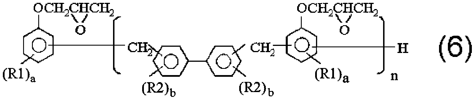

Priority Applications (4)
| Application Number | Priority Date | Filing Date | Title |
|---|---|---|---|
| KR1020077013906A KR101152040B1 (ko) | 2004-11-30 | 2005-11-25 | 에폭시 수지 조성물 및 반도체장치 |
| KR1020117005936A KR101081619B1 (ko) | 2004-11-30 | 2005-11-25 | 에폭시 수지 조성물 및 반도체장치 |
| CN2005800410378A CN101068846B (zh) | 2004-11-30 | 2005-11-25 | 环氧树脂组合物及半导体器件 |
| KR1020117005937A KR101081723B1 (ko) | 2004-11-30 | 2005-11-25 | 에폭시 수지 조성물 및 반도체장치 |
Applications Claiming Priority (10)
| Application Number | Priority Date | Filing Date | Title |
|---|---|---|---|
| JP2004347743A JP2006152185A (ja) | 2004-11-30 | 2004-11-30 | エポキシ樹脂組成物及び半導体装置 |
| JP2004-347743 | 2004-11-30 | ||
| JP2004-368714 | 2004-12-21 | ||
| JP2004368714A JP2006176554A (ja) | 2004-12-21 | 2004-12-21 | エポキシ樹脂組成物及び半導体装置 |
| JP2005002381A JP4736432B2 (ja) | 2005-01-07 | 2005-01-07 | エポキシ樹脂組成物及び半導体装置 |
| JP2005-002381 | 2005-01-07 | ||
| JP2005-039050 | 2005-02-16 | ||
| JP2005039050A JP2006225464A (ja) | 2005-02-16 | 2005-02-16 | エポキシ樹脂組成物及び半導体装置 |
| JP2005-099390 | 2005-03-30 | ||
| JP2005099390A JP4736506B2 (ja) | 2005-03-30 | 2005-03-30 | エポキシ樹脂組成物及び半導体装置 |
Publications (1)
| Publication Number | Publication Date |
|---|---|
| WO2006059542A1 true WO2006059542A1 (ja) | 2006-06-08 |
Family
ID=36564976
Family Applications (1)
| Application Number | Title | Priority Date | Filing Date |
|---|---|---|---|
| PCT/JP2005/021658 Ceased WO2006059542A1 (ja) | 2004-11-30 | 2005-11-25 | エポキシ樹脂組成物及び半導体装置 |
Country Status (7)
| Country | Link |
|---|---|
| US (5) | US20060157872A1 (ja) |
| KR (3) | KR101081723B1 (ja) |
| CN (2) | CN102617981B (ja) |
| MY (3) | MY150607A (ja) |
| SG (4) | SG156623A1 (ja) |
| TW (3) | TWI478969B (ja) |
| WO (1) | WO2006059542A1 (ja) |
Cited By (2)
| Publication number | Priority date | Publication date | Assignee | Title |
|---|---|---|---|---|
| JP2008007692A (ja) * | 2006-06-30 | 2008-01-17 | Sumitomo Bakelite Co Ltd | 封止用エポキシ樹脂組成物及び電子部品装置 |
| JP2012167215A (ja) * | 2011-02-15 | 2012-09-06 | Ube Industries Ltd | 変性ジエン系ゴム及びその製造方法並びにそれを用いたゴム組成物 |
Families Citing this family (19)
| Publication number | Priority date | Publication date | Assignee | Title |
|---|---|---|---|---|
| SG156623A1 (en) * | 2004-11-30 | 2009-11-26 | Sumitomo Bakelite Co | Epoxy resin composition and semiconductor device |
| JP5306592B2 (ja) * | 2006-12-04 | 2013-10-02 | 東レ・ダウコーニング株式会社 | 硬化性エポキシ樹脂組成物、硬化物、およびその用途 |
| JP2009215484A (ja) * | 2008-03-12 | 2009-09-24 | Toshiba Corp | 樹脂組成物及びそれを用いた半導体装置 |
| JP5578168B2 (ja) * | 2009-03-11 | 2014-08-27 | 住友ベークライト株式会社 | 半導体封止用樹脂組成物及び半導体装置 |
| JP5185890B2 (ja) * | 2009-06-17 | 2013-04-17 | 株式会社日立産機システム | 高電圧電気機器用絶縁注型樹脂及びこれを用いた高電圧電気機器 |
| JPWO2011052157A1 (ja) * | 2009-10-26 | 2013-03-14 | 住友ベークライト株式会社 | 半導体封止用樹脂組成物およびこれを用いた半導体装置 |
| JP5874633B2 (ja) * | 2010-05-28 | 2016-03-02 | 住友ベークライト株式会社 | 半導体封止用エポキシ樹脂組成物の製造方法およびこれを用いる半導体装置の製造方法 |
| JP5877163B2 (ja) * | 2010-12-27 | 2016-03-02 | 東レ・ダウコーニング株式会社 | 硬化性エポキシ樹脂組成物 |
| KR101309820B1 (ko) * | 2010-12-29 | 2013-09-23 | 제일모직주식회사 | 반도체 소자 밀봉용 에폭시 수지 조성물 및 이를 이용한 반도체 소자 |
| JP6051630B2 (ja) * | 2011-07-13 | 2016-12-27 | 味の素株式会社 | 半導体パッケージ |
| JP5799694B2 (ja) * | 2011-09-12 | 2015-10-28 | 日立化成株式会社 | 半導体封止用エポキシ樹脂組成物およびそれを用いた半導体装置 |
| JP6181907B2 (ja) * | 2011-11-15 | 2017-08-16 | 互応化学工業株式会社 | カルボキシル基含有樹脂及びソルダーレジスト用樹脂組成物 |
| US9434870B2 (en) | 2012-09-19 | 2016-09-06 | Momentive Performance Materials Inc. | Thermally conductive plastic compositions, extrusion apparatus and methods for making thermally conductive plastics |
| US20140080951A1 (en) * | 2012-09-19 | 2014-03-20 | Chandrashekar Raman | Thermally conductive plastic compositions, extrusion apparatus and methods for making thermally conductive plastics |
| US20160111380A1 (en) * | 2014-10-21 | 2016-04-21 | Georgia Tech Research Corporation | New structure of microelectronic packages with edge protection by coating |
| JP6800227B2 (ja) * | 2015-12-01 | 2020-12-16 | スリーエム イノベイティブ プロパティズ カンパニー | Bステージ化可能な接着剤組成物 |
| JPWO2017099194A1 (ja) * | 2015-12-11 | 2018-09-27 | 日本化薬株式会社 | エポキシ樹脂組成物、プリプレグ、エポキシ樹脂組成物成型体及びその硬化物 |
| JP7102093B2 (ja) * | 2016-09-28 | 2022-07-19 | 味の素株式会社 | 樹脂組成物、樹脂シート、回路基板及び半導体チップパッケージ |
| JP7255411B2 (ja) * | 2019-07-30 | 2023-04-11 | 味の素株式会社 | 樹脂組成物 |
Citations (9)
| Publication number | Priority date | Publication date | Assignee | Title |
|---|---|---|---|---|
| JPH10120873A (ja) * | 1996-10-14 | 1998-05-12 | Sumitomo Bakelite Co Ltd | 半導体用絶縁樹脂ペースト |
| JPH10158365A (ja) * | 1996-12-04 | 1998-06-16 | Sumitomo Bakelite Co Ltd | 液状エポキシ樹脂封止材料 |
| JPH11140274A (ja) * | 1997-11-05 | 1999-05-25 | Sumitomo Bakelite Co Ltd | エポキシ樹脂組成物及び半導体装置 |
| JP2000034393A (ja) * | 1998-05-15 | 2000-02-02 | Shin Etsu Chem Co Ltd | 半導体封止用エポキシ樹脂組成物及び半導体装置 |
| JP2002356538A (ja) * | 2001-03-30 | 2002-12-13 | Toray Ind Inc | 半導体封止用エポキシ樹脂組成物及びそれを用いた半導体装置 |
| JP2003128874A (ja) * | 2001-10-29 | 2003-05-08 | Sumitomo Bakelite Co Ltd | 液状樹脂組成物、半導体装置の製造方法及び半導体装置 |
| JP2004168907A (ja) * | 2002-11-20 | 2004-06-17 | Sumitomo Bakelite Co Ltd | ダイアタッチペースト及び半導体装置 |
| JP2004168922A (ja) * | 2002-11-21 | 2004-06-17 | Sumitomo Bakelite Co Ltd | ダイアタッチペースト及び半導体装置 |
| JP2004292514A (ja) * | 2003-03-25 | 2004-10-21 | Sumitomo Bakelite Co Ltd | エポキシ樹脂組成物及び半導体装置 |
Family Cites Families (11)
| Publication number | Priority date | Publication date | Assignee | Title |
|---|---|---|---|---|
| US4465542A (en) * | 1982-02-19 | 1984-08-14 | Mitsui Petrochemical Industries, Ltd. | Adhesive composition |
| US4578425A (en) * | 1985-02-13 | 1986-03-25 | Schenectady Chemicals, Inc. | Phenolic resins, carboxylic resins and the elastomers containing adhesive |
| JPH11172077A (ja) | 1997-12-11 | 1999-06-29 | Toshiba Chem Corp | 半導体封止用樹脂組成物 |
| JP2000007890A (ja) * | 1998-04-23 | 2000-01-11 | Nitto Denko Corp | 半導体封止用エポキシ樹脂組成物およびその製法ならびに半導体装置 |
| JP2000343393A (ja) * | 1999-05-28 | 2000-12-12 | Nippei Toyama Corp | 円形薄板のエッジ研削装置 |
| KR100878415B1 (ko) * | 2001-09-28 | 2009-01-13 | 스미토모 베이클리트 컴퍼니 리미티드 | 에폭시 수지 조성물 및 반도체 장치 |
| JP4202632B2 (ja) | 2001-09-28 | 2008-12-24 | 株式会社東芝 | 一括封止型半導体パッケージの樹脂封止構造およびその製造装置 |
| JP2004075748A (ja) * | 2002-08-12 | 2004-03-11 | Kyocera Chemical Corp | 難燃性接着剤組成物、フレキシブル銅張板、カバーレイ及び接着フィルム |
| JP2004200034A (ja) | 2002-12-19 | 2004-07-15 | Seiko Epson Corp | 電気光学装置及びその製造方法並びに電子機器 |
| JP2005162826A (ja) * | 2003-12-01 | 2005-06-23 | Kyocera Chemical Corp | 封止用樹脂組成物および樹脂封止型半導体装置 |
| SG156623A1 (en) * | 2004-11-30 | 2009-11-26 | Sumitomo Bakelite Co | Epoxy resin composition and semiconductor device |
-
2005
- 2005-11-25 SG SG200906719-0A patent/SG156623A1/en unknown
- 2005-11-25 SG SG10201406279UA patent/SG10201406279UA/en unknown
- 2005-11-25 CN CN201210063222.9A patent/CN102617981B/zh not_active Expired - Fee Related
- 2005-11-25 SG SG10201406277RA patent/SG10201406277RA/en unknown
- 2005-11-25 SG SG10201406280UA patent/SG10201406280UA/en unknown
- 2005-11-25 CN CN201210063230.3A patent/CN102627832B/zh not_active Expired - Fee Related
- 2005-11-25 WO PCT/JP2005/021658 patent/WO2006059542A1/ja not_active Ceased
- 2005-11-25 KR KR1020117005937A patent/KR101081723B1/ko not_active Expired - Fee Related
- 2005-11-25 KR KR1020077013906A patent/KR101152040B1/ko not_active Expired - Fee Related
- 2005-11-25 KR KR1020117005936A patent/KR101081619B1/ko not_active Expired - Fee Related
- 2005-11-29 MY MYPI20113757 patent/MY150607A/en unknown
- 2005-11-29 MY MYPI20055572 patent/MY150688A/en unknown
- 2005-11-29 US US11/289,265 patent/US20060157872A1/en not_active Abandoned
- 2005-11-29 MY MYPI20113758 patent/MY150584A/en unknown
- 2005-11-30 TW TW101128572A patent/TWI478969B/zh not_active IP Right Cessation
- 2005-11-30 TW TW101128571A patent/TWI527854B/zh not_active IP Right Cessation
- 2005-11-30 TW TW094142028A patent/TWI378968B/zh not_active IP Right Cessation
-
2008
- 2008-11-13 US US12/270,162 patent/US8324326B2/en not_active Expired - Fee Related
-
2012
- 2012-11-02 US US13/667,318 patent/US8921461B2/en not_active Expired - Fee Related
- 2012-11-02 US US13/667,367 patent/US8519067B2/en not_active Expired - Fee Related
- 2012-11-02 US US13/667,344 patent/US8697803B2/en not_active Expired - Fee Related
Patent Citations (9)
| Publication number | Priority date | Publication date | Assignee | Title |
|---|---|---|---|---|
| JPH10120873A (ja) * | 1996-10-14 | 1998-05-12 | Sumitomo Bakelite Co Ltd | 半導体用絶縁樹脂ペースト |
| JPH10158365A (ja) * | 1996-12-04 | 1998-06-16 | Sumitomo Bakelite Co Ltd | 液状エポキシ樹脂封止材料 |
| JPH11140274A (ja) * | 1997-11-05 | 1999-05-25 | Sumitomo Bakelite Co Ltd | エポキシ樹脂組成物及び半導体装置 |
| JP2000034393A (ja) * | 1998-05-15 | 2000-02-02 | Shin Etsu Chem Co Ltd | 半導体封止用エポキシ樹脂組成物及び半導体装置 |
| JP2002356538A (ja) * | 2001-03-30 | 2002-12-13 | Toray Ind Inc | 半導体封止用エポキシ樹脂組成物及びそれを用いた半導体装置 |
| JP2003128874A (ja) * | 2001-10-29 | 2003-05-08 | Sumitomo Bakelite Co Ltd | 液状樹脂組成物、半導体装置の製造方法及び半導体装置 |
| JP2004168907A (ja) * | 2002-11-20 | 2004-06-17 | Sumitomo Bakelite Co Ltd | ダイアタッチペースト及び半導体装置 |
| JP2004168922A (ja) * | 2002-11-21 | 2004-06-17 | Sumitomo Bakelite Co Ltd | ダイアタッチペースト及び半導体装置 |
| JP2004292514A (ja) * | 2003-03-25 | 2004-10-21 | Sumitomo Bakelite Co Ltd | エポキシ樹脂組成物及び半導体装置 |
Cited By (2)
| Publication number | Priority date | Publication date | Assignee | Title |
|---|---|---|---|---|
| JP2008007692A (ja) * | 2006-06-30 | 2008-01-17 | Sumitomo Bakelite Co Ltd | 封止用エポキシ樹脂組成物及び電子部品装置 |
| JP2012167215A (ja) * | 2011-02-15 | 2012-09-06 | Ube Industries Ltd | 変性ジエン系ゴム及びその製造方法並びにそれを用いたゴム組成物 |
Also Published As
| Publication number | Publication date |
|---|---|
| KR101081619B1 (ko) | 2011-11-09 |
| KR20110043762A (ko) | 2011-04-27 |
| CN102617981B (zh) | 2016-12-14 |
| KR20110041577A (ko) | 2011-04-21 |
| TW200626660A (en) | 2006-08-01 |
| US8519067B2 (en) | 2013-08-27 |
| MY150607A (en) | 2014-01-30 |
| SG10201406277RA (en) | 2014-11-27 |
| TW201245307A (en) | 2012-11-16 |
| US8324326B2 (en) | 2012-12-04 |
| SG10201406279UA (en) | 2014-11-27 |
| KR20070100253A (ko) | 2007-10-10 |
| US20060157872A1 (en) | 2006-07-20 |
| US20130134610A1 (en) | 2013-05-30 |
| SG156623A1 (en) | 2009-11-26 |
| US20130113122A1 (en) | 2013-05-09 |
| MY150688A (en) | 2014-02-28 |
| KR101081723B1 (ko) | 2011-11-08 |
| CN102627832A (zh) | 2012-08-08 |
| US20130119564A1 (en) | 2013-05-16 |
| MY150584A (en) | 2014-01-30 |
| TWI527854B (zh) | 2016-04-01 |
| TW201249920A (en) | 2012-12-16 |
| CN102627832B (zh) | 2017-04-26 |
| US8697803B2 (en) | 2014-04-15 |
| TWI378968B (en) | 2012-12-11 |
| KR101152040B1 (ko) | 2012-07-23 |
| CN102617981A (zh) | 2012-08-01 |
| TWI478969B (zh) | 2015-04-01 |
| SG10201406280UA (en) | 2014-11-27 |
| US20090096114A1 (en) | 2009-04-16 |
| US8921461B2 (en) | 2014-12-30 |
Similar Documents
| Publication | Publication Date | Title |
|---|---|---|
| WO2006059542A1 (ja) | エポキシ樹脂組成物及び半導体装置 | |
| JP2013067694A (ja) | 半導体封止用エポキシ樹脂組成物および半導体装置 | |
| JP2006152185A (ja) | エポキシ樹脂組成物及び半導体装置 | |
| JP4622221B2 (ja) | エポキシ樹脂組成物及び半導体装置 | |
| JP4736432B2 (ja) | エポキシ樹脂組成物及び半導体装置 | |
| JP4306329B2 (ja) | エポキシ樹脂組成物及び半導体装置 | |
| JP4496740B2 (ja) | エポキシ樹脂組成物及び半導体装置 | |
| JP5407767B2 (ja) | エポキシ樹脂組成物及び半導体装置 | |
| JP4736506B2 (ja) | エポキシ樹脂組成物及び半導体装置 | |
| JP2004292514A (ja) | エポキシ樹脂組成物及び半導体装置 | |
| JP2006176555A (ja) | エポキシ樹脂組成物及び半導体装置 | |
| JP4172065B2 (ja) | エポキシ樹脂組成物及び電子部品装置 | |
| JP2009256475A (ja) | 半導体封止用エポキシ樹脂組成物およびそれを用いた半導体装置 | |
| JP4736406B2 (ja) | エポキシ樹脂組成物及び半導体装置 | |
| JP2005154717A (ja) | エポキシ樹脂組成物及び半導体装置 | |
| JP2005281584A (ja) | エポキシ樹脂組成物及び半導体装置 | |
| JP5093977B2 (ja) | エリア実装型半導体装置 | |
| JP5055778B2 (ja) | エポキシ樹脂組成物、エポキシ樹脂成形材料及び半導体装置 | |
| JP4543638B2 (ja) | エポキシ樹脂組成物及び半導体装置 | |
| JP5326975B2 (ja) | 半導体封止用エポキシ樹脂組成物、および半導体装置 | |
| JP2006225464A (ja) | エポキシ樹脂組成物及び半導体装置 | |
| JP2007231252A (ja) | 半導体封止用エポキシ樹脂組成物及び該組成物で封止された半導体装置 | |
| JP2006143950A (ja) | エポキシ樹脂組成物及び半導体装置 | |
| JP2006022188A (ja) | エポキシ樹脂組成物及びその製造方法並びに半導体装置 | |
| JP4686935B2 (ja) | 半導体封止用エポキシ樹脂組成物及び半導体装置 |
Legal Events
| Date | Code | Title | Description |
|---|---|---|---|
| AK | Designated states |
Kind code of ref document: A1 Designated state(s): AE AG AL AM AT AU AZ BA BB BG BR BW BY BZ CA CH CN CO CR CU CZ DE DK DM DZ EC EE EG ES FI GB GD GE GH GM HR HU ID IL IN IS KE KG KM KN KP KR KZ LC LK LR LS LT LU LV LY MA MD MG MK MN MW MX MZ NA NG NI NO NZ OM PG PH PL PT RO RU SC SD SE SG SK SL SM SY TJ TM TN TR TT TZ UA UG US UZ VC VN YU ZA ZM ZW |
|
| AL | Designated countries for regional patents |
Kind code of ref document: A1 Designated state(s): BW GH GM KE LS MW MZ NA SD SL SZ TZ UG ZM ZW AM AZ BY KG KZ MD RU TJ TM AT BE BG CH CY CZ DE DK EE ES FI FR GB GR HU IE IS IT LT LU LV MC NL PL PT RO SE SI SK TR BF BJ CF CG CI CM GA GN GQ GW ML MR NE SN TD TG |
|
| 121 | Ep: the epo has been informed by wipo that ep was designated in this application | ||
| WWE | Wipo information: entry into national phase |
Ref document number: 200580041037.8 Country of ref document: CN |
|
| NENP | Non-entry into the national phase |
Ref country code: DE |
|
| WWE | Wipo information: entry into national phase |
Ref document number: 1020077013906 Country of ref document: KR |
|
| 122 | Ep: pct application non-entry in european phase |
Ref document number: 05809565 Country of ref document: EP Kind code of ref document: A1 |
|
| WWE | Wipo information: entry into national phase |
Ref document number: 1020117005937 Country of ref document: KR Ref document number: 1020117005936 Country of ref document: KR Ref document number: KR |