WO2006059532A1 - パターン形成材料、並びにパターン形成装置及びパターン形成方法 - Google Patents
パターン形成材料、並びにパターン形成装置及びパターン形成方法 Download PDFInfo
- Publication number
- WO2006059532A1 WO2006059532A1 PCT/JP2005/021589 JP2005021589W WO2006059532A1 WO 2006059532 A1 WO2006059532 A1 WO 2006059532A1 JP 2005021589 W JP2005021589 W JP 2005021589W WO 2006059532 A1 WO2006059532 A1 WO 2006059532A1
- Authority
- WO
- WIPO (PCT)
- Prior art keywords
- light
- pattern forming
- copolymer
- forming material
- group
- Prior art date
Links
- 239000000463 material Substances 0.000 title claims abstract description 201
- 238000000034 method Methods 0.000 title claims abstract description 114
- 230000007261 regionalization Effects 0.000 title claims abstract description 27
- 229920001577 copolymer Polymers 0.000 claims abstract description 228
- 150000001875 compounds Chemical class 0.000 claims abstract description 101
- 239000011230 binding agent Substances 0.000 claims abstract description 85
- 239000000178 monomer Substances 0.000 claims abstract description 65
- 239000002253 acid Substances 0.000 claims abstract description 47
- 239000003999 initiator Substances 0.000 claims abstract description 24
- 229920001519 homopolymer Polymers 0.000 claims abstract description 8
- PPBRXRYQALVLMV-UHFFFAOYSA-N Styrene Chemical compound C=CC1=CC=CC=C1 PPBRXRYQALVLMV-UHFFFAOYSA-N 0.000 claims description 198
- -1 thio compound Chemical class 0.000 claims description 154
- 238000011161 development Methods 0.000 claims description 35
- 230000018109 developmental process Effects 0.000 claims description 35
- 125000003118 aryl group Chemical group 0.000 claims description 28
- 230000001678 irradiating effect Effects 0.000 claims description 25
- 230000004075 alteration Effects 0.000 claims description 17
- JOYRKODLDBILNP-UHFFFAOYSA-N urethane group Chemical group NC(=O)OCC JOYRKODLDBILNP-UHFFFAOYSA-N 0.000 claims description 13
- 150000003440 styrenes Chemical class 0.000 claims description 10
- 150000008282 halocarbons Chemical class 0.000 claims description 6
- 150000003839 salts Chemical class 0.000 claims description 6
- 150000002923 oximes Chemical class 0.000 claims description 5
- 150000001451 organic peroxides Chemical class 0.000 claims description 3
- 230000009477 glass transition Effects 0.000 abstract description 9
- 239000010410 layer Substances 0.000 description 185
- CERQOIWHTDAKMF-UHFFFAOYSA-N Methacrylic acid Chemical compound CC(=C)C(O)=O CERQOIWHTDAKMF-UHFFFAOYSA-N 0.000 description 139
- 239000000203 mixture Substances 0.000 description 138
- NIXOWILDQLNWCW-UHFFFAOYSA-M Acrylate Chemical compound [O-]C(=O)C=C NIXOWILDQLNWCW-UHFFFAOYSA-M 0.000 description 124
- 239000013307 optical fiber Substances 0.000 description 101
- 238000007334 copolymerization reaction Methods 0.000 description 83
- 230000003287 optical effect Effects 0.000 description 80
- 125000002496 methyl group Chemical group [H]C([H])([H])* 0.000 description 69
- 238000005530 etching Methods 0.000 description 51
- 239000000758 substrate Substances 0.000 description 48
- 239000000243 solution Substances 0.000 description 44
- 230000004907 flux Effects 0.000 description 41
- ISWSIDIOOBJBQZ-UHFFFAOYSA-N phenol group Chemical group C1(=CC=CC=C1)O ISWSIDIOOBJBQZ-UHFFFAOYSA-N 0.000 description 40
- 238000009826 distribution Methods 0.000 description 36
- 239000000835 fiber Substances 0.000 description 36
- 239000010408 film Substances 0.000 description 35
- 238000007747 plating Methods 0.000 description 35
- 239000000126 substance Substances 0.000 description 33
- 239000000049 pigment Substances 0.000 description 29
- LYCAIKOWRPUZTN-UHFFFAOYSA-N Ethylene glycol Chemical compound OCCO LYCAIKOWRPUZTN-UHFFFAOYSA-N 0.000 description 27
- ATUOYWHBWRKTHZ-UHFFFAOYSA-N Propane Chemical compound CCC ATUOYWHBWRKTHZ-UHFFFAOYSA-N 0.000 description 26
- 239000004065 semiconductor Substances 0.000 description 25
- 238000004519 manufacturing process Methods 0.000 description 24
- 238000005253 cladding Methods 0.000 description 23
- 239000011342 resin composition Substances 0.000 description 23
- VVQNEPGJFQJSBK-UHFFFAOYSA-N Methyl methacrylate Chemical compound COC(=O)C(C)=C VVQNEPGJFQJSBK-UHFFFAOYSA-N 0.000 description 21
- HEMHJVSKTPXQMS-UHFFFAOYSA-M Sodium hydroxide Chemical compound [OH-].[Na+] HEMHJVSKTPXQMS-UHFFFAOYSA-M 0.000 description 21
- HRPVXLWXLXDGHG-UHFFFAOYSA-N Acrylamide Chemical compound NC(=O)C=C HRPVXLWXLXDGHG-UHFFFAOYSA-N 0.000 description 19
- RYGMFSIKBFXOCR-UHFFFAOYSA-N Copper Chemical compound [Cu] RYGMFSIKBFXOCR-UHFFFAOYSA-N 0.000 description 19
- 229910052802 copper Inorganic materials 0.000 description 19
- 239000010949 copper Substances 0.000 description 19
- 230000002093 peripheral effect Effects 0.000 description 19
- 230000008569 process Effects 0.000 description 19
- 230000001681 protective effect Effects 0.000 description 19
- 239000007864 aqueous solution Substances 0.000 description 18
- 238000010586 diagram Methods 0.000 description 18
- 238000003384 imaging method Methods 0.000 description 18
- 125000002947 alkylene group Chemical group 0.000 description 17
- 125000004432 carbon atom Chemical group C* 0.000 description 17
- 125000003178 carboxy group Chemical group [H]OC(*)=O 0.000 description 17
- 125000002887 hydroxy group Chemical group [H]O* 0.000 description 16
- LFQSCWFLJHTTHZ-UHFFFAOYSA-N Ethanol Chemical compound CCO LFQSCWFLJHTTHZ-UHFFFAOYSA-N 0.000 description 15
- CDBYLPFSWZWCQE-UHFFFAOYSA-L Sodium Carbonate Chemical compound [Na+].[Na+].[O-]C([O-])=O CDBYLPFSWZWCQE-UHFFFAOYSA-L 0.000 description 15
- RTZKZFJDLAIYFH-UHFFFAOYSA-N Diethyl ether Chemical compound CCOCC RTZKZFJDLAIYFH-UHFFFAOYSA-N 0.000 description 14
- 125000001931 aliphatic group Chemical group 0.000 description 14
- 230000015572 biosynthetic process Effects 0.000 description 14
- 235000019441 ethanol Nutrition 0.000 description 14
- PEDCQBHIVMGVHV-UHFFFAOYSA-N Glycerine Chemical compound OCC(O)CO PEDCQBHIVMGVHV-UHFFFAOYSA-N 0.000 description 13
- 150000002148 esters Chemical class 0.000 description 13
- 239000001294 propane Substances 0.000 description 13
- 125000001424 substituent group Chemical group 0.000 description 13
- 238000011282 treatment Methods 0.000 description 13
- OKKJLVBELUTLKV-UHFFFAOYSA-N Methanol Chemical compound OC OKKJLVBELUTLKV-UHFFFAOYSA-N 0.000 description 12
- KWYUFKZDYYNOTN-UHFFFAOYSA-M Potassium hydroxide Chemical compound [OH-].[K+] KWYUFKZDYYNOTN-UHFFFAOYSA-M 0.000 description 12
- 239000011248 coating agent Substances 0.000 description 12
- 238000000576 coating method Methods 0.000 description 12
- 239000000975 dye Substances 0.000 description 12
- 238000004088 simulation Methods 0.000 description 12
- QZZJTWAHFMBFSX-UHFFFAOYSA-N 2,4-bis(trichloromethyl)-1,3,5-triazine Chemical compound ClC(Cl)(Cl)C1=NC=NC(C(Cl)(Cl)Cl)=N1 QZZJTWAHFMBFSX-UHFFFAOYSA-N 0.000 description 11
- IAYPIBMASNFSPL-UHFFFAOYSA-N Ethylene oxide Chemical class C1CO1 IAYPIBMASNFSPL-UHFFFAOYSA-N 0.000 description 11
- GOOHAUXETOMSMM-UHFFFAOYSA-N Propylene oxide Chemical compound CC1CO1 GOOHAUXETOMSMM-UHFFFAOYSA-N 0.000 description 11
- 125000003866 trichloromethyl group Chemical group ClC(Cl)(Cl)* 0.000 description 11
- ZWEHNKRNPOVVGH-UHFFFAOYSA-N 2-Butanone Chemical compound CCC(C)=O ZWEHNKRNPOVVGH-UHFFFAOYSA-N 0.000 description 10
- 125000000484 butyl group Chemical group [H]C([*])([H])C([H])([H])C([H])([H])C([H])([H])[H] 0.000 description 10
- 238000011156 evaluation Methods 0.000 description 10
- 229920005989 resin Polymers 0.000 description 10
- 239000011347 resin Substances 0.000 description 10
- VZCYOOQTPOCHFL-UHFFFAOYSA-N trans-butenedioic acid Natural products OC(=O)C=CC(O)=O VZCYOOQTPOCHFL-UHFFFAOYSA-N 0.000 description 10
- CSCPPACGZOOCGX-UHFFFAOYSA-N Acetone Chemical compound CC(C)=O CSCPPACGZOOCGX-UHFFFAOYSA-N 0.000 description 9
- UHOVQNZJYSORNB-UHFFFAOYSA-N Benzene Chemical compound C1=CC=CC=C1 UHOVQNZJYSORNB-UHFFFAOYSA-N 0.000 description 9
- ZJCCRDAZUWHFQH-UHFFFAOYSA-N Trimethylolpropane Chemical compound CCC(CO)(CO)CO ZJCCRDAZUWHFQH-UHFFFAOYSA-N 0.000 description 9
- BAPJBEWLBFYGME-UHFFFAOYSA-N acrylic acid methyl ester Natural products COC(=O)C=C BAPJBEWLBFYGME-UHFFFAOYSA-N 0.000 description 9
- 238000012937 correction Methods 0.000 description 9
- 230000000694 effects Effects 0.000 description 9
- 238000010438 heat treatment Methods 0.000 description 9
- 229910052751 metal Inorganic materials 0.000 description 9
- 239000002184 metal Substances 0.000 description 9
- FBPFZTCFMRRESA-FSIIMWSLSA-N D-Glucitol Natural products OC[C@H](O)[C@H](O)[C@@H](O)[C@H](O)CO FBPFZTCFMRRESA-FSIIMWSLSA-N 0.000 description 8
- FBPFZTCFMRRESA-JGWLITMVSA-N D-glucitol Chemical compound OC[C@H](O)[C@@H](O)[C@H](O)[C@H](O)CO FBPFZTCFMRRESA-JGWLITMVSA-N 0.000 description 8
- CERQOIWHTDAKMF-UHFFFAOYSA-M Methacrylate Chemical compound CC(=C)C([O-])=O CERQOIWHTDAKMF-UHFFFAOYSA-M 0.000 description 8
- WYURNTSHIVDZCO-UHFFFAOYSA-N Tetrahydrofuran Chemical compound C1CCOC1 WYURNTSHIVDZCO-UHFFFAOYSA-N 0.000 description 8
- 125000000732 arylene group Chemical group 0.000 description 8
- 125000001797 benzyl group Chemical group [H]C1=C([H])C([H])=C(C([H])=C1[H])C([H])([H])* 0.000 description 8
- 230000000052 comparative effect Effects 0.000 description 8
- WGCNASOHLSPBMP-UHFFFAOYSA-N hydroxyacetaldehyde Natural products OCC=O WGCNASOHLSPBMP-UHFFFAOYSA-N 0.000 description 8
- VNWKTOKETHGBQD-UHFFFAOYSA-N methane Chemical compound C VNWKTOKETHGBQD-UHFFFAOYSA-N 0.000 description 8
- 239000011295 pitch Substances 0.000 description 8
- 229920001223 polyethylene glycol Polymers 0.000 description 8
- BDERNNFJNOPAEC-UHFFFAOYSA-N propan-1-ol Chemical compound CCCO BDERNNFJNOPAEC-UHFFFAOYSA-N 0.000 description 8
- 239000000600 sorbitol Substances 0.000 description 8
- 150000005846 sugar alcohols Polymers 0.000 description 8
- 239000004094 surface-active agent Substances 0.000 description 8
- 125000000391 vinyl group Chemical group [H]C([*])=C([H])[H] 0.000 description 8
- 239000002202 Polyethylene glycol Substances 0.000 description 7
- OFOBLEOULBTSOW-UHFFFAOYSA-N Propanedioic acid Natural products OC(=O)CC(O)=O OFOBLEOULBTSOW-UHFFFAOYSA-N 0.000 description 7
- DNIAPMSPPWPWGF-UHFFFAOYSA-N Propylene glycol Chemical compound CC(O)CO DNIAPMSPPWPWGF-UHFFFAOYSA-N 0.000 description 7
- 230000004888 barrier function Effects 0.000 description 7
- ISAOCJYIOMOJEB-UHFFFAOYSA-N benzoin Chemical compound C=1C=CC=CC=1C(O)C(=O)C1=CC=CC=C1 ISAOCJYIOMOJEB-UHFFFAOYSA-N 0.000 description 7
- 238000009835 boiling Methods 0.000 description 7
- 244000309464 bull Species 0.000 description 7
- 229910052799 carbon Inorganic materials 0.000 description 7
- 239000011521 glass Substances 0.000 description 7
- 150000002430 hydrocarbons Chemical class 0.000 description 7
- NWVVVBRKAWDGAB-UHFFFAOYSA-N hydroquinone methyl ether Natural products COC1=CC=C(O)C=C1 NWVVVBRKAWDGAB-UHFFFAOYSA-N 0.000 description 7
- IQPQWNKOIGAROB-UHFFFAOYSA-N isocyanate group Chemical group [N-]=C=O IQPQWNKOIGAROB-UHFFFAOYSA-N 0.000 description 7
- 239000004973 liquid crystal related substance Substances 0.000 description 7
- 239000011976 maleic acid Substances 0.000 description 7
- LVHBHZANLOWSRM-UHFFFAOYSA-N methylenebutanedioic acid Natural products OC(=O)CC(=C)C(O)=O LVHBHZANLOWSRM-UHFFFAOYSA-N 0.000 description 7
- 229910052757 nitrogen Inorganic materials 0.000 description 7
- 150000002894 organic compounds Chemical class 0.000 description 7
- 238000012545 processing Methods 0.000 description 7
- 230000035945 sensitivity Effects 0.000 description 7
- 229910000029 sodium carbonate Inorganic materials 0.000 description 7
- 239000002904 solvent Substances 0.000 description 7
- 238000003860 storage Methods 0.000 description 7
- LDHQCZJRKDOVOX-UHFFFAOYSA-N trans-crotonic acid Natural products CC=CC(O)=O LDHQCZJRKDOVOX-UHFFFAOYSA-N 0.000 description 7
- DURPTKYDGMDSBL-UHFFFAOYSA-N 1-butoxybutane Chemical class CCCCOCCCC DURPTKYDGMDSBL-UHFFFAOYSA-N 0.000 description 6
- 239000004593 Epoxy Substances 0.000 description 6
- XEKOWRVHYACXOJ-UHFFFAOYSA-N Ethyl acetate Chemical compound CCOC(C)=O XEKOWRVHYACXOJ-UHFFFAOYSA-N 0.000 description 6
- ZMXDDKWLCZADIW-UHFFFAOYSA-N N,N-Dimethylformamide Chemical compound CN(C)C=O ZMXDDKWLCZADIW-UHFFFAOYSA-N 0.000 description 6
- 239000004698 Polyethylene Substances 0.000 description 6
- YXFVVABEGXRONW-UHFFFAOYSA-N Toluene Chemical compound CC1=CC=CC=C1 YXFVVABEGXRONW-UHFFFAOYSA-N 0.000 description 6
- 150000001408 amides Chemical class 0.000 description 6
- 239000002585 base Substances 0.000 description 6
- 230000008878 coupling Effects 0.000 description 6
- 238000010168 coupling process Methods 0.000 description 6
- 238000005859 coupling reaction Methods 0.000 description 6
- MTHSVFCYNBDYFN-UHFFFAOYSA-N diethylene glycol Chemical compound OCCOCCO MTHSVFCYNBDYFN-UHFFFAOYSA-N 0.000 description 6
- PCHJSUWPFVWCPO-UHFFFAOYSA-N gold Chemical compound [Au] PCHJSUWPFVWCPO-UHFFFAOYSA-N 0.000 description 6
- 229910052737 gold Inorganic materials 0.000 description 6
- 239000010931 gold Substances 0.000 description 6
- 150000002366 halogen compounds Chemical class 0.000 description 6
- 238000005192 partition Methods 0.000 description 6
- 229940059574 pentaerithrityl Drugs 0.000 description 6
- WXZMFSXDPGVJKK-UHFFFAOYSA-N pentaerythritol Chemical compound OCC(CO)(CO)CO WXZMFSXDPGVJKK-UHFFFAOYSA-N 0.000 description 6
- 229920000573 polyethylene Polymers 0.000 description 6
- 229920000139 polyethylene terephthalate Polymers 0.000 description 6
- 239000005020 polyethylene terephthalate Substances 0.000 description 6
- 125000006850 spacer group Chemical group 0.000 description 6
- 238000012719 thermal polymerization Methods 0.000 description 6
- 229920002554 vinyl polymer Polymers 0.000 description 6
- GOLORTLGFDVFDW-UHFFFAOYSA-N 3-(1h-benzimidazol-2-yl)-7-(diethylamino)chromen-2-one Chemical compound C1=CC=C2NC(C3=CC4=CC=C(C=C4OC3=O)N(CC)CC)=NC2=C1 GOLORTLGFDVFDW-UHFFFAOYSA-N 0.000 description 5
- SOGAXMICEFXMKE-UHFFFAOYSA-N Butylmethacrylate Chemical compound CCCCOC(=O)C(C)=C SOGAXMICEFXMKE-UHFFFAOYSA-N 0.000 description 5
- KFZMGEQAYNKOFK-UHFFFAOYSA-N Isopropanol Chemical compound CC(C)O KFZMGEQAYNKOFK-UHFFFAOYSA-N 0.000 description 5
- LRHPLDYGYMQRHN-UHFFFAOYSA-N N-Butanol Chemical class CCCCO LRHPLDYGYMQRHN-UHFFFAOYSA-N 0.000 description 5
- 239000004743 Polypropylene Substances 0.000 description 5
- 239000007983 Tris buffer Substances 0.000 description 5
- 239000002318 adhesion promoter Substances 0.000 description 5
- 150000001298 alcohols Chemical class 0.000 description 5
- 238000003491 array Methods 0.000 description 5
- ZYGHJZDHTFUPRJ-UHFFFAOYSA-N benzo-alpha-pyrone Natural products C1=CC=C2OC(=O)C=CC2=C1 ZYGHJZDHTFUPRJ-UHFFFAOYSA-N 0.000 description 5
- 239000012965 benzophenone Substances 0.000 description 5
- 230000008033 biological extinction Effects 0.000 description 5
- IISBACLAFKSPIT-UHFFFAOYSA-N bisphenol A Chemical compound C=1C=C(O)C=CC=1C(C)(C)C1=CC=C(O)C=C1 IISBACLAFKSPIT-UHFFFAOYSA-N 0.000 description 5
- 239000003086 colorant Substances 0.000 description 5
- LDHQCZJRKDOVOX-NSCUHMNNSA-N crotonic acid Chemical compound C\C=C\C(O)=O LDHQCZJRKDOVOX-NSCUHMNNSA-N 0.000 description 5
- 125000000113 cyclohexyl group Chemical group [H]C1([H])C([H])([H])C([H])([H])C([H])(*)C([H])([H])C1([H])[H] 0.000 description 5
- 125000005442 diisocyanate group Chemical group 0.000 description 5
- 125000000118 dimethyl group Chemical group [H]C([H])([H])* 0.000 description 5
- 238000001035 drying Methods 0.000 description 5
- 125000001301 ethoxy group Chemical group [H]C([H])([H])C([H])([H])O* 0.000 description 5
- 230000007274 generation of a signal involved in cell-cell signaling Effects 0.000 description 5
- 235000011187 glycerol Nutrition 0.000 description 5
- 125000005843 halogen group Chemical group 0.000 description 5
- 125000004435 hydrogen atom Chemical group [H]* 0.000 description 5
- 125000001841 imino group Chemical group [H]N=* 0.000 description 5
- 239000003112 inhibitor Substances 0.000 description 5
- 238000010030 laminating Methods 0.000 description 5
- PXHVJJICTQNCMI-UHFFFAOYSA-N nickel Substances [Ni] PXHVJJICTQNCMI-UHFFFAOYSA-N 0.000 description 5
- 239000004014 plasticizer Substances 0.000 description 5
- 238000006116 polymerization reaction Methods 0.000 description 5
- 229920001155 polypropylene Polymers 0.000 description 5
- 229920001451 polypropylene glycol Polymers 0.000 description 5
- 125000002924 primary amino group Chemical group [H]N([H])* 0.000 description 5
- 239000000047 product Substances 0.000 description 5
- 238000005507 spraying Methods 0.000 description 5
- 229920006163 vinyl copolymer Polymers 0.000 description 5
- XLYOFNOQVPJJNP-UHFFFAOYSA-N water Substances O XLYOFNOQVPJJNP-UHFFFAOYSA-N 0.000 description 5
- JYEUMXHLPRZUAT-UHFFFAOYSA-N 1,2,3-triazine Chemical group C1=CN=NN=C1 JYEUMXHLPRZUAT-UHFFFAOYSA-N 0.000 description 4
- ARXKVVRQIIOZGF-UHFFFAOYSA-N 1,2,4-butanetriol Chemical compound OCCC(O)CO ARXKVVRQIIOZGF-UHFFFAOYSA-N 0.000 description 4
- ARXJGSRGQADJSQ-UHFFFAOYSA-N 1-methoxypropan-2-ol Chemical compound COCC(C)O ARXJGSRGQADJSQ-UHFFFAOYSA-N 0.000 description 4
- NIXOWILDQLNWCW-UHFFFAOYSA-N 2-Propenoic acid Natural products OC(=O)C=C NIXOWILDQLNWCW-UHFFFAOYSA-N 0.000 description 4
- TXBCBTDQIULDIA-UHFFFAOYSA-N 2-[[3-hydroxy-2,2-bis(hydroxymethyl)propoxy]methyl]-2-(hydroxymethyl)propane-1,3-diol Chemical compound OCC(CO)(CO)COCC(CO)(CO)CO TXBCBTDQIULDIA-UHFFFAOYSA-N 0.000 description 4
- JVVRCYWZTJLJSG-UHFFFAOYSA-N 4-dimethylaminophenol Chemical compound CN(C)C1=CC=C(O)C=C1 JVVRCYWZTJLJSG-UHFFFAOYSA-N 0.000 description 4
- VZCYOOQTPOCHFL-OWOJBTEDSA-N Fumaric acid Chemical compound OC(=O)\C=C\C(O)=O VZCYOOQTPOCHFL-OWOJBTEDSA-N 0.000 description 4
- MHAJPDPJQMAIIY-UHFFFAOYSA-N Hydrogen peroxide Chemical compound OO MHAJPDPJQMAIIY-UHFFFAOYSA-N 0.000 description 4
- QIGBRXMKCJKVMJ-UHFFFAOYSA-N Hydroquinone Chemical compound OC1=CC=C(O)C=C1 QIGBRXMKCJKVMJ-UHFFFAOYSA-N 0.000 description 4
- XEEYBQQBJWHFJM-UHFFFAOYSA-N Iron Chemical compound [Fe] XEEYBQQBJWHFJM-UHFFFAOYSA-N 0.000 description 4
- 244000028419 Styrax benzoin Species 0.000 description 4
- 235000000126 Styrax benzoin Nutrition 0.000 description 4
- 235000008411 Sumatra benzointree Nutrition 0.000 description 4
- 125000002777 acetyl group Chemical group [H]C([H])([H])C(*)=O 0.000 description 4
- 239000000654 additive Substances 0.000 description 4
- 125000003545 alkoxy group Chemical group 0.000 description 4
- 125000000217 alkyl group Chemical group 0.000 description 4
- 229960002130 benzoin Drugs 0.000 description 4
- RWCCWEUUXYIKHB-UHFFFAOYSA-N benzophenone Chemical compound C=1C=CC=CC=1C(=O)C1=CC=CC=C1 RWCCWEUUXYIKHB-UHFFFAOYSA-N 0.000 description 4
- BTANRVKWQNVYAZ-UHFFFAOYSA-N butan-2-ol Chemical compound CCC(C)O BTANRVKWQNVYAZ-UHFFFAOYSA-N 0.000 description 4
- CDQSJQSWAWPGKG-UHFFFAOYSA-N butane-1,1-diol Chemical compound CCCC(O)O CDQSJQSWAWPGKG-UHFFFAOYSA-N 0.000 description 4
- 150000001721 carbon Chemical group 0.000 description 4
- 150000001732 carboxylic acid derivatives Chemical class 0.000 description 4
- ORTQZVOHEJQUHG-UHFFFAOYSA-L copper(II) chloride Chemical compound Cl[Cu]Cl ORTQZVOHEJQUHG-UHFFFAOYSA-L 0.000 description 4
- 235000001671 coumarin Nutrition 0.000 description 4
- 230000007423 decrease Effects 0.000 description 4
- 230000007547 defect Effects 0.000 description 4
- 238000001514 detection method Methods 0.000 description 4
- DOIRQSBPFJWKBE-UHFFFAOYSA-N dibutyl phthalate Chemical compound CCCCOC(=O)C1=CC=CC=C1C(=O)OCCCC DOIRQSBPFJWKBE-UHFFFAOYSA-N 0.000 description 4
- 239000003822 epoxy resin Substances 0.000 description 4
- 150000002170 ethers Chemical class 0.000 description 4
- 229940052303 ethers for general anesthesia Drugs 0.000 description 4
- 125000000524 functional group Chemical group 0.000 description 4
- 230000004927 fusion Effects 0.000 description 4
- 235000019382 gum benzoic Nutrition 0.000 description 4
- ZSIAUFGUXNUGDI-UHFFFAOYSA-N hexan-1-ol Chemical compound CCCCCCO ZSIAUFGUXNUGDI-UHFFFAOYSA-N 0.000 description 4
- ZFSLODLOARCGLH-UHFFFAOYSA-N isocyanuric acid Chemical compound OC1=NC(O)=NC(O)=N1 ZFSLODLOARCGLH-UHFFFAOYSA-N 0.000 description 4
- VZCYOOQTPOCHFL-UPHRSURJSA-N maleic acid Chemical compound OC(=O)\C=C/C(O)=O VZCYOOQTPOCHFL-UPHRSURJSA-N 0.000 description 4
- 238000005259 measurement Methods 0.000 description 4
- 125000005395 methacrylic acid group Chemical group 0.000 description 4
- 125000000956 methoxy group Chemical group [H]C([H])([H])O* 0.000 description 4
- CQRYARSYNCAZFO-UHFFFAOYSA-N o-hydroxybenzyl alcohol Natural products OCC1=CC=CC=C1O CQRYARSYNCAZFO-UHFFFAOYSA-N 0.000 description 4
- 239000003960 organic solvent Substances 0.000 description 4
- 125000004430 oxygen atom Chemical group O* 0.000 description 4
- BVJSUAQZOZWCKN-UHFFFAOYSA-N p-hydroxybenzyl alcohol Chemical compound OCC1=CC=C(O)C=C1 BVJSUAQZOZWCKN-UHFFFAOYSA-N 0.000 description 4
- 229920000647 polyepoxide Polymers 0.000 description 4
- 229920000642 polymer Polymers 0.000 description 4
- BWHMMNNQKKPAPP-UHFFFAOYSA-L potassium carbonate Chemical compound [K+].[K+].[O-]C([O-])=O BWHMMNNQKKPAPP-UHFFFAOYSA-L 0.000 description 4
- WQGWDDDVZFFDIG-UHFFFAOYSA-N pyrogallol Chemical compound OC1=CC=CC(O)=C1O WQGWDDDVZFFDIG-UHFFFAOYSA-N 0.000 description 4
- 150000003254 radicals Chemical class 0.000 description 4
- 125000000467 secondary amino group Chemical group [H]N([*:1])[*:2] 0.000 description 4
- 229910000679 solder Inorganic materials 0.000 description 4
- 229910052717 sulfur Inorganic materials 0.000 description 4
- HJUGFYREWKUQJT-UHFFFAOYSA-N tetrabromomethane Chemical compound BrC(Br)(Br)Br HJUGFYREWKUQJT-UHFFFAOYSA-N 0.000 description 4
- YLQBMQCUIZJEEH-UHFFFAOYSA-N tetrahydrofuran Natural products C=1C=COC=1 YLQBMQCUIZJEEH-UHFFFAOYSA-N 0.000 description 4
- UBOXGVDOUJQMTN-UHFFFAOYSA-N 1,1,2-trichloroethane Chemical compound ClCC(Cl)Cl UBOXGVDOUJQMTN-UHFFFAOYSA-N 0.000 description 3
- JAHNSTQSQJOJLO-UHFFFAOYSA-N 2-(3-fluorophenyl)-1h-imidazole Chemical compound FC1=CC=CC(C=2NC=CN=2)=C1 JAHNSTQSQJOJLO-UHFFFAOYSA-N 0.000 description 3
- HSDVRWZKEDRBAG-UHFFFAOYSA-N 2-[1-(oxiran-2-ylmethoxy)hexoxymethyl]oxirane Chemical compound C1OC1COC(CCCCC)OCC1CO1 HSDVRWZKEDRBAG-UHFFFAOYSA-N 0.000 description 3
- SEFYJVFBMNOLBK-UHFFFAOYSA-N 2-[2-[2-(oxiran-2-ylmethoxy)ethoxy]ethoxymethyl]oxirane Chemical compound C1OC1COCCOCCOCC1CO1 SEFYJVFBMNOLBK-UHFFFAOYSA-N 0.000 description 3
- PLDLPVSQYMQDBL-UHFFFAOYSA-N 2-[[3-(oxiran-2-ylmethoxy)-2,2-bis(oxiran-2-ylmethoxymethyl)propoxy]methyl]oxirane Chemical compound C1OC1COCC(COCC1OC1)(COCC1OC1)COCC1CO1 PLDLPVSQYMQDBL-UHFFFAOYSA-N 0.000 description 3
- ZCYVEMRRCGMTRW-UHFFFAOYSA-N 7553-56-2 Chemical group [I] ZCYVEMRRCGMTRW-UHFFFAOYSA-N 0.000 description 3
- WEVYAHXRMPXWCK-UHFFFAOYSA-N Acetonitrile Chemical compound CC#N WEVYAHXRMPXWCK-UHFFFAOYSA-N 0.000 description 3
- OKTJSMMVPCPJKN-UHFFFAOYSA-N Carbon Chemical compound [C] OKTJSMMVPCPJKN-UHFFFAOYSA-N 0.000 description 3
- YMWUJEATGCHHMB-UHFFFAOYSA-N Dichloromethane Chemical compound ClCCl YMWUJEATGCHHMB-UHFFFAOYSA-N 0.000 description 3
- WMFOQBRAJBCJND-UHFFFAOYSA-M Lithium hydroxide Chemical compound [Li+].[OH-] WMFOQBRAJBCJND-UHFFFAOYSA-M 0.000 description 3
- JLTDJTHDQAWBAV-UHFFFAOYSA-N N,N-dimethylaniline Chemical compound CN(C)C1=CC=CC=C1 JLTDJTHDQAWBAV-UHFFFAOYSA-N 0.000 description 3
- MUBZPKHOEPUJKR-UHFFFAOYSA-N Oxalic acid Chemical compound OC(=O)C(O)=O MUBZPKHOEPUJKR-UHFFFAOYSA-N 0.000 description 3
- NBIIXXVUZAFLBC-UHFFFAOYSA-N Phosphoric acid Chemical group OP(O)(O)=O NBIIXXVUZAFLBC-UHFFFAOYSA-N 0.000 description 3
- OAICVXFJPJFONN-UHFFFAOYSA-N Phosphorus Chemical compound [P] OAICVXFJPJFONN-UHFFFAOYSA-N 0.000 description 3
- QAOWNCQODCNURD-UHFFFAOYSA-L Sulfate Chemical compound [O-]S([O-])(=O)=O QAOWNCQODCNURD-UHFFFAOYSA-L 0.000 description 3
- DZCVLTAQZZDCMH-UHFFFAOYSA-N [1-(oxiran-2-ylmethoxymethyl)cyclohexyl]methanol Chemical compound C1OC1COCC1(CO)CCCCC1 DZCVLTAQZZDCMH-UHFFFAOYSA-N 0.000 description 3
- 230000002378 acidificating effect Effects 0.000 description 3
- 238000007259 addition reaction Methods 0.000 description 3
- 150000001412 amines Chemical class 0.000 description 3
- 150000004056 anthraquinones Chemical class 0.000 description 3
- 125000004104 aryloxy group Chemical group 0.000 description 3
- WERYXYBDKMZEQL-UHFFFAOYSA-N butane-1,4-diol Chemical compound OCCCCO WERYXYBDKMZEQL-UHFFFAOYSA-N 0.000 description 3
- 238000004364 calculation method Methods 0.000 description 3
- 239000003795 chemical substances by application Substances 0.000 description 3
- 238000004040 coloring Methods 0.000 description 3
- 150000004775 coumarins Chemical class 0.000 description 3
- 239000013078 crystal Substances 0.000 description 3
- 125000004122 cyclic group Chemical group 0.000 description 3
- IOJUPLGTWVMSFF-UHFFFAOYSA-N cyclobenzothiazole Natural products C1=CC=C2SC=NC2=C1 IOJUPLGTWVMSFF-UHFFFAOYSA-N 0.000 description 3
- OIWOHHBRDFKZNC-UHFFFAOYSA-N cyclohexyl 2-methylprop-2-enoate Chemical compound CC(=C)C(=O)OC1CCCCC1 OIWOHHBRDFKZNC-UHFFFAOYSA-N 0.000 description 3
- SZXQTJUDPRGNJN-UHFFFAOYSA-N dipropylene glycol Chemical compound OCCCOCCCO SZXQTJUDPRGNJN-UHFFFAOYSA-N 0.000 description 3
- 239000000428 dust Substances 0.000 description 3
- YQGOJNYOYNNSMM-UHFFFAOYSA-N eosin Chemical compound [Na+].OC(=O)C1=CC=CC=C1C1=C2C=C(Br)C(=O)C(Br)=C2OC2=C(Br)C(O)=C(Br)C=C21 YQGOJNYOYNNSMM-UHFFFAOYSA-N 0.000 description 3
- 125000004185 ester group Chemical group 0.000 description 3
- 229910052731 fluorine Inorganic materials 0.000 description 3
- 239000001530 fumaric acid Substances 0.000 description 3
- 230000006870 function Effects 0.000 description 3
- 238000005286 illumination Methods 0.000 description 3
- 238000009434 installation Methods 0.000 description 3
- 239000012948 isocyanate Substances 0.000 description 3
- 150000002576 ketones Chemical class 0.000 description 3
- 239000007788 liquid Substances 0.000 description 3
- FDZZZRQASAIRJF-UHFFFAOYSA-M malachite green Chemical compound [Cl-].C1=CC(N(C)C)=CC=C1C(C=1C=CC=CC=1)=C1C=CC(=[N+](C)C)C=C1 FDZZZRQASAIRJF-UHFFFAOYSA-M 0.000 description 3
- 229940107698 malachite green Drugs 0.000 description 3
- 239000011159 matrix material Substances 0.000 description 3
- 125000005641 methacryl group Chemical group 0.000 description 3
- 125000001570 methylene group Chemical group [H]C([H])([*:1])[*:2] 0.000 description 3
- QWVGKYWNOKOFNN-UHFFFAOYSA-N o-methyl phenol Natural products CC1=CC=CC=C1O QWVGKYWNOKOFNN-UHFFFAOYSA-N 0.000 description 3
- 239000005304 optical glass Substances 0.000 description 3
- 125000000962 organic group Chemical group 0.000 description 3
- 150000002896 organic halogen compounds Chemical class 0.000 description 3
- 230000010355 oscillation Effects 0.000 description 3
- 239000000123 paper Substances 0.000 description 3
- 239000002245 particle Substances 0.000 description 3
- 125000000951 phenoxy group Chemical group [H]C1=C([H])C([H])=C(O*)C([H])=C1[H] 0.000 description 3
- 229910052698 phosphorus Inorganic materials 0.000 description 3
- 239000011574 phosphorus Substances 0.000 description 3
- XNGIFLGASWRNHJ-UHFFFAOYSA-L phthalate(2-) Chemical compound [O-]C(=O)C1=CC=CC=C1C([O-])=O XNGIFLGASWRNHJ-UHFFFAOYSA-L 0.000 description 3
- 125000004805 propylene group Chemical group [H]C([H])([H])C([H])([*:1])C([H])([H])[*:2] 0.000 description 3
- 230000009467 reduction Effects 0.000 description 3
- 230000001235 sensitizing effect Effects 0.000 description 3
- 239000007921 spray Substances 0.000 description 3
- 229920003002 synthetic resin Polymers 0.000 description 3
- 239000000057 synthetic resin Substances 0.000 description 3
- RMVRSNDYEFQCLF-UHFFFAOYSA-N thiophenol Chemical compound SC1=CC=CC=C1 RMVRSNDYEFQCLF-UHFFFAOYSA-N 0.000 description 3
- 238000012546 transfer Methods 0.000 description 3
- 238000002834 transmittance Methods 0.000 description 3
- ZIBGPFATKBEMQZ-UHFFFAOYSA-N triethylene glycol Chemical compound OCCOCCOCCO ZIBGPFATKBEMQZ-UHFFFAOYSA-N 0.000 description 3
- XSQUKJJJFZCRTK-UHFFFAOYSA-N urea group Chemical group NC(=O)N XSQUKJJJFZCRTK-UHFFFAOYSA-N 0.000 description 3
- 239000008096 xylene Substances 0.000 description 3
- DNIAPMSPPWPWGF-VKHMYHEASA-N (+)-propylene glycol Chemical compound C[C@H](O)CO DNIAPMSPPWPWGF-VKHMYHEASA-N 0.000 description 2
- HJIAMFHSAAEUKR-UHFFFAOYSA-N (2-hydroxyphenyl)-phenylmethanone Chemical compound OC1=CC=CC=C1C(=O)C1=CC=CC=C1 HJIAMFHSAAEUKR-UHFFFAOYSA-N 0.000 description 2
- PVPBBTJXIKFICP-UHFFFAOYSA-N (7-aminophenothiazin-3-ylidene)azanium;chloride Chemical compound [Cl-].C1=CC(=[NH2+])C=C2SC3=CC(N)=CC=C3N=C21 PVPBBTJXIKFICP-UHFFFAOYSA-N 0.000 description 2
- DJWVKJAGMVZYFP-UHFFFAOYSA-N 1,1,3,3-tetrachloropropan-2-one Chemical compound ClC(Cl)C(=O)C(Cl)Cl DJWVKJAGMVZYFP-UHFFFAOYSA-N 0.000 description 2
- FKASFBLJDCHBNZ-UHFFFAOYSA-N 1,3,4-oxadiazole Chemical compound C1=NN=CO1 FKASFBLJDCHBNZ-UHFFFAOYSA-N 0.000 description 2
- JIHQDMXYYFUGFV-UHFFFAOYSA-N 1,3,5-triazine Chemical compound C1=NC=NC=N1 JIHQDMXYYFUGFV-UHFFFAOYSA-N 0.000 description 2
- YXIWHUQXZSMYRE-UHFFFAOYSA-N 1,3-benzothiazole-2-thiol Chemical compound C1=CC=C2SC(S)=NC2=C1 YXIWHUQXZSMYRE-UHFFFAOYSA-N 0.000 description 2
- YHMYGUUIMTVXNW-UHFFFAOYSA-N 1,3-dihydrobenzimidazole-2-thione Chemical compound C1=CC=C2NC(S)=NC2=C1 YHMYGUUIMTVXNW-UHFFFAOYSA-N 0.000 description 2
- YPFDHNVEDLHUCE-UHFFFAOYSA-N 1,3-propanediol Substances OCCCO YPFDHNVEDLHUCE-UHFFFAOYSA-N 0.000 description 2
- KJCVRFUGPWSIIH-UHFFFAOYSA-N 1-naphthol Chemical compound C1=CC=C2C(O)=CC=CC2=C1 KJCVRFUGPWSIIH-UHFFFAOYSA-N 0.000 description 2
- RUFPHBVGCFYCNW-UHFFFAOYSA-N 1-naphthylamine Chemical compound C1=CC=C2C(N)=CC=CC2=C1 RUFPHBVGCFYCNW-UHFFFAOYSA-N 0.000 description 2
- WJFKNYWRSNBZNX-UHFFFAOYSA-N 10H-phenothiazine Chemical compound C1=CC=C2NC3=CC=CC=C3SC2=C1 WJFKNYWRSNBZNX-UHFFFAOYSA-N 0.000 description 2
- ORCCSQMJUGMAQU-UHFFFAOYSA-N 2,2,2-tribromoacetamide Chemical compound NC(=O)C(Br)(Br)Br ORCCSQMJUGMAQU-UHFFFAOYSA-N 0.000 description 2
- XHAXVDWUMCHTCY-UHFFFAOYSA-N 2,2,2-trichloroethyl acetate Chemical compound CC(=O)OCC(Cl)(Cl)Cl XHAXVDWUMCHTCY-UHFFFAOYSA-N 0.000 description 2
- DXUMYHZTYVPBEZ-UHFFFAOYSA-N 2,4,6-tris(trichloromethyl)-1,3,5-triazine Chemical compound ClC(Cl)(Cl)C1=NC(C(Cl)(Cl)Cl)=NC(C(Cl)(Cl)Cl)=N1 DXUMYHZTYVPBEZ-UHFFFAOYSA-N 0.000 description 2
- SSIZLKDLDKIHEV-UHFFFAOYSA-N 2,6-dibromophenol Chemical compound OC1=C(Br)C=CC=C1Br SSIZLKDLDKIHEV-UHFFFAOYSA-N 0.000 description 2
- FPZWZCWUIYYYBU-UHFFFAOYSA-N 2-(2-ethoxyethoxy)ethyl acetate Chemical group CCOCCOCCOC(C)=O FPZWZCWUIYYYBU-UHFFFAOYSA-N 0.000 description 2
- SMZOUWXMTYCWNB-UHFFFAOYSA-N 2-(2-methoxy-5-methylphenyl)ethanamine Chemical compound COC1=CC=C(C)C=C1CCN SMZOUWXMTYCWNB-UHFFFAOYSA-N 0.000 description 2
- HZAXFHJVJLSVMW-UHFFFAOYSA-N 2-Aminoethan-1-ol Chemical compound NCCO HZAXFHJVJLSVMW-UHFFFAOYSA-N 0.000 description 2
- XNWFRZJHXBZDAG-UHFFFAOYSA-N 2-METHOXYETHANOL Chemical compound COCCO XNWFRZJHXBZDAG-UHFFFAOYSA-N 0.000 description 2
- SYEWHONLFGZGLK-UHFFFAOYSA-N 2-[1,3-bis(oxiran-2-ylmethoxy)propan-2-yloxymethyl]oxirane Chemical compound C1OC1COCC(OCC1OC1)COCC1CO1 SYEWHONLFGZGLK-UHFFFAOYSA-N 0.000 description 2
- RQZUWSJHFBOFPI-UHFFFAOYSA-N 2-[1-[1-(oxiran-2-ylmethoxy)propan-2-yloxy]propan-2-yloxymethyl]oxirane Chemical compound C1OC1COC(C)COC(C)COCC1CO1 RQZUWSJHFBOFPI-UHFFFAOYSA-N 0.000 description 2
- LCZVSXRMYJUNFX-UHFFFAOYSA-N 2-[2-(2-hydroxypropoxy)propoxy]propan-1-ol Chemical compound CC(O)COC(C)COC(C)CO LCZVSXRMYJUNFX-UHFFFAOYSA-N 0.000 description 2
- YIWUKEYIRIRTPP-UHFFFAOYSA-N 2-ethylhexan-1-ol Chemical compound CCCCC(CC)CO YIWUKEYIRIRTPP-UHFFFAOYSA-N 0.000 description 2
- 125000000954 2-hydroxyethyl group Chemical group [H]C([*])([H])C([H])([H])O[H] 0.000 description 2
- FLFWJIBUZQARMD-UHFFFAOYSA-N 2-mercapto-1,3-benzoxazole Chemical compound C1=CC=C2OC(S)=NC2=C1 FLFWJIBUZQARMD-UHFFFAOYSA-N 0.000 description 2
- 125000004200 2-methoxyethyl group Chemical group [H]C([H])([H])OC([H])([H])C([H])([H])* 0.000 description 2
- JWAZRIHNYRIHIV-UHFFFAOYSA-N 2-naphthol Chemical compound C1=CC=CC2=CC(O)=CC=C21 JWAZRIHNYRIHIV-UHFFFAOYSA-N 0.000 description 2
- XLLXMBCBJGATSP-UHFFFAOYSA-N 2-phenylethenol Chemical compound OC=CC1=CC=CC=C1 XLLXMBCBJGATSP-UHFFFAOYSA-N 0.000 description 2
- KKAJSJJFBSOMGS-UHFFFAOYSA-N 3,6-diamino-10-methylacridinium chloride Chemical compound [Cl-].C1=C(N)C=C2[N+](C)=C(C=C(N)C=C3)C3=CC2=C1 KKAJSJJFBSOMGS-UHFFFAOYSA-N 0.000 description 2
- HYORIVUCOQKMOC-UHFFFAOYSA-N 3-benzoyl-7-methoxychromen-2-one Chemical compound O=C1OC2=CC(OC)=CC=C2C=C1C(=O)C1=CC=CC=C1 HYORIVUCOQKMOC-UHFFFAOYSA-N 0.000 description 2
- ASHGTJPOSUFTGB-UHFFFAOYSA-N 3-methoxyphenol Chemical compound COC1=CC=CC(O)=C1 ASHGTJPOSUFTGB-UHFFFAOYSA-N 0.000 description 2
- CCTFMNIEFHGTDU-UHFFFAOYSA-N 3-methoxypropyl acetate Chemical compound COCCCOC(C)=O CCTFMNIEFHGTDU-UHFFFAOYSA-N 0.000 description 2
- MECNWXGGNCJFQJ-UHFFFAOYSA-N 3-piperidin-1-ylpropane-1,2-diol Chemical compound OCC(O)CN1CCCCC1 MECNWXGGNCJFQJ-UHFFFAOYSA-N 0.000 description 2
- IICCLYANAQEHCI-UHFFFAOYSA-N 4,5,6,7-tetrachloro-3',6'-dihydroxy-2',4',5',7'-tetraiodospiro[2-benzofuran-3,9'-xanthene]-1-one Chemical compound O1C(=O)C(C(=C(Cl)C(Cl)=C2Cl)Cl)=C2C21C1=CC(I)=C(O)C(I)=C1OC1=C(I)C(O)=C(I)C=C21 IICCLYANAQEHCI-UHFFFAOYSA-N 0.000 description 2
- BGNGWHSBYQYVRX-UHFFFAOYSA-N 4-(dimethylamino)benzaldehyde Chemical compound CN(C)C1=CC=C(C=O)C=C1 BGNGWHSBYQYVRX-UHFFFAOYSA-N 0.000 description 2
- 229960000549 4-dimethylaminophenol Drugs 0.000 description 2
- QZSNQRPYUPGABZ-UHFFFAOYSA-N 5,7-dipropoxychromen-2-one Chemical compound C1=CC(=O)OC2=CC(OCCC)=CC(OCCC)=C21 QZSNQRPYUPGABZ-UHFFFAOYSA-N 0.000 description 2
- HJCUTNIGJHJGCF-UHFFFAOYSA-N 9,10-dihydroacridine Chemical compound C1=CC=C2CC3=CC=CC=C3NC2=C1 HJCUTNIGJHJGCF-UHFFFAOYSA-N 0.000 description 2
- LRFVTYWOQMYALW-UHFFFAOYSA-N 9H-xanthine Chemical compound O=C1NC(=O)NC2=C1NC=N2 LRFVTYWOQMYALW-UHFFFAOYSA-N 0.000 description 2
- 239000004342 Benzoyl peroxide Substances 0.000 description 2
- 229930185605 Bisphenol Natural products 0.000 description 2
- LCFVJGUPQDGYKZ-UHFFFAOYSA-N Bisphenol A diglycidyl ether Chemical compound C=1C=C(OCC2OC2)C=CC=1C(C)(C)C(C=C1)=CC=C1OCC1CO1 LCFVJGUPQDGYKZ-UHFFFAOYSA-N 0.000 description 2
- WKBOTKDWSSQWDR-UHFFFAOYSA-N Bromine atom Chemical group [Br] WKBOTKDWSSQWDR-UHFFFAOYSA-N 0.000 description 2
- DKPFZGUDAPQIHT-UHFFFAOYSA-N Butyl acetate Natural products CCCCOC(C)=O DKPFZGUDAPQIHT-UHFFFAOYSA-N 0.000 description 2
- IRIAEXORFWYRCZ-UHFFFAOYSA-N Butylbenzyl phthalate Chemical compound CCCCOC(=O)C1=CC=CC=C1C(=O)OCC1=CC=CC=C1 IRIAEXORFWYRCZ-UHFFFAOYSA-N 0.000 description 2
- JUQPZRLQQYSMEQ-UHFFFAOYSA-N CI Basic red 9 Chemical compound [Cl-].C1=CC(N)=CC=C1C(C=1C=CC(N)=CC=1)=C1C=CC(=[NH2+])C=C1 JUQPZRLQQYSMEQ-UHFFFAOYSA-N 0.000 description 2
- 229920000298 Cellophane Polymers 0.000 description 2
- HEDRZPFGACZZDS-UHFFFAOYSA-N Chloroform Chemical compound ClC(Cl)Cl HEDRZPFGACZZDS-UHFFFAOYSA-N 0.000 description 2
- RPNUMPOLZDHAAY-UHFFFAOYSA-N Diethylenetriamine Chemical compound NCCNCCN RPNUMPOLZDHAAY-UHFFFAOYSA-N 0.000 description 2
- NIQCNGHVCWTJSM-UHFFFAOYSA-N Dimethyl phthalate Chemical compound COC(=O)C1=CC=CC=C1C(=O)OC NIQCNGHVCWTJSM-UHFFFAOYSA-N 0.000 description 2
- ROSDSFDQCJNGOL-UHFFFAOYSA-N Dimethylamine Chemical compound CNC ROSDSFDQCJNGOL-UHFFFAOYSA-N 0.000 description 2
- IAZDPXIOMUYVGZ-UHFFFAOYSA-N Dimethylsulphoxide Chemical compound CS(C)=O IAZDPXIOMUYVGZ-UHFFFAOYSA-N 0.000 description 2
- SNRUBQQJIBEYMU-UHFFFAOYSA-N Dodecane Natural products CCCCCCCCCCCC SNRUBQQJIBEYMU-UHFFFAOYSA-N 0.000 description 2
- QUSNBJAOOMFDIB-UHFFFAOYSA-N Ethylamine Chemical compound CCN QUSNBJAOOMFDIB-UHFFFAOYSA-N 0.000 description 2
- YNQLUTRBYVCPMQ-UHFFFAOYSA-N Ethylbenzene Chemical compound CCC1=CC=CC=C1 YNQLUTRBYVCPMQ-UHFFFAOYSA-N 0.000 description 2
- PIICEJLVQHRZGT-UHFFFAOYSA-N Ethylenediamine Chemical compound NCCN PIICEJLVQHRZGT-UHFFFAOYSA-N 0.000 description 2
- DHMQDGOQFOQNFH-UHFFFAOYSA-N Glycine Chemical compound NCC(O)=O DHMQDGOQFOQNFH-UHFFFAOYSA-N 0.000 description 2
- 239000005057 Hexamethylene diisocyanate Substances 0.000 description 2
- OAZWDJGLIYNYMU-UHFFFAOYSA-N Leucocrystal Violet Chemical compound C1=CC(N(C)C)=CC=C1C(C=1C=CC(=CC=1)N(C)C)C1=CC=C(N(C)C)C=C1 OAZWDJGLIYNYMU-UHFFFAOYSA-N 0.000 description 2
- AFVFQIVMOAPDHO-UHFFFAOYSA-N Methanesulfonic acid Chemical compound CS(O)(=O)=O AFVFQIVMOAPDHO-UHFFFAOYSA-N 0.000 description 2
- NTIZESTWPVYFNL-UHFFFAOYSA-N Methyl isobutyl ketone Chemical compound CC(C)CC(C)=O NTIZESTWPVYFNL-UHFFFAOYSA-N 0.000 description 2
- UIHCLUNTQKBZGK-UHFFFAOYSA-N Methyl isobutyl ketone Natural products CCC(C)C(C)=O UIHCLUNTQKBZGK-UHFFFAOYSA-N 0.000 description 2
- BAVYZALUXZFZLV-UHFFFAOYSA-N Methylamine Chemical compound NC BAVYZALUXZFZLV-UHFFFAOYSA-N 0.000 description 2
- YNAVUWVOSKDBBP-UHFFFAOYSA-N Morpholine Chemical compound C1COCCN1 YNAVUWVOSKDBBP-UHFFFAOYSA-N 0.000 description 2
- IMNFDUFMRHMDMM-UHFFFAOYSA-N N-Heptane Chemical compound CCCCCCC IMNFDUFMRHMDMM-UHFFFAOYSA-N 0.000 description 2
- PCLIMKBDDGJMGD-UHFFFAOYSA-N N-bromosuccinimide Chemical compound BrN1C(=O)CCC1=O PCLIMKBDDGJMGD-UHFFFAOYSA-N 0.000 description 2
- JRNVZBWKYDBUCA-UHFFFAOYSA-N N-chlorosuccinimide Chemical compound ClN1C(=O)CCC1=O JRNVZBWKYDBUCA-UHFFFAOYSA-N 0.000 description 2
- CTQNGGLPUBDAKN-UHFFFAOYSA-N O-Xylene Chemical group CC1=CC=CC=C1C CTQNGGLPUBDAKN-UHFFFAOYSA-N 0.000 description 2
- QVHMSMOUDQXMRS-UHFFFAOYSA-N PPG n4 Chemical compound CC(O)COC(C)COC(C)COC(C)CO QVHMSMOUDQXMRS-UHFFFAOYSA-N 0.000 description 2
- 239000004642 Polyimide Substances 0.000 description 2
- 239000004793 Polystyrene Substances 0.000 description 2
- JUJWROOIHBZHMG-UHFFFAOYSA-N Pyridine Chemical compound C1=CC=NC=C1 JUJWROOIHBZHMG-UHFFFAOYSA-N 0.000 description 2
- AUNGANRZJHBGPY-SCRDCRAPSA-N Riboflavin Chemical compound OC[C@@H](O)[C@@H](O)[C@@H](O)CN1C=2C=C(C)C(C)=CC=2N=C2C1=NC(=O)NC2=O AUNGANRZJHBGPY-SCRDCRAPSA-N 0.000 description 2
- UIIMBOGNXHQVGW-UHFFFAOYSA-M Sodium bicarbonate Chemical compound [Na+].OC([O-])=O UIIMBOGNXHQVGW-UHFFFAOYSA-M 0.000 description 2
- QAOWNCQODCNURD-UHFFFAOYSA-N Sulfuric acid Chemical compound OS(O)(=O)=O QAOWNCQODCNURD-UHFFFAOYSA-N 0.000 description 2
- DKGAVHZHDRPRBM-UHFFFAOYSA-N Tert-Butanol Chemical compound CC(C)(C)O DKGAVHZHDRPRBM-UHFFFAOYSA-N 0.000 description 2
- DHXVGJBLRPWPCS-UHFFFAOYSA-N Tetrahydropyran Chemical group C1CCOCC1 DHXVGJBLRPWPCS-UHFFFAOYSA-N 0.000 description 2
- YTPLMLYBLZKORZ-UHFFFAOYSA-N Thiophene Chemical compound C=1C=CSC=1 YTPLMLYBLZKORZ-UHFFFAOYSA-N 0.000 description 2
- 125000003668 acetyloxy group Chemical group [H]C([H])([H])C(=O)O[*] 0.000 description 2
- 150000007513 acids Chemical group 0.000 description 2
- 229940023020 acriflavine Drugs 0.000 description 2
- 150000003926 acrylamides Chemical class 0.000 description 2
- 230000009471 action Effects 0.000 description 2
- 125000002252 acyl group Chemical group 0.000 description 2
- 125000004423 acyloxy group Chemical group 0.000 description 2
- 239000000853 adhesive Substances 0.000 description 2
- 230000001070 adhesive effect Effects 0.000 description 2
- 239000012670 alkaline solution Substances 0.000 description 2
- 125000003277 amino group Chemical group 0.000 description 2
- PYKYMHQGRFAEBM-UHFFFAOYSA-N anthraquinone Natural products CCC(=O)c1c(O)c2C(=O)C3C(C=CC=C3O)C(=O)c2cc1CC(=O)OC PYKYMHQGRFAEBM-UHFFFAOYSA-N 0.000 description 2
- 239000002518 antifoaming agent Substances 0.000 description 2
- KSCQDDRPFHTIRL-UHFFFAOYSA-N auramine O Chemical compound [H+].[Cl-].C1=CC(N(C)C)=CC=C1C(=N)C1=CC=C(N(C)C)C=C1 KSCQDDRPFHTIRL-UHFFFAOYSA-N 0.000 description 2
- GGNQRNBDZQJCCN-UHFFFAOYSA-N benzene-1,2,4-triol Chemical compound OC1=CC=C(O)C(O)=C1 GGNQRNBDZQJCCN-UHFFFAOYSA-N 0.000 description 2
- WPYMKLBDIGXBTP-UHFFFAOYSA-N benzoic acid Chemical compound OC(=O)C1=CC=CC=C1 WPYMKLBDIGXBTP-UHFFFAOYSA-N 0.000 description 2
- QRUDEWIWKLJBPS-UHFFFAOYSA-N benzotriazole Chemical compound C1=CC=C2N[N][N]C2=C1 QRUDEWIWKLJBPS-UHFFFAOYSA-N 0.000 description 2
- 239000012964 benzotriazole Substances 0.000 description 2
- 125000003236 benzoyl group Chemical group [H]C1=C([H])C([H])=C(C([H])=C1[H])C(*)=O 0.000 description 2
- 235000019400 benzoyl peroxide Nutrition 0.000 description 2
- WGQKYBSKWIADBV-UHFFFAOYSA-N benzylamine Chemical compound NCC1=CC=CC=C1 WGQKYBSKWIADBV-UHFFFAOYSA-N 0.000 description 2
- 229950011260 betanaphthol Drugs 0.000 description 2
- 239000004305 biphenyl Substances 0.000 description 2
- PXKLMJQFEQBVLD-UHFFFAOYSA-N bisphenol F Chemical compound C1=CC(O)=CC=C1CC1=CC=C(O)C=C1 PXKLMJQFEQBVLD-UHFFFAOYSA-N 0.000 description 2
- GKRVGTLVYRYCFR-UHFFFAOYSA-N butane-1,4-diol;2-methylidenebutanedioic acid Chemical compound OCCCCO.OC(=O)CC(=C)C(O)=O.OC(=O)CC(=C)C(O)=O GKRVGTLVYRYCFR-UHFFFAOYSA-N 0.000 description 2
- XUPYJHCZDLZNFP-UHFFFAOYSA-N butyl butanoate Chemical compound CCCCOC(=O)CCC XUPYJHCZDLZNFP-UHFFFAOYSA-N 0.000 description 2
- YCIMNLLNPGFGHC-UHFFFAOYSA-N catechol Chemical compound OC1=CC=CC=C1O YCIMNLLNPGFGHC-UHFFFAOYSA-N 0.000 description 2
- 125000002091 cationic group Chemical group 0.000 description 2
- 238000010538 cationic polymerization reaction Methods 0.000 description 2
- 230000008859 change Effects 0.000 description 2
- 229910052801 chlorine Inorganic materials 0.000 description 2
- 125000001309 chloro group Chemical group Cl* 0.000 description 2
- 239000000701 coagulant Substances 0.000 description 2
- 229910000365 copper sulfate Inorganic materials 0.000 description 2
- ARUVKPQLZAKDPS-UHFFFAOYSA-L copper(II) sulfate Chemical compound [Cu+2].[O-][S+2]([O-])([O-])[O-] ARUVKPQLZAKDPS-UHFFFAOYSA-L 0.000 description 2
- 238000002788 crimping Methods 0.000 description 2
- 229960003280 cupric chloride Drugs 0.000 description 2
- 238000005520 cutting process Methods 0.000 description 2
- JHIVVAPYMSGYDF-UHFFFAOYSA-N cyclohexanone Chemical compound O=C1CCCCC1 JHIVVAPYMSGYDF-UHFFFAOYSA-N 0.000 description 2
- PAFZNILMFXTMIY-UHFFFAOYSA-N cyclohexylamine Chemical compound NC1CCCCC1 PAFZNILMFXTMIY-UHFFFAOYSA-N 0.000 description 2
- PESYEWKSBIWTAK-UHFFFAOYSA-N cyclopenta-1,3-diene;titanium(2+) Chemical compound [Ti+2].C=1C=C[CH-]C=1.C=1C=C[CH-]C=1 PESYEWKSBIWTAK-UHFFFAOYSA-N 0.000 description 2
- MWKFXSUHUHTGQN-UHFFFAOYSA-N decan-1-ol Chemical compound CCCCCCCCCCO MWKFXSUHUHTGQN-UHFFFAOYSA-N 0.000 description 2
- 230000006866 deterioration Effects 0.000 description 2
- GVPWHKZIJBODOX-UHFFFAOYSA-N dibenzyl disulfide Chemical compound C=1C=CC=CC=1CSSCC1=CC=CC=C1 GVPWHKZIJBODOX-UHFFFAOYSA-N 0.000 description 2
- JQVDAXLFBXTEQA-UHFFFAOYSA-N dibutylamine Chemical compound CCCCNCCCC JQVDAXLFBXTEQA-UHFFFAOYSA-N 0.000 description 2
- WCGGWVOVFQNRRS-UHFFFAOYSA-N dichloroacetamide Chemical compound NC(=O)C(Cl)Cl WCGGWVOVFQNRRS-UHFFFAOYSA-N 0.000 description 2
- PEVJCYPAFCUXEZ-UHFFFAOYSA-J dicopper;phosphonato phosphate Chemical compound [Cu+2].[Cu+2].[O-]P([O-])(=O)OP([O-])([O-])=O PEVJCYPAFCUXEZ-UHFFFAOYSA-J 0.000 description 2
- GYZLOYUZLJXAJU-UHFFFAOYSA-N diglycidyl ether Chemical compound C1OC1COCC1CO1 GYZLOYUZLJXAJU-UHFFFAOYSA-N 0.000 description 2
- JQCXWCOOWVGKMT-UHFFFAOYSA-N diheptyl phthalate Chemical compound CCCCCCCOC(=O)C1=CC=CC=C1C(=O)OCCCCCCC JQCXWCOOWVGKMT-UHFFFAOYSA-N 0.000 description 2
- ZWWQRMFIZFPUAA-UHFFFAOYSA-N dimethyl 2-methylidenebutanedioate Chemical compound COC(=O)CC(=C)C(=O)OC ZWWQRMFIZFPUAA-UHFFFAOYSA-N 0.000 description 2
- 125000002147 dimethylamino group Chemical group [H]C([H])([H])N(*)C([H])([H])[H] 0.000 description 2
- 150000002009 diols Chemical class 0.000 description 2
- DWNAQMUDCDVSLT-UHFFFAOYSA-N diphenyl phthalate Chemical compound C=1C=CC=C(C(=O)OC=2C=CC=CC=2)C=1C(=O)OC1=CC=CC=C1 DWNAQMUDCDVSLT-UHFFFAOYSA-N 0.000 description 2
- DMBHHRLKUKUOEG-UHFFFAOYSA-N diphenylamine Chemical compound C=1C=CC=CC=1NC1=CC=CC=C1 DMBHHRLKUKUOEG-UHFFFAOYSA-N 0.000 description 2
- 238000006073 displacement reaction Methods 0.000 description 2
- LQZZUXJYWNFBMV-UHFFFAOYSA-N dodecan-1-ol Chemical compound CCCCCCCCCCCCO LQZZUXJYWNFBMV-UHFFFAOYSA-N 0.000 description 2
- 125000003438 dodecyl group Chemical group [H]C([H])([H])C([H])([H])C([H])([H])C([H])([H])C([H])([H])C([H])([H])C([H])([H])C([H])([H])C([H])([H])C([H])([H])C([H])([H])C([H])([H])* 0.000 description 2
- MTZQAGJQAFMTAQ-UHFFFAOYSA-N ethyl benzoate Chemical compound CCOC(=O)C1=CC=CC=C1 MTZQAGJQAFMTAQ-UHFFFAOYSA-N 0.000 description 2
- 125000001495 ethyl group Chemical group [H]C([H])([H])C([H])([H])* 0.000 description 2
- 125000000816 ethylene group Chemical group [H]C([H])([*:1])C([H])([H])[*:2] 0.000 description 2
- GNBHRKFJIUUOQI-UHFFFAOYSA-N fluorescein Chemical compound O1C(=O)C2=CC=CC=C2C21C1=CC=C(O)C=C1OC1=CC(O)=CC=C21 GNBHRKFJIUUOQI-UHFFFAOYSA-N 0.000 description 2
- 125000001153 fluoro group Chemical group F* 0.000 description 2
- 239000003205 fragrance Substances 0.000 description 2
- 238000010528 free radical solution polymerization reaction Methods 0.000 description 2
- 239000000446 fuel Substances 0.000 description 2
- RRAMGCGOFNQTLD-UHFFFAOYSA-N hexamethylene diisocyanate Chemical compound O=C=NCCCCCCN=C=O RRAMGCGOFNQTLD-UHFFFAOYSA-N 0.000 description 2
- 125000004051 hexyl group Chemical group [H]C([H])([H])C([H])([H])C([H])([H])C([H])([H])C([H])([H])C([H])([H])* 0.000 description 2
- 229960004337 hydroquinone Drugs 0.000 description 2
- 230000010365 information processing Effects 0.000 description 2
- 229910052740 iodine Inorganic materials 0.000 description 2
- 229910052742 iron Inorganic materials 0.000 description 2
- LDHQCZJRKDOVOX-IHWYPQMZSA-N isocrotonic acid Chemical compound C\C=C/C(O)=O LDHQCZJRKDOVOX-IHWYPQMZSA-N 0.000 description 2
- 125000001449 isopropyl group Chemical group [H]C([H])([H])C([H])(*)C([H])([H])[H] 0.000 description 2
- 238000003475 lamination Methods 0.000 description 2
- 125000005647 linker group Chemical group 0.000 description 2
- FPYJFEHAWHCUMM-UHFFFAOYSA-N maleic anhydride Chemical compound O=C1OC(=O)C=C1 FPYJFEHAWHCUMM-UHFFFAOYSA-N 0.000 description 2
- 239000012528 membrane Substances 0.000 description 2
- OSWPMRLSEDHDFF-UHFFFAOYSA-N methyl salicylate Chemical compound COC(=O)C1=CC=CC=C1O OSWPMRLSEDHDFF-UHFFFAOYSA-N 0.000 description 2
- CXKWCBBOMKCUKX-UHFFFAOYSA-M methylene blue Chemical compound [Cl-].C1=CC(N(C)C)=CC2=[S+]C3=CC(N(C)C)=CC=C3N=C21 CXKWCBBOMKCUKX-UHFFFAOYSA-M 0.000 description 2
- 229960000907 methylthioninium chloride Drugs 0.000 description 2
- JESXATFQYMPTNL-UHFFFAOYSA-N mono-hydroxyphenyl-ethylene Natural products OC1=CC=CC=C1C=C JESXATFQYMPTNL-UHFFFAOYSA-N 0.000 description 2
- 238000000465 moulding Methods 0.000 description 2
- 125000004957 naphthylene group Chemical group 0.000 description 2
- SLCVBVWXLSEKPL-UHFFFAOYSA-N neopentyl glycol Chemical compound OCC(C)(C)CO SLCVBVWXLSEKPL-UHFFFAOYSA-N 0.000 description 2
- 229910052759 nickel Inorganic materials 0.000 description 2
- KERTUBUCQCSNJU-UHFFFAOYSA-L nickel(2+);disulfamate Chemical compound [Ni+2].NS([O-])(=O)=O.NS([O-])(=O)=O KERTUBUCQCSNJU-UHFFFAOYSA-L 0.000 description 2
- LQNUZADURLCDLV-UHFFFAOYSA-N nitrobenzene Chemical compound [O-][N+](=O)C1=CC=CC=C1 LQNUZADURLCDLV-UHFFFAOYSA-N 0.000 description 2
- GLDOVTGHNKAZLK-UHFFFAOYSA-N octadecan-1-ol Chemical compound CCCCCCCCCCCCCCCCCCO GLDOVTGHNKAZLK-UHFFFAOYSA-N 0.000 description 2
- 150000002898 organic sulfur compounds Chemical class 0.000 description 2
- WCPAKWJPBJAGKN-UHFFFAOYSA-N oxadiazole Chemical group C1=CON=N1 WCPAKWJPBJAGKN-UHFFFAOYSA-N 0.000 description 2
- UHHKSVZZTYJVEG-UHFFFAOYSA-N oxepane Chemical group C1CCCOCC1 UHHKSVZZTYJVEG-UHFFFAOYSA-N 0.000 description 2
- 150000002921 oxetanes Chemical class 0.000 description 2
- PGMYKACGEOXYJE-UHFFFAOYSA-N pentyl acetate Chemical compound CCCCCOC(C)=O PGMYKACGEOXYJE-UHFFFAOYSA-N 0.000 description 2
- PNJWIWWMYCMZRO-UHFFFAOYSA-N pent‐4‐en‐2‐one Natural products CC(=O)CC=C PNJWIWWMYCMZRO-UHFFFAOYSA-N 0.000 description 2
- 150000002978 peroxides Chemical class 0.000 description 2
- KJFMBFZCATUALV-UHFFFAOYSA-N phenolphthalein Chemical compound C1=CC(O)=CC=C1C1(C=2C=CC(O)=CC=2)C2=CC=CC=C2C(=O)O1 KJFMBFZCATUALV-UHFFFAOYSA-N 0.000 description 2
- 229950000688 phenothiazine Drugs 0.000 description 2
- 125000001997 phenyl group Chemical group [H]C1=C([H])C([H])=C(*)C([H])=C1[H] 0.000 description 2
- XNGIFLGASWRNHJ-UHFFFAOYSA-N phthalic acid Chemical compound OC(=O)C1=CC=CC=C1C(O)=O XNGIFLGASWRNHJ-UHFFFAOYSA-N 0.000 description 2
- 150000003021 phthalic acid derivatives Chemical class 0.000 description 2
- 229920001748 polybutylene Polymers 0.000 description 2
- 229920000728 polyester Polymers 0.000 description 2
- 229920001721 polyimide Polymers 0.000 description 2
- 229920002223 polystyrene Polymers 0.000 description 2
- 229920000166 polytrimethylene carbonate Polymers 0.000 description 2
- 229920005749 polyurethane resin Polymers 0.000 description 2
- 229910000027 potassium carbonate Inorganic materials 0.000 description 2
- 235000011181 potassium carbonates Nutrition 0.000 description 2
- 230000000644 propagated effect Effects 0.000 description 2
- 125000001501 propionyl group Chemical group O=C([*])C([H])([H])C([H])([H])[H] 0.000 description 2
- WGYKZJWCGVVSQN-UHFFFAOYSA-N propylamine Chemical compound CCCN WGYKZJWCGVVSQN-UHFFFAOYSA-N 0.000 description 2
- BBEAQIROQSPTKN-UHFFFAOYSA-N pyrene Chemical compound C1=CC=C2C=CC3=CC=CC4=CC=C1C2=C43 BBEAQIROQSPTKN-UHFFFAOYSA-N 0.000 description 2
- 229940079877 pyrogallol Drugs 0.000 description 2
- 239000007870 radical polymerization initiator Substances 0.000 description 2
- 239000002994 raw material Substances 0.000 description 2
- 239000000376 reactant Substances 0.000 description 2
- GHMLBKRAJCXXBS-UHFFFAOYSA-N resorcinol Chemical compound OC1=CC=CC(O)=C1 GHMLBKRAJCXXBS-UHFFFAOYSA-N 0.000 description 2
- 229940081623 rose bengal Drugs 0.000 description 2
- 229930187593 rose bengal Natural products 0.000 description 2
- STRXNPAVPKGJQR-UHFFFAOYSA-N rose bengal A Natural products O1C(=O)C(C(=CC=C2Cl)Cl)=C2C21C1=CC(I)=C(O)C(I)=C1OC1=C(I)C(O)=C(I)C=C21 STRXNPAVPKGJQR-UHFFFAOYSA-N 0.000 description 2
- APSBXTVYXVQYAB-UHFFFAOYSA-M sodium docusate Chemical group [Na+].CCCCC(CC)COC(=O)CC(S([O-])(=O)=O)C(=O)OCC(CC)CCCC APSBXTVYXVQYAB-UHFFFAOYSA-M 0.000 description 2
- 230000003068 static effect Effects 0.000 description 2
- 125000004079 stearyl group Chemical group [H]C([*])([H])C([H])([H])C([H])([H])C([H])([H])C([H])([H])C([H])([H])C([H])([H])C([H])([H])C([H])([H])C([H])([H])C([H])([H])C([H])([H])C([H])([H])C([H])([H])C([H])([H])C([H])([H])C([H])([H])C([H])([H])[H] 0.000 description 2
- 125000000446 sulfanediyl group Chemical group *S* 0.000 description 2
- 125000000472 sulfonyl group Chemical group *S(*)(=O)=O 0.000 description 2
- HHVIBTZHLRERCL-UHFFFAOYSA-N sulfonyldimethane Chemical compound CS(C)(=O)=O HHVIBTZHLRERCL-UHFFFAOYSA-N 0.000 description 2
- 239000011593 sulfur Substances 0.000 description 2
- 125000004434 sulfur atom Chemical group 0.000 description 2
- 238000004381 surface treatment Methods 0.000 description 2
- KKEYFWRCBNTPAC-UHFFFAOYSA-L terephthalate(2-) Chemical compound [O-]C(=O)C1=CC=C(C([O-])=O)C=C1 KKEYFWRCBNTPAC-UHFFFAOYSA-L 0.000 description 2
- 125000000999 tert-butyl group Chemical group [H]C([H])([H])C(*)(C([H])([H])[H])C([H])([H])[H] 0.000 description 2
- WGTYBPLFGIVFAS-UHFFFAOYSA-M tetramethylammonium hydroxide Chemical compound [OH-].C[N+](C)(C)C WGTYBPLFGIVFAS-UHFFFAOYSA-M 0.000 description 2
- 239000010409 thin film Substances 0.000 description 2
- CNHDIAIOKMXOLK-UHFFFAOYSA-N toluquinol Chemical compound CC1=CC(O)=CC=C1O CNHDIAIOKMXOLK-UHFFFAOYSA-N 0.000 description 2
- ARCGXLSVLAOJQL-UHFFFAOYSA-N trimellitic acid Chemical compound OC(=O)C1=CC=C(C(O)=O)C(C(O)=O)=C1 ARCGXLSVLAOJQL-UHFFFAOYSA-N 0.000 description 2
- 238000011144 upstream manufacturing Methods 0.000 description 2
- 229920001567 vinyl ester resin Polymers 0.000 description 2
- JNELGWHKGNBSMD-UHFFFAOYSA-N xanthone Chemical compound C1=CC=C2C(=O)C3=CC=CC=C3OC2=C1 JNELGWHKGNBSMD-UHFFFAOYSA-N 0.000 description 2
- 125000006839 xylylene group Chemical group 0.000 description 2
- DTGKSKDOIYIVQL-WEDXCCLWSA-N (+)-borneol Chemical group C1C[C@@]2(C)[C@@H](O)C[C@@H]1C2(C)C DTGKSKDOIYIVQL-WEDXCCLWSA-N 0.000 description 1
- PUPZLCDOIYMWBV-UHFFFAOYSA-N (1R)-1,3-butanediol Natural products CC(O)CCO PUPZLCDOIYMWBV-UHFFFAOYSA-N 0.000 description 1
- VMHYWKBKHMYRNF-UHFFFAOYSA-N (2-chlorophenyl)-phenylmethanone Chemical compound ClC1=CC=CC=C1C(=O)C1=CC=CC=C1 VMHYWKBKHMYRNF-UHFFFAOYSA-N 0.000 description 1
- CKGKXGQVRVAKEA-UHFFFAOYSA-N (2-methylphenyl)-phenylmethanone Chemical compound CC1=CC=CC=C1C(=O)C1=CC=CC=C1 CKGKXGQVRVAKEA-UHFFFAOYSA-N 0.000 description 1
- NAWXUBYGYWOOIX-SFHVURJKSA-N (2s)-2-[[4-[2-(2,4-diaminoquinazolin-6-yl)ethyl]benzoyl]amino]-4-methylidenepentanedioic acid Chemical compound C1=CC2=NC(N)=NC(N)=C2C=C1CCC1=CC=C(C(=O)N[C@@H](CC(=C)C(O)=O)C(O)=O)C=C1 NAWXUBYGYWOOIX-SFHVURJKSA-N 0.000 description 1
- URBLVRAVOIVZFJ-UHFFFAOYSA-N (3-methylphenyl)-phenylmethanone Chemical compound CC1=CC=CC(C(=O)C=2C=CC=CC=2)=C1 URBLVRAVOIVZFJ-UHFFFAOYSA-N 0.000 description 1
- KEOLYBMGRQYQTN-UHFFFAOYSA-N (4-bromophenyl)-phenylmethanone Chemical compound C1=CC(Br)=CC=C1C(=O)C1=CC=CC=C1 KEOLYBMGRQYQTN-UHFFFAOYSA-N 0.000 description 1
- SWFHGTMLYIBPPA-UHFFFAOYSA-N (4-methoxyphenyl)-phenylmethanone Chemical compound C1=CC(OC)=CC=C1C(=O)C1=CC=CC=C1 SWFHGTMLYIBPPA-UHFFFAOYSA-N 0.000 description 1
- WXPWZZHELZEVPO-UHFFFAOYSA-N (4-methylphenyl)-phenylmethanone Chemical compound C1=CC(C)=CC=C1C(=O)C1=CC=CC=C1 WXPWZZHELZEVPO-UHFFFAOYSA-N 0.000 description 1
- DSSYKIVIOFKYAU-XCBNKYQSSA-N (R)-camphor Chemical compound C1C[C@@]2(C)C(=O)C[C@@H]1C2(C)C DSSYKIVIOFKYAU-XCBNKYQSSA-N 0.000 description 1
- FGTUGLXGCCYKPJ-SPIKMXEPSA-N (Z)-but-2-enedioic acid 2-[2-(2-hydroxyethoxy)ethoxy]ethanol Chemical compound OC(=O)\C=C/C(O)=O.OC(=O)\C=C/C(O)=O.OCCOCCOCCO FGTUGLXGCCYKPJ-SPIKMXEPSA-N 0.000 description 1
- SORHAFXJCOXOIC-CCAGOZQPSA-N (z)-4-[2-[(z)-3-carboxyprop-2-enoyl]oxyethoxy]-4-oxobut-2-enoic acid Chemical compound OC(=O)\C=C/C(=O)OCCOC(=O)\C=C/C(O)=O SORHAFXJCOXOIC-CCAGOZQPSA-N 0.000 description 1
- WBYWAXJHAXSJNI-VOTSOKGWSA-M .beta-Phenylacrylic acid Natural products [O-]C(=O)\C=C\C1=CC=CC=C1 WBYWAXJHAXSJNI-VOTSOKGWSA-M 0.000 description 1
- IHAWQAMKUMLDIT-UHFFFAOYSA-N 1,1,1,3,3,3-hexabromopropan-2-one Chemical compound BrC(Br)(Br)C(=O)C(Br)(Br)Br IHAWQAMKUMLDIT-UHFFFAOYSA-N 0.000 description 1
- JUGRTVJQTFZHOM-UHFFFAOYSA-N 1,1,1-tribromo-2-methylpropan-2-ol Chemical compound CC(C)(O)C(Br)(Br)Br JUGRTVJQTFZHOM-UHFFFAOYSA-N 0.000 description 1
- QXSZNDIIPUOQMB-UHFFFAOYSA-N 1,1,2,2-tetrabromoethane Chemical compound BrC(Br)C(Br)Br QXSZNDIIPUOQMB-UHFFFAOYSA-N 0.000 description 1
- MJYFYGVCLHNRKB-UHFFFAOYSA-N 1,1,2-trifluoroethyl 2-methylprop-2-enoate Chemical compound CC(=C)C(=O)OC(F)(F)CF MJYFYGVCLHNRKB-UHFFFAOYSA-N 0.000 description 1
- BWNYAKOZXVLZQO-UHFFFAOYSA-N 1,1-dibromocyclohexane Chemical compound BrC1(Br)CCCCC1 BWNYAKOZXVLZQO-UHFFFAOYSA-N 0.000 description 1
- CSVFWMMPUJDVKH-UHFFFAOYSA-N 1,1-dichloropropan-2-one Chemical compound CC(=O)C(Cl)Cl CSVFWMMPUJDVKH-UHFFFAOYSA-N 0.000 description 1
- RQKXFLUAQLDHMO-UHFFFAOYSA-N 1,1-diphenylpropane-1,2-diol Chemical compound C=1C=CC=CC=1C(O)(C(O)C)C1=CC=CC=C1 RQKXFLUAQLDHMO-UHFFFAOYSA-N 0.000 description 1
- BLZOHTXDDOAASQ-UHFFFAOYSA-N 1,2,3,3-tetrachlorocyclopropene Chemical compound ClC1=C(Cl)C1(Cl)Cl BLZOHTXDDOAASQ-UHFFFAOYSA-N 0.000 description 1
- HGRZLIGHKHRTRE-UHFFFAOYSA-N 1,2,3,4-tetrabromobutane Chemical compound BrCC(Br)C(Br)CBr HGRZLIGHKHRTRE-UHFFFAOYSA-N 0.000 description 1
- MYIDTCFDQGAVFL-UHFFFAOYSA-N 1,2,3,4-tetrahydronaphthalene-1,5-diol Chemical compound C1=CC=C2C(O)CCCC2=C1O MYIDTCFDQGAVFL-UHFFFAOYSA-N 0.000 description 1
- FIDRAVVQGKNYQK-UHFFFAOYSA-N 1,2,3,4-tetrahydrotriazine Chemical compound C1NNNC=C1 FIDRAVVQGKNYQK-UHFFFAOYSA-N 0.000 description 1
- CGXVUIBINWTLNT-UHFFFAOYSA-N 1,2,3-tris(ethenoxy)propane Chemical compound C=COCC(OC=C)COC=C CGXVUIBINWTLNT-UHFFFAOYSA-N 0.000 description 1
- ZXHDVRATSGZISC-UHFFFAOYSA-N 1,2-bis(ethenoxy)ethane Chemical compound C=COCCOC=C ZXHDVRATSGZISC-UHFFFAOYSA-N 0.000 description 1
- SDTXSEXYPROZSZ-UHFFFAOYSA-N 1,2-dibromo-2-methylpropane Chemical compound CC(C)(Br)CBr SDTXSEXYPROZSZ-UHFFFAOYSA-N 0.000 description 1
- PAAZPARNPHGIKF-UHFFFAOYSA-N 1,2-dibromoethane Chemical compound BrCCBr PAAZPARNPHGIKF-UHFFFAOYSA-N 0.000 description 1
- WWVBUEQYURYPKX-UHFFFAOYSA-N 1,2-dihydrophenazin-1-amine Chemical class C1=CC=C2N=C3C(N)CC=CC3=NC2=C1 WWVBUEQYURYPKX-UHFFFAOYSA-N 0.000 description 1
- ZIZMDHZLHJBNSQ-UHFFFAOYSA-N 1,2-dihydrophenazine Chemical compound C1=CC=C2N=C(C=CCC3)C3=NC2=C1 ZIZMDHZLHJBNSQ-UHFFFAOYSA-N 0.000 description 1
- BCMCBBGGLRIHSE-UHFFFAOYSA-N 1,3-benzoxazole Chemical compound C1=CC=C2OC=NC2=C1 BCMCBBGGLRIHSE-UHFFFAOYSA-N 0.000 description 1
- XDWRKTULOHXYGN-UHFFFAOYSA-N 1,3-bis(ethenoxy)-2,2-bis(ethenoxymethyl)propane Chemical compound C=COCC(COC=C)(COC=C)COC=C XDWRKTULOHXYGN-UHFFFAOYSA-N 0.000 description 1
- WDCYWAQPCXBPJA-UHFFFAOYSA-N 1,3-dinitrobenzene Chemical compound [O-][N+](=O)C1=CC=CC([N+]([O-])=O)=C1 WDCYWAQPCXBPJA-UHFFFAOYSA-N 0.000 description 1
- QJZZHNDRXWSQMZ-UHFFFAOYSA-N 1,3-diphenyl-2,4-dihydrotriazine Chemical compound C1C=CN(C=2C=CC=CC=2)NN1C1=CC=CC=C1 QJZZHNDRXWSQMZ-UHFFFAOYSA-N 0.000 description 1
- PLJFBCVJRLGCMY-UHFFFAOYSA-N 1,4-bis(trichloromethyl)-2H-1,3,5-triazine Chemical compound ClC(Cl)(Cl)N1CN=C(C(Cl)(Cl)Cl)N=C1 PLJFBCVJRLGCMY-UHFFFAOYSA-N 0.000 description 1
- UDNZDMGFDFBONM-UHFFFAOYSA-N 1,4-dichlorobutan-2-one Chemical compound ClCCC(=O)CCl UDNZDMGFDFBONM-UHFFFAOYSA-N 0.000 description 1
- VGZDRKPHFNBEBT-UHFFFAOYSA-N 1,6-bis(trichloromethyl)-2h-1,3,5-triazine Chemical compound ClC(Cl)(Cl)N1CN=CN=C1C(Cl)(Cl)Cl VGZDRKPHFNBEBT-UHFFFAOYSA-N 0.000 description 1
- VZXPHDGHQXLXJC-UHFFFAOYSA-N 1,6-diisocyanato-5,6-dimethylheptane Chemical compound O=C=NC(C)(C)C(C)CCCCN=C=O VZXPHDGHQXLXJC-UHFFFAOYSA-N 0.000 description 1
- UWFRVQVNYNPBEF-UHFFFAOYSA-N 1-(2,4-dimethylphenyl)propan-1-one Chemical compound CCC(=O)C1=CC=C(C)C=C1C UWFRVQVNYNPBEF-UHFFFAOYSA-N 0.000 description 1
- XDFQEFFBRPGSMC-UHFFFAOYSA-N 1-(2-methoxyethoxy)butane Chemical compound CCCCOCCOC XDFQEFFBRPGSMC-UHFFFAOYSA-N 0.000 description 1
- DZSVIVLGBJKQAP-UHFFFAOYSA-N 1-(2-methyl-5-propan-2-ylcyclohex-2-en-1-yl)propan-1-one Chemical compound CCC(=O)C1CC(C(C)C)CC=C1C DZSVIVLGBJKQAP-UHFFFAOYSA-N 0.000 description 1
- PWMWNFMRSKOCEY-UHFFFAOYSA-N 1-Phenyl-1,2-ethanediol Chemical compound OCC(O)C1=CC=CC=C1 PWMWNFMRSKOCEY-UHFFFAOYSA-N 0.000 description 1
- SOLBSNQBVLAREX-UHFFFAOYSA-N 1-[4-(dimethylamino)phenyl]-2-hydroxy-2-phenylethanone Chemical compound C1=CC(N(C)C)=CC=C1C(=O)C(O)C1=CC=CC=C1 SOLBSNQBVLAREX-UHFFFAOYSA-N 0.000 description 1
- HUDYANRNMZDQGA-UHFFFAOYSA-N 1-[4-(dimethylamino)phenyl]ethanone Chemical compound CN(C)C1=CC=C(C(C)=O)C=C1 HUDYANRNMZDQGA-UHFFFAOYSA-N 0.000 description 1
- YZUPZGFPHUVJKC-UHFFFAOYSA-N 1-bromo-2-methoxyethane Chemical compound COCCBr YZUPZGFPHUVJKC-UHFFFAOYSA-N 0.000 description 1
- NIDSRGCVYOEDFW-UHFFFAOYSA-N 1-bromo-4-chlorobutane Chemical compound ClCCCCBr NIDSRGCVYOEDFW-UHFFFAOYSA-N 0.000 description 1
- QCYFOZWGXKXDJA-UHFFFAOYSA-N 1-butoxyhexane Chemical compound CCCCCCOCCCC QCYFOZWGXKXDJA-UHFFFAOYSA-N 0.000 description 1
- SAMJGBVVQUEMGC-UHFFFAOYSA-N 1-ethenoxy-2-(2-ethenoxyethoxy)ethane Chemical compound C=COCCOCCOC=C SAMJGBVVQUEMGC-UHFFFAOYSA-N 0.000 description 1
- BMVXCPBXGZKUPN-UHFFFAOYSA-N 1-hexanamine Chemical compound CCCCCCN BMVXCPBXGZKUPN-UHFFFAOYSA-N 0.000 description 1
- CXBDYQVECUFKRK-UHFFFAOYSA-N 1-methoxybutane Chemical compound CCCCOC CXBDYQVECUFKRK-UHFFFAOYSA-N 0.000 description 1
- 125000001637 1-naphthyl group Chemical group [H]C1=C([H])C([H])=C2C(*)=C([H])C([H])=C([H])C2=C1[H] 0.000 description 1
- KWKAKUADMBZCLK-UHFFFAOYSA-N 1-octene Chemical group CCCCCCC=C KWKAKUADMBZCLK-UHFFFAOYSA-N 0.000 description 1
- YUBXLROQJAIVDR-UHFFFAOYSA-N 10-butyl-1-chloroacridin-9-one Chemical compound C1=CC=C2N(CCCC)C3=CC=CC=C3C(=O)C2=C1Cl YUBXLROQJAIVDR-UHFFFAOYSA-N 0.000 description 1
- TZMSYXZUNZXBOL-UHFFFAOYSA-N 10H-phenoxazine Chemical compound C1=CC=C2NC3=CC=CC=C3OC2=C1 TZMSYXZUNZXBOL-UHFFFAOYSA-N 0.000 description 1
- XUKJDTCEYYOATE-UHFFFAOYSA-N 10h-phenothiazin-1-amine Chemical class S1C2=CC=CC=C2NC2=C1C=CC=C2N XUKJDTCEYYOATE-UHFFFAOYSA-N 0.000 description 1
- JMDJHHPCLNGILP-UHFFFAOYSA-N 10h-phenoxazin-1-amine Chemical class O1C2=CC=CC=C2NC2=C1C=CC=C2N JMDJHHPCLNGILP-UHFFFAOYSA-N 0.000 description 1
- HYZJCKYKOHLVJF-UHFFFAOYSA-N 1H-benzimidazole Chemical compound C1=CC=C2NC=NC2=C1 HYZJCKYKOHLVJF-UHFFFAOYSA-N 0.000 description 1
- MQCPOLNSJCWPGT-UHFFFAOYSA-N 2,2'-Bisphenol F Chemical compound OC1=CC=CC=C1CC1=CC=CC=C1O MQCPOLNSJCWPGT-UHFFFAOYSA-N 0.000 description 1
- UPQQXPKAYZYUKO-UHFFFAOYSA-N 2,2,2-trichloroacetamide Chemical compound OC(=N)C(Cl)(Cl)Cl UPQQXPKAYZYUKO-UHFFFAOYSA-N 0.000 description 1
- KPWDGTGXUYRARH-UHFFFAOYSA-N 2,2,2-trichloroethanol Chemical compound OCC(Cl)(Cl)Cl KPWDGTGXUYRARH-UHFFFAOYSA-N 0.000 description 1
- AJXJHSZXCORIOR-UHFFFAOYSA-N 2,2,2-trichloroethyl 2,2-dibromopropanoate Chemical compound CC(Br)(Br)C(=O)OCC(Cl)(Cl)Cl AJXJHSZXCORIOR-UHFFFAOYSA-N 0.000 description 1
- YJSSCPODZPJDRA-UHFFFAOYSA-N 2,2,3-trichlorobutane-1,4-diol Chemical compound OCC(Cl)C(Cl)(Cl)CO YJSSCPODZPJDRA-UHFFFAOYSA-N 0.000 description 1
- CISIJYCKDJSTMX-UHFFFAOYSA-N 2,2-dichloroethenylbenzene Chemical compound ClC(Cl)=CC1=CC=CC=C1 CISIJYCKDJSTMX-UHFFFAOYSA-N 0.000 description 1
- MUKJDVAYJDKPAG-UHFFFAOYSA-N 2,3-dibromopropyl prop-2-enoate Chemical compound BrCC(Br)COC(=O)C=C MUKJDVAYJDKPAG-UHFFFAOYSA-N 0.000 description 1
- UMPSXRYVXUPCOS-UHFFFAOYSA-N 2,3-dichlorophenol Chemical compound OC1=CC=CC(Cl)=C1Cl UMPSXRYVXUPCOS-UHFFFAOYSA-N 0.000 description 1
- LOWQGHCXVQMQLA-UHFFFAOYSA-N 2,3-dihydroanthracene-9,10-dione Chemical class C1=CC=C2C(=O)C3=CCCC=C3C(=O)C2=C1 LOWQGHCXVQMQLA-UHFFFAOYSA-N 0.000 description 1
- BSWWXRFVMJHFBN-UHFFFAOYSA-N 2,4,6-tribromophenol Chemical compound OC1=C(Br)C=C(Br)C=C1Br BSWWXRFVMJHFBN-UHFFFAOYSA-N 0.000 description 1
- ONLWKCNYDCIGCZ-UHFFFAOYSA-N 2,4,6-tris(bromomethyl)-1,3,5-triazine Chemical compound BrCC1=NC(CBr)=NC(CBr)=N1 ONLWKCNYDCIGCZ-UHFFFAOYSA-N 0.000 description 1
- CCZNFGBAORROPB-UHFFFAOYSA-N 2,4,6-tris(dibromomethyl)-1,3,5-triazine Chemical compound BrC(Br)C1=NC(C(Br)Br)=NC(C(Br)Br)=N1 CCZNFGBAORROPB-UHFFFAOYSA-N 0.000 description 1
- URJAUSYMVIZTHC-UHFFFAOYSA-N 2,4,6-tris(tribromomethyl)-1,3,5-triazine Chemical compound BrC(Br)(Br)C1=NC(C(Br)(Br)Br)=NC(C(Br)(Br)Br)=N1 URJAUSYMVIZTHC-UHFFFAOYSA-N 0.000 description 1
- HFZWRUODUSTPEG-UHFFFAOYSA-N 2,4-dichlorophenol Chemical compound OC1=CC=C(Cl)C=C1Cl HFZWRUODUSTPEG-UHFFFAOYSA-N 0.000 description 1
- OZAIFHULBGXAKX-UHFFFAOYSA-N 2-(2-cyanopropan-2-yldiazenyl)-2-methylpropanenitrile Chemical compound N#CC(C)(C)N=NC(C)(C)C#N OZAIFHULBGXAKX-UHFFFAOYSA-N 0.000 description 1
- UDERDWCPFAAPBN-UHFFFAOYSA-N 2-(2-hydroxyethoxy)ethanol phenol Chemical compound C(COCCO)O.C1(=CC=CC=C1)O UDERDWCPFAAPBN-UHFFFAOYSA-N 0.000 description 1
- YZGMIRBFYCQNRH-UHFFFAOYSA-N 2-(2-hydroxyethyl)benzene-1,3-diol Chemical compound OCCC1=C(O)C=CC=C1O YZGMIRBFYCQNRH-UHFFFAOYSA-N 0.000 description 1
- SBASXUCJHJRPEV-UHFFFAOYSA-N 2-(2-methoxyethoxy)ethanol Chemical compound COCCOCCO SBASXUCJHJRPEV-UHFFFAOYSA-N 0.000 description 1
- NNZJWOOLGPPUKX-UHFFFAOYSA-N 2-(2-phenylethenyl)-5-(trichloromethyl)-1,3,4-oxadiazole Chemical compound O1C(C(Cl)(Cl)Cl)=NN=C1C=CC1=CC=CC=C1 NNZJWOOLGPPUKX-UHFFFAOYSA-N 0.000 description 1
- FVNIIPIYHHEXQA-UHFFFAOYSA-N 2-(4-methoxynaphthalen-1-yl)-4,6-bis(trichloromethyl)-1,3,5-triazine Chemical compound C12=CC=CC=C2C(OC)=CC=C1C1=NC(C(Cl)(Cl)Cl)=NC(C(Cl)(Cl)Cl)=N1 FVNIIPIYHHEXQA-UHFFFAOYSA-N 0.000 description 1
- QRHHZFRCJDAUNA-UHFFFAOYSA-N 2-(4-methoxyphenyl)-4,6-bis(trichloromethyl)-1,3,5-triazine Chemical compound C1=CC(OC)=CC=C1C1=NC(C(Cl)(Cl)Cl)=NC(C(Cl)(Cl)Cl)=N1 QRHHZFRCJDAUNA-UHFFFAOYSA-N 0.000 description 1
- IXDMCRDIEUXFAU-UHFFFAOYSA-N 2-(tribromomethyl)phenol Chemical compound OC1=CC=CC=C1C(Br)(Br)Br IXDMCRDIEUXFAU-UHFFFAOYSA-N 0.000 description 1
- QTUVQQKHBMGYEH-UHFFFAOYSA-N 2-(trichloromethyl)-1,3,5-triazine Chemical compound ClC(Cl)(Cl)C1=NC=NC=N1 QTUVQQKHBMGYEH-UHFFFAOYSA-N 0.000 description 1
- ZOQOPXVJANRGJZ-UHFFFAOYSA-N 2-(trifluoromethyl)phenol Chemical compound OC1=CC=CC=C1C(F)(F)F ZOQOPXVJANRGJZ-UHFFFAOYSA-N 0.000 description 1
- LBLYYCQCTBFVLH-UHFFFAOYSA-N 2-Methylbenzenesulfonic acid Chemical compound CC1=CC=CC=C1S(O)(=O)=O LBLYYCQCTBFVLH-UHFFFAOYSA-N 0.000 description 1
- MCNPOZMLKGDJGP-QPJJXVBHSA-N 2-[(e)-2-(4-methoxyphenyl)ethenyl]-4,6-bis(trichloromethyl)-1,3,5-triazine Chemical compound C1=CC(OC)=CC=C1\C=C\C1=NC(C(Cl)(Cl)Cl)=NC(C(Cl)(Cl)Cl)=N1 MCNPOZMLKGDJGP-QPJJXVBHSA-N 0.000 description 1
- APJRQJNSYFWQJD-GGWOSOGESA-N 2-[(e)-but-2-enoyl]oxyethyl (e)-but-2-enoate Chemical compound C\C=C\C(=O)OCCOC(=O)\C=C\C APJRQJNSYFWQJD-GGWOSOGESA-N 0.000 description 1
- APJRQJNSYFWQJD-GLIMQPGKSA-N 2-[(z)-but-2-enoyl]oxyethyl (z)-but-2-enoate Chemical compound C\C=C/C(=O)OCCOC(=O)\C=C/C APJRQJNSYFWQJD-GLIMQPGKSA-N 0.000 description 1
- OVOUKWFJRHALDD-UHFFFAOYSA-N 2-[2-(2-acetyloxyethoxy)ethoxy]ethyl acetate Chemical compound CC(=O)OCCOCCOCCOC(C)=O OVOUKWFJRHALDD-UHFFFAOYSA-N 0.000 description 1
- WFSMVVDJSNMRAR-UHFFFAOYSA-N 2-[2-(2-ethoxyethoxy)ethoxy]ethanol Chemical compound CCOCCOCCOCCO WFSMVVDJSNMRAR-UHFFFAOYSA-N 0.000 description 1
- FCVQHUQFQWAUCC-UHFFFAOYSA-N 2-[2-(4-chlorophenyl)ethenyl]-5-(trichloromethyl)-1,3,4-oxadiazole Chemical compound C1=CC(Cl)=CC=C1C=CC1=NN=C(C(Cl)(Cl)Cl)O1 FCVQHUQFQWAUCC-UHFFFAOYSA-N 0.000 description 1
- JIKJXWFVPDDJNU-UHFFFAOYSA-N 2-[2-(4-methoxyphenyl)ethenyl]-5-(trichloromethyl)-1,3,4-oxadiazole Chemical compound C1=CC(OC)=CC=C1C=CC1=NN=C(C(Cl)(Cl)Cl)O1 JIKJXWFVPDDJNU-UHFFFAOYSA-N 0.000 description 1
- JENKIIWNWASCFW-UHFFFAOYSA-N 2-[2-(4-methylphenyl)ethenyl]-4,6-bis(trichloromethyl)-1,3,5-triazine Chemical compound C1=CC(C)=CC=C1C=CC1=NC(C(Cl)(Cl)Cl)=NC(C(Cl)(Cl)Cl)=N1 JENKIIWNWASCFW-UHFFFAOYSA-N 0.000 description 1
- DXYGJDUJLDXFOD-UHFFFAOYSA-N 2-[2-[2-(2-acetyloxyethoxy)ethoxy]ethoxy]ethyl acetate Chemical compound CC(=O)OCCOCCOCCOCCOC(C)=O DXYGJDUJLDXFOD-UHFFFAOYSA-N 0.000 description 1
- ZZEANNAZZVVPKU-UHFFFAOYSA-N 2-[2-[2-[2-[2-[2-[2-(2-hydroxypropoxy)propoxy]propoxy]propoxy]propoxy]propoxy]propoxy]propan-1-ol Chemical compound CC(O)COC(C)COC(C)COC(C)COC(C)COC(C)COC(C)COC(C)CO ZZEANNAZZVVPKU-UHFFFAOYSA-N 0.000 description 1
- XUAGABNXLLHNRF-UHFFFAOYSA-N 2-[2-[2-[2-[2-[2-[2-[2-[2-[2-[2-(2-hydroxypropoxy)propoxy]propoxy]propoxy]propoxy]propoxy]propoxy]propoxy]propoxy]propoxy]propoxy]propan-1-ol Chemical compound CC(O)COC(C)COC(C)COC(C)COC(C)COC(C)COC(C)COC(C)COC(C)COC(C)COC(C)COC(C)CO XUAGABNXLLHNRF-UHFFFAOYSA-N 0.000 description 1
- QQYSAMWCESIVCV-UHFFFAOYSA-N 2-[5-[2-carboxy-5-(dimethylamino)phenyl]pentyl]-4-(dimethylamino)benzoic acid Chemical compound CN(C)C1=CC=C(C(O)=O)C(CCCCCC=2C(=CC=C(C=2)N(C)C)C(O)=O)=C1 QQYSAMWCESIVCV-UHFFFAOYSA-N 0.000 description 1
- CDAWCLOXVUBKRW-UHFFFAOYSA-N 2-aminophenol Chemical class NC1=CC=CC=C1O CDAWCLOXVUBKRW-UHFFFAOYSA-N 0.000 description 1
- QZXIXSZVEYUCGM-UHFFFAOYSA-N 2-aminopropan-2-ol Chemical compound CC(C)(N)O QZXIXSZVEYUCGM-UHFFFAOYSA-N 0.000 description 1
- JUIKUQOUMZUFQT-UHFFFAOYSA-N 2-bromoacetamide Chemical compound NC(=O)CBr JUIKUQOUMZUFQT-UHFFFAOYSA-N 0.000 description 1
- RGHQKFQZGLKBCF-UHFFFAOYSA-N 2-bromoethyl acetate Chemical compound CC(=O)OCCBr RGHQKFQZGLKBCF-UHFFFAOYSA-N 0.000 description 1
- WRAXOEFICNTJOB-UHFFFAOYSA-N 2-bromohex-1-ene Chemical compound CCCCC(Br)=C WRAXOEFICNTJOB-UHFFFAOYSA-N 0.000 description 1
- YTKLPBYFCQQJBF-UHFFFAOYSA-N 2-bromophenol Chemical compound OC1=CC=CC=C1Br.OC1=CC=CC=C1Br YTKLPBYFCQQJBF-UHFFFAOYSA-N 0.000 description 1
- POAOYUHQDCAZBD-UHFFFAOYSA-N 2-butoxyethanol Chemical class CCCCOCCO POAOYUHQDCAZBD-UHFFFAOYSA-N 0.000 description 1
- HXLLCROMVONRRO-UHFFFAOYSA-N 2-butoxyethenylbenzene Chemical compound CCCCOC=CC1=CC=CC=C1 HXLLCROMVONRRO-UHFFFAOYSA-N 0.000 description 1
- YQICOKCBYTXHGX-UHFFFAOYSA-N 2-chloro-3-phenylprop-2-en-1-ol Chemical compound OCC(Cl)=CC1=CC=CC=C1 YQICOKCBYTXHGX-UHFFFAOYSA-N 0.000 description 1
- SBYMUDUGTIKLCR-UHFFFAOYSA-N 2-chloroethenylbenzene Chemical compound ClC=CC1=CC=CC=C1 SBYMUDUGTIKLCR-UHFFFAOYSA-N 0.000 description 1
- ISPYQTSUDJAMAB-UHFFFAOYSA-N 2-chlorophenol Chemical compound OC1=CC=CC=C1Cl ISPYQTSUDJAMAB-UHFFFAOYSA-N 0.000 description 1
- ZNQVEEAIQZEUHB-UHFFFAOYSA-N 2-ethoxyethanol Chemical compound CCOCCO ZNQVEEAIQZEUHB-UHFFFAOYSA-N 0.000 description 1
- KUCLZYUBPSJACD-UHFFFAOYSA-N 2-ethoxysulfonylethanesulfonic acid Chemical compound CCOS(=O)(=O)CCS(O)(=O)=O KUCLZYUBPSJACD-UHFFFAOYSA-N 0.000 description 1
- LTHNHFOGQMKPOV-UHFFFAOYSA-N 2-ethylhexan-1-amine Chemical compound CCCCC(CC)CN LTHNHFOGQMKPOV-UHFFFAOYSA-N 0.000 description 1
- WDQMWEYDKDCEHT-UHFFFAOYSA-N 2-ethylhexyl 2-methylprop-2-enoate Chemical compound CCCCC(CC)COC(=O)C(C)=C WDQMWEYDKDCEHT-UHFFFAOYSA-N 0.000 description 1
- GGDYAKVUZMZKRV-UHFFFAOYSA-N 2-fluoroethanol Chemical compound OCCF GGDYAKVUZMZKRV-UHFFFAOYSA-N 0.000 description 1
- 125000004198 2-fluorophenyl group Chemical group [H]C1=C([H])C(F)=C(*)C([H])=C1[H] 0.000 description 1
- WFUGQJXVXHBTEM-UHFFFAOYSA-N 2-hydroperoxy-2-(2-hydroperoxybutan-2-ylperoxy)butane Chemical compound CCC(C)(OO)OOC(C)(CC)OO WFUGQJXVXHBTEM-UHFFFAOYSA-N 0.000 description 1
- NLGDWWCZQDIASO-UHFFFAOYSA-N 2-hydroxy-1-(7-oxabicyclo[4.1.0]hepta-1,3,5-trien-2-yl)-2-phenylethanone Chemical compound OC(C(=O)c1cccc2Oc12)c1ccccc1 NLGDWWCZQDIASO-UHFFFAOYSA-N 0.000 description 1
- CRBJBYGJVIBWIY-UHFFFAOYSA-N 2-isopropylphenol Chemical compound CC(C)C1=CC=CC=C1O CRBJBYGJVIBWIY-UHFFFAOYSA-N 0.000 description 1
- BQZJOQXSCSZQPS-UHFFFAOYSA-N 2-methoxy-1,2-diphenylethanone Chemical compound C=1C=CC=CC=1C(OC)C(=O)C1=CC=CC=C1 BQZJOQXSCSZQPS-UHFFFAOYSA-N 0.000 description 1
- URPRWILECKGGKP-UHFFFAOYSA-N 2-methoxy-4-methyl-6-(trichloromethyl)-1,3,5-triazine Chemical compound COC1=NC(C)=NC(C(Cl)(Cl)Cl)=N1 URPRWILECKGGKP-UHFFFAOYSA-N 0.000 description 1
- CTHJQRHPNQEPAB-UHFFFAOYSA-N 2-methoxyethenylbenzene Chemical compound COC=CC1=CC=CC=C1 CTHJQRHPNQEPAB-UHFFFAOYSA-N 0.000 description 1
- GOTIJEQQGSMAIN-UHFFFAOYSA-N 2-methyl-4,6-bis(tribromomethyl)-1,3,5-triazine Chemical compound CC1=NC(C(Br)(Br)Br)=NC(C(Br)(Br)Br)=N1 GOTIJEQQGSMAIN-UHFFFAOYSA-N 0.000 description 1
- YCMLQMDWSXFTIF-UHFFFAOYSA-N 2-methylbenzenesulfonimidic acid Chemical compound CC1=CC=CC=C1S(N)(=O)=O YCMLQMDWSXFTIF-UHFFFAOYSA-N 0.000 description 1
- GDHSRTFITZTMMP-UHFFFAOYSA-N 2-methylidenebutanedioic acid;propane-1,2-diol Chemical compound CC(O)CO.OC(=O)CC(=C)C(O)=O.OC(=O)CC(=C)C(O)=O GDHSRTFITZTMMP-UHFFFAOYSA-N 0.000 description 1
- QTWJRLJHJPIABL-UHFFFAOYSA-N 2-methylphenol;3-methylphenol;4-methylphenol Chemical compound CC1=CC=C(O)C=C1.CC1=CC=CC(O)=C1.CC1=CC=CC=C1O QTWJRLJHJPIABL-UHFFFAOYSA-N 0.000 description 1
- BTOVVHWKPVSLBI-UHFFFAOYSA-N 2-methylprop-1-enylbenzene Chemical compound CC(C)=CC1=CC=CC=C1 BTOVVHWKPVSLBI-UHFFFAOYSA-N 0.000 description 1
- ATCQBNBWQDWKAF-UHFFFAOYSA-N 2-naphthalen-2-yl-5-(trichloromethyl)-1,3,4-oxadiazole Chemical compound O1C(C(Cl)(Cl)Cl)=NN=C1C1=CC=C(C=CC=C2)C2=C1 ATCQBNBWQDWKAF-UHFFFAOYSA-N 0.000 description 1
- 125000001622 2-naphthyl group Chemical group [H]C1=C([H])C([H])=C2C([H])=C(*)C([H])=C([H])C2=C1[H] 0.000 description 1
- HHCHLHOEAKKCAB-UHFFFAOYSA-N 2-oxaspiro[3.5]nonane-1,3-dione Chemical compound O=C1OC(=O)C11CCCCC1 HHCHLHOEAKKCAB-UHFFFAOYSA-N 0.000 description 1
- QCDWFXQBSFUVSP-UHFFFAOYSA-N 2-phenoxyethanol Chemical compound OCCOC1=CC=CC=C1 QCDWFXQBSFUVSP-UHFFFAOYSA-N 0.000 description 1
- ZJUAJDHQUFXWLV-UHFFFAOYSA-N 2-phenyl-5-(trichloromethyl)-1,3,4-oxadiazole Chemical compound O1C(C(Cl)(Cl)Cl)=NN=C1C1=CC=CC=C1 ZJUAJDHQUFXWLV-UHFFFAOYSA-N 0.000 description 1
- IKEHOXWJQXIQAG-UHFFFAOYSA-N 2-tert-butyl-4-methylphenol Chemical compound CC1=CC=C(O)C(C(C)(C)C)=C1 IKEHOXWJQXIQAG-UHFFFAOYSA-N 0.000 description 1
- YTPSFXZMJKMUJE-UHFFFAOYSA-N 2-tert-butylanthracene-9,10-dione Chemical compound C1=CC=C2C(=O)C3=CC(C(C)(C)C)=CC=C3C(=O)C2=C1 YTPSFXZMJKMUJE-UHFFFAOYSA-N 0.000 description 1
- WGTASENVNYJZBK-UHFFFAOYSA-N 3,4,5-trimethoxyamphetamine Chemical compound COC1=CC(CC(C)N)=CC(OC)=C1OC WGTASENVNYJZBK-UHFFFAOYSA-N 0.000 description 1
- BYPFICORERPGJY-UHFFFAOYSA-N 3,4-diisocyanatobicyclo[2.2.1]hept-2-ene Chemical compound C1CC2(N=C=O)C(N=C=O)=CC1C2 BYPFICORERPGJY-UHFFFAOYSA-N 0.000 description 1
- DDCCHUHICUGJCF-UHFFFAOYSA-N 3,7-bis(dimethylamino)phenothiazine Chemical compound S1C2=CC(N(C)C)=CC=C2N=C2C1C=C(N(C)C)C=C2 DDCCHUHICUGJCF-UHFFFAOYSA-N 0.000 description 1
- IDRKIQFKEUNAER-UHFFFAOYSA-N 3-(benzotriazol-2-yl)chromen-2-one Chemical compound N1=C2C=CC=CC2=NN1C1=CC(C=CC=C2)=C2OC1=O IDRKIQFKEUNAER-UHFFFAOYSA-N 0.000 description 1
- WGKYSFRFMQHMOF-UHFFFAOYSA-N 3-bromo-5-methylpyridine-2-carbonitrile Chemical compound CC1=CN=C(C#N)C(Br)=C1 WGKYSFRFMQHMOF-UHFFFAOYSA-N 0.000 description 1
- MWKAGZWJHCTVJY-UHFFFAOYSA-N 3-hydroxyoctadecan-2-one Chemical compound CCCCCCCCCCCCCCCC(O)C(C)=O MWKAGZWJHCTVJY-UHFFFAOYSA-N 0.000 description 1
- FAXDZWQIWUSWJH-UHFFFAOYSA-N 3-methoxypropan-1-amine Chemical compound COCCCN FAXDZWQIWUSWJH-UHFFFAOYSA-N 0.000 description 1
- CEBRPXLXYCFYGU-UHFFFAOYSA-N 3-methylbut-1-enylbenzene Chemical compound CC(C)C=CC1=CC=CC=C1 CEBRPXLXYCFYGU-UHFFFAOYSA-N 0.000 description 1
- ZTHJQCDAHYOPIK-UHFFFAOYSA-N 3-methylbut-2-en-2-ylbenzene Chemical compound CC(C)=C(C)C1=CC=CC=C1 ZTHJQCDAHYOPIK-UHFFFAOYSA-N 0.000 description 1
- AYKYXWQEBUNJCN-UHFFFAOYSA-N 3-methylfuran-2,5-dione Chemical compound CC1=CC(=O)OC1=O AYKYXWQEBUNJCN-UHFFFAOYSA-N 0.000 description 1
- OFNISBHGPNMTMS-UHFFFAOYSA-N 3-methylideneoxolane-2,5-dione Chemical compound C=C1CC(=O)OC1=O OFNISBHGPNMTMS-UHFFFAOYSA-N 0.000 description 1
- JIGUICYYOYEXFS-UHFFFAOYSA-N 3-tert-butylbenzene-1,2-diol Chemical compound CC(C)(C)C1=CC=CC(O)=C1O JIGUICYYOYEXFS-UHFFFAOYSA-N 0.000 description 1
- UPMLOUAZCHDJJD-UHFFFAOYSA-N 4,4'-Diphenylmethane Diisocyanate Chemical compound C1=CC(N=C=O)=CC=C1CC1=CC=C(N=C=O)C=C1 UPMLOUAZCHDJJD-UHFFFAOYSA-N 0.000 description 1
- VPWNQTHUCYMVMZ-UHFFFAOYSA-N 4,4'-sulfonyldiphenol Chemical compound C1=CC(O)=CC=C1S(=O)(=O)C1=CC=C(O)C=C1 VPWNQTHUCYMVMZ-UHFFFAOYSA-N 0.000 description 1
- FLVCXTAJLMMZHF-UHFFFAOYSA-N 4-(dibutylamino)phenol Chemical compound CCCCN(CCCC)C1=CC=C(O)C=C1 FLVCXTAJLMMZHF-UHFFFAOYSA-N 0.000 description 1
- KBZBYSDLNIZSID-UHFFFAOYSA-N 4-(dimethylamino)-2-methylphenol Chemical compound CN(C)C1=CC=C(O)C(C)=C1 KBZBYSDLNIZSID-UHFFFAOYSA-N 0.000 description 1
- YDIYEOMDOWUDTJ-UHFFFAOYSA-N 4-(dimethylamino)benzoic acid Chemical compound CN(C)C1=CC=C(C(O)=O)C=C1 YDIYEOMDOWUDTJ-UHFFFAOYSA-N 0.000 description 1
- YFKQIVDSNUCKRF-UHFFFAOYSA-N 4-(trichloromethyl)-1,3,5-triazin-2-amine Chemical compound NC1=NC=NC(C(Cl)(Cl)Cl)=N1 YFKQIVDSNUCKRF-UHFFFAOYSA-N 0.000 description 1
- KTZOPXAHXBBDBX-FCXRPNKRSA-N 4-[(e)-but-2-enoyl]oxybutyl (e)-but-2-enoate Chemical compound C\C=C\C(=O)OCCCCOC(=O)\C=C\C KTZOPXAHXBBDBX-FCXRPNKRSA-N 0.000 description 1
- MGUKYHHAGPFJMC-UHFFFAOYSA-N 4-[3-(4-hydroxy-2,5-dimethylphenyl)-1,1-dioxo-2,1$l^{6}-benzoxathiol-3-yl]-2,5-dimethylphenol Chemical compound C1=C(O)C(C)=CC(C2(C3=CC=CC=C3S(=O)(=O)O2)C=2C(=CC(O)=C(C)C=2)C)=C1C MGUKYHHAGPFJMC-UHFFFAOYSA-N 0.000 description 1
- GDUYFVYTXYOMSJ-UHFFFAOYSA-N 4-[3-(4-hydroxyphenyl)butan-2-yl]phenol Chemical compound C=1C=C(O)C=CC=1C(C)C(C)C1=CC=C(O)C=C1 GDUYFVYTXYOMSJ-UHFFFAOYSA-N 0.000 description 1
- WCKQPPQRFNHPRJ-UHFFFAOYSA-N 4-[[4-(dimethylamino)phenyl]diazenyl]benzoic acid Chemical compound C1=CC(N(C)C)=CC=C1N=NC1=CC=C(C(O)=O)C=C1 WCKQPPQRFNHPRJ-UHFFFAOYSA-N 0.000 description 1
- JQVAPEJNIZULEK-UHFFFAOYSA-N 4-chlorobenzene-1,3-diol Chemical compound OC1=CC=C(Cl)C(O)=C1 JQVAPEJNIZULEK-UHFFFAOYSA-N 0.000 description 1
- WXNZTHHGJRFXKQ-UHFFFAOYSA-N 4-chlorophenol Chemical compound OC1=CC=C(Cl)C=C1 WXNZTHHGJRFXKQ-UHFFFAOYSA-N 0.000 description 1
- SXIFAEWFOJETOA-UHFFFAOYSA-N 4-hydroxy-butyl Chemical group [CH2]CCCO SXIFAEWFOJETOA-UHFFFAOYSA-N 0.000 description 1
- 125000004172 4-methoxyphenyl group Chemical group [H]C1=C([H])C(OC([H])([H])[H])=C([H])C([H])=C1* 0.000 description 1
- IICHURGZQPGTRD-UHFFFAOYSA-N 4-phenyldiazenylnaphthalen-1-amine Chemical compound C12=CC=CC=C2C(N)=CC=C1N=NC1=CC=CC=C1 IICHURGZQPGTRD-UHFFFAOYSA-N 0.000 description 1
- DDSKPFSHIRYVHQ-UHFFFAOYSA-N 5-methyl-4-phenyloxadiazole Chemical compound O1N=NC(C=2C=CC=CC=2)=C1C DDSKPFSHIRYVHQ-UHFFFAOYSA-N 0.000 description 1
- OXXCRXDGNUHTAH-UHFFFAOYSA-N 5-methylsulfanylthiadiazole-4-thiol Chemical compound CSC=1SN=NC=1S OXXCRXDGNUHTAH-UHFFFAOYSA-N 0.000 description 1
- YPXQSGWOGQPLQO-UHFFFAOYSA-N 5-nitro-1,3-dihydrobenzimidazole-2-thione Chemical compound [O-][N+](=O)C1=CC=C2N=C(S)NC2=C1 YPXQSGWOGQPLQO-UHFFFAOYSA-N 0.000 description 1
- MWAMGTOITZRWMI-UHFFFAOYSA-N 8-amino-3,7-dihydropurine-2,6-dione Chemical class N1C(=O)NC(=O)C2=C1N=C(N)N2 MWAMGTOITZRWMI-UHFFFAOYSA-N 0.000 description 1
- YYVYAPXYZVYDHN-UHFFFAOYSA-N 9,10-phenanthroquinone Chemical compound C1=CC=C2C(=O)C(=O)C3=CC=CC=C3C2=C1 YYVYAPXYZVYDHN-UHFFFAOYSA-N 0.000 description 1
- UXNDQWDVFMENFW-UHFFFAOYSA-N 9h-thioxanthene-3,6-diamine Chemical class C1=C(N)C=C2SC3=CC(N)=CC=C3CC2=C1 UXNDQWDVFMENFW-UHFFFAOYSA-N 0.000 description 1
- OZAIFHULBGXAKX-VAWYXSNFSA-N AIBN Substances N#CC(C)(C)\N=N\C(C)(C)C#N OZAIFHULBGXAKX-VAWYXSNFSA-N 0.000 description 1
- QTBSBXVTEAMEQO-UHFFFAOYSA-M Acetate Chemical compound CC([O-])=O QTBSBXVTEAMEQO-UHFFFAOYSA-M 0.000 description 1
- NLHHRLWOUZZQLW-UHFFFAOYSA-N Acrylonitrile Chemical compound C=CC#N NLHHRLWOUZZQLW-UHFFFAOYSA-N 0.000 description 1
- 241001436679 Adama Species 0.000 description 1
- KHBQMWCZKVMBLN-UHFFFAOYSA-N Benzenesulfonamide Chemical compound NS(=O)(=O)C1=CC=CC=C1 KHBQMWCZKVMBLN-UHFFFAOYSA-N 0.000 description 1
- 239000005711 Benzoic acid Substances 0.000 description 1
- OMPJBNCRMGITSC-UHFFFAOYSA-N Benzoylperoxide Chemical compound C=1C=CC=CC=1C(=O)OOC(=O)C1=CC=CC=C1 OMPJBNCRMGITSC-UHFFFAOYSA-N 0.000 description 1
- SDDLEVPIDBLVHC-UHFFFAOYSA-N Bisphenol Z Chemical compound C1=CC(O)=CC=C1C1(C=2C=CC(O)=CC=2)CCCCC1 SDDLEVPIDBLVHC-UHFFFAOYSA-N 0.000 description 1
- 241000195940 Bryophyta Species 0.000 description 1
- NDKYEUQMPZIGFN-UHFFFAOYSA-N Butyl dodecanoate Chemical compound CCCCCCCCCCCC(=O)OCCCC NDKYEUQMPZIGFN-UHFFFAOYSA-N 0.000 description 1
- NLZUEZXRPGMBCV-UHFFFAOYSA-N Butylhydroxytoluene Chemical compound CC1=CC(C(C)(C)C)=C(O)C(C(C)(C)C)=C1 NLZUEZXRPGMBCV-UHFFFAOYSA-N 0.000 description 1
- JUXAUQWOISFUDF-UHFFFAOYSA-N C(C)NC=1C=CC=2NC3=CC=C(C=C3S(C2C1)=O)NCC Chemical compound C(C)NC=1C=CC=2NC3=CC=C(C=C3S(C2C1)=O)NCC JUXAUQWOISFUDF-UHFFFAOYSA-N 0.000 description 1
- ZCOOMVCXVYZVFA-UHFFFAOYSA-N C(C1=CC=CC=C1)C=1C(OC2=CC(=CC(=C2C1)OCCC)OCCC)=O Chemical compound C(C1=CC=CC=C1)C=1C(OC2=CC(=CC(=C2C1)OCCC)OCCC)=O ZCOOMVCXVYZVFA-UHFFFAOYSA-N 0.000 description 1
- HBEQEOJSJXGCRP-UHFFFAOYSA-N C.C(CC)N(C1=CC=C(C=C1)O)CCC.C(CC)N(C1=CC=C(C=C1)O)CCC.C(CC)N(C1=CC=C(C=C1)O)CCC Chemical compound C.C(CC)N(C1=CC=C(C=C1)O)CCC.C(CC)N(C1=CC=C(C=C1)O)CCC.C(CC)N(C1=CC=C(C=C1)O)CCC HBEQEOJSJXGCRP-UHFFFAOYSA-N 0.000 description 1
- HHZCNBXARXUTRD-UHFFFAOYSA-N C.CN(C1=CC=C(C=C1)O)C.CN(C1=CC=C(C=C1)O)C.CN(C1=CC=C(C=C1)O)C Chemical compound C.CN(C1=CC=C(C=C1)O)C.CN(C1=CC=C(C=C1)O)C.CN(C1=CC=C(C=C1)O)C HHZCNBXARXUTRD-UHFFFAOYSA-N 0.000 description 1
- XMWRBQBLMFGWIX-UHFFFAOYSA-N C60 fullerene Chemical group C12=C3C(C4=C56)=C7C8=C5C5=C9C%10=C6C6=C4C1=C1C4=C6C6=C%10C%10=C9C9=C%11C5=C8C5=C8C7=C3C3=C7C2=C1C1=C2C4=C6C4=C%10C6=C9C9=C%11C5=C5C8=C3C3=C7C1=C1C2=C4C6=C2C9=C5C3=C12 XMWRBQBLMFGWIX-UHFFFAOYSA-N 0.000 description 1
- KQDIPYCMOLQNIC-UHFFFAOYSA-N CN(C)C=1N(C=2NC(NC(C2N1)=O)=O)C1=CC=CC=C1 Chemical compound CN(C)C=1N(C=2NC(NC(C2N1)=O)=O)C1=CC=CC=C1 KQDIPYCMOLQNIC-UHFFFAOYSA-N 0.000 description 1
- LAKGQRZUKPZJDH-GLIMQPGKSA-N C\C=C/C(=O)OCC(CO)(CO)COC(=O)\C=C/C Chemical compound C\C=C/C(=O)OCC(CO)(CO)COC(=O)\C=C/C LAKGQRZUKPZJDH-GLIMQPGKSA-N 0.000 description 1
- 101100277917 Caenorhabditis elegans dmd-3 gene Proteins 0.000 description 1
- 239000004215 Carbon black (E152) Substances 0.000 description 1
- XVZXOLOFWKSDSR-UHFFFAOYSA-N Cc1cc(C)c([C]=O)c(C)c1 Chemical group Cc1cc(C)c([C]=O)c(C)c1 XVZXOLOFWKSDSR-UHFFFAOYSA-N 0.000 description 1
- 229920001747 Cellulose diacetate Polymers 0.000 description 1
- 229920002284 Cellulose triacetate Polymers 0.000 description 1
- WBYWAXJHAXSJNI-SREVYHEPSA-N Cinnamic acid Chemical compound OC(=O)\C=C/C1=CC=CC=C1 WBYWAXJHAXSJNI-SREVYHEPSA-N 0.000 description 1
- 241000723346 Cinnamomum camphora Species 0.000 description 1
- VEVAZXODTCAQHJ-UHFFFAOYSA-N ClC(CN(C(C(Cl)(Cl)Cl)=O)CC)(Cl)Cl Chemical compound ClC(CN(C(C(Cl)(Cl)Cl)=O)CC)(Cl)Cl VEVAZXODTCAQHJ-UHFFFAOYSA-N 0.000 description 1
- 229910021591 Copper(I) chloride Inorganic materials 0.000 description 1
- AUNGANRZJHBGPY-UHFFFAOYSA-N D-Lyxoflavin Natural products OCC(O)C(O)C(O)CN1C=2C=C(C)C(C)=CC=2N=C2C1=NC(=O)NC2=O AUNGANRZJHBGPY-UHFFFAOYSA-N 0.000 description 1
- MHZGKXUYDGKKIU-UHFFFAOYSA-N Decylamine Chemical compound CCCCCCCCCCN MHZGKXUYDGKKIU-UHFFFAOYSA-N 0.000 description 1
- IEPRKVQEAMIZSS-UHFFFAOYSA-N Di-Et ester-Fumaric acid Natural products CCOC(=O)C=CC(=O)OCC IEPRKVQEAMIZSS-UHFFFAOYSA-N 0.000 description 1
- MQIUGAXCHLFZKX-UHFFFAOYSA-N Di-n-octyl phthalate Natural products CCCCCCCCOC(=O)C1=CC=CC=C1C(=O)OCCCCCCCC MQIUGAXCHLFZKX-UHFFFAOYSA-N 0.000 description 1
- 239000004641 Diallyl-phthalate Substances 0.000 description 1
- CUDSBWGCGSUXDB-UHFFFAOYSA-N Dibutyl disulfide Chemical compound CCCCSSCCCC CUDSBWGCGSUXDB-UHFFFAOYSA-N 0.000 description 1
- PDSCSYLDRHAHOX-UHFFFAOYSA-N Dibutyl malate Chemical compound CCCCOC(=O)CC(O)C(=O)OCCCC PDSCSYLDRHAHOX-UHFFFAOYSA-N 0.000 description 1
- VOWAEIGWURALJQ-UHFFFAOYSA-N Dicyclohexyl phthalate Chemical compound C=1C=CC=C(C(=O)OC2CCCCC2)C=1C(=O)OC1CCCCC1 VOWAEIGWURALJQ-UHFFFAOYSA-N 0.000 description 1
- IEPRKVQEAMIZSS-WAYWQWQTSA-N Diethyl maleate Chemical compound CCOC(=O)\C=C/C(=O)OCC IEPRKVQEAMIZSS-WAYWQWQTSA-N 0.000 description 1
- RDOFJDLLWVCMRU-UHFFFAOYSA-N Diisobutyl adipate Chemical compound CC(C)COC(=O)CCCCC(=O)OCC(C)C RDOFJDLLWVCMRU-UHFFFAOYSA-N 0.000 description 1
- ZVFDTKUVRCTHQE-UHFFFAOYSA-N Diisodecyl phthalate Chemical compound CC(C)CCCCCCCOC(=O)C1=CC=CC=C1C(=O)OCCCCCCCC(C)C ZVFDTKUVRCTHQE-UHFFFAOYSA-N 0.000 description 1
- QWDBCIAVABMJPP-UHFFFAOYSA-N Diisopropyl phthalate Chemical compound CC(C)OC(=O)C1=CC=CC=C1C(=O)OC(C)C QWDBCIAVABMJPP-UHFFFAOYSA-N 0.000 description 1
- 239000004386 Erythritol Substances 0.000 description 1
- UNXHWFMMPAWVPI-UHFFFAOYSA-N Erythritol Natural products OCC(O)C(O)CO UNXHWFMMPAWVPI-UHFFFAOYSA-N 0.000 description 1
- OTMSDBZUPAUEDD-UHFFFAOYSA-N Ethane Chemical compound CC OTMSDBZUPAUEDD-UHFFFAOYSA-N 0.000 description 1
- 239000005977 Ethylene Substances 0.000 description 1
- CWYNVVGOOAEACU-UHFFFAOYSA-N Fe2+ Chemical compound [Fe+2] CWYNVVGOOAEACU-UHFFFAOYSA-N 0.000 description 1
- VTLYFUHAOXGGBS-UHFFFAOYSA-N Fe3+ Chemical compound [Fe+3] VTLYFUHAOXGGBS-UHFFFAOYSA-N 0.000 description 1
- YCKRFDGAMUMZLT-UHFFFAOYSA-N Fluorine atom Chemical compound [F] YCKRFDGAMUMZLT-UHFFFAOYSA-N 0.000 description 1
- 108010010803 Gelatin Proteins 0.000 description 1
- 239000004471 Glycine Substances 0.000 description 1
- HSRJKNPTNIJEKV-UHFFFAOYSA-N Guaifenesin Chemical compound COC1=CC=CC=C1OCC(O)CO HSRJKNPTNIJEKV-UHFFFAOYSA-N 0.000 description 1
- DOJXGHGHTWFZHK-UHFFFAOYSA-N Hexachloroacetone Chemical compound ClC(Cl)(Cl)C(=O)C(Cl)(Cl)Cl DOJXGHGHTWFZHK-UHFFFAOYSA-N 0.000 description 1
- MZNHUHNWGVUEAT-XBXARRHUSA-N Hexyl crotonate Chemical compound CCCCCCOC(=O)\C=C\C MZNHUHNWGVUEAT-XBXARRHUSA-N 0.000 description 1
- UFHFLCQGNIYNRP-UHFFFAOYSA-N Hydrogen Chemical compound [H][H] UFHFLCQGNIYNRP-UHFFFAOYSA-N 0.000 description 1
- VQTUBCCKSQIDNK-UHFFFAOYSA-N Isobutene Chemical group CC(C)=C VQTUBCCKSQIDNK-UHFFFAOYSA-N 0.000 description 1
- 239000005058 Isophorone diisocyanate Substances 0.000 description 1
- RRHGJUQNOFWUDK-UHFFFAOYSA-N Isoprene Chemical compound CC(=C)C=C RRHGJUQNOFWUDK-UHFFFAOYSA-N 0.000 description 1
- JVTAAEKCZFNVCJ-UHFFFAOYSA-N Lactic Acid Natural products CC(O)C(O)=O JVTAAEKCZFNVCJ-UHFFFAOYSA-N 0.000 description 1
- 239000004472 Lysine Substances 0.000 description 1
- KDXKERNSBIXSRK-UHFFFAOYSA-N Lysine Natural products NCCCCC(N)C(O)=O KDXKERNSBIXSRK-UHFFFAOYSA-N 0.000 description 1
- WWKGVZASJYXZKN-UHFFFAOYSA-N Methyl violet 2B Chemical compound [Cl-].C1=CC(N(C)C)=CC=C1C(C=1C=CC(N)=CC=1)=C1C=CC(=[N+](C)C)C=C1 WWKGVZASJYXZKN-UHFFFAOYSA-N 0.000 description 1
- 241001024304 Mino Species 0.000 description 1
- FXHOOIRPVKKKFG-UHFFFAOYSA-N N,N-Dimethylacetamide Chemical compound CN(C)C(C)=O FXHOOIRPVKKKFG-UHFFFAOYSA-N 0.000 description 1
- WHNWPMSKXPGLAX-UHFFFAOYSA-N N-Vinyl-2-pyrrolidone Chemical compound C=CN1CCCC1=O WHNWPMSKXPGLAX-UHFFFAOYSA-N 0.000 description 1
- BHJPPENYNHHSEO-UHFFFAOYSA-N O1CCN(CC1)CN1NOC(=C1)C1=CC=CC=C1 Chemical compound O1CCN(CC1)CN1NOC(=C1)C1=CC=CC=C1 BHJPPENYNHHSEO-UHFFFAOYSA-N 0.000 description 1
- YDMUKYUKJKCOEE-SPIKMXEPSA-N OC(=O)\C=C/C(O)=O.OC(=O)\C=C/C(O)=O.OCC(CO)(CO)CO Chemical compound OC(=O)\C=C/C(O)=O.OC(=O)\C=C/C(O)=O.OCC(CO)(CO)CO YDMUKYUKJKCOEE-SPIKMXEPSA-N 0.000 description 1
- BEAWHIRRACSRDJ-UHFFFAOYSA-N OCC(CO)(CO)CO.OC(=O)CC(=C)C(O)=O.OC(=O)CC(=C)C(O)=O Chemical compound OCC(CO)(CO)CO.OC(=O)CC(=C)C(O)=O.OC(=O)CC(=C)C(O)=O BEAWHIRRACSRDJ-UHFFFAOYSA-N 0.000 description 1
- REYJJPSVUYRZGE-UHFFFAOYSA-N Octadecylamine Chemical compound CCCCCCCCCCCCCCCCCCN REYJJPSVUYRZGE-UHFFFAOYSA-N 0.000 description 1
- 229910019142 PO4 Inorganic materials 0.000 description 1
- ALQSHHUCVQOPAS-UHFFFAOYSA-N Pentane-1,5-diol Chemical compound OCCCCCO ALQSHHUCVQOPAS-UHFFFAOYSA-N 0.000 description 1
- 206010034972 Photosensitivity reaction Diseases 0.000 description 1
- LGRFSURHDFAFJT-UHFFFAOYSA-N Phthalic anhydride Natural products C1=CC=C2C(=O)OC(=O)C2=C1 LGRFSURHDFAFJT-UHFFFAOYSA-N 0.000 description 1
- 229920002845 Poly(methacrylic acid) Polymers 0.000 description 1
- 239000004952 Polyamide Substances 0.000 description 1
- 239000004721 Polyphenylene oxide Substances 0.000 description 1
- DUFKCOQISQKSAV-UHFFFAOYSA-N Polypropylene glycol (m w 1,200-3,000) Chemical group CC(O)COC(C)CO DUFKCOQISQKSAV-UHFFFAOYSA-N 0.000 description 1
- 239000004372 Polyvinyl alcohol Substances 0.000 description 1
- ZLMJMSJWJFRBEC-UHFFFAOYSA-N Potassium Chemical compound [K] ZLMJMSJWJFRBEC-UHFFFAOYSA-N 0.000 description 1
- CZPWVGJYEJSRLH-UHFFFAOYSA-N Pyrimidine Chemical compound C1=CN=CN=C1 CZPWVGJYEJSRLH-UHFFFAOYSA-N 0.000 description 1
- 241000220317 Rosa Species 0.000 description 1
- BLRPTPMANUNPDV-UHFFFAOYSA-N Silane Chemical compound [SiH4] BLRPTPMANUNPDV-UHFFFAOYSA-N 0.000 description 1
- XUIMIQQOPSSXEZ-UHFFFAOYSA-N Silicon Chemical compound [Si] XUIMIQQOPSSXEZ-UHFFFAOYSA-N 0.000 description 1
- 229910000831 Steel Inorganic materials 0.000 description 1
- NINIDFKCEFEMDL-UHFFFAOYSA-N Sulfur Chemical compound [S] NINIDFKCEFEMDL-UHFFFAOYSA-N 0.000 description 1
- YSMRWXYRXBRSND-UHFFFAOYSA-N TOTP Chemical compound CC1=CC=CC=C1OP(=O)(OC=1C(=CC=CC=1)C)OC1=CC=CC=C1C YSMRWXYRXBRSND-UHFFFAOYSA-N 0.000 description 1
- LDKDGDIWEUUXSH-UHFFFAOYSA-N Thymophthalein Chemical compound C1=C(O)C(C(C)C)=CC(C2(C3=CC=CC=C3C(=O)O2)C=2C(=CC(O)=C(C(C)C)C=2)C)=C1C LDKDGDIWEUUXSH-UHFFFAOYSA-N 0.000 description 1
- RTAQQCXQSZGOHL-UHFFFAOYSA-N Titanium Chemical compound [Ti] RTAQQCXQSZGOHL-UHFFFAOYSA-N 0.000 description 1
- XSTXAVWGXDQKEL-UHFFFAOYSA-N Trichloroethylene Chemical group ClC=C(Cl)Cl XSTXAVWGXDQKEL-UHFFFAOYSA-N 0.000 description 1
- GSEJCLTVZPLZKY-UHFFFAOYSA-N Triethanolamine Chemical compound OCCN(CCO)CCO GSEJCLTVZPLZKY-UHFFFAOYSA-N 0.000 description 1
- RHQDFWAXVIIEBN-UHFFFAOYSA-N Trifluoroethanol Chemical compound OCC(F)(F)F RHQDFWAXVIIEBN-UHFFFAOYSA-N 0.000 description 1
- SLGBZMMZGDRARJ-UHFFFAOYSA-N Triphenylene Natural products C1=CC=C2C3=CC=CC=C3C3=CC=CC=C3C2=C1 SLGBZMMZGDRARJ-UHFFFAOYSA-N 0.000 description 1
- PQYJRMFWJJONBO-UHFFFAOYSA-N Tris(2,3-dibromopropyl) phosphate Chemical compound BrCC(Br)COP(=O)(OCC(Br)CBr)OCC(Br)CBr PQYJRMFWJJONBO-UHFFFAOYSA-N 0.000 description 1
- XTXRWKRVRITETP-UHFFFAOYSA-N Vinyl acetate Chemical compound CC(=O)OC=C XTXRWKRVRITETP-UHFFFAOYSA-N 0.000 description 1
- NNLVGZFZQQXQNW-ADJNRHBOSA-N [(2r,3r,4s,5r,6s)-4,5-diacetyloxy-3-[(2s,3r,4s,5r,6r)-3,4,5-triacetyloxy-6-(acetyloxymethyl)oxan-2-yl]oxy-6-[(2r,3r,4s,5r,6s)-4,5,6-triacetyloxy-2-(acetyloxymethyl)oxan-3-yl]oxyoxan-2-yl]methyl acetate Chemical compound O([C@@H]1O[C@@H]([C@H]([C@H](OC(C)=O)[C@H]1OC(C)=O)O[C@H]1[C@@H]([C@@H](OC(C)=O)[C@H](OC(C)=O)[C@@H](COC(C)=O)O1)OC(C)=O)COC(=O)C)[C@@H]1[C@@H](COC(C)=O)O[C@@H](OC(C)=O)[C@H](OC(C)=O)[C@H]1OC(C)=O NNLVGZFZQQXQNW-ADJNRHBOSA-N 0.000 description 1
- YMOONIIMQBGTDU-VOTSOKGWSA-N [(e)-2-bromoethenyl]benzene Chemical compound Br\C=C\C1=CC=CC=C1 YMOONIIMQBGTDU-VOTSOKGWSA-N 0.000 description 1
- CBMCZKMIOZYAHS-NSCUHMNNSA-N [(e)-prop-1-enyl]boronic acid Chemical compound C\C=C\B(O)O CBMCZKMIOZYAHS-NSCUHMNNSA-N 0.000 description 1
- XJIFGUAMWKXAOY-UHFFFAOYSA-N [2-(2,2-dihydroxyethylamino)phenyl]-phenylmethanone Chemical compound OC(O)CNC1=CC=CC=C1C(=O)C1=CC=CC=C1 XJIFGUAMWKXAOY-UHFFFAOYSA-N 0.000 description 1
- RVWADWOERKNWRY-UHFFFAOYSA-N [2-(dimethylamino)phenyl]-phenylmethanone Chemical compound CN(C)C1=CC=CC=C1C(=O)C1=CC=CC=C1 RVWADWOERKNWRY-UHFFFAOYSA-N 0.000 description 1
- HVVWZTWDBSEWIH-UHFFFAOYSA-N [2-(hydroxymethyl)-3-prop-2-enoyloxy-2-(prop-2-enoyloxymethyl)propyl] prop-2-enoate Chemical compound C=CC(=O)OCC(CO)(COC(=O)C=C)COC(=O)C=C HVVWZTWDBSEWIH-UHFFFAOYSA-N 0.000 description 1
- XMUZQOKACOLCSS-UHFFFAOYSA-N [2-(hydroxymethyl)phenyl]methanol Chemical compound OCC1=CC=CC=C1CO XMUZQOKACOLCSS-UHFFFAOYSA-N 0.000 description 1
- LAKGQRZUKPZJDH-GGWOSOGESA-N [2-[[(e)-but-2-enoyl]oxymethyl]-3-hydroxy-2-(hydroxymethyl)propyl] (e)-but-2-enoate Chemical compound C\C=C\C(=O)OCC(CO)(CO)COC(=O)\C=C\C LAKGQRZUKPZJDH-GGWOSOGESA-N 0.000 description 1
- BEUGBYXJXMVRFO-UHFFFAOYSA-N [4-(dimethylamino)phenyl]-phenylmethanone Chemical compound C1=CC(N(C)C)=CC=C1C(=O)C1=CC=CC=C1 BEUGBYXJXMVRFO-UHFFFAOYSA-N 0.000 description 1
- FNXVQTQNOLLLMK-UHFFFAOYSA-N [I].C(CC)CBr Chemical compound [I].C(CC)CBr FNXVQTQNOLLLMK-UHFFFAOYSA-N 0.000 description 1
- CULWTPQTPMEUMN-UHFFFAOYSA-J [Ni](Cl)Cl.S(=O)(=O)([O-])[O-].[Ni+2] Chemical compound [Ni](Cl)Cl.S(=O)(=O)([O-])[O-].[Ni+2] CULWTPQTPMEUMN-UHFFFAOYSA-J 0.000 description 1
- 230000005856 abnormality Effects 0.000 description 1
- 239000006096 absorbing agent Substances 0.000 description 1
- 150000001252 acrylic acid derivatives Chemical class 0.000 description 1
- 239000013543 active substance Substances 0.000 description 1
- 230000000996 additive effect Effects 0.000 description 1
- 239000012790 adhesive layer Substances 0.000 description 1
- HFVAFDPGUJEFBQ-UHFFFAOYSA-M alizarin red S Chemical compound [Na+].O=C1C2=CC=CC=C2C(=O)C2=C1C=C(S([O-])(=O)=O)C(O)=C2O HFVAFDPGUJEFBQ-UHFFFAOYSA-M 0.000 description 1
- 239000003513 alkali Substances 0.000 description 1
- 125000004453 alkoxycarbonyl group Chemical group 0.000 description 1
- 150000003973 alkyl amines Chemical class 0.000 description 1
- 125000005907 alkyl ester group Chemical group 0.000 description 1
- 125000004419 alkynylene group Chemical group 0.000 description 1
- IYABWNGZIDDRAK-UHFFFAOYSA-N allene Chemical group C=C=C IYABWNGZIDDRAK-UHFFFAOYSA-N 0.000 description 1
- 125000000746 allylic group Chemical group 0.000 description 1
- 229910052782 aluminium Inorganic materials 0.000 description 1
- XAGFODPZIPBFFR-UHFFFAOYSA-N aluminium Chemical compound [Al] XAGFODPZIPBFFR-UHFFFAOYSA-N 0.000 description 1
- 229910000147 aluminium phosphate Inorganic materials 0.000 description 1
- ROOXNKNUYICQNP-UHFFFAOYSA-N ammonium peroxydisulfate Substances [NH4+].[NH4+].[O-]S(=O)(=O)OOS([O-])(=O)=O ROOXNKNUYICQNP-UHFFFAOYSA-N 0.000 description 1
- VAZSKTXWXKYQJF-UHFFFAOYSA-N ammonium persulfate Chemical compound [NH4+].[NH4+].[O-]S(=O)OOS([O-])=O VAZSKTXWXKYQJF-UHFFFAOYSA-N 0.000 description 1
- 229910001870 ammonium persulfate Inorganic materials 0.000 description 1
- 239000002280 amphoteric surfactant Substances 0.000 description 1
- 150000008064 anhydrides Chemical class 0.000 description 1
- 239000003945 anionic surfactant Substances 0.000 description 1
- 239000003963 antioxidant agent Substances 0.000 description 1
- 239000012736 aqueous medium Substances 0.000 description 1
- 150000003974 aralkylamines Chemical class 0.000 description 1
- 150000004982 aromatic amines Chemical class 0.000 description 1
- 150000004945 aromatic hydrocarbons Chemical class 0.000 description 1
- 125000003710 aryl alkyl group Chemical group 0.000 description 1
- 150000007860 aryl ester derivatives Chemical group 0.000 description 1
- 150000008378 aryl ethers Chemical class 0.000 description 1
- 239000012752 auxiliary agent Substances 0.000 description 1
- 125000000751 azo group Chemical group [*]N=N[*] 0.000 description 1
- 229940052223 basic fuchsin Drugs 0.000 description 1
- SHALOZQVRPXYMU-UHFFFAOYSA-N benzo[a]anthracen-4-ol Chemical compound C1=CC2=CC3=CC=CC=C3C=C2C2=C1C(O)=CC=C2 SHALOZQVRPXYMU-UHFFFAOYSA-N 0.000 description 1
- 235000010233 benzoic acid Nutrition 0.000 description 1
- 150000008366 benzophenones Chemical class 0.000 description 1
- AOJOEFVRHOZDFN-UHFFFAOYSA-N benzyl 2-methylprop-2-enoate Chemical compound CC(=C)C(=O)OCC1=CC=CC=C1 AOJOEFVRHOZDFN-UHFFFAOYSA-N 0.000 description 1
- SESFRYSPDFLNCH-UHFFFAOYSA-N benzyl benzoate Chemical compound C=1C=CC=CC=1C(=O)OCC1=CC=CC=C1 SESFRYSPDFLNCH-UHFFFAOYSA-N 0.000 description 1
- 125000000440 benzylamino group Chemical group [H]N(*)C([H])([H])C1=C([H])C([H])=C([H])C([H])=C1[H] 0.000 description 1
- 229910052614 beryl Inorganic materials 0.000 description 1
- 230000001588 bifunctional effect Effects 0.000 description 1
- 230000005540 biological transmission Effects 0.000 description 1
- 235000010290 biphenyl Nutrition 0.000 description 1
- 125000000319 biphenyl-4-yl group Chemical group [H]C1=C([H])C([H])=C([H])C([H])=C1C1=C([H])C([H])=C([*])C([H])=C1[H] 0.000 description 1
- IFVTZJHWGZSXFD-UHFFFAOYSA-N biphenylene Chemical group C1=CC=C2C3=CC=CC=C3C2=C1 IFVTZJHWGZSXFD-UHFFFAOYSA-N 0.000 description 1
- 125000002529 biphenylenyl group Chemical group C1(=CC=CC=2C3=CC=CC=C3C12)* 0.000 description 1
- BJQHLKABXJIVAM-UHFFFAOYSA-N bis(2-ethylhexyl) phthalate Chemical compound CCCCC(CC)COC(=O)C1=CC=CC=C1C(=O)OCC(CC)CCCC BJQHLKABXJIVAM-UHFFFAOYSA-N 0.000 description 1
- ZFMQKOWCDKKBIF-UHFFFAOYSA-N bis(3,5-difluorophenyl)phosphane Chemical compound FC1=CC(F)=CC(PC=2C=C(F)C=C(F)C=2)=C1 ZFMQKOWCDKKBIF-UHFFFAOYSA-N 0.000 description 1
- RFVHVYKVRGKLNK-UHFFFAOYSA-N bis(4-methoxyphenyl)methanone Chemical compound C1=CC(OC)=CC=C1C(=O)C1=CC=C(OC)C=C1 RFVHVYKVRGKLNK-UHFFFAOYSA-N 0.000 description 1
- FLHKEWQKOHJIMH-UHFFFAOYSA-N bis(ethenyl) benzene-1,3-disulfonate Chemical compound C=COS(=O)(=O)C1=CC=CC(S(=O)(=O)OC=C)=C1 FLHKEWQKOHJIMH-UHFFFAOYSA-N 0.000 description 1
- AJCHRUXIDGEWDK-UHFFFAOYSA-N bis(ethenyl) butanedioate Chemical compound C=COC(=O)CCC(=O)OC=C AJCHRUXIDGEWDK-UHFFFAOYSA-N 0.000 description 1
- JZQAAQZDDMEFGZ-UHFFFAOYSA-N bis(ethenyl) hexanedioate Chemical compound C=COC(=O)CCCCC(=O)OC=C JZQAAQZDDMEFGZ-UHFFFAOYSA-N 0.000 description 1
- QUDWYFHPNIMBFC-UHFFFAOYSA-N bis(prop-2-enyl) benzene-1,2-dicarboxylate Chemical compound C=CCOC(=O)C1=CC=CC=C1C(=O)OCC=C QUDWYFHPNIMBFC-UHFFFAOYSA-N 0.000 description 1
- 229910021538 borax Inorganic materials 0.000 description 1
- ZADPBFCGQRWHPN-UHFFFAOYSA-N boronic acid Chemical compound OBO ZADPBFCGQRWHPN-UHFFFAOYSA-N 0.000 description 1
- 229960001506 brilliant green Drugs 0.000 description 1
- SXDBWCPKPHAZSM-UHFFFAOYSA-N bromic acid Chemical compound OBr(=O)=O SXDBWCPKPHAZSM-UHFFFAOYSA-N 0.000 description 1
- OQROAIRCEOBYJA-UHFFFAOYSA-N bromodiphenylmethane Chemical compound C=1C=CC=CC=1C(Br)C1=CC=CC=C1 OQROAIRCEOBYJA-UHFFFAOYSA-N 0.000 description 1
- INLLPKCGLOXCIV-UHFFFAOYSA-N bromoethene Chemical group BrC=C INLLPKCGLOXCIV-UHFFFAOYSA-N 0.000 description 1
- MPMBRWOOISTHJV-UHFFFAOYSA-N but-1-enylbenzene Chemical compound CCC=CC1=CC=CC=C1 MPMBRWOOISTHJV-UHFFFAOYSA-N 0.000 description 1
- DLDJFQGPPSQZKI-UHFFFAOYSA-N but-2-yne-1,4-diol Chemical compound OCC#CCO DLDJFQGPPSQZKI-UHFFFAOYSA-N 0.000 description 1
- HQABUPZFAYXKJW-UHFFFAOYSA-N butan-1-amine Chemical compound CCCCN HQABUPZFAYXKJW-UHFFFAOYSA-N 0.000 description 1
- JHIWVOJDXOSYLW-UHFFFAOYSA-N butyl 2,2-difluorocyclopropane-1-carboxylate Chemical compound CCCCOC(=O)C1CC1(F)F JHIWVOJDXOSYLW-UHFFFAOYSA-N 0.000 description 1
- 229960000846 camphor Drugs 0.000 description 1
- 229930008380 camphor Natural products 0.000 description 1
- 239000006229 carbon black Substances 0.000 description 1
- 125000002915 carbonyl group Chemical group [*:2]C([*:1])=O 0.000 description 1
- 150000001735 carboxylic acids Chemical class 0.000 description 1
- 239000000969 carrier Substances 0.000 description 1
- 239000003093 cationic surfactant Substances 0.000 description 1
- 239000001913 cellulose Substances 0.000 description 1
- 229920002678 cellulose Polymers 0.000 description 1
- 239000002738 chelating agent Substances 0.000 description 1
- 238000006243 chemical reaction Methods 0.000 description 1
- 239000003638 chemical reducing agent Substances 0.000 description 1
- VXIVSQZSERGHQP-UHFFFAOYSA-N chloroacetamide Chemical compound NC(=O)CCl VXIVSQZSERGHQP-UHFFFAOYSA-N 0.000 description 1
- MVPPADPHJFYWMZ-UHFFFAOYSA-N chlorobenzene Chemical compound ClC1=CC=CC=C1 MVPPADPHJFYWMZ-UHFFFAOYSA-N 0.000 description 1
- 125000004218 chloromethyl group Chemical group [H]C([H])(Cl)* 0.000 description 1
- 239000003593 chromogenic compound Substances 0.000 description 1
- 229930016911 cinnamic acid Natural products 0.000 description 1
- 235000013985 cinnamic acid Nutrition 0.000 description 1
- OOCCDEMITAIZTP-UHFFFAOYSA-N cinnamyl alcohol Chemical compound OCC=CC1=CC=CC=C1 OOCCDEMITAIZTP-UHFFFAOYSA-N 0.000 description 1
- PMMYEEVYMWASQN-IMJSIDKUSA-N cis-4-Hydroxy-L-proline Chemical compound O[C@@H]1CN[C@H](C(O)=O)C1 PMMYEEVYMWASQN-IMJSIDKUSA-N 0.000 description 1
- 239000002131 composite material Substances 0.000 description 1
- 229940125898 compound 5 Drugs 0.000 description 1
- 235000009508 confectionery Nutrition 0.000 description 1
- IQFVPQOLBLOTPF-HKXUKFGYSA-L congo red Chemical compound [Na+].[Na+].C1=CC=CC2=C(N)C(/N=N/C3=CC=C(C=C3)C3=CC=C(C=C3)/N=N/C3=C(C4=CC=CC=C4C(=C3)S([O-])(=O)=O)N)=CC(S([O-])(=O)=O)=C21 IQFVPQOLBLOTPF-HKXUKFGYSA-L 0.000 description 1
- 238000007796 conventional method Methods 0.000 description 1
- OXBLHERUFWYNTN-UHFFFAOYSA-M copper(I) chloride Chemical compound [Cu]Cl OXBLHERUFWYNTN-UHFFFAOYSA-M 0.000 description 1
- 238000003851 corona treatment Methods 0.000 description 1
- 229960000956 coumarin Drugs 0.000 description 1
- 229930003836 cresol Natural products 0.000 description 1
- 239000003431 cross linking reagent Substances 0.000 description 1
- 229940045803 cuprous chloride Drugs 0.000 description 1
- 238000007766 curtain coating Methods 0.000 description 1
- XLJMAIOERFSOGZ-UHFFFAOYSA-M cyanate Chemical compound [O-]C#N XLJMAIOERFSOGZ-UHFFFAOYSA-M 0.000 description 1
- 150000004292 cyclic ethers Chemical group 0.000 description 1
- QSAWQNUELGIYBC-UHFFFAOYSA-L cyclohexane-1,2-dicarboxylate Chemical compound [O-]C(=O)C1CCCCC1C([O-])=O QSAWQNUELGIYBC-UHFFFAOYSA-L 0.000 description 1
- VEIOBOXBGYWJIT-UHFFFAOYSA-N cyclohexane;methanol Chemical compound OC.OC.C1CCCCC1 VEIOBOXBGYWJIT-UHFFFAOYSA-N 0.000 description 1
- HPXRVTGHNJAIIH-UHFFFAOYSA-N cyclohexanol Chemical compound OC1CCCCC1 HPXRVTGHNJAIIH-UHFFFAOYSA-N 0.000 description 1
- 125000004956 cyclohexylene group Chemical group 0.000 description 1
- VRNCRGHDRGGBLW-UHFFFAOYSA-N cyclopenta-1,2-diene Chemical compound C1CC=C=C1 VRNCRGHDRGGBLW-UHFFFAOYSA-N 0.000 description 1
- LYHIYZUYZIHTCV-UHFFFAOYSA-N cyclopenta[b]pyran Chemical compound C1=COC2=CC=CC2=C1 LYHIYZUYZIHTCV-UHFFFAOYSA-N 0.000 description 1
- NISGSNTVMOOSJQ-UHFFFAOYSA-N cyclopentanamine Chemical compound NC1CCCC1 NISGSNTVMOOSJQ-UHFFFAOYSA-N 0.000 description 1
- XCIXKGXIYUWCLL-UHFFFAOYSA-N cyclopentanol Chemical compound OC1CCCC1 XCIXKGXIYUWCLL-UHFFFAOYSA-N 0.000 description 1
- MAWOHFOSAIXURX-UHFFFAOYSA-N cyclopentylcyclopentane Chemical group C1CCCC1C1CCCC1 MAWOHFOSAIXURX-UHFFFAOYSA-N 0.000 description 1
- 238000007872 degassing Methods 0.000 description 1
- 230000003111 delayed effect Effects 0.000 description 1
- 239000002274 desiccant Substances 0.000 description 1
- 125000004663 dialkyl amino group Chemical group 0.000 description 1
- 150000008049 diazo compounds Chemical class 0.000 description 1
- 125000000664 diazo group Chemical group [N-]=[N+]=[*] 0.000 description 1
- 239000012954 diazonium Substances 0.000 description 1
- IJGRMHOSHXDMSA-UHFFFAOYSA-O diazynium Chemical compound [NH+]#N IJGRMHOSHXDMSA-UHFFFAOYSA-O 0.000 description 1
- JBSLOWBPDRZSMB-BQYQJAHWSA-N dibutyl (e)-but-2-enedioate Chemical compound CCCCOC(=O)\C=C\C(=O)OCCCC JBSLOWBPDRZSMB-BQYQJAHWSA-N 0.000 description 1
- JBSLOWBPDRZSMB-FPLPWBNLSA-N dibutyl (z)-but-2-enedioate Chemical compound CCCCOC(=O)\C=C/C(=O)OCCCC JBSLOWBPDRZSMB-FPLPWBNLSA-N 0.000 description 1
- OGVXYCDTRMDYOG-UHFFFAOYSA-N dibutyl 2-methylidenebutanedioate Chemical compound CCCCOC(=O)CC(=C)C(=O)OCCCC OGVXYCDTRMDYOG-UHFFFAOYSA-N 0.000 description 1
- 238000007607 die coating method Methods 0.000 description 1
- 150000005690 diesters Chemical class 0.000 description 1
- XSBSXJAYEPDGSF-UHFFFAOYSA-N diethyl 3,5-dimethyl-1h-pyrrole-2,4-dicarboxylate Chemical compound CCOC(=O)C=1NC(C)=C(C(=O)OCC)C=1C XSBSXJAYEPDGSF-UHFFFAOYSA-N 0.000 description 1
- IEPRKVQEAMIZSS-AATRIKPKSA-N diethyl fumarate Chemical compound CCOC(=O)\C=C\C(=O)OCC IEPRKVQEAMIZSS-AATRIKPKSA-N 0.000 description 1
- XXJWXESWEXIICW-UHFFFAOYSA-N diethylene glycol monoethyl ether Chemical compound CCOCCOCCO XXJWXESWEXIICW-UHFFFAOYSA-N 0.000 description 1
- 229940075557 diethylene glycol monoethyl ether Drugs 0.000 description 1
- 229940105990 diglycerin Drugs 0.000 description 1
- GPLRAVKSCUXZTP-UHFFFAOYSA-N diglycerol Chemical compound OCC(O)COCC(O)CO GPLRAVKSCUXZTP-UHFFFAOYSA-N 0.000 description 1
- 229940031769 diisobutyl adipate Drugs 0.000 description 1
- 239000000539 dimer Substances 0.000 description 1
- LDCRTTXIJACKKU-ONEGZZNKSA-N dimethyl fumarate Chemical compound COC(=O)\C=C\C(=O)OC LDCRTTXIJACKKU-ONEGZZNKSA-N 0.000 description 1
- 229960004419 dimethyl fumarate Drugs 0.000 description 1
- LDCRTTXIJACKKU-ARJAWSKDSA-N dimethyl maleate Chemical compound COC(=O)\C=C/C(=O)OC LDCRTTXIJACKKU-ARJAWSKDSA-N 0.000 description 1
- FBSAITBEAPNWJG-UHFFFAOYSA-N dimethyl phthalate Natural products CC(=O)OC1=CC=CC=C1OC(C)=O FBSAITBEAPNWJG-UHFFFAOYSA-N 0.000 description 1
- 229960001826 dimethylphthalate Drugs 0.000 description 1
- XWVQUJDBOICHGH-UHFFFAOYSA-N dioctyl nonanedioate Chemical compound CCCCCCCCOC(=O)CCCCCCCC(=O)OCCCCCCCC XWVQUJDBOICHGH-UHFFFAOYSA-N 0.000 description 1
- LAWOZCWGWDVVSG-UHFFFAOYSA-N dioctylamine Chemical compound CCCCCCCCNCCCCCCCC LAWOZCWGWDVVSG-UHFFFAOYSA-N 0.000 description 1
- KZTYYGOKRVBIMI-UHFFFAOYSA-N diphenyl sulfone Chemical class C=1C=CC=CC=1S(=O)(=O)C1=CC=CC=C1 KZTYYGOKRVBIMI-UHFFFAOYSA-N 0.000 description 1
- 208000028659 discharge Diseases 0.000 description 1
- SUXCALIDMIIJCK-UHFFFAOYSA-L disodium;4-amino-3-[[4-[4-[(1-amino-4-sulfonatonaphthalen-2-yl)diazenyl]-3-methylphenyl]-2-methylphenyl]diazenyl]naphthalene-1-sulfonate Chemical compound [Na+].[Na+].C1=CC=CC2=C(N)C(N=NC3=CC=C(C=C3C)C=3C=C(C(=CC=3)N=NC=3C(=C4C=CC=CC4=C(C=3)S([O-])(=O)=O)N)C)=CC(S([O-])(=O)=O)=C21 SUXCALIDMIIJCK-UHFFFAOYSA-L 0.000 description 1
- YCZJVRCZIPDYHH-UHFFFAOYSA-N ditridecyl benzene-1,2-dicarboxylate Chemical compound CCCCCCCCCCCCCOC(=O)C1=CC=CC=C1C(=O)OCCCCCCCCCCCCC YCZJVRCZIPDYHH-UHFFFAOYSA-N 0.000 description 1
- WRZXKWFJEFFURH-UHFFFAOYSA-N dodecaethylene glycol Chemical compound OCCOCCOCCOCCOCCOCCOCCOCCOCCOCCOCCOCCO WRZXKWFJEFFURH-UHFFFAOYSA-N 0.000 description 1
- JRBPAEWTRLWTQC-UHFFFAOYSA-N dodecylamine Chemical compound CCCCCCCCCCCCN JRBPAEWTRLWTQC-UHFFFAOYSA-N 0.000 description 1
- 238000010894 electron beam technology Methods 0.000 description 1
- 238000007720 emulsion polymerization reaction Methods 0.000 description 1
- 125000003700 epoxy group Chemical group 0.000 description 1
- UNXHWFMMPAWVPI-ZXZARUISSA-N erythritol Chemical compound OC[C@H](O)[C@H](O)CO UNXHWFMMPAWVPI-ZXZARUISSA-N 0.000 description 1
- 235000019414 erythritol Nutrition 0.000 description 1
- 229940009714 erythritol Drugs 0.000 description 1
- DAOJMFXILKTYRL-UHFFFAOYSA-N ethane-1,2-diol;2-methylidenebutanedioic acid Chemical compound OCCO.OC(=O)CC(=C)C(O)=O.OC(=O)CC(=C)C(O)=O DAOJMFXILKTYRL-UHFFFAOYSA-N 0.000 description 1
- AFIQVBFAKUPHOA-UHFFFAOYSA-N ethenyl 2-methoxyacetate Chemical compound COCC(=O)OC=C AFIQVBFAKUPHOA-UHFFFAOYSA-N 0.000 description 1
- UIWXSTHGICQLQT-UHFFFAOYSA-N ethenyl propanoate Chemical compound CCC(=O)OC=C UIWXSTHGICQLQT-UHFFFAOYSA-N 0.000 description 1
- 125000003754 ethoxycarbonyl group Chemical group C(=O)(OCC)* 0.000 description 1
- CGWFVEFHQWJOKI-UHFFFAOYSA-N ethyl 2-benzoylbenzoate Chemical compound CCOC(=O)C1=CC=CC=C1C(=O)C1=CC=CC=C1 CGWFVEFHQWJOKI-UHFFFAOYSA-N 0.000 description 1
- ZJXZSIYSNXKHEA-UHFFFAOYSA-N ethyl dihydrogen phosphate Chemical compound CCOP(O)(O)=O ZJXZSIYSNXKHEA-UHFFFAOYSA-N 0.000 description 1
- JVICFMRAVNKDOE-UHFFFAOYSA-M ethyl violet Chemical compound [Cl-].C1=CC(N(CC)CC)=CC=C1C(C=1C=CC(=CC=1)N(CC)CC)=C1C=CC(=[N+](CC)CC)C=C1 JVICFMRAVNKDOE-UHFFFAOYSA-M 0.000 description 1
- 229910001447 ferric ion Inorganic materials 0.000 description 1
- 229910001448 ferrous ion Inorganic materials 0.000 description 1
- 239000000945 filler Substances 0.000 description 1
- 239000003063 flame retardant Substances 0.000 description 1
- GVEPBJHOBDJJJI-UHFFFAOYSA-N fluoranthrene Natural products C1=CC(C2=CC=CC=C22)=C3C2=CC=CC3=C1 GVEPBJHOBDJJJI-UHFFFAOYSA-N 0.000 description 1
- YLQWCDOCJODRMT-UHFFFAOYSA-N fluoren-9-one Chemical compound C1=CC=C2C(=O)C3=CC=CC=C3C2=C1 YLQWCDOCJODRMT-UHFFFAOYSA-N 0.000 description 1
- 239000011737 fluorine Substances 0.000 description 1
- MDQRDWAGHRLBPA-UHFFFAOYSA-N fluoroamine Chemical class FN MDQRDWAGHRLBPA-UHFFFAOYSA-N 0.000 description 1
- 239000007789 gas Substances 0.000 description 1
- 229920000159 gelatin Polymers 0.000 description 1
- 239000008273 gelatin Substances 0.000 description 1
- 235000019322 gelatine Nutrition 0.000 description 1
- 235000011852 gelatine desserts Nutrition 0.000 description 1
- 125000003055 glycidyl group Chemical group C(C1CO1)* 0.000 description 1
- QFWPJPIVLCBXFJ-UHFFFAOYSA-N glymidine Chemical compound N1=CC(OCCOC)=CN=C1NS(=O)(=O)C1=CC=CC=C1 QFWPJPIVLCBXFJ-UHFFFAOYSA-N 0.000 description 1
- 238000007756 gravure coating Methods 0.000 description 1
- LHGVFZTZFXWLCP-UHFFFAOYSA-N guaiacol Chemical compound COC1=CC=CC=C1O LHGVFZTZFXWLCP-UHFFFAOYSA-N 0.000 description 1
- 229910052736 halogen Inorganic materials 0.000 description 1
- 230000026030 halogenation Effects 0.000 description 1
- 238000005658 halogenation reaction Methods 0.000 description 1
- 150000002367 halogens Chemical class 0.000 description 1
- 239000001307 helium Substances 0.000 description 1
- 229910052734 helium Inorganic materials 0.000 description 1
- SWQJXJOGLNCZEY-UHFFFAOYSA-N helium atom Chemical compound [He] SWQJXJOGLNCZEY-UHFFFAOYSA-N 0.000 description 1
- KETWBQOXTBGBBN-UHFFFAOYSA-N hex-1-enylbenzene Chemical compound CCCCC=CC1=CC=CC=C1 KETWBQOXTBGBBN-UHFFFAOYSA-N 0.000 description 1
- VHHHONWQHHHLTI-UHFFFAOYSA-N hexachloroethane Chemical compound ClC(Cl)(Cl)C(Cl)(Cl)Cl VHHHONWQHHHLTI-UHFFFAOYSA-N 0.000 description 1
- XXMIOPMDWAUFGU-UHFFFAOYSA-N hexane-1,6-diol Chemical compound OCCCCCCO XXMIOPMDWAUFGU-UHFFFAOYSA-N 0.000 description 1
- FUZZWVXGSFPDMH-UHFFFAOYSA-N hexanoic acid Chemical compound CCCCCC(O)=O FUZZWVXGSFPDMH-UHFFFAOYSA-N 0.000 description 1
- OWPOPWLPWKSLMS-UHFFFAOYSA-N hydrazine;phenol Chemical compound NN.OC1=CC=CC=C1 OWPOPWLPWKSLMS-UHFFFAOYSA-N 0.000 description 1
- 150000002429 hydrazines Chemical class 0.000 description 1
- 229930195733 hydrocarbon Natural products 0.000 description 1
- 239000001257 hydrogen Substances 0.000 description 1
- 229910052739 hydrogen Inorganic materials 0.000 description 1
- 239000000852 hydrogen donor Substances 0.000 description 1
- 230000002209 hydrophobic effect Effects 0.000 description 1
- 229920001600 hydrophobic polymer Polymers 0.000 description 1
- 125000002768 hydroxyalkyl group Chemical group 0.000 description 1
- 125000005462 imide group Chemical group 0.000 description 1
- 238000007654 immersion Methods 0.000 description 1
- 230000006872 improvement Effects 0.000 description 1
- 235000019239 indanthrene blue RS Nutrition 0.000 description 1
- 239000004615 ingredient Substances 0.000 description 1
- 230000000977 initiatory effect Effects 0.000 description 1
- 125000001905 inorganic group Chemical group 0.000 description 1
- 239000011229 interlayer Substances 0.000 description 1
- 125000000959 isobutyl group Chemical group [H]C([H])([H])C([H])(C([H])([H])[H])C([H])([H])* 0.000 description 1
- 150000002513 isocyanates Chemical class 0.000 description 1
- YDNLNVZZTACNJX-UHFFFAOYSA-N isocyanatomethylbenzene Chemical compound O=C=NCC1=CC=CC=C1 YDNLNVZZTACNJX-UHFFFAOYSA-N 0.000 description 1
- 125000001972 isopentyl group Chemical group [H]C([H])([H])C([H])(C([H])([H])[H])C([H])([H])C([H])([H])* 0.000 description 1
- NIMLQBUJDJZYEJ-UHFFFAOYSA-N isophorone diisocyanate Chemical compound CC1(C)CC(N=C=O)CC(C)(CN=C=O)C1 NIMLQBUJDJZYEJ-UHFFFAOYSA-N 0.000 description 1
- JJWLVOIRVHMVIS-UHFFFAOYSA-N isopropylamine Chemical compound CC(C)N JJWLVOIRVHMVIS-UHFFFAOYSA-N 0.000 description 1
- 239000004310 lactic acid Substances 0.000 description 1
- 235000014655 lactic acid Nutrition 0.000 description 1
- 230000031700 light absorption Effects 0.000 description 1
- XGZVUEUWXADBQD-UHFFFAOYSA-L lithium carbonate Chemical compound [Li+].[Li+].[O-]C([O-])=O XGZVUEUWXADBQD-UHFFFAOYSA-L 0.000 description 1
- 229910052808 lithium carbonate Inorganic materials 0.000 description 1
- 229910000032 lithium hydrogen carbonate Inorganic materials 0.000 description 1
- HQRPHMAXFVUBJX-UHFFFAOYSA-M lithium;hydrogen carbonate Chemical compound [Li+].OC([O-])=O HQRPHMAXFVUBJX-UHFFFAOYSA-M 0.000 description 1
- 238000012423 maintenance Methods 0.000 description 1
- 229940002712 malachite green oxalate Drugs 0.000 description 1
- QSHDDOUJBYECFT-UHFFFAOYSA-N mercury Chemical compound [Hg] QSHDDOUJBYECFT-UHFFFAOYSA-N 0.000 description 1
- 229910052753 mercury Inorganic materials 0.000 description 1
- DZVCFNFOPIZQKX-LTHRDKTGSA-M merocyanine Chemical compound [Na+].O=C1N(CCCC)C(=O)N(CCCC)C(=O)C1=C\C=C\C=C/1N(CCCS([O-])(=O)=O)C2=CC=CC=C2O\1 DZVCFNFOPIZQKX-LTHRDKTGSA-M 0.000 description 1
- TWXDDNPPQUTEOV-FVGYRXGTSA-N methamphetamine hydrochloride Chemical compound Cl.CN[C@@H](C)CC1=CC=CC=C1 TWXDDNPPQUTEOV-FVGYRXGTSA-N 0.000 description 1
- 229940098779 methanesulfonic acid Drugs 0.000 description 1
- MPHUYCIKFIKENX-UHFFFAOYSA-N methyl 2-ethenylbenzoate Chemical compound COC(=O)C1=CC=CC=C1C=C MPHUYCIKFIKENX-UHFFFAOYSA-N 0.000 description 1
- ADFPJHOAARPYLP-UHFFFAOYSA-N methyl 2-methylprop-2-enoate;styrene Chemical compound COC(=O)C(C)=C.C=CC1=CC=CC=C1 ADFPJHOAARPYLP-UHFFFAOYSA-N 0.000 description 1
- RUAIJHHRCIHFEV-UHFFFAOYSA-N methyl 4-amino-5-chlorothiophene-2-carboxylate Chemical compound COC(=O)C1=CC(N)=C(Cl)S1 RUAIJHHRCIHFEV-UHFFFAOYSA-N 0.000 description 1
- 150000004702 methyl esters Chemical class 0.000 description 1
- DWCZIOOZPIDHAB-UHFFFAOYSA-L methyl green Chemical compound [Cl-].[Cl-].C1=CC(N(C)C)=CC=C1C(C=1C=CC(=CC=1)[N+](C)(C)C)=C1C=CC(=[N+](C)C)C=C1 DWCZIOOZPIDHAB-UHFFFAOYSA-L 0.000 description 1
- 229940012189 methyl orange Drugs 0.000 description 1
- STZCRXQWRGQSJD-GEEYTBSJSA-M methyl orange Chemical compound [Na+].C1=CC(N(C)C)=CC=C1\N=N\C1=CC=C(S([O-])(=O)=O)C=C1 STZCRXQWRGQSJD-GEEYTBSJSA-M 0.000 description 1
- WBYWAXJHAXSJNI-UHFFFAOYSA-N methyl p-hydroxycinnamate Natural products OC(=O)C=CC1=CC=CC=C1 WBYWAXJHAXSJNI-UHFFFAOYSA-N 0.000 description 1
- 229960001047 methyl salicylate Drugs 0.000 description 1
- JZMJDSHXVKJFKW-UHFFFAOYSA-M methyl sulfate(1-) Chemical compound COS([O-])(=O)=O JZMJDSHXVKJFKW-UHFFFAOYSA-M 0.000 description 1
- JFTBTTPUYRGXDG-UHFFFAOYSA-N methyl violet Chemical compound Cl.C1=CC(=NC)C=CC1=C(C=1C=CC(=CC=1)N(C)C)C1=CC=C(N(C)C)C=C1 JFTBTTPUYRGXDG-UHFFFAOYSA-N 0.000 description 1
- 125000002816 methylsulfanyl group Chemical group [H]C([H])([H])S[*] 0.000 description 1
- 150000007522 mineralic acids Chemical class 0.000 description 1
- 238000002156 mixing Methods 0.000 description 1
- 239000003607 modifier Substances 0.000 description 1
- 125000001064 morpholinomethyl group Chemical group [H]C([H])(*)N1C([H])([H])C([H])([H])OC([H])([H])C1([H])[H] 0.000 description 1
- GYVGXEWAOAAJEU-UHFFFAOYSA-N n,n,4-trimethylaniline Chemical compound CN(C)C1=CC=C(C)C=C1 GYVGXEWAOAAJEU-UHFFFAOYSA-N 0.000 description 1
- MXHTZQSKTCCMFG-UHFFFAOYSA-N n,n-dibenzyl-1-phenylmethanamine Chemical compound C=1C=CC=CC=1CN(CC=1C=CC=CC=1)CC1=CC=CC=C1 MXHTZQSKTCCMFG-UHFFFAOYSA-N 0.000 description 1
- SHXOKQKTZJXHHR-UHFFFAOYSA-N n,n-diethyl-5-iminobenzo[a]phenoxazin-9-amine;hydrochloride Chemical compound [Cl-].C1=CC=C2C3=NC4=CC=C(N(CC)CC)C=C4OC3=CC(=[NH2+])C2=C1 SHXOKQKTZJXHHR-UHFFFAOYSA-N 0.000 description 1
- OMNKZBIFPJNNIO-UHFFFAOYSA-N n-(2-methyl-4-oxopentan-2-yl)prop-2-enamide Chemical compound CC(=O)CC(C)(C)NC(=O)C=C OMNKZBIFPJNNIO-UHFFFAOYSA-N 0.000 description 1
- QYZFTMMPKCOTAN-UHFFFAOYSA-N n-[2-(2-hydroxyethylamino)ethyl]-2-[[1-[2-(2-hydroxyethylamino)ethylamino]-2-methyl-1-oxopropan-2-yl]diazenyl]-2-methylpropanamide Chemical compound OCCNCCNC(=O)C(C)(C)N=NC(C)(C)C(=O)NCCNCCO QYZFTMMPKCOTAN-UHFFFAOYSA-N 0.000 description 1
- LXZGVFCKZRHKMU-UHFFFAOYSA-N n-benzyl-n-methylaniline Chemical compound C=1C=CC=CC=1N(C)CC1=CC=CC=C1 LXZGVFCKZRHKMU-UHFFFAOYSA-N 0.000 description 1
- BVWUEIUNONATML-UHFFFAOYSA-N n-benzylethenamine Chemical compound C=CNCC1=CC=CC=C1 BVWUEIUNONATML-UHFFFAOYSA-N 0.000 description 1
- NSBIQPJIWUJBBX-UHFFFAOYSA-N n-methoxyaniline Chemical compound CONC1=CC=CC=C1 NSBIQPJIWUJBBX-UHFFFAOYSA-N 0.000 description 1
- RIWRFSMVIUAEBX-UHFFFAOYSA-N n-methyl-1-phenylmethanamine Chemical compound CNCC1=CC=CC=C1 RIWRFSMVIUAEBX-UHFFFAOYSA-N 0.000 description 1
- KKFHAJHLJHVUDM-UHFFFAOYSA-N n-vinylcarbazole Chemical compound C1=CC=C2N(C=C)C3=CC=CC=C3C2=C1 KKFHAJHLJHVUDM-UHFFFAOYSA-N 0.000 description 1
- NXPPAOGUKPJVDI-UHFFFAOYSA-N naphthalene-1,2-diol Chemical compound C1=CC=CC2=C(O)C(O)=CC=C21 NXPPAOGUKPJVDI-UHFFFAOYSA-N 0.000 description 1
- 125000001971 neopentyl group Chemical group [H]C([*])([H])C(C([H])([H])[H])(C([H])([H])[H])C([H])([H])[H] 0.000 description 1
- HKIQZBZCKQBMJT-UHFFFAOYSA-J nickel(2+) disulfate Chemical compound [Ni++].[Ni++].[O-]S([O-])(=O)=O.[O-]S([O-])(=O)=O HKIQZBZCKQBMJT-UHFFFAOYSA-J 0.000 description 1
- 125000000449 nitro group Chemical group [O-][N+](*)=O 0.000 description 1
- 229920000847 nonoxynol Polymers 0.000 description 1
- 229920003986 novolac Polymers 0.000 description 1
- 229920006284 nylon film Polymers 0.000 description 1
- 125000003261 o-tolyl group Chemical group [H]C1=C([H])C(*)=C(C([H])=C1[H])C([H])([H])[H] 0.000 description 1
- 125000002347 octyl group Chemical group [H]C([*])([H])C([H])([H])C([H])([H])C([H])([H])C([H])([H])C([H])([H])C([H])([H])C([H])([H])[H] 0.000 description 1
- 239000003921 oil Substances 0.000 description 1
- 150000007524 organic acids Chemical class 0.000 description 1
- 150000007530 organic bases Chemical class 0.000 description 1
- 235000006408 oxalic acid Nutrition 0.000 description 1
- 125000003566 oxetanyl group Chemical group 0.000 description 1
- DXGLGDHPHMLXJC-UHFFFAOYSA-N oxybenzone Chemical compound OC1=CC(OC)=CC=C1C(=O)C1=CC=CC=C1 DXGLGDHPHMLXJC-UHFFFAOYSA-N 0.000 description 1
- 125000005825 oxyethoxy group Chemical group [H]C([H])(O[*:1])C([H])([H])O[*:2] 0.000 description 1
- 229910052760 oxygen Inorganic materials 0.000 description 1
- ATGUVEKSASEFFO-UHFFFAOYSA-N p-aminodiphenylamine Chemical compound C1=CC(N)=CC=C1NC1=CC=CC=C1 ATGUVEKSASEFFO-UHFFFAOYSA-N 0.000 description 1
- RZXMPPFPUUCRFN-UHFFFAOYSA-N p-toluidine Chemical compound CC1=CC=C(N)C=C1 RZXMPPFPUUCRFN-UHFFFAOYSA-N 0.000 description 1
- 125000001037 p-tolyl group Chemical group [H]C1=C([H])C(=C([H])C([H])=C1*)C([H])([H])[H] 0.000 description 1
- 238000004806 packaging method and process Methods 0.000 description 1
- 239000012188 paraffin wax Substances 0.000 description 1
- RGSFGYAAUTVSQA-UHFFFAOYSA-N pentamethylene Natural products C1CCCC1 RGSFGYAAUTVSQA-UHFFFAOYSA-N 0.000 description 1
- 125000004817 pentamethylene group Chemical group [H]C([H])([*:2])C([H])([H])C([H])([H])C([H])([H])C([H])([H])[*:1] 0.000 description 1
- 125000001147 pentyl group Chemical group C(CCCC)* 0.000 description 1
- 230000035699 permeability Effects 0.000 description 1
- 150000004965 peroxy acids Chemical class 0.000 description 1
- JRKICGRDRMAZLK-UHFFFAOYSA-L persulfate group Chemical group S(=O)(=O)([O-])OOS(=O)(=O)[O-] JRKICGRDRMAZLK-UHFFFAOYSA-L 0.000 description 1
- 125000002080 perylenyl group Chemical group C1(=CC=C2C=CC=C3C4=CC=CC5=CC=CC(C1=C23)=C45)* 0.000 description 1
- CSHWQDPOILHKBI-UHFFFAOYSA-N peryrene Natural products C1=CC(C2=CC=CC=3C2=C2C=CC=3)=C3C2=CC=CC3=C1 CSHWQDPOILHKBI-UHFFFAOYSA-N 0.000 description 1
- NQEDSLMJTARJAI-UHFFFAOYSA-N phenol;2h-triazole Chemical compound C1=CNN=N1.OC1=CC=CC=C1 NQEDSLMJTARJAI-UHFFFAOYSA-N 0.000 description 1
- 150000002989 phenols Chemical class 0.000 description 1
- 229940044652 phenolsulfonate Drugs 0.000 description 1
- 229960005323 phenoxyethanol Drugs 0.000 description 1
- DGTNSSLYPYDJGL-UHFFFAOYSA-N phenyl isocyanate Chemical compound O=C=NC1=CC=CC=C1 DGTNSSLYPYDJGL-UHFFFAOYSA-N 0.000 description 1
- WVDDGKGOMKODPV-ZQBYOMGUSA-N phenyl(114C)methanol Chemical compound O[14CH2]C1=CC=CC=C1 WVDDGKGOMKODPV-ZQBYOMGUSA-N 0.000 description 1
- ZUOUZKKEUPVFJK-UHFFFAOYSA-N phenylbenzene Natural products C1=CC=CC=C1C1=CC=CC=C1 ZUOUZKKEUPVFJK-UHFFFAOYSA-N 0.000 description 1
- 125000000843 phenylene group Chemical group C1(=C(C=CC=C1)*)* 0.000 description 1
- NBIIXXVUZAFLBC-UHFFFAOYSA-K phosphate Chemical compound [O-]P([O-])([O-])=O NBIIXXVUZAFLBC-UHFFFAOYSA-K 0.000 description 1
- 239000010452 phosphate Substances 0.000 description 1
- 235000014786 phosphorus Nutrition 0.000 description 1
- 230000036211 photosensitivity Effects 0.000 description 1
- MQHNKCZKNAJROC-UHFFFAOYSA-N phthalic acid dipropyl ester Natural products CCCOC(=O)C1=CC=CC=C1C(=O)OCCC MQHNKCZKNAJROC-UHFFFAOYSA-N 0.000 description 1
- 230000000704 physical effect Effects 0.000 description 1
- OXNIZHLAWKMVMX-UHFFFAOYSA-N picric acid Chemical compound OC1=C([N+]([O-])=O)C=C([N+]([O-])=O)C=C1[N+]([O-])=O OXNIZHLAWKMVMX-UHFFFAOYSA-N 0.000 description 1
- 239000002985 plastic film Substances 0.000 description 1
- 229920006255 plastic film Polymers 0.000 description 1
- 229920005575 poly(amic acid) Polymers 0.000 description 1
- 229920003207 poly(ethylene-2,6-naphthalate) Polymers 0.000 description 1
- 229920002647 polyamide Polymers 0.000 description 1
- 229920006122 polyamide resin Polymers 0.000 description 1
- 229920000768 polyamine Polymers 0.000 description 1
- 239000004417 polycarbonate Substances 0.000 description 1
- 229920000515 polycarbonate Polymers 0.000 description 1
- 229920001225 polyester resin Polymers 0.000 description 1
- 239000004645 polyester resin Substances 0.000 description 1
- 229920000570 polyether Polymers 0.000 description 1
- 239000011112 polyethylene naphthalate Substances 0.000 description 1
- 239000005056 polyisocyanate Substances 0.000 description 1
- 229920001228 polyisocyanate Polymers 0.000 description 1
- 229920005596 polymer binder Polymers 0.000 description 1
- 239000002491 polymer binding agent Substances 0.000 description 1
- 239000003505 polymerization initiator Substances 0.000 description 1
- 229920000193 polymethacrylate Polymers 0.000 description 1
- 229920000098 polyolefin Polymers 0.000 description 1
- 229920001296 polysiloxane Polymers 0.000 description 1
- 229920001343 polytetrafluoroethylene Polymers 0.000 description 1
- 239000004810 polytetrafluoroethylene Substances 0.000 description 1
- 229920002451 polyvinyl alcohol Polymers 0.000 description 1
- 239000011591 potassium Substances 0.000 description 1
- 229910052700 potassium Inorganic materials 0.000 description 1
- 229960003975 potassium Drugs 0.000 description 1
- 239000011736 potassium bicarbonate Substances 0.000 description 1
- 229910000028 potassium bicarbonate Inorganic materials 0.000 description 1
- 235000015497 potassium bicarbonate Nutrition 0.000 description 1
- TYJJADVDDVDEDZ-UHFFFAOYSA-M potassium hydrogencarbonate Chemical compound [K+].OC([O-])=O TYJJADVDDVDEDZ-UHFFFAOYSA-M 0.000 description 1
- 229940086066 potassium hydrogencarbonate Drugs 0.000 description 1
- USHAGKDGDHPEEY-UHFFFAOYSA-L potassium persulfate Chemical compound [K+].[K+].[O-]S(=O)(=O)OOS([O-])(=O)=O USHAGKDGDHPEEY-UHFFFAOYSA-L 0.000 description 1
- 239000002244 precipitate Substances 0.000 description 1
- 239000002243 precursor Substances 0.000 description 1
- 238000007639 printing Methods 0.000 description 1
- 230000001902 propagating effect Effects 0.000 description 1
- 125000001436 propyl group Chemical group [H]C([*])([H])C([H])([H])C([H])([H])[H] 0.000 description 1
- 239000011241 protective layer Substances 0.000 description 1
- UMJSCPRVCHMLSP-UHFFFAOYSA-N pyridine Natural products COC1=CC=CN=C1 UMJSCPRVCHMLSP-UHFFFAOYSA-N 0.000 description 1
- 150000004053 quinones Chemical class 0.000 description 1
- 230000005855 radiation Effects 0.000 description 1
- 230000027756 respiratory electron transport chain Effects 0.000 description 1
- PYWVYCXTNDRMGF-UHFFFAOYSA-N rhodamine B Chemical compound [Cl-].C=12C=CC(=[N+](CC)CC)C=C2OC2=CC(N(CC)CC)=CC=C2C=1C1=CC=CC=C1C(O)=O PYWVYCXTNDRMGF-UHFFFAOYSA-N 0.000 description 1
- 229940043267 rhodamine b Drugs 0.000 description 1
- 229960002477 riboflavin Drugs 0.000 description 1
- 235000019192 riboflavin Nutrition 0.000 description 1
- 239000002151 riboflavin Substances 0.000 description 1
- 239000012266 salt solution Substances 0.000 description 1
- 229930195734 saturated hydrocarbon Natural products 0.000 description 1
- 238000007789 sealing Methods 0.000 description 1
- BHRZNVHARXXAHW-UHFFFAOYSA-N sec-butylamine Chemical compound CCC(C)N BHRZNVHARXXAHW-UHFFFAOYSA-N 0.000 description 1
- 229910000077 silane Inorganic materials 0.000 description 1
- 229910052710 silicon Inorganic materials 0.000 description 1
- 239000010703 silicon Substances 0.000 description 1
- 229910000030 sodium bicarbonate Inorganic materials 0.000 description 1
- 235000017557 sodium bicarbonate Nutrition 0.000 description 1
- FQENQNTWSFEDLI-UHFFFAOYSA-J sodium diphosphate Chemical compound [Na+].[Na+].[Na+].[Na+].[O-]P([O-])(=O)OP([O-])([O-])=O FQENQNTWSFEDLI-UHFFFAOYSA-J 0.000 description 1
- 239000001488 sodium phosphate Substances 0.000 description 1
- 229910000162 sodium phosphate Inorganic materials 0.000 description 1
- 235000011008 sodium phosphates Nutrition 0.000 description 1
- 229940048086 sodium pyrophosphate Drugs 0.000 description 1
- 239000004328 sodium tetraborate Substances 0.000 description 1
- 235000010339 sodium tetraborate Nutrition 0.000 description 1
- MLVYOYVMOZFHIU-UHFFFAOYSA-M sodium;4-[(4-anilinophenyl)diazenyl]benzenesulfonate Chemical compound [Na+].C1=CC(S(=O)(=O)[O-])=CC=C1N=NC(C=C1)=CC=C1NC1=CC=CC=C1 MLVYOYVMOZFHIU-UHFFFAOYSA-M 0.000 description 1
- 239000007787 solid Substances 0.000 description 1
- 238000004528 spin coating Methods 0.000 description 1
- 239000010959 steel Substances 0.000 description 1
- 125000005504 styryl group Chemical group 0.000 description 1
- HXJUTPCZVOIRIF-UHFFFAOYSA-N sulfolane Chemical compound O=S1(=O)CCCC1 HXJUTPCZVOIRIF-UHFFFAOYSA-N 0.000 description 1
- 125000000565 sulfonamide group Chemical group 0.000 description 1
- 150000003457 sulfones Chemical class 0.000 description 1
- 125000000542 sulfonic acid group Chemical group 0.000 description 1
- 230000008961 swelling Effects 0.000 description 1
- 238000003786 synthesis reaction Methods 0.000 description 1
- 230000002194 synthesizing effect Effects 0.000 description 1
- 238000010345 tape casting Methods 0.000 description 1
- MDDUHVRJJAFRAU-YZNNVMRBSA-N tert-butyl-[(1r,3s,5z)-3-[tert-butyl(dimethyl)silyl]oxy-5-(2-diphenylphosphorylethylidene)-4-methylidenecyclohexyl]oxy-dimethylsilane Chemical compound C1[C@@H](O[Si](C)(C)C(C)(C)C)C[C@H](O[Si](C)(C)C(C)(C)C)C(=C)\C1=C/CP(=O)(C=1C=CC=CC=1)C1=CC=CC=C1 MDDUHVRJJAFRAU-YZNNVMRBSA-N 0.000 description 1
- YBRBMKDOPFTVDT-UHFFFAOYSA-N tert-butylamine Chemical compound CC(C)(C)N YBRBMKDOPFTVDT-UHFFFAOYSA-N 0.000 description 1
- 125000005931 tert-butyloxycarbonyl group Chemical group [H]C([H])([H])C(OC(*)=O)(C([H])([H])[H])C([H])([H])[H] 0.000 description 1
- UGNWTBMOAKPKBL-UHFFFAOYSA-N tetrachloro-1,4-benzoquinone Chemical compound ClC1=C(Cl)C(=O)C(Cl)=C(Cl)C1=O UGNWTBMOAKPKBL-UHFFFAOYSA-N 0.000 description 1
- ILLKMACMBHTSHP-UHFFFAOYSA-N tetradecaethylene glycol Chemical compound OCCOCCOCCOCCOCCOCCOCCOCCOCCOCCOCCOCCOCCOCCO ILLKMACMBHTSHP-UHFFFAOYSA-N 0.000 description 1
- UWHCKJMYHZGTIT-UHFFFAOYSA-N tetraethylene glycol Chemical compound OCCOCCOCCOCCO UWHCKJMYHZGTIT-UHFFFAOYSA-N 0.000 description 1
- 125000000383 tetramethylene group Chemical group [H]C([H])([*:1])C([H])([H])C([H])([H])C([H])([H])[*:2] 0.000 description 1
- RYCLIXPGLDDLTM-UHFFFAOYSA-J tetrapotassium;phosphonato phosphate Chemical compound [K+].[K+].[K+].[K+].[O-]P([O-])(=O)OP([O-])([O-])=O RYCLIXPGLDDLTM-UHFFFAOYSA-J 0.000 description 1
- 235000019818 tetrasodium diphosphate Nutrition 0.000 description 1
- 239000001577 tetrasodium phosphonato phosphate Substances 0.000 description 1
- 150000003536 tetrazoles Chemical class 0.000 description 1
- 150000004897 thiazines Chemical class 0.000 description 1
- 229930192474 thiophene Natural products 0.000 description 1
- PRZSXZWFJHEZBJ-UHFFFAOYSA-N thymol blue Chemical compound C1=C(O)C(C(C)C)=CC(C2(C3=CC=CC=C3S(=O)(=O)O2)C=2C(=CC(O)=C(C(C)C)C=2)C)=C1C PRZSXZWFJHEZBJ-UHFFFAOYSA-N 0.000 description 1
- 239000010936 titanium Substances 0.000 description 1
- 229910052719 titanium Inorganic materials 0.000 description 1
- 229950003937 tolonium Drugs 0.000 description 1
- HNONEKILPDHFOL-UHFFFAOYSA-M tolonium chloride Chemical compound [Cl-].C1=C(C)C(N)=CC2=[S+]C3=CC(N(C)C)=CC=C3N=C21 HNONEKILPDHFOL-UHFFFAOYSA-M 0.000 description 1
- DVKJHBMWWAPEIU-UHFFFAOYSA-N toluene 2,4-diisocyanate Chemical compound CC1=CC=C(N=C=O)C=C1N=C=O DVKJHBMWWAPEIU-UHFFFAOYSA-N 0.000 description 1
- 125000005628 tolylene group Chemical group 0.000 description 1
- 150000003918 triazines Chemical class 0.000 description 1
- 150000003852 triazoles Chemical class 0.000 description 1
- YFDSDPIBEUFTMI-UHFFFAOYSA-N tribromoethanol Chemical compound OCC(Br)(Br)Br YFDSDPIBEUFTMI-UHFFFAOYSA-N 0.000 description 1
- 229950004616 tribromoethanol Drugs 0.000 description 1
- SWZDQOUHBYYPJD-UHFFFAOYSA-N tridodecylamine Chemical compound CCCCCCCCCCCCN(CCCCCCCCCCCC)CCCCCCCCCCCC SWZDQOUHBYYPJD-UHFFFAOYSA-N 0.000 description 1
- JLGLQAWTXXGVEM-UHFFFAOYSA-N triethylene glycol monomethyl ether Chemical compound COCCOCCOCCO JLGLQAWTXXGVEM-UHFFFAOYSA-N 0.000 description 1
- 239000013638 trimer Substances 0.000 description 1
- XZZNDPSIHUTMOC-UHFFFAOYSA-N triphenyl phosphate Chemical class C=1C=CC=CC=1OP(OC=1C=CC=CC=1)(=O)OC1=CC=CC=C1 XZZNDPSIHUTMOC-UHFFFAOYSA-N 0.000 description 1
- 125000005580 triphenylene group Chemical group 0.000 description 1
- LENZDBCJOHFCAS-UHFFFAOYSA-N tris Chemical compound OCC(N)(CO)CO LENZDBCJOHFCAS-UHFFFAOYSA-N 0.000 description 1
- RYFMWSXOAZQYPI-UHFFFAOYSA-K trisodium phosphate Chemical compound [Na+].[Na+].[Na+].[O-]P([O-])([O-])=O RYFMWSXOAZQYPI-UHFFFAOYSA-K 0.000 description 1
- KOZCZZVUFDCZGG-UHFFFAOYSA-N vinyl benzoate Chemical compound C=COC(=O)C1=CC=CC=C1 KOZCZZVUFDCZGG-UHFFFAOYSA-N 0.000 description 1
- 125000001834 xanthenyl group Chemical class C1=CC=CC=2OC3=CC=CC=C3C(C12)* 0.000 description 1
- 229940075420 xanthine Drugs 0.000 description 1
- 229910052724 xenon Inorganic materials 0.000 description 1
- FHNFHKCVQCLJFQ-UHFFFAOYSA-N xenon atom Chemical compound [Xe] FHNFHKCVQCLJFQ-UHFFFAOYSA-N 0.000 description 1
- 150000003739 xylenols Chemical class 0.000 description 1
- 229910052727 yttrium Inorganic materials 0.000 description 1
- 150000007934 α,β-unsaturated carboxylic acids Chemical class 0.000 description 1
Classifications
-
- G—PHYSICS
- G03—PHOTOGRAPHY; CINEMATOGRAPHY; ANALOGOUS TECHNIQUES USING WAVES OTHER THAN OPTICAL WAVES; ELECTROGRAPHY; HOLOGRAPHY
- G03F—PHOTOMECHANICAL PRODUCTION OF TEXTURED OR PATTERNED SURFACES, e.g. FOR PRINTING, FOR PROCESSING OF SEMICONDUCTOR DEVICES; MATERIALS THEREFOR; ORIGINALS THEREFOR; APPARATUS SPECIALLY ADAPTED THEREFOR
- G03F7/00—Photomechanical, e.g. photolithographic, production of textured or patterned surfaces, e.g. printing surfaces; Materials therefor, e.g. comprising photoresists; Apparatus specially adapted therefor
- G03F7/004—Photosensitive materials
- G03F7/027—Non-macromolecular photopolymerisable compounds having carbon-to-carbon double bonds, e.g. ethylenic compounds
- G03F7/032—Non-macromolecular photopolymerisable compounds having carbon-to-carbon double bonds, e.g. ethylenic compounds with binders
- G03F7/033—Non-macromolecular photopolymerisable compounds having carbon-to-carbon double bonds, e.g. ethylenic compounds with binders the binders being polymers obtained by reactions only involving carbon-to-carbon unsaturated bonds, e.g. vinyl polymers
-
- C—CHEMISTRY; METALLURGY
- C08—ORGANIC MACROMOLECULAR COMPOUNDS; THEIR PREPARATION OR CHEMICAL WORKING-UP; COMPOSITIONS BASED THEREON
- C08F—MACROMOLECULAR COMPOUNDS OBTAINED BY REACTIONS ONLY INVOLVING CARBON-TO-CARBON UNSATURATED BONDS
- C08F2/00—Processes of polymerisation
- C08F2/46—Polymerisation initiated by wave energy or particle radiation
- C08F2/48—Polymerisation initiated by wave energy or particle radiation by ultraviolet or visible light
- C08F2/50—Polymerisation initiated by wave energy or particle radiation by ultraviolet or visible light with sensitising agents
-
- G—PHYSICS
- G03—PHOTOGRAPHY; CINEMATOGRAPHY; ANALOGOUS TECHNIQUES USING WAVES OTHER THAN OPTICAL WAVES; ELECTROGRAPHY; HOLOGRAPHY
- G03F—PHOTOMECHANICAL PRODUCTION OF TEXTURED OR PATTERNED SURFACES, e.g. FOR PRINTING, FOR PROCESSING OF SEMICONDUCTOR DEVICES; MATERIALS THEREFOR; ORIGINALS THEREFOR; APPARATUS SPECIALLY ADAPTED THEREFOR
- G03F7/00—Photomechanical, e.g. photolithographic, production of textured or patterned surfaces, e.g. printing surfaces; Materials therefor, e.g. comprising photoresists; Apparatus specially adapted therefor
- G03F7/0005—Production of optical devices or components in so far as characterised by the lithographic processes or materials used therefor
- G03F7/0007—Filters, e.g. additive colour filters; Components for display devices
-
- G—PHYSICS
- G03—PHOTOGRAPHY; CINEMATOGRAPHY; ANALOGOUS TECHNIQUES USING WAVES OTHER THAN OPTICAL WAVES; ELECTROGRAPHY; HOLOGRAPHY
- G03F—PHOTOMECHANICAL PRODUCTION OF TEXTURED OR PATTERNED SURFACES, e.g. FOR PRINTING, FOR PROCESSING OF SEMICONDUCTOR DEVICES; MATERIALS THEREFOR; ORIGINALS THEREFOR; APPARATUS SPECIALLY ADAPTED THEREFOR
- G03F7/00—Photomechanical, e.g. photolithographic, production of textured or patterned surfaces, e.g. printing surfaces; Materials therefor, e.g. comprising photoresists; Apparatus specially adapted therefor
- G03F7/004—Photosensitive materials
- G03F7/027—Non-macromolecular photopolymerisable compounds having carbon-to-carbon double bonds, e.g. ethylenic compounds
- G03F7/028—Non-macromolecular photopolymerisable compounds having carbon-to-carbon double bonds, e.g. ethylenic compounds with photosensitivity-increasing substances, e.g. photoinitiators
Definitions
- the present invention relates to a pattern forming material suitable for dry film resist (DFR), etc., a pattern forming apparatus provided with the pattern forming material, and a pattern forming method using the pattern forming material.
- DFR dry film resist
- a pattern forming material in which a photosensitive layer is formed by applying and drying a photosensitive resin composition on a support has been used.
- a laminate is formed by laminating the pattern forming material on a substrate such as a copper clad laminate on which the permanent pattern is formed, and the photosensitive layer in the laminate is formed on the photosensitive layer.
- the permanent pattern is formed by exposing to light, developing the light-sensitive layer to form a pattern after the exposure, and then performing an etching process or the like to peel the cured pattern.
- the photosensitive layer in the pattern forming material generally contains a binder, but the IZO value of the binder (inorganic concept: inorganic Z organic ratio, see Non-Patent Documents 1 to 5)
- the threshold value and glass transition temperature of the binder contained in the photosensitive layer are both within a certain numerical range, the resolution and the tent property are excellent, and the developability is also excellent.
- a pattern forming material excellent in releasability of a cured pattern after etching, a pattern forming apparatus provided with the pattern forming material, and a pattern forming method using the pattern forming material have not yet been provided, and further improvements and developments have been made. What is desired is the current situation.
- Non-Patent Document 1 Organic Conceptual Diagram (written by Yoshio Koda, Sankyo Publishing (1984))
- Non-Patent Document 2 KUMAMOTO PHARMACEUTICAL BULLETIN, No. 1, Pages 1-16 (1954)
- Non-Patent Document 3 Chemistry, No. 11, No. 10, pp. 719-725 (1957)
- Non-Patent Document 4 Frederance Journal, 34, 97-111 (1979)
- Non-Patent Document 5 Frederance Journal, 50, 79-82 (1981) Disclosure of the Invention
- the present invention has been made in view of the current situation, and it is an object of the present invention to solve the above-described problems and achieve the following objects. That is, according to the present invention, both the I / O value and the glass transition temperature force of the binder contained in the photosensitive layer are within a certain numerical range, so that the resolution and the tent property are excellent, and the strength and the developability are excellent. It is another object of the present invention to provide a pattern forming material excellent in releasability of a cured pattern after etching, a pattern forming apparatus provided with the pattern forming material, and a pattern forming method using the pattern forming material.
- the photosensitive layer contains a binder, a polymerizable compound, and a photopolymerization initiator, and has an IZO power of 0.30 to 0.650.
- a pattern forming material having an acid value of 130 to 250.
- the photosensitive layer contains the binder, the polymerizable compound, and the photopolymerization initiator, and the threshold power of the binder is 0.300 to 0.650.
- the acid value is 130 to 250 (mgKOH / g)
- both resolution and tentability are improved, and the resolution, tentability and developability are compatible on a high level. The peelability of the cured pattern after etching is improved.
- ⁇ 3> The pattern forming material according to any one of ⁇ 1> and ⁇ 2>, wherein the binder has an acid value of 150 to 230 (mgKOH / g).
- ⁇ 4> The binder according to ⁇ 1> to ⁇ 3>, wherein the binder includes a copolymer, and the copolymer includes at least 30% by mass of a monomer constituting a homopolymer having an IZO value of 0.350 or less.
- the pattern forming material according to ⁇ 4> When the copolymer of the binder contains 30% by mass or more of a monomer constituting a homopolymer having an IZO value of 0.350 or less, both a low threshold value and a high acid value are compatible.
- the binder includes a copolymer, and the copolymer has a structural unit derived from at least one of styrene and a styrene derivative, and any one of the above items ⁇ 1> to ⁇ 4> It is a pattern formation material of description.
- Binder strength The pattern forming material according to any one of ⁇ 1> to ⁇ 5>, which has an acidic group.
- ⁇ 7> The pattern forming material according to any one of ⁇ 1> to ⁇ 6>, wherein the binder includes a bull copolymer.
- the glass transition temperature force of the binder is 80 ° C or higher, from ⁇ 1> to ⁇ 7> above
- V is a pattern forming material described in any of the above.
- ⁇ 9> The pattern forming material according to any one of ⁇ 1> to ⁇ 8>, wherein the polymerizable compound includes a monomer having at least one of urethane group and aryl group and / or a deviation thereof.
- Photopolymerization initiators are halogenated hydrocarbon derivatives, hexaryl biimidazoles, oxime derivatives, organic peroxides, thio compounds, ketonic compounds, aromatic onium salts, and metamouths. 10.
- ⁇ 11> The pattern forming material according to any one of ⁇ 1> Karaku10, wherein the photosensitive layer has a thickness of 1 to L00 ⁇ m.
- ⁇ 12> The above ⁇ 1> Karaku 11> wherein the photosensitive layer contains 30 to 90% by weight of a binder, 5 to 60% by weight of a polymerizable compound, and 0.1 to 30% by weight of a photopolymerization initiator.
- V is a pattern forming material described in any of the above.
- ⁇ 16> The pattern forming material according to any one of ⁇ 1> to ⁇ 15>, wherein the pattern forming material has a protective film on the photosensitive layer.
- Pattern formation characterized by comprising at least light irradiation means capable of irradiating light and light modulation means for modulating light from the light irradiation means and exposing the photosensitive layer in the pattern forming material.
- the light irradiating means irradiates light toward the light modulating means.
- the light modulation means modulates light received from the light irradiation means.
- the light modulated by the light modulating means is exposed to the photosensitive layer. For example, when the photosensitive layer is subsequently developed, a high-definition pattern is formed.
- the light modulation unit further includes a pattern signal generation unit that generates a control signal based on the pattern information to be formed, and the control generated by the pattern signal generation unit generates light emitted from the light irradiation unit.
- the pattern forming apparatus according to ⁇ 17> wherein the pattern is modulated according to a signal.
- the light modulation unit since the light modulation unit includes the pattern signal generation unit, light emitted from the light irradiation unit is converted into a control signal generated by the pattern signal generation unit. Modulated accordingly.
- the light modulation means has n pixel parts, and forms any less than n of the pixel parts continuously arranged from the n pixel parts.
- the pattern forming apparatus according to any one of the above 17> Karaku 18> which can be controlled according to pattern information.
- an arbitrary less than n pixel portions arranged continuously from n pixel portions in the light modulation unit are controlled in accordance with pattern information. As a result, the light of the light irradiation means power is modulated at high speed.
- ⁇ 21> The pattern forming apparatus according to ⁇ 20>, wherein the spatial light modulation element is a digital 'micromirror' device (DMD).
- DMD digital 'micromirror' device
- ⁇ 22> The pattern forming apparatus according to any one of the above ⁇ 19> and ⁇ 21>, wherein the pixel part is a micromirror.
- ⁇ 23> The pattern forming apparatus according to any one of the above ⁇ 17> and ⁇ 22>, wherein the light irradiation means can synthesize and irradiate two or more lights.
- the pattern forming apparatus described in 23> above since the light irradiating means can synthesize and irradiate two or more lights, exposure is performed with exposure light having a deep focal depth. As a result, the pattern forming material is exposed with extremely high definition. For example, when the photosensitive layer is subsequently developed, an extremely fine pattern is formed.
- the light irradiating means includes a plurality of lasers, a multimode optical fiber, and a collective optical system that collects the laser beams irradiated with the plurality of laser forces and couples the laser beams to the multimode optical fiber.
- the pattern forming apparatus according to any one of the above 17> to 23>, which has In the pattern forming apparatus according to ⁇ 24>, the light irradiation unit may collect the laser light emitted from each of the plurality of lasers by the collective optical system and be coupled to the multimode optical fiber.
- exposure is performed with exposure light having a deep focal depth.
- the exposure to the pattern forming material is performed with extremely high definition. For example, when the photosensitive layer is subsequently developed, a very fine pattern is formed.
- the pattern forming method characterized in that it includes at least exposing the photosensitive layer of the pattern forming material according to any one of [1] to ⁇ 16>! In the pattern forming method described in 25> above, exposure is performed on the pattern forming material. For example, when the photosensitive layer is subsequently developed, a high-definition pattern is formed.
- the light modulating means After modulating the light from the light irradiating means by the light modulating means having n picture elements for receiving and emitting the light from the light irradiating means on the photosensitive layer, 25.
- the pattern forming method described in 25> above in which exposure is performed with light that has passed through a microlens array in which microlenses having aspherical surfaces capable of correcting aberration due to distortion of the exit surface are arranged.
- the light modulation unit having n pixel parts that receive and emit light from the light irradiation unit with respect to the photosensitive layer.
- the light passes through the microlens array in which the microlenses having the aspherical surfaces capable of correcting the convergence due to the distortion of the emission surface in the pixel portion are arranged.
- the aberration due to the distortion of the exit surface in the picture element portion is corrected, and exposure is performed with light in which distortion of the image formed on the pattern forming material is suppressed.
- the pattern forming material is exposed with high definition, and then the photosensitive layer is developed to form a high definition pattern.
- ⁇ 29> The pattern forming method according to any one of the above ⁇ 27> and ⁇ 28>, wherein the pattern forming material is laminated on the substrate while performing at least one of heating and pressurization.
- ⁇ 30> The pattern forming method according to any one of ⁇ 25> and ⁇ 29>, wherein the exposure is performed imagewise based on pattern information to be formed.
- the control signal is generated based on the pattern information to be formed, and the control signal is generated using light modulated in accordance with the control signal.
- This is a pattern forming method.
- a control signal is generated based on pattern formation information to be formed, and light is modulated in accordance with the control signal.
- the light is modulated by the light modulation means, and then passes through a microlens array in which microlenses having aspherical surfaces capable of correcting aberration due to distortion of the exit surface of the picture element portion in the light modulation means are arranged.
- the light modulated by the light modulation unit passes through the aspheric surface in the microlens array, thereby The aberration due to the distortion of the exit surface in the image element is corrected.
- distortion of an image formed on the pattern forming material is suppressed, and exposure to the pattern forming material is performed with extremely high definition. For example, when the photosensitive layer is subsequently developed, a very fine pattern is formed.
- ⁇ 35> The pattern forming method according to any one of ⁇ 25>, ⁇ 34>, wherein exposure is performed through an aperture array.
- the extinction ratio is improved by performing exposure through the aperture array.
- the exposure is performed with extremely high definition. For example, when the photosensitive layer is subsequently developed, an extremely fine pattern is formed.
- ⁇ 36> The pattern forming method according to any one of ⁇ 25>, ⁇ 35>, wherein the exposure is performed while relatively moving the exposure light and the photosensitive layer.
- the exposure is performed at a high speed by performing exposure while relatively moving the modulated light and the photosensitive layer. For example, when the photosensitive layer is subsequently developed, a high-definition pattern is formed.
- ⁇ 38> The pattern forming method according to any one of ⁇ 25> Karaku 37>, wherein the photosensitive layer is developed after the exposure.
- a high-definition pattern is formed by developing the photosensitive layer after the exposure.
- ⁇ 39> The pattern forming method according to the above 25, wherein the permanent pattern is formed after the development is performed.
- ⁇ 40> The pattern formation method according to ⁇ 39>, wherein the permanent pattern is a wiring pattern, and the formation of the permanent pattern is performed by at least one of an etching process and a plating process.
- the conventional problems can be solved and both the iZo value and the glass transition temperature force of the binder included in the photosensitive layer are within a certain numerical range.
- Pattern forming material having excellent heat resistance, strength and developability, and excellent peelability of a cured pattern after etching, a pattern forming apparatus provided with the pattern forming material, and a pattern forming method using the pattern forming material Can be provided.
- FIG. 1 is an example of a partially enlarged view showing a configuration of a digital micromirror device (DMD).
- DMD digital micromirror device
- FIG. 2B is an example of an explanatory diagram for explaining the operation of the DMD.
- FIG. 2 (b) is an example of an explanatory diagram for explaining the DMD operation similar to FIG. 2 (b).
- FIG. 3 (b) is an example of a plan view showing the arrangement of the exposure beam and the scanning line in the case where the DMD is not inclined and in the case where the DMD is inclined.
- FIG. 3 (b) is an example of a plan view showing the arrangement of the exposure beam and the scanning line in the case where the same DMD as in FIG.
- FIG. 4 (b) is an example of a diagram showing examples of DMD usage areas.
- Fig. 4 (b) is an example of a diagram showing an example of the DMD usage area similar to Fig. 4 (b).
- FIG. 5 is an example of a plan view for explaining an exposure method in which a pattern forming material is exposed by one scanning by a scanner.
- FIG. 6 (b) is an example of a plan view for explaining an exposure method for exposing a pattern forming material by scanning a plurality of times by a scanner.
- FIG. 6B is an example of a plan view for explaining an exposure method for exposing the pattern forming material by a plurality of scans by the same scanner as in FIG. 6B.
- FIG. 7 is an example of a schematic perspective view showing an appearance of an example of a pattern forming apparatus.
- FIG. 8 is an example of a schematic perspective view showing the configuration of the scanner of the pattern forming apparatus.
- FIG. 9A is an example of a plan view showing an exposed region formed in a pattern forming material.
- FIG. 9B is an example of a diagram showing an arrangement of exposure areas by each exposure head.
- FIG. 10 is an example of a perspective view showing a schematic configuration of an exposure head including light modulation means.
- FIG. 11 is an example of a sectional view in the sub-scanning direction along the optical axis showing the configuration of the exposure head shown in FIG.
- FIG. 12 shows an example of a controller that controls DMD based on pattern information.
- FIG. 13A is an example of a cross-sectional view along the optical axis showing the configuration of another exposure head having a different coupling optical system.
- FIG. 13B is an example of a plan view showing an optical image projected onto the exposure surface when a microlens array or the like is not used.
- FIG. 13C is an example of a plan view showing an optical image projected onto an exposed surface when a microlens array or the like is used.
- FIG. 14 is an example of a diagram showing the distortion of the reflection surface of the micromirror constituting the DMD with contour lines.
- FIG. 15A is an example of a graph showing distortion of the reflecting surface of the micromirror in two diagonal directions of the mirror.
- FIG. 15B is an example of a graph showing distortion of the reflecting surface of the micromirror similar to that in FIG. 15A in two diagonal directions of the mirror.
- FIG. 16A is an example of a front view of a microlens array used in the pattern forming apparatus.
- FIG. 16B is an example of a side view of the microlens array used in the pattern forming apparatus.
- FIG. 17A is an example of a front view of a microlens constituting a microlens array.
- FIG. 17B is an example of a side view of a microlens constituting the microlens array.
- FIG. 18A is an example of a schematic diagram showing a condensing state by a microlens in one cross section.
- FIG. 18B is an example of a schematic diagram showing a condensing state by the microlens in one cross-sectional view in FIG. 18A and another cross-sectional view.
- FIG. 19A is an example of a diagram showing the result of simulating the beam diameter in the vicinity of the condensing position of the microlens of the present invention.
- FIG. 19B is an example of a diagram showing the same simulation results as in FIG. 19A but at different positions.
- FIG. 19C shows the same simulation results as Fig. 19A and Fig. 19B, but at different positions! FIG.
- FIG. 19D shows simulation results similar to those in FIGS. 19A to 19C at different positions.
- FIG. 1 A first figure.
- FIG. 20A is an example of a diagram showing a result of simulating the beam diameter in the vicinity of the condensing position of the microlens in the conventional pattern forming method.
- FIG. 20B is an example of a diagram showing the same simulation results as in FIG. 20A but at different positions.
- FIG. 20C shows the same simulation results as Fig. 20A and Fig. 20B, but at different positions! FIG.
- Fig. 20D shows simulation results similar to those in Fig. 20A to Fig. 20C at different positions.
- FIG. 1 A first figure.
- FIG. 21 is an example of a plan view showing another configuration of the combined laser light source.
- FIG. 22A is an example of a front view of a microlens constituting a microlens array.
- FIG. 22B is an example of a side view of a microlens constituting a microlens array.
- FIG. 23A is a cross-sectional view of the condensing state by the microlens of FIGS. 22A and 22B It is an example of the schematic shown about an example in the inside.
- FIG. 23B is an example of a schematic diagram illustrating a condensing state by the microlens of FIG. 22A and FIG. 22B in one cross-section of FIG. 23A and another cross-section.
- FIG. 24A is an example of an explanatory diagram of the concept of correction by the light quantity distribution correcting optical system.
- FIG. 24B is an example of an explanatory view of the concept of correction by the light amount distribution correction optical system similar to FIG. 24A.
- FIG. 24C is an example of an explanatory diagram of the concept of correction by the light amount distribution correction optical system similar to that in FIGS. 24A and 24B.
- FIG. 25 is an example of a graph showing the light amount distribution when the light irradiation means is a Gaussian distribution and the light amount distribution is not corrected.
- FIG. 26 is an example of a graph showing the light amount distribution after correction by the light amount distribution correcting optical system.
- FIG. 27A is a perspective view showing a configuration of a fiber array light source.
- FIG. 27B is an example of a front view showing an array of light emitting points in a laser emitting section of a fiber array light source.
- FIG. 28 is an example of a diagram showing a configuration of a multimode optical fiber.
- FIG. 29 is an example of a plan view showing a configuration of a combined laser light source.
- FIG. 30 is an example of a plan view showing a configuration of a laser module.
- FIG. 31 is an example of a side view showing the configuration of the laser module shown in FIG. 30.
- FIG. 32 is a partial side view showing the configuration of the laser module shown in FIG. 30.
- FIG. 33 is an example of a perspective view showing a configuration of a laser array.
- FIG. 34A is an example of a perspective view showing a configuration of a multi-cavity laser.
- FIG. 34B is an example of a perspective view of a multi-cavity laser array in which the multi-cavity lasers shown in FIG. 34A are arranged in an array.
- FIG. 35 is an example of a plan view showing another configuration of the combined laser light source.
- FIG. 36A is an example of a plan view showing another configuration of the combined laser light source.
- FIG. 36B is an example of a cross-sectional view along the optical axis of FIG. 36A.
- FIG. 37A is an example of a cross-sectional view along the optical axis showing the difference between the depth of focus in a conventional exposure apparatus and the depth of focus by the pattern forming method (pattern forming apparatus) of the present invention.
- FIG. 37B is an example of a cross-sectional view along the optical axis showing the difference between the depth of focus in the conventional exposure apparatus similar to FIG. 37A and the depth of focus by the pattern forming method (pattern forming apparatus) of the present invention. It is.
- the pattern forming material of the present invention has at least a photosensitive layer on a support, and has other layers appropriately selected.
- the photosensitive layer may contain other components appropriately selected according to the purpose without particular limitation.
- the number of laminated photosensitive layers may be one layer or two or more layers.
- the binder can be appropriately selected depending on the purpose without particular limitation as long as the I / O value is 0.300 to 0.650 and the acid value is 130 to 250.
- the binder includes a copolymer, and the copolymer has a structural unit derived from at least one of styrene and a styrene derivative.
- the upper limit value of the IZO value is more preferably, for example, from the viewpoint power of 0.630 force S for further improving at least the resolution and the tent property, and particularly preferably 0.600.
- a viewpoint power of 0.350 for improving developability is more preferably 0.40.
- the threshold value is a value that treats the polarity of various organic compounds, also called (inorganic value) / (organic value), in an organic concept, and is a functional group contribution method that sets parameters for each functional group.
- organic conceptual diagram written by Yoshio Koda, Sankyo edition (1984)
- KUMAMOTO PHARMACEUTICAL BULLETIN No. 1, pp. 1-16 (1954); 11 ⁇ , No. 10, 719-725 (1957); Glans Journal, 34, 97-: L 11 (1979); Fragrance Journal, 50, 79-82 (1981);
- the concept of the IZO value is that the properties of a compound are divided into an organic group that exhibits covalent bonding and an inorganic group that exhibits ionic bonding, and all organic compounds are orthogonal coordinates named organic and inorganic axes. The top one point is shown.
- the inorganic value is a numerical value based on the hydroxyl group based on the magnitude of the influence of the various substituents and bonds on the boiling point of the organic compound. Specifically, if the distance between the boiling point curve of straight-chain alcohol and the boiling point curve of straight-chain paraffin is about 100 ° C, the influence of one hydroxyl group is expressed numerically.
- the value obtained by numerically determining the influence of each type of substituent or various bonds on the boiling point based on this value is the inorganic value of the substituent of the organic compound.
- the inorganic value of —COOH group is 150
- the inorganic value of double bond is 2. Therefore, the inorganic value of a certain organic compound means the sum of inorganic values such as various substituents and bonds of the compound.
- the organic value is determined based on the influence of the methylene group in the molecule on the boiling point of the carbon atom representing the methylene group. That is, the average value of the boiling point increase due to the addition of one carbon in the vicinity of 5 to 10 carbon atoms of a linear saturated hydrocarbon compound is 20 ° C, and based on this, the organic value of one carbon atom is calculated. Based on this, the organic value is the value obtained by quantifying the influence of various substituents and bonds on the boiling point. For example, the organic value of a nitro group (—N02) is 70.
- the value of methacrylic acid, methyl methacrylate, styrene copolymer is the inorganic value and organic value of the copolymer: It is calculated by the method and calculated by the following formula: (inorganic value of the copolymer) ⁇ (organic value of the copolymer).
- the inorganic value of the copolymer is (inorganic value of the methacrylic acid) X (the methacrylic acid (Mole ratio of the methyl methacrylate) X (Mole ratio of the methyl methacrylate) and (Inorganic value of the styrene) X (Mole ratio of the styrene) Is calculated by
- the methacrylic acid has one carboxyl group
- the methyl methacrylate has one ester group
- the styrene has one aromatic ring
- the inorganic value of methacrylic acid is 150 (inorganic value of carboxyl group)
- X I number of carboxyl groups
- the inorganic value of methyl methacrylate is 60 (inorganic value of ester group)
- X 1 (number of ester groups) 60
- the inorganic value of styrene is 15 (inorganic value of aromatic ring)
- X 1 number of aromatic rings
- the inorganic value of the copolymer is calculated by the following formula: 150 X 2 (molar ratio of methacrylic acid) + 60 X 5 (molar ratio of methyl methacrylate) + 15 X 3 (molar ratio of styrene) By doing so, it is calculated to be 645.
- the organic value of the copolymer includes (organic value of the methacrylic acid) X (molar ratio of the methacrylic acid) and (organic value of the methyl methacrylate) X (the methyl methacrylate It is calculated by obtaining the sum of (molar ratio) and (organic value of the styrene) X (molar ratio of the styrene).
- the methacrylic acid has 4 carbon atoms
- the methyl methacrylate has 5 carbon atoms
- the styrene has 8 carbon atoms
- the organic value of the methacrylic acid is 20 (organic value of carbon atoms)
- X 4 (number of carbon atoms) 80,
- the organic value of methyl methacrylate is 20 (organic value of carbon atoms)
- X 5 (number of carbon atoms) 100
- the organic value of the styrene is 20 (organic value of carbon atoms)
- X 8 number of carbon atoms
- the organic value of the copolymer has the following formula: 80 X 2 (molar ratio of the methacrylic acid) + 100 X 5 (molar ratio of the methyl methacrylate) + 160 X 3 (molar ratio of the styrene) The From the calculation, it is calculated to be 1140.
- the IZO value of the copolymer is 645 (inorganic value of the copolymer) Zl 140 (organic value of the copolymer), 0.566.
- the acid value (acid group content) of the binder is 130-250 (mgKOH / g), and there is no particular limitation. (mgKOH / g) is more preferred. 160 to 220 (mgKOH / g) is particularly preferred.
- the acid value is less than 130 (mgKOHZg)
- developability may be insufficient
- resolution may be inferior
- permanent patterns such as wiring patterns may not be obtained in high definition.
- the amount exceeds / g at least one of the developer resistance and adhesion of the pattern is deteriorated, the resolution and the tent property are inferior, and a permanent pattern such as a wiring pattern cannot be obtained with high definition.
- the type of monomer constituting the copolymer contained in the binder and the monomer are determined. It can be adjusted by appropriately selecting at least one of the polymerization ratio (content) at the time of polymerization.
- the proportion of the monomer having an acid group is a mass%, and the monomer constituting the homopolymer having an IZO value of 0.35 or less.
- a, b, and c have the relationship of a ⁇ (b + c) It is preferable to satisfy.
- the copolymer contained in the binder contains 25% by mass or more of a monomer constituting a homopolymer having an IZO value of 0.35 or less. Is more preferable.
- Examples of the monomer constituting the homopolymer having a threshold value of 0.35 or less include styrene, 2-ethylhexyl methacrylate, cyclohexyl methacrylate, and benzyl methacrylate. .
- the acidic group can be appropriately selected depending on the purpose without any particular limitation. Examples thereof include a carboxyl group, a sulfonic acid group, and a phosphoric acid group. Among these, a carboxyxenore group is preferable.
- binder having a carboxyl group examples include a vinyl copolymer having a carboxyl group, polyurethane resin, polyamic acid resin, and modified epoxy resin.
- solubility in a coating solvent Viewpoints such as solubility in alkaline developer, suitability for synthesis, and ease of adjustment of film properties.
- Vinyl copolymers having a carboxyl group are preferred.
- the vinyl copolymer having a carboxyl group can be obtained by copolymerization with at least (1) a vinyl monomer having a carboxyl group, and (2) a monomer copolymerizable therewith.
- Examples of the butyl monomer having a carboxyl group include (meth) acrylic acid, belbenzoic acid, maleic acid, maleic acid monoalkyl ester, fumaric acid, itaconic acid, crotonic acid, cinnamic acid, and acrylic acid.
- (meth) acrylic acid is particularly preferred from the viewpoint of copolymerization cost and solubility.
- monomers having anhydrides such as maleic anhydride, itaconic anhydride, citraconic anhydride, etc. may be used as the precursor of the carboxyl group.
- the other copolymerizable monomer is not particularly limited, and can be appropriately selected according to the purpose.
- the styrene and the styrene described above can be used in that the iZo value of the binder can be reduced, a permanent pattern such as a wiring pattern can be formed with high definition, and the tent property can be improved.
- Styrene derivatives are preferred.
- Examples of the (meth) acrylic acid esters include methyl (meth) acrylate and ethyl.
- Examples of the crotonic acid esters include butyl crotonate and hexyl crotonate.
- Examples of the vinyl esters include vinyl acetate, vinyl propionate, butyl butyrate, vinyl methoxyacetate, vinyl benzoate and the like.
- maleic acid diesters examples include dimethyl maleate, diethyl maleate, and dibutyl maleate.
- Examples of the fumaric acid diesters include dimethyl fumarate, diethyl fumarate, and dibutyl fumarate.
- Examples of the itaconic acid diesters include dimethyl itaconate, dimethyl itaconate, and dibutyl itaconate.
- Examples of the (meth) acrylamides include (meth) acrylamide, N-methyl (meth) acrylamide, N ethyl (meth) acrylamide, N propyl (meth) acrylamide, N isopropyl (meth) acrylamide, N— n-Butylacrylic (meth) amide, N-t-butyl (meth) acrylamide, N cyclohexyl (meth) acrylamide, N— (2-methoxyethyl) (meth) acrylamide, N, N dimethyl (meth) acrylamide N, N Jetyl (meth) acrylamide, N-phenyl (meth) acrylamide, N-benzyl (meth) acrylamide, (meth) attalyloylmorpholine, diacetone acrylamide and the like.
- styrenes include the styrene and the styrene derivatives (for example, methylol styrene, dimethyl styrene, trimethyl styrene, ethyl styrene, isopropyl styrene, butyl styrene, hydroxy styrene, methoxy styrene, butoxy styrene, Toxistyrene, chlorostyrene, dichlorostyrene, chloromethylol styrene, bromostyrene, hydroxystyrene protected with a group that can be deprotected by an acidic substance (for example, t-Boc, etc.), methyl vinylbenzoate, 0L-methylstyrene Etc.).
- an acidic substance for example, t-Boc, etc.
- butyl ethers examples include methyl butyl ether, butyl butyl ether, hexyl butyl ether, methoxy ethyl butyl ether, and the like.
- Examples of a method for synthesizing a vinyl monomer having a urethane group or a urea group as the functional group include an addition reaction of an isocyanate group with a hydroxyl group or an amino group, and specifically, an isocyanate group. Addition reaction of a monomer having a hydroxyl group with a compound having one hydroxyl group or a compound having one primary or secondary amino group, a monomer having a hydroxyl group or a monomer having a primary or secondary amino group, Addition reaction with cyanate I can get lost.
- Examples of the monomer having an isocyanate group include compounds represented by the following structural formulas (1) to (3).
- m represents a hydrogen atom or a methyl group.
- Examples of the monoisocyanate include cyclohexylenoisocyanate, n-butynoleisocyanate, tolylisocyanate, benzylisocyanate, phenylisocyanate, and the like.
- Examples of the monomer having a hydroxyl group include compounds represented by the following structural formulas (4) to (12).
- n each represent an integer of 1 or more.
- Examples of the compound containing one hydroxyl group include alcohols (eg, methanol, ethanol, n -propanol, i-propanol, n-butanol, sec-butanol, t-butanol, n-hexanol).
- alcohols eg, methanol, ethanol, n -propanol, i-propanol, n-butanol, sec-butanol, t-butanol, n-hexanol.
- phenols eg, phenol, cresol, Naphthol and the like, and those further containing a substituent include fluoroethanol, trifluoroethanol, methoxyethanol, phenoxyethanol, black mouth phenol, dichloro phenol, methoxy phenol, and acetophenol.
- Examples of the monomer having a primary or secondary amino group include vinylbenzylamine.
- Examples of the compound containing one primary or secondary amino group include alkylamines (methylamine, ethylamine, n-propylamine, i-propylamine, n-butylamine, sec butylamine, t-butylamine, hexylamine, 2 —Ethylhexylamine, decylamine, dodecylamine, octadecylamine, dimethylamine, jetylamine, dibutylamine, dioctylamine), cyclic alkylamines (cyclopentylamine, cyclohexylamine, etc.), aralkylamines (benzylamine, phenethylamine, etc.), arylamines , Phosphorus, tolylamine, xylylamine, naphthylamine, etc.), combinations thereof (N-methyl-N-benzylamine, etc.), and amines containing further substituents (trifluoroeth
- a monomer constituting a single polymer having an IZO value of 0.35 or less For example, styrene, styrene derivatives, 2-ethyl Xyl (meth) acrylate, hexyl (meth) acrylate, cyclohexyl (meth) acrylate, t-octyl (meth) acrylate, dodecyl (meth) acrylate, octadecyl (meth) acrylate, dicyclopenta- (Meth) Atalylate, Dicyclopentayl (Meth) Atarylate, Benzyl Metatalylate, Isobornyl (Meth) Atarylate, and Adama Nthyl (meth) acrylate, and the like. Among these, styrene and styrene derivatives are more preferable.
- the other copolymerizable monomers may be used singly or in combination of two or more.
- the vinyl copolymer can be prepared by copolymerizing the corresponding monomers by a known method according to a conventional method. For example, it can be prepared by using a method (solution polymerization method) in which the monomer is dissolved in a suitable solvent and a radical polymerization initiator is added thereto to polymerize in a solution. Further, it can be prepared by utilizing polymerization such as so-called emulsion polymerization in a state where the monomer is dispersed in an aqueous medium.
- the suitable solvent used in the solution polymerization method can be appropriately selected depending on the monomer to be used and the solubility of the copolymer to be produced, and is not particularly limited.
- solvents may be used alone or in combination of two or more.
- the radical polymerization initiator is not particularly limited.
- peracids such as benzoyl peroxide
- persulfates such as potassium persulfate and ammonium persulfate.
- the content of the polymerizable compound having a carboxyl group in the vinyl copolymer is appropriately determined depending on the purpose, as long as the iZo value and the acid value are within the numerical range. Forces that can be selected For example, 10 to 70% by weight is preferred, 15 to 65% by weight is more preferred, and 20 to 60% by weight is particularly preferred.
- the content is less than 10% by mass, the developability to alkaline water may be insufficient, and if it exceeds 70% by mass, the developer resistance of the cured part (image part) may be insufficient. .
- the molecular weight of the binder having a carboxyl group is not particularly limited. Force that can be appropriately selected according to the weight average molecular weight, for example, 2,000 to 300,000 force is preferable, 4,000 to 150,000 force is more preferable! / ⁇ .
- the mass average molecular weight is less than 2,000, the strength of the film may be insufficient and stable production may be difficult immediately. If it exceeds 300,000, developability may be deteriorated.
- the carboxyl group-containing binder may be used alone or in combination of two or more.
- examples of the case where two or more binders are used in combination include, for example, two or more binders having different copolymer component forces, two or more binders having different mass average molecular weights, two or more binders having different dispersities, And the like.
- the binder having a carboxyl group a part or all of the carboxyl group may be neutralized with a basic substance.
- the binder may be used in combination with different types of resins such as polyester resin, polyamide resin, polyurethane resin, epoxy resin, polyvinyl alcohol, and gelatin.
- coagulants that are soluble in an alkaline solution described in Japanese Patent No. 2873889 can be used in combination.
- the content of the above-mentioned binder with respect to the total amount of the binder contained in the photosensitive layer can be appropriately selected according to the purpose. For example, 50% by mass or more is preferable 70% 90% by mass or more is particularly preferable.
- the binder includes methacrylic acid Z methyl metatalylate Z styrene / benzyl metatalylate copolymer (copolymer composition (mass ratio): 25Z8Z30Z37), methacrylic acid Z methyl metatalylate ⁇ styrene ⁇ benzyl metatalylate Copolymer (Copolymer composition (mass ratio): 23Z8Z15Z54) Methacrylic acid ⁇ Methyl metatalylate ⁇ Styrene ⁇ Benzyl metatalate copolymer (Copolymer composition (mass ratio): 2lZ47Z23Z9), Methacrylic acid ⁇ Methyl metatalylate ⁇ Styrene ⁇ ethyl acrylate copolymer (copolymer composition (mass ratio): 23/30/30/17), methacrylic acid ⁇ methyl methacrylic acid ⁇ methyl methacrylate copolymer (copolymer composition (mass
- methacrylic acid Z methyl metatalylate Z styrene Z benzyl metatalylate copolymer (copolymer composition (mass ratio): 25Z8Z30Z37), methacrylic acid Z methyl metatalylate ⁇ styrene ⁇ benzyl metatalylate copolymer (copolymer) Polymer composition (mass ratio): 23/8/15/54), methacrylic acid ⁇ methyl metatalylate ⁇ styrene ⁇ ethyl acrylate copolymer (copolymer composition (mass ratio): 25 ⁇ 25 ⁇ 45 ⁇ 5), methacrylic acid ⁇ Methyl methacrylate ⁇ Styrene ⁇ ethyl acrylate copolymer (Copolymer composition (mass ratio): 25 ⁇ 34 ⁇ 33 / 8), Methacrylic acid ⁇ Cyclohexyl methacrylate ⁇ 2-Ethylhexyl methacrylate
- Methacrylic acid Z Methyl metatalylate Z Styrene Z Benzyl metatalylate copolymer (Copolymer composition (mass ratio): 25Z8Z30Z37), Methacrylic acid Z Methyl metatalylate Z Styrene cetyl attalate copolymer (Co Polymer composition (mass ratio): 25 ⁇ 25 ⁇ 45 ⁇ 5), methacrylic acid ⁇ styrene ⁇ methyl acrylate copolymer (copolymer composition (mass ratio): 29/6 1/10), methacrylic acid ⁇ styrene ⁇ ethyl acrylate Copolymer (copolymer composition (mass ratio): 29/61/10), methacrylic acid ⁇ styrene copolymer (copolymerization composition ratio (mass ratio): 29/71), methacrylic acid ⁇ styrene ⁇ 2-ethyl Xylmetatalylate copolymer (copoly
- the glass transition temperature is not particularly limited and may be appropriately selected depending on the purpose. From the viewpoint of at least one of tack, edge fusion, and releasability of the support, 80 ° C or higher is preferable, 100 ° C or higher is more preferable, and 115 ° C or higher is particularly preferable.
- the tack of the pattern forming material may increase or the peelability of the support may deteriorate.
- the content of the binder in the photosensitive layer is not particularly limited, and can be appropriately selected according to the purpose. For example, 10 to 90% by mass is preferable, and 20 to 80% by mass is more preferable. 40 to 80% by mass is particularly preferable.
- the content is less than 10% by mass, the alkali developability and the adhesion to a printed wiring board forming substrate (for example, a copper-clad laminate) may be deteriorated. The stability against image time and the strength of the cured film (tent film) may be reduced.
- the above content may be the total content of the binder and the polymer binder used in combination as necessary.
- the polymerizable compound is not particularly limited and may be appropriately selected according to the purpose.
- a monomer or oligomer having at least one of a urethane group and an aryl group is preferably exemplified. These preferably have two or more polymerizable groups.
- Examples of the polymerizable group include an ethylenically unsaturated bond (for example, a (meth) atalyl group, a (meth) acrylamide group, a styryl group, a beryl group such as a bull ester or a bull ether, a aryl ether, Aryl groups such as aryl esters) and polymerizable cyclic ether groups (for example, epoxy groups, oxetane groups, etc.), among which ethylenically unsaturated bonds are preferred.
- an ethylenically unsaturated bond for example, a (meth) atalyl group, a (meth) acrylamide group, a styryl group, a beryl group such as a bull ester or a bull ether, a aryl ether, Aryl groups such as aryl esters
- polymerizable cyclic ether groups for example, epoxy groups, oxetane groups
- Monomer having urethane group The monomer having a urethane group is not particularly limited as long as it has a urethane group, and can be appropriately selected depending on the purpose.
- JP-B-48-41708, JP-A-51-37193 Examples thereof include compounds described in 5-50737, JP-B-7-7208, JP-A-2001-154346, JP-A-2 001-356476, and the like.
- a polysiloxane having two or more isocyanate groups in a molecule examples include adducts of isocyanate compounds and vinyl monomers having a hydroxyl group in the molecule.
- polyisocyanate compound having two or more isocyanate groups in the molecule examples include hexamethylene diisocyanate, trimethylhexamethylene diisocyanate, and isophorone diisocyanate.
- Diisocyanates such as' -diphenyl diisocyanate; an adduct of the diisocyanate with a bifunctional alcohol (in this case, both ends are also isocyanate groups); a trimer such as a burette or isocyanurate of the diisocyanate; Diisocyanate or diisocyanates and trimethylolpropane, penta Examples thereof include adducts with polyfunctional alcohols such as erythritol and
- Examples of the butyl monomer having a hydroxyl group in the molecule include 2-hydroxyethyl (meth) acrylate, 2-hydroxypropyl (meth) acrylate, 4-hydroxybutyl (meth) acrylate, diethylene glycol mono ( (Meth) acrylate, triethylene glycol mono (meth) acrylate, tetraethylene dallicol mono (meth) acrylate, otaethylene glycol mono (meth) acrylate, polyethylene glycol mono (meth) acrylate, dipropylene glycol mono ( (Meth) acrylate, tripropylene glycol mono (meth) acrylate, tetrapropylene glycol mono (meth) acrylate, octapropylene glycol mono (meth) acrylate, polypropylene glycol mono ) Atalylate, dibutylene glycol mono (meth) acrylate, tributylene glycol mono (meth) acrylate, tetra
- ethylene oxide One end (meth) acrylate of a diol having a different alkylene oxide moiety such as a copolymer of side and propylene oxide (random, block, etc.).
- examples of the monomer having a urethane group include tri ((meth) acryloyloxy) isocyanurate, di (meth) acrylated isocyanurate, and tri (meth) acrylate of ethylene oxide-modified isocyanuric acid.
- the compound represented by the following structural formula (13) or the structural formula (14) includes at least the compound represented by the above structural formula (14) from the viewpoint of the preferred tent property. .
- these compounds may be used alone or in combination of two or more.
- R '1 ⁇ ! Each represents a hydrogen atom or a methyl group.
- X to X represent alkylene oxides, which may be used alone or in combination of two or more.
- alkylene oxide group examples include, for example, an ethylene oxide group, a propylene oxide group, a butylene oxide group, a pentylene oxide group, a hexylene oxide group, and a combination of these (random and block combinations).
- an ethylene oxide group, a propylene oxide group, a butylene oxide group, or a combination thereof is more preferable an ethylene oxide group or a propylene oxide group.
- n to m represent an integer of 1 to 60, preferably 2 to 30.
- Y 1 and Y 2 represent a divalent organic group having 2 to 30 carbon atoms, such as an alkylene group, an arylene group, an alkylene group, Alkynylene group, carbonyl group (one CO), oxygen atom (one O), sulfur atom (one S), imino group (one NH), imino group hydrogen atom is replaced with monovalent hydrocarbon group ⁇ Mino group, sulfonyl group (So) or a combination of these are preferred, and among these, alkyl
- Rene group, arylene group, or a combination of these is preferred.
- the alkylene group may have a branched structure or a cyclic structure, for example, a methylene group, an ethylene group, a propylene group, an isopropylene group, a butylene group, an isobutylene group, a pentylene group, a neopentylene group, Xylene group, trimethylhexylene group, cyclohexylene group, heptylene group, octylene group, 2-ethylhexylene group, nonylene group, decylene group, dodecylene group, octadecylene group, or any of the following groups are suitable Listed.
- arylene group which may be substituted with a hydrocarbon group, for example, a fullerene group, a tolylene group, a diphenylene group, a naphthylene group, or a group shown below are preferable. It is done.
- Examples of the group in which these are combined include a xylylene group.
- the alkylene group, arylene group, or a combination thereof may further have a substituent.
- substituents include a halogen atom (for example, a fluorine atom, a chlorine atom, Bromine atom, iodine atom), aryl group, alkoxy group (for example, methoxy group, ethoxy group, 2-ethoxyethoxy group), aryloxy group (for example, phenoxy group), acyl group (for example, acetyl group, propionyl group), acyloxy group A group (for example, an acetoxy group, a butyryloxy group), an alkoxy carbo group (for example, a methoxy carbo group, And ethoxycarbonyl group) and aryloxycarbol group (for example, phenoxycarboro group).
- a halogen atom for example, a fluorine atom, a chlorine atom, Bromine atom, iodine atom
- n represents an integer of 3 to 6, and a polymerizable monomer is synthesized.
- Z represents an n-valent (trivalent to hexavalent) linking group, for example,
- X represents an alkylene oxide.
- m represents an integer of 1 to 20.
- n is 3-6
- A represents an n-valent (trivalent to hexavalent) organic group.
- Examples of A include an n-valent (trivalent to hexavalent) aliphatic group and an n-valent (trivalent to hexavalent) aromatic group.
- an alkylene group or an arylene group, an alkylene group, an alkylene group, a force group, an oxygen atom, a sulfur atom, an imino group, and an imino group with a monovalent hydrocarbon group.
- Preferred is a substituted substituted imino group or a group combined with a sulfonyl group.
- n-valent trivalent to hexavalent
- the number of carbon atoms of A is, for example, 1 to: an integer of LOO is preferred. An integer of 1 to 50
- An integer of 3 to 30 is particularly preferable.
- the n-valent (trivalent to hexavalent) aliphatic group may have a branched structure or a cyclic structure.
- the number of carbon atoms of the aliphatic group for example, an integer of 1 to 30 is preferable, and an integer of 1 to 20 is more preferable, and an integer of 3 to 10 is particularly preferable.
- an integer of 6 to: an integer of LOO is preferred
- An integer of 6 to 50 is more preferred
- An integer of 6 to 30 is particularly preferred.
- the n-valent (trivalent to hexavalent) aliphatic group or aromatic group may further have a substituent.
- a substituent for example, a hydroxyl group, a halogen atom (for example, fluorine atom, chlorine atom, bromine atom, iodine atom), aryl group, alkoxy group (for example, methoxy group)
- the alkylene group may have a branched structure or a cyclic structure! /.
- the number of carbon atoms of the alkylene group for example, an integer of 1 to 18 is preferable, and an integer of 1 to 10 is more preferable.
- the arylene group may be further substituted with a hydrocarbon group.
- the number of carbon atoms of the arylene group is preferably an integer of 6 to 18, more preferably an integer of 6 to 10.
- the number of carbon atoms of the monovalent hydrocarbon group of the substituted imino group is preferably an integer of 1 to 18, more preferably an integer of 1 to 10.
- Examples of the compounds represented by the structural formulas (13) and (14) include the following structural formulas (15) to (15)
- n, n, n, and m represent 1 to 60, and 1 represents 1
- Means -20, and IT represents a hydrogen atom or a methyl group.
- the monomer having an aryl group is not particularly limited as long as it has an aryl group, and can be appropriately selected depending on the purpose.
- a polyhydric alcohol compound having an aryl group a polyvalent amine compound.
- esters or amides of unsaturated carboxylic acids with at least any of the above compounds and polyamino amino alcohol compounds are examples of the above compounds.
- the polyhydric alcohol compound, polyamine compound or polyamino having the aryl group examples include polystyrene oxide, xylylene diol, and diester.
- xylylene bis (meth) acrylamide, novolac-type epoxy resin bisphenol A diglycidyl ether and other glycidyl compounds 0 compounds obtained by adding ⁇ unsaturated carboxylic acid, phthalic acid N trimellit Vinyl monomers that contain acid and other hydroxyl groups in the molecule Esterified products obtained, diallyl phthalate, triallyl trimellitic acid, diallyl benzendisulfonate, cationically polymerizable dibule ethers as polymerizable monomers (for example, bisphenol ⁇ Dibutyl ether), epoxy compounds (for example, novolak type epoxy resin, bisphenol A diglycidyl ether, etc.), bur esters (for example, dibutyl phthalate, dibuter terephthalate, divinylbenzene 1,3 disulfonate, etc.) , Still Compounds such as dibutenebenzene, p-aryl styrene, p-iso
- X and X each represents an alkylene oxide group, and may be one kind alone.
- alkylene oxide group examples include an ethylene oxide group, a propylene oxide group, a butylene oxide group, a pentylene oxide group, a hexylene oxide group, and a combination of these (which may be combined in any of random and block), Among these, ethylene oxide groups, propylene oxide groups, butylene oxide groups, or ethylene oxide groups and propylene oxide groups, which are preferred in combination thereof, are more preferable.
- n and m are preferably integers of 1 to 60, more preferably integers of 2 to 30.
- An integer of 4 to 15 is particularly preferred.
- T represents a divalent linking group, and examples thereof include methylene, ethylene, MeC Me, CF CCF, CO, SO and the like.
- ⁇ Ar 2 represents an aryl group that may have a substituent, and examples thereof include phenylene and naphthylene.
- substituent include an alkyl group, an aryl group, an aralkyl group, a halogen group, an alkoxy group, or a combination thereof.
- the monomer having an aryl group examples include 2,2bis [4 (3 (meth) acryloxy-2hydroxypropoxy) phenol] propane, 2,2bis [4 ((meth) acrylic. Oxyethoxy) phenol] propane, a phenolic OH group, substituted with 2 to 20 ethoxy groups, 2, 2 bis (4-(((meth)) allyloyloxypolyethoxy) Phenol) propane (eg, 2, 2 bis (4 ((meth) acryloyloxydiethoxy) phenol) propane, 2, 2 bis (4— ((meth) acryloyloxytetraethoxy) phenol) -Ru) propane, 2,2 bis (4-(((meth)) aryloxypentaethoxy) fele) pouch pan, 2,2 bis (4 — (((meth) attayloxydedecaethoxy) wee -Lu) propane, 2, 2 bis (4 — (((meth)) atariroi
- Examples of the polymerizable compound having a bisphenol skeleton and a urethane group include a hydroxyl group at the terminal obtained as an adduct such as bisphenol and ethylene oxide or propylene oxide, or a polyaddition product.
- Examples of the compound include a compound having an isocyanate group and a polymerizable group (for example, 2-isocyanate ethyl (meth) acrylate, ⁇ , ⁇ -dimethyl-benzylbenzyl isocyanate) and the like.
- a polymerizable monomer other than the monomer having the urethane group and the monomer having the aryl group may be used.
- Examples of the polymerizable monomer other than the monomer containing the urethane group and the monomer containing the aromatic ring include an unsaturated carboxylic acid (for example, acrylic acid, methacrylic acid, itaconic acid, crotonic acid, isocrotonic acid). , Maleic acid, etc.) and an aliphatic polyhydric alcohol compound, an amide of an unsaturated carboxylic acid and a polyvalent amine compound, etc.
- an unsaturated carboxylic acid for example, acrylic acid, methacrylic acid, itaconic acid, crotonic acid, isocrotonic acid.
- Maleic acid, etc. and an aliphatic polyhydric alcohol compound, an amide of an unsaturated carboxylic acid and a polyvalent amine compound, etc.
- ester monomer of the unsaturated carboxylic acid and the aliphatic polyhydric alcohol compound examples include, for example, (meth) acrylic acid ester, ethylene glycol di (meth) atrelate, and a number of ethylene groups of 2 to Polyethylene glycol di (meth) acrylate which is 18 (eg, diethylene glycol di (meth) acrylate, triethylene glycol di (meth) acrylate) Salts, tetraethylene glycol di (meth) acrylate, nonaethylene glycol di (meth) acrylate, dodecaethylene glycol di (meth) acrylate, tetradecaethylene glycol di (meth) acrylate, etc.), propylene glycol di ( (Meth) acrylate, polypropylene glycol di (meth) acrylate with 2 to 18 propylene groups (eg dipropylene glycol di (meth) acrylate, tripropylene glycol di (meth) acrylate, te
- Esters of the itaconic acid and the aliphatic polyhydric alcohol compound include, for example, ethylene glycol diitaconate, propylene glycol diitaconate, and 1,3-butanediol diester. Itaconate, 1,4 monobutanediol diitaconate, tetramethylene glycol diitaconate, pentaerythritol diitaconate, and sorbitol tetritaconate.
- ester (crotonic acid ester) of the crotonic acid and the aliphatic polyhydric alcohol compound examples include ethylene glycol dicrotonate, tetramethylene glycol dicrotonate, pentaerythritol dicrotonate, and sorbitol. Examples include tetradicrotonate.
- esters (isocrotonic acid ester) of the isocrotonic acid and the aliphatic polyhydric alcohol compound examples include ethylene glycol diisocrotonate, pentaerythritol diisocrotonate, and sorbitol tetraisocrotonate. Etc.
- Examples of the ester (maleic acid ester) of the maleic acid and the aliphatic polyhydric alcohol compound include ethylene glycol dimaleate, triethylene glycol dimaleate, pentaerythritol dimaleate, and sorbitol. Examples include tetramaleate.
- Examples of the amide from which the polyvalent amine compound and the unsaturated carboxylic acid compound are also derived include, for example, Samethylene bis (meth) acrylamide, Otamethylene bis (meth) acrylamide, Jetylene triamine tris (meth) acrylamide, Diethylene Triamine bis (meth) acrylamide.
- the polymerizable monomer for example, butanediol-1,4 diglycidyl ether, cyclohexane dimethanol glycidyl ether, ethylene glycol diglycidyl ether, diethylene glycol diglycidyl ether, dipropylene glycol diester
- Glycidyl group-containing compounds such as glycidyl ether, hexanediol diglycidyl ether, trimethylolpropane triglycidyl ether, pentaerythritol tetraglycidyl ether, and glycerin triglycidyl ether are added with ⁇ , ⁇ -unsaturated carboxylic acid.
- vinyl esters examples include divinyl succinate and divinyl adipate.
- polyfunctional monomers or oligomers may be used alone or in combination of two or more.
- the polymerizable monomer may be used in combination with a polymerizable compound (monofunctional monomer) containing one polymerizable group in the molecule, if necessary.
- Examples of the monofunctional monomer include a compound exemplified as a raw material for the binder, a dibasic mono ((meth) atallylooxyalkyl ester) mono (noro) described in JP-A-6-236031.
- Monofunctional monomers such as hydroxyalkyl esters (for example, ⁇ -chloro-j8-hydroxypropyl j8′-methacryloyloxychetilo o-phthalate, etc.), Patent 2744643, WOOOZ52529, Patent 2548016, etc. And the compounds described.
- the content of the polymerizable compound in the photosensitive layer is, for example, preferably 5 to 90% by mass, more preferably 15 to 60% by mass, and particularly preferably 20 to 50% by mass.
- the strength of the tent film may be reduced, and if it exceeds 90% by mass, edge fusion during storage (extruding failure of the roll end force) may be deteriorated. is there.
- the content of the polyfunctional monomer having two or more of the polymerizable groups in the polymerizable compound 5 to: LOO mass% is preferred 20 to L00 mass% is more preferred 40 to L00 mass% is particularly preferred.
- the photopolymerization initiator can be appropriately selected from known photopolymerization initiators that are not particularly limited as long as it has the ability to initiate the polymerization of the polymerizable compound. Those that have photosensitivity to visible light may have some effect with photo-excited sensitizers, and may be active agents that generate active radicals. Cationic polymerization is performed depending on the type of monomer. It may be an initiator that initiates.
- the photopolymerization initiator preferably contains at least one component having a molecular extinction coefficient of at least about 50 within a range of about 300 to 800 nm (more preferably 330 to 500 nm).
- Examples of the photopolymerization initiator include halogenated hydrocarbon derivatives (for example, those having a triazine skeleton, those having an oxadiazole skeleton, etc.), hexarylbiimidazole, oxime derivatives, organic peroxides. Products, thio compounds, ketone compounds, aromatic onium salts, meta-octenes, and the like.
- a halogenated hydrocarbon having a triazine skeleton, an oxime derivative, a ketone compound, Hexaarylbiimidazole compounds are preferred.
- Examples of the hexarylbiimidazole include, for example, 2, 2 'bis (2-clonal phenol) 4, 4', 5, 5'-tetraphenylbiimidazole, 2, 2'-bis ( o Fluoro-phenyl) 4, 4 ', 5, 5' — Tetraphenyl-biimidazole, 2, 2 '— Bis (2 bromo-phenol) 1, 4, 4', 5, 5 '— Tetra-phenol-biimidazole, 2, 2 '— Bis (2, 4 Diclonal Membrane) 4, 4', 5, 5 '— Tetraphenol Biimidazole, 2, 2' — Bis (2 — Diclonal Membrane) 4 , 4 ', 5, 5' — Tetra (3-methoxyphenol) biimidazole, 2, 2 '— Bis (2-chlorophenol) 1, 4, 4', 5, 5 '— Tetra (4-methoxyphenol) -L) biimidazole, 2,2'
- the biimidazoles can be easily prepared by a method disclosed in Bull. Chem. Soc. Japan, 33, 565 (1960), and J. Org. Chem, 36 (16) 2262 (1971), for example. Can be synthesized.
- halogenated hydrocarbon compounds having a triazine skeleton examples include compounds described in Wakabayashi et al., Bull. Chem. Soc. Japan, 42, 2924 (1969), and described in British Patent 1388492.
- a compound described in JP-A-53-133428, a compound described in DE 3337 024, a compound described in J. Org. Chem .; 29, 1527 (1964) by FC Schaefer et al., JP Examples include compounds described in JP-A 62-58241, compounds described in JP-A-5-281728, compounds described in JP-A-5-34920, compounds described in US Pat. No. 421 2976, and the like. .
- Examples of the compounds described in Wakabayashi et al., Bull. Chem. Soc. Japan, 42, 2924 (1969) include, for example, 2 phenol-4, 6 bis (trichloromethyl) -1, 3, 5 Triazine, 2 — (4 Chlorphenol) — 4, 6 Bis (trichloromethyl) — 1, 3, 5 Triazine, 2— (4 Tolyl) — 4, 6 Bis (trichloromethyl) — 1, 3, 3, 5 Triazine, 2— (4-Methoxyphenyl) —4, 6 Bis (trichloromethyl) —1, 3, 5 Triazine, 2- (2,4 Dichlorophenol) — 4, 6 Bis (trichloromethyl) —1, 3, 5 Triazine, 2, 4, 6 Tris (trichloromethyl) -1, 3, 5 Triazine, 2-methyl-4, 6 Bis (trichloromethyl) -1,
- Examples of the compounds described in the British Patent 1388492 include 2-styryl
- Examples of the compound described in JP-A-53-133428 include 2- (4-methoxy-naphth-1-yl) -4,6 bis (trichloromethyl) -1,3,5 triazine. , 2- (4-Ethoxy-naphtho-1-yl) -4,6 bis ( ⁇ chloromethyl) -1,3,5 riadine, 2- [4- (2-ethoxyethyl) -naphtho-1-yl ] -4,6 bis (trichloromethyl) 1,3,5 triazine, 2- (4,7 dimethoxymononaphtho-1-yl) 4,6 bis (trichloromethyl) -1,3,5 ⁇ lyazine, and 2 — (Acenaphtho-5-yl) -4,6 bis (trichloromethyl) -1,3,5 triazine and the like.
- Examples of the compound described in the specification of the German Patent 3337024 include, for example, 2— (4-striylolenobinole) 4,6 bis (trichloromethinole) -1,3,5 triazine, 2- (4— (4-methoxystyryl) phenol) -4,6 bis (trichloromethyl) -1,3,5 triazine, 2- (1-naphthyl vinylenephenol) 1,4 bis (trichloromethyl) 1,3 , 5 Triazine, 2 Chlorostyryl 1,4,6 Bis (trichloromethyl) 1, 3,5 Triazine, 2— (4 Thiophene-1,2 Bilenphenol) 1,4,6 Bis (trichloromethyl) 1, 3, 5— Triazine, 2— (4 thiophene, 3 bilenphenol), 1, 4, 6 Bis (trichloromethyl), 1, 3, 5 Triazine, 2— (4 furan, 1 biphenylene) 1,6 bis (trichloromethyl) 1,3,5 triazine,
- Examples of the compounds described in J. Org. Chem .; 29, 1527 (1964) by FC Schaefer et al. include 2-methyl-4,6 bis (tribromomethyl) -1,3,5 Triazine, 2, 4, 6 Tris (tribromomethyl) 1, 3, 5 Triazine, 2, 4, 6 Tris (dibromomethyl) 1, 3, 5 Triazine, 2 Amamino-4-methyl-6 Tri (Bromomethyl) — 1, 3, 5 triazine and 2-methoxy-4-methyl 6-trichloromethyl 1, 3, 5 triazine.
- Examples of the compounds described in JP-A-62-58241 include 2- (4-phenylethyl-sulfur) -4,6-bis (trichloromethyl) -1,3,5- Triazine, 2— (4-Naphthyl 1-Ethurhue-Lu 4, 6 Bis (trichloromethyl) 1, 3, 5 Triazine, 2— (4— (4-Trilethuyl) phenol) — 4, 6 Bis (trichloromethyl) —1, 3, 5 —Triazine, 2- (4— (4—Methoxyphenyl) 4,4,6-bis (trimethyl), 1,3,5 Triazine, 2— (4— (4— (Isopropylphenol))- 4) 6 6 bis (trichloromethyl) 1, 3, 5 triazine, 2— (4— (4 ethylfe-leuture) tiv) 1,4,6 bis (trichloromethyl) 1, 3, 5 triazine, etc. Can be mentioned.
- the compounds described in JP-A-5-281728 include, for example, 2- (4 trifluoromethylphenol) -4,6 bis (trichloromethyl) -1,3,5 triazine, 2- (2, 6—Difluorophenol) —4, 6 Bis (trichloromethyl) —1, 3, 5 Triazine, 2- (2, 6 Dichlorophenol) — 4, 6 Bis (trichloromethyl) —1, 3, 5 Triazine 2- (2, 6 dibromophenol) 1,6,6 bis (trichloromethyl) 1, 3, 5 triazine and the like.
- Examples of the compounds described in JP-A-5-34920 include 2,4 bis (trichloromethyl) -6- [4- (N, N-diethoxycarbomethylmethylamino) -3-bromophenol. ] — 1, 3, 5 triazine, trihalomethyl-s triazine compounds described in US Pat. No. 4,239,850, and 2, 4, 6 tris (trichloromethyl) —s triazine, 2- (4-chloro) (Fuel) 4, 6-bis (tribromomethyl) s triazine.
- Examples of the compounds described in the above-mentioned US Pat. No. 4,212,976 include compounds having an oxadiazole skeleton (for example, 2 trichloromethyl-5 phenyl 1,3,4-oxadiazole, 2 trichloromethyl).
- ketone compound examples include: benzophenone, 2-methylbenzophenone, 3-methylbenzophenone, 4-methylbenzophenone, 4- Methoxybenzophenone, 2-chlorobenzophenone, 4-clobenzophenone, 4-bromobenzophenone, 2-canoleboxibenzophenone, 2-ethoxycarbonylbenzolphenone, benzophenone tetracar Boronic acid or its tetramethyl ester, 4, 4, monobis (dialkylamino) benzophenones (eg, 4, 4, monobis (dimethylamino) benzophenone, 4, 4, monobisdicyclohexylamino) benzophenone, 4, 4 , Monobis (jetylamino) benzophenone, 4, 4, monobis (dihydroxyethylamino) benzophenone, 4-methoxy-1-4'-dimethylaminobenzophenone, 4,4'-dimethoxybenzophen
- meta-port mosses such as bis (7 5 -2, 4-cyclopentadiene one 1-I le?) - bis (2, 6-difluoro one 3- (IH-pyrrol-one 1- I le ) Phenyl) titanium, ⁇ 5 —cyclopentagel- 6 —thamale iron (1 +) -hexafluorophosphate (1), JP-A-53-133428, JP-B-57- And the compounds described in US Pat. Nos. 1819, 57-6096, and US Pat. No. 3,615,455.
- Atalidine derivatives for example, 9-phenol lysine, 1,7 bis (9,9--ataridyl) heptane, etc.
- ⁇ -phenol glycine for example, 9-phenol lysine, 1,7 bis (9,9--ataridyl) heptane, etc.
- Halogen compounds eg, carbon tetrabromide, felt rib mouth methylsulfone, felt trichloromethyl ketone, etc.
- coumarins eg, 3- (2-benzofuroyl) -7-jetylaminocoumarin, 3- (2 Benzofuroyl)-7-(1-Pyrrolidyl) coumarin, 3 Benzoyl 7 Jetylaminocoumarin, 3— (2-Methoxybenzoyl) 7 Jetylamino nocoumarin, 3— (4-Dimethylaminobenzol) 7-Jetyl Amino Coumarin, 3,3, 1 Carborubis (5, 7-di-n-propoxycoumarin), 3, 3, -carborubis (7-deethylaminocoumarin), 3-benzoyl 7-methoxycoumarin, 3- (2-furoyl) 7-Jetylaminocoumarin, 3- (4-Jetylaminocinnamoyl) 7-Jetyla
- amines eg, 4-dimethylaminobenzoyl ethyl, 4-dimethylaminobenzoic acid n-butyl, 4-dimethylaminobenzoic acid phenethyl, 4-dimethylaminoaminoacetate
- the photopolymerization initiator may be used alone or in combination of two or more.
- combinations of two or more include, for example, a combination of hexarylbiimidazole and 4 aminoketones described in US Pat. No. 3,549,367, a benzothiazole compound described in Japanese Patent Publication No. 51-48516 and trihalomethyl-s—
- the content of the photopolymerization initiator in the photosensitive layer is preferably 0.1 to 30% by mass, more preferably 0.5 to 20% by mass, and particularly preferably 0.5 to 15% by mass.
- Examples of the other components include sensitizers, thermal polymerization inhibitors, plasticizers, color formers, colorants, and the like, and adhesion promoters to the substrate surface and other auxiliary agents (for example, pigments). , Conductive particles, fillers, antifoaming agents, flame retardants, leveling agents, release accelerators, antioxidants, fragrances, thermal crosslinking agents, surface tension modifiers, chain transfer agents, etc.) . By appropriately containing these components, it is possible to adjust properties such as stability, photographic properties, print-out properties, and film properties of the target pattern forming material.
- the sensitizer can be appropriately selected by using visible light, ultraviolet light, visible light laser, or the like as light irradiation means described later.
- the sensitizer is excited by active energy rays and interacts with other substances (for example, radical generator, acid generator, etc.) (for example, energy transfer, electron transfer, etc.), thereby causing radicals and It is possible to generate useful groups such as acids.
- substances for example, radical generator, acid generator, etc.
- energy transfer, electron transfer, etc. for example, energy transfer, electron transfer, etc.
- the sensitizer can be appropriately selected from known sensitizers that are not particularly limited.
- known polynuclear aromatics for example, pyrene, perylene, triphenylene
- Xanthenes for example, fluorescein, eosin, erythrumin, rhodamine B, rose) Bengal
- cyanines for example, indocarboyanine, thiacarboyanine, oxacarboyanine
- merocyanines for example, merocyanine, carbomerocyanine
- thiazines for example, thionine, methylene blue, toluidine blue
- atalidines For example, ataridin orange, chloroflavin, acriflavine
- anthraquinones for example, anthraquinone
- squalium for example, squalium
- attaridone for example, attaridone, chloroatalidone, N-methyl attaridone, N-
- Examples of the combination of the photopolymerization initiator and the sensitizer include, for example, an electron transfer-type initiator system described in JP-A-2001-305734 [(1) an electron-donating initiator and a sensitizing dye (2) Electron-accepting initiators and sensitizing dyes, (3) Electron-donating initiators, sensitizing dyes and electron-accepting initiators (ternary initiation system)], and the like.
- the content of the sensitizer is preferably 0.05 to 30% by mass, more preferably 0.1 to 20% by mass, based on all components of the photosensitive resin composition. 2-10% by weight is particularly preferred.
- the content is less than 0.05% by mass, the sensitivity to active energy rays decreases, the exposure process takes time, and the productivity may decrease.
- the photosensitive layer May precipitate during storage.
- the thermal polymerization inhibitor is a thermal polymerization of the polymerizable compound in the photosensitive layer or May be added to prevent polymerization over time.
- thermal polymerization inhibitor examples include 4-methoxyphenol, hydroquinone, alkyl or aryl substituted nanoquinone, t-butylcatechol, pyrogallol, 2-hydroxybenzophenone, 4-methoxy-2-hydroxybenzophenone, Cuprous chloride, phenothiazine, chloranil, naphthylamine, 13 naphthol, 2,6 di-tert-butyl-4 cresol, 2,2, -methylenebis (4-methyl-6-tert-butylphenol), pyridine, nitrobenzene, dinitrobenzene, picric acid, 4 Toluidine, methylene blue, copper and organic chelating agent reactants, methyl salicylate, and phenothiazine, nitrosoy compounds, -tosoy compounds and chelates of A1.
- the content of the thermal polymerization inhibitor is preferably 0.005 to 5% by mass, more preferably 0.005 to 2% by mass, based on the polymerizable compound of the photosensitive layer. 01 to 1% by mass is particularly preferred.
- the content is less than 0.001% by mass, stability during storage may be reduced, and when it exceeds 5% by mass, sensitivity to active energy rays may be reduced.
- the plasticizer should be added to control the film physical properties (flexibility) of the photosensitive layer.
- plasticizer examples include dimethyl phthalate, dibutyl phthalate, diisopropyl phthalate, diheptyl phthalate, dioctyl phthalate, dicyclohexyl phthalate, ditridecyl phthalate, butyl benzyl phthalate, diisodecyl phthalate, diphenyl phthalate, diphenyl phthalate.
- Phthalic acid esters such as ril phthalate and octyl capryl phthalate; triethylene glycol diacetate, tetraethylene glycol diacetate, dimethyl dallicose phthalate, ethino retino eno ethino reglycolate, methyl phthal yl acetyl dalicolate, buty Glycol esters such as norephthalino lebutinoglycolate and triethylene glycol dicabrylate; tricresyl phosphate, triphenyl Phosphate esters such as sulfate; 4 Amides such as toluenesulfonamide, benzenesulfonamide, Nn-butylbenzenesulfonamide, Nn-butylacetamide; diisobutyl adipate, dioctyl adipate, dimethyl seba Kate, Dibutyl Sepa Aliphatic dibasic acid esters such as
- the content of the plasticizer is preferably 0.1 to 50% by mass, more preferably 0.5 to 40% by mass, and particularly preferably 1 to 30% by mass with respect to all components of the photosensitive layer. preferable.
- the color former should be added to give a visible image (printing function) to the photosensitive layer after exposure.
- Examples of the color former include tris (4-dimethylaminophenol) methane (leucocrystal violet), tris (4-jetylaminophenol) methane, and tris (4-dimethylamino-2-methylphenol).
- Methane Tris (4-Jetylamino 2-methylphenol) Methane, Bis (4-dibutylaminophenol) One [4 (2-Cyanethyl) methylaminophenol] Methane, Bis (4-dimethylaminophenol) 2 Aminotriarylmethanes such as quinolylmethane and tris (4 dipropylaminophenol) methane; 3, 6-bis (dimethylamino) 9-phenyl-xanthine, 3 —amino 6 dimethylamino mono 2-methyl 9— (2 Mouthphenyl) Aminoxanthines such as xanthine; 3, 6 bis (jetylamino) 9 (2 etoxycarbol) thixanthene, 3,
- Leuco-like compounds that can oxidize to chromogenic compounds with oxidizable hydrogen such as tris (4 jetylamino 2 tolyl) ethoxycarbo-mentholene; Organic amines that can oxidize to colored forms as described in Patents 3, 042, 515 and 3, 042, 517 (eg 4, 4, monoethylenediamine, diphenylamine, ⁇ , ⁇ ⁇ ⁇ ⁇ Dimethylaniline, 4,4'-Methylenediamintriphenylamine, ⁇ ⁇ ⁇ Vinylcarbazole), and among these, leucocrystal bio Triarylmethane compounds such as lett are preferred.
- the color former is combined with a halogen compound for the purpose of coloring the leuco body.
- halogenated hydrocarbons for example, carbon tetrabromide, iodine form, bromoethylene, odorous methylene, amyl bromide, odorous isoamyl, yowiyamyl, isobutylene bromide, iodine Butyl bromide, diphenylmethyl bromide, hexachloroethane, 1,2-dibromoethane, 1,1,2,2-tetrabromoethane, 1,2-dib-mouthed 1,1,2-trichloroethane, 1, 2,3 tribromopronone, 1-bromo 4 chlorobutane, 1, 2, 3, 4-tetrabromobutane, tetrachlorocyclopropene, hexachlorocyclopentagen, dibromocyclohexane, 1, 1, 1-trichloro 2, 2 bis (4-chlorophenol), etc .; halogenated alcohol compounds (for example, carbon tetra
- organic halogen compounds halogen compounds having two or more halogen atoms bonded to the same carbon atom are preferred. Halogen compounds having three halogen atoms per carbon atom are more preferable. .
- the organic halogen compounds may be used alone or in combination of two or more. Among these, tribromomethyl phenol sulfonate and 2,4 bis (trichloromethyl) 6 phenol triazole are preferable.
- the content of the color former is preferably 0.01 to 20% by mass, more preferably 0.05 to 10% by mass with respect to all components of the photosensitive layer, and 0.1 to 5% by mass. % Is particularly preferred.
- the content of the halogen compound is preferably 0.005 to 5% by mass, more preferably 0.001 to 1% by mass, based on all components of the photosensitive layer.
- the colorant is not particularly limited and can be appropriately selected according to the purpose.
- a known pigment such as red, green, blue, yellow, purple, magenta, cyan, black, etc.
- examples include dyes such as Victoria ⁇ Pure Blue BO (CI 425 95), Auramin (CI 41000), Huat ⁇ ⁇ Black HB (CI 26150), Monoray 'Yellow GT (CI Pigment' Yellow 12) Permanent 'Yellow GR (CI Pigment Yellow 17), Permanent' Yellow HR (CI Pigment 'Yellow 83), Permanent' Carmin FBB (CI Pigment 'Red 146), Hoster Balm Red ESB (CI Pigment' Violet 19) ), Permanent 'Ruby FBH (CI pigment' Red 11), Astel 'Pink B Supra (CI Pigment' Red 81), Monastral 'First' Blue (CI Pigment 'Blue 15), Monolite' First 'Black B (CI Pigment' Black 1), and Carbon Black.
- dyes such as Victoria ⁇ Pure Blue BO (CI 4
- Examples of the colorant suitable for producing a color filter include CI pigment 'Red 97, CI pigment' Red 122, CI pigment 'Red 149, CI pigment red 168, CI pigment' Red 177, CI Pigment 'Red 180, CI Pigment Red 192, CI Pigment.Red 215, CI Pigment.Green 7, CI Pigment.Green 36, CI Pigment.Blue 15: 1, CI Pigment.Blue 15: 4, CI Pigment.Blue 15: 6, CI Pigment Blue 22, CI Pigment Blue 60, CI Pigment Blue 64, CI Pigment 'Yellow 139, CI Pigment' Yellow 83, CI Pigment ⁇ -Norets ⁇ 23, JP 2002-162752 And those described in (0138) to (0141).
- the average particle size of the colorant is not particularly limited, and can be appropriately selected according to the purpose.
- the force is preferably 5 ⁇ m or less, more preferably 1 ⁇ m or less.
- the average particle diameter is preferably 0.5 m or less.
- a dye can be used for the purpose of coloring the photosensitive resin composition for improving handleability or imparting storage stability.
- the dye examples include brilliant green (for example, sulfate thereof), eosin, ethyl violet, erythine cin B, methyl green, crystal violet, basic fuchsin, phenolphthalein, 1,3 diphenyltriazine, alizarin red S, Thymolphthalein, methyl violet 2B, quinaldine red, rose bengal, meta-youro, thymolsulfophthalein, xylenol blue, methyl orange, orange IV, diphenyltylocarbazone, 2, 7 diclonal fluorescein, paramethyl red , Congo Red, Benzopurpurin 4B, a Naphthyl Red, Nile Blue A, Phenacetalin, Methyl Violet, Malachite Green, Parafuchsin, Oil Blue # 603 (Orient Chemical Co., Ltd.), Damin B, Rotamin 6G, Victoria 'can be mentioned, such as Pure Blue BOH, among these cationic dyes (for
- the cationic dye may be a residue of an organic acid or an inorganic acid, such as bromic acid, iodic acid, sulfuric acid, phosphoric acid, oxalic acid, methanesulfonic acid, toluenesulfonic acid, etc. Such as residues
- the content of the dye is preferably 0.001 to 10% by mass, more preferably 0.01 to 5% by mass, and more preferably 0.1 to 2% by mass with respect to all components of the photosensitive layer. Is particularly preferred.
- a known adhesion promoter may be used for each layer.
- Preferred examples of the adhesion promoter include those described in JP-A-5-11439, JP-A-5-341532, and JP-A-6-43638.
- the content of the adhesion promoter is preferably 0.001% by mass to 20% by mass with respect to all components of the photosensitive layer, and more preferably 0.01 to 10% by mass. A mass% to 5 mass% is particularly preferred.
- the photosensitive layer may be, for example, an organic sulfur compound, peroxide, redox compound, azo or diazo as described in Chapter 5 of "Light Sensitive Systems" by J. Kosa. It may contain a compound, a photoreducing dye, an organic halogen compound, and the like.
- organic sulfur compound examples include di-n-butyl disulfide, dibenzyl disulfide, 2-mercaprobenthiazole, 2-mercaptobenzoxazole, thiophenol, etyltrichloromethanesulfate, 2 —Mercaptobens imidazo And the like.
- peroxide examples include diethyl butyl peroxide, benzoyl peroxide, and methyl ethyl ketone peroxide.
- the redox compound also serves as a combination force of peracid compounds and reducing agents, and examples thereof include ferrous ions and persulfate ions, ferric ions and peracid compounds. .
- Examples of the azo and diazo compounds include ⁇ , ⁇ '-azobis-ylibuchi-tolyl, 2-azobis-2-methylbuty-mouth-tolyl, and 4-aminodiphenylamine diazonium.
- Examples of the photoreducible dye include rose bengal, erythricin, eosin, acriflavine, riboflavin, and thionine.
- a known surfactant can be used in combination.
- the surfactant can be appropriately selected from, for example, an anionic surfactant, a cationic surfactant, a non-one surfactant, an amphoteric surfactant, and a fluorine-containing surfactant.
- the content of the surfactant is 0.001 with respect to the solid content of the photosensitive resin composition.
- the content is less than 0.001% by mass, the effect of improving the surface shape may not be obtained, and when it exceeds 10% by mass, the adhesion may be lowered.
- the thickness of the photosensitive layer can be appropriately selected depending on the purpose for which there is no particular limitation. For example, 1 to: L00 ⁇ m is preferable, and 2 to 50 ⁇ m is more preferable. 4 to 30 ⁇ m is particularly preferable.
- the support can be appropriately selected according to the purpose for which there is no particular limitation.
- the photosensitive layer is peelable and has good light transmittance. Further, the surface is smooth. It is more preferable that the property is good.
- the support is preferably made of a synthetic resin and transparent, for example, polyethylene.
- polyethylene Terephthalate, polyethylene naphthalate, polypropylene, polyethylene, cellulose triacetate, cellulose diacetate, poly (meth) acrylic acid alkyl ester, poly (meth) acrylate ester copolymer, polychlorinated butyl, polybutyl alcohol, polycarbonate Polystyrene, cellophane, polysalt vinylidene copolymer, polyamide, polyimide, salt vinyl butyl acetate copolymer, polytetrafluoroethylene, polytrifluoroethylene, cellulose-based film, nylon film And various plastic films such as polyethylene terephthalate are particularly preferable. These may be used alone or in combination of two or more.
- the thickness of the support is not particularly limited, and can be appropriately selected according to the purpose.
- F column; t is 2-150 ⁇ m force S girlish, 5-: LOO ⁇ m force SJ-like girls, 8-50 ⁇ m force S Particularly preferred.
- the shape of the support is not particularly limited, and can be appropriately selected according to the purpose, but is preferably long.
- the length of the long support is not particularly limited, and examples thereof include a length of 10 m to 20000 m.
- the pattern forming material may form a protective film on the photosensitive layer.
- Examples of the protective film include those used for the support, paper, polyethylene, paper laminated with polypropylene, and the like. Among these, a polyethylene film and a polypropylene film are preferable.
- the thickness of the protective film is not particularly limited and can be appropriately selected according to the purpose. For example, 5 to: LOO / zm force is preferable, 8 to 50 111 is preferable, and 10 to 30 / zm is preferable. Particularly preferred.
- Examples of the combination of the support and the protective film include, for example, polyethylene terephthalate z polypropylene, polyethylene terephthalate z polyethylene, polychlorinated bur Z cellophane, polyimide Z polypropylene, polyethylene terephthalate z polyethylene terephthalate. Etc.
- the above-described adhesive force relationship can be satisfied by surface-treating at least one of the support and the protective film. The surface treatment of the support may be performed in order to increase the adhesive force with the photosensitive layer.
- coating of an undercoat layer corona discharge treatment, flame treatment, ultraviolet irradiation treatment , High frequency irradiation treatment, glow discharge irradiation treatment, active plasma irradiation treatment, laser beam irradiation treatment, and the like.
- the coefficient of static friction between the support and the protective film is preferably 0.3 to 1.4, more preferably 0.5 to 1.2 force! / !.
- the pattern forming material is preferably stored, for example, wound around a cylindrical core and wound into a long roll.
- the length of the long pattern forming material is not particularly limited, and can be appropriately selected, for example, a range force of 10 m to 20, OOOm.
- slitting may be performed so that it is easy for the user to use, and a long body in the range of 100 m to l, OOOm may be rolled.
- the support is wound up so as to be the outermost side.
- the roll-shaped pattern forming material may be slit into a sheet shape.
- a separator especially moisture-proof and desiccant-containing
- the protective film may be surface-treated in order to adjust the adhesion between the protective film and the photosensitive layer.
- an undercoat layer made of a polymer such as polyorganosiloxane, fluorinated polyolefin, polyfluoroethylene, or polybutyl alcohol is formed on the surface of the protective film.
- the undercoat layer is formed by applying the polymer coating solution to the surface of the protective film and then drying at 30 to 150 ° C (particularly 50 to 120 ° C) for 1 to 30 minutes. Can do.
- the other layers can be appropriately selected according to the purpose without any particular limitation, and examples thereof include layers such as a cushion layer, a barrier layer, a release layer, an adhesive layer, a light absorption layer, and a surface protective layer.
- the pattern forming material may have one or two of these layers alone, or may have two or more layers of the same type.
- the photosensitive layer receives light from a light irradiation means.
- a microlens having an aspherical surface capable of correcting aberrations due to distortion of the exit surface in the picture element part after modulating light from the light irradiation means by a light modulation means having n picture element parts that receive and emit light It is preferable that exposure is performed with light passing through a microlens array in which are arranged. Details of the light irradiation means, the pixel part, the light modulation means, the aspherical surface, the microphone lens, and the microlens array will be described later.
- the pattern forming material can be manufactured, for example, as follows. First, the materials contained in the photosensitive layer and other layers are dissolved, emulsified or dispersed in water or a solvent to prepare a coating solution.
- the solvent of the coating solution is not particularly limited and can be appropriately selected according to the purpose.
- methanol, ethanol, n-propanol, isopropanol, n-butanol, sec butanol, n- Alcohols such as hexanol; Ketones such as acetone, methyl ethyl ketone, methyl isobutyl ketone, cyclohexanone, diisoptyl ketone; Ethyl acetate, butyl acetate, n-amyl acetate, methyl sulfate, ethyl ethionate, phthalic acid Esters such as dimethyl, ethyl benzoate, and methoxypropyl acetate; aromatic hydrocarbons such as toluene, xylene, benzene, ethylbenzene; tetrasalt carbon, trichloroethylene, chloroform, 1, 1, 1-trichloroethylene,
- Hydrocarbons Ethers such as tetrahydrofuran, jetyl ether, ethylenic glycolenomonoethylenoateol, ethyleneglycolenomonoethylenotenol, 1-methoxy-2-propanol; dimethylformamide, dimethylacetamide , Dimethyl sulfoxide, sulfolane and the like. These may be used alone or in combination of two or more. Moreover, you may add a well-known surfactant.
- the coating solution is applied onto the support and dried to form each layer, whereby a pattern forming material can be produced.
- a photosensitive resin composition solution in which the components of the photosensitive layer are dissolved, emulsified or dispersed is applied onto a support and dried to form a photosensitive layer, and a protective film is formed thereon.
- a pattern forming material can be manufactured.
- the method of applying the coating solution is not particularly limited and may be appropriately selected depending on the purpose. For example, spray coating, roll coating, spin coating, slit coating, etching coating, curtain coating, die coating, gravure coating, wire bar coating, knife coating, etc. A method is mentioned.
- the drying conditions vary depending on each component, the type of solvent, the ratio of use, etc., but are usually 60 to 110 ° C. for 30 seconds to 15 minutes.
- the pattern forming material of the present invention is excellent in resolution and tentability, excellent in color and developability, and excellent in releasability at the time of etching. It can be suitably used for the formation of permanent patterns, color filters, pillar materials, rib materials, spacers, production of liquid crystal structural members such as partition walls, and pattern formation of holograms, micromachines, proofs, etc. In particular, it can be suitably used for forming a high-definition wiring pattern. Moreover, it can be suitably used for the pattern forming method and pattern forming apparatus of the present invention.
- the pattern forming apparatus of the present invention includes the pattern forming material of the present invention, and has at least light irradiation means and light modulation means.
- the pattern forming method of the present invention includes at least an exposure step, and includes other steps appropriately selected.
- the said exposure process is a process of exposing with respect to the photosensitive layer in the pattern formation material of this invention.
- the pattern forming material of the present invention is as described above.
- the subject of the exposure is not particularly limited as long as it is the photosensitive layer in the pattern forming material, and can be appropriately selected according to the purpose.
- the pattern forming material is formed on a substrate. It is preferable to be performed on the laminated body.
- the substrate can be appropriately selected from known materials having no particular restriction to materials having high surface smoothness, and having a surface with unevenness, but a plate-like substrate (substrate) can be used. More specifically, a known printed wiring board forming substrate (for example, a copper-clad laminate) ), Glass plates (for example, soda glass plates, etc.), synthetic resin films, paper, metal plates, etc. Among them, the copper-clad laminate is excellent in adhesion to materials containing copper. preferable.
- the method for forming the laminate can be appropriately selected depending on the purpose without any particular limitation, but at least one of heating and pressurizing the pattern forming material on the substrate is performed! While preferred, laminating.
- the heating temperature can be appropriately selected according to the purpose for which there is no particular restriction. For example, 15 to 180 ° C is preferable, and 60 to 140 ° C is more preferable.
- the pressure of the pressurization is a force that can be appropriately selected according to the purpose for which there is no particular limitation.
- F column; t is preferably 0.1 to 1. OMPa force, 0.2 to 0.8 MPa force ⁇ More preferred! / ⁇ .
- the apparatus for performing at least one of heating and pressurization can be appropriately selected according to the purpose of restriction, and examples thereof include a laminator and a vacuum laminator.
- the apparatus for performing at least one of the heating and pressurization can be appropriately selected according to the purpose of restriction, for example, a laminator (for example, VP-— manufactured by Taisei Laminator), etc. Are preferable.
- a laminator for example, VP-— manufactured by Taisei Laminator
- the exposure can be appropriately selected according to the purpose without any particular limitation, and powers such as digital exposure and analog exposure are preferable. Among these, digital exposure is preferable.
- the digital exposure can be appropriately selected according to the purpose without any particular limitation.
- a control signal is generated based on pattern formation information to be formed, and is modulated according to the control signal. It is preferable to use a light.
- the digital exposure means can be appropriately selected according to the purpose without any particular restriction.
- Examples thereof include a light modulation unit that modulates the irradiated light.
- the light modulating means can be appropriately selected according to the purpose without any limitation as long as light can be modulated.
- the light modulating means preferably has n pixel portions.
- the light modulation means having the n number of picture elements is suitable according to the purpose without any particular limitation.
- a spatial light modulator is preferable.
- Examples of the spatial light modulation element include a digital micromirror device (DMD), a MEMS (Micro Electro Mechanical Systems) type spatial light modulation element (SLM; Special Light Modulator), and transmission by an electro-optic effect.
- Examples include optical elements that modulate light (PLZT elements) and liquid crystal light shirts (FLC). Among these, DMD is preferred.
- the light modulation unit includes a pattern signal generation unit that generates a control signal based on pattern information to be formed.
- the light modulating means modulates light according to the control signal generated by the pattern signal generating means.
- control signal can be appropriately selected according to the purpose for which there is no particular limitation.
- a digital signal is preferably used.
- the DMD 50 has an SRAM cell (memory cell) 60 and a large number of micromirrors 62 (for example, 1024 x 768) that make up each pixel. It is a mirror device arranged in a shape. In each pixel, a micromirror 62 supported by a support column is provided at the top, and a highly reflective material such as aluminum is deposited on the surface of the micromirror 62. Note that the reflectance of the micromirror 62 is 90% or more, and the arrangement pitch thereof is 13. as an example in both the vertical and horizontal directions.
- a silicon gate CMOS SRAM cell 60 manufactured on a normal semiconductor memory manufacturing line is disposed directly below the micromirror 62 via a support including a hinge and a yoke. The entire structure is monolithically configured. ing.
- FIG. 2A shows a state where the micromirror 62 is in an on state and tilts to + ⁇ degrees
- FIG. 2A shows a state in which the micromirror 62 is in an off state—tilt to ⁇ degrees. Therefore, by controlling the inclination of the micromirror 62 in each pixel of the DMD 50 as shown in FIG.
- FIG. 1 shows an example of a state in which a part of the DMD 50 is enlarged and the micromirror 62 is controlled to + ⁇ degrees or ⁇ degrees.
- a controller 302 see FIG. 12
- a light absorber (not shown) is arranged in the direction in which the laser beam reflected by the micromirror 62 in the off state travels.
- the DMD 50 is arranged with a slight inclination so that the short side forms a predetermined angle ⁇ (for example, 0.1 ° to 5 °) with the sub-scanning direction.
- Fig. 3 (b) shows the scanning trajectory of the reflected light image (exposure beam) 53 by each micromirror when the DMD 50 is not tilted
- Fig. 3 (b) shows the scanning trajectory of the exposure beam 53 when the DMD 50 is tilted.
- a micromirror array force in which a number of micromirrors are arranged in the longitudinal direction for example, 1024
- a force in which a large number of ⁇ 1_ (for example, 756 threads) is arranged in the lateral direction As shown, by tilting the DMD 50, the pitch P of the scanning trajectory (scan line) of the exposure beam 53 by each micromirror P 1S, the pitch P of the scanning line when the DMD 50 is not tilted
- the scanning width w in this case is substantially the same.
- high-speed modulation a method for increasing the modulation speed in the optical modulation means (hereinafter referred to as “high-speed modulation”) will be described.
- the light modulation means can control any less than n pixel elements arranged continuously from the n pixel elements according to pattern information.
- the modulation speed per line is determined in proportion to the number of pixels to be used. Using only this increases the modulation rate per line.
- the DMD50 When the DMD50 is irradiated with the laser beam B from the fiber array light source 66, the laser beam reflected when the DMD50 microphone mirror is on is imaged on the pattern forming material 150 by the lens systems 54 and 58. . In this way, the laser light emitted from the fiber array light source 66 is turned on and off for each pixel, and the pattern forming material 150 is used by the DMD50.
- the exposure is performed with approximately the same number of pixel units (exposure area 168).
- the pattern forming material 150 is moved at a constant speed together with the stage 152, the pattern forming material 150 is sub-scanned in a direction opposite to the stage moving direction by the scanner 162, and a strip-shaped exposure is performed for each exposure head 166. Region 170 is formed.
- the DMD 50 has a force in which 768 pairs of micro mirror arrays in which 1024 microphone aperture mirrors are arranged in the main scanning direction are arranged in the sub scanning direction.
- the controller 302 (see FIG. 12) performs control so that only a part of the micromirror rows (for example, 1024 ⁇ 256 rows) is driven.
- the micromirror array arranged at the end of DMD50 may be used as shown in FIG. 4B. May be used.
- the micromirror array used may be appropriately changed depending on the situation, such as using a micromirror array in which no defect has occurred.
- the data processing speed of the DMD50 is limited, and the modulation speed per line is determined in proportion to the number of pixels used. The modulation speed per hit is increased. On the other hand, in the case of an exposure method in which the exposure head is continuously moved relative to the exposure surface, it is not necessary to use all the pixels in the sub-scanning direction.
- stage 152 is moved along the guide 158 by the stage driving device 304. Returning to the origin on the uppermost stream side of the gate 160, it is moved again along the guide 158 from the upstream side to the downstream side of the gate 160 at a constant speed.
- modulation can be performed twice as fast per line as compared to using all 768 sets. Also, when only 256 pairs are used in the 768 micromirror array, modulation can be performed three times faster per line than when all 768 pairs are used.
- the micromirror row force in which 1,024 micromirrors are arranged in the main scanning direction includes the DMD arranged in 768 threads in the subscanning direction.
- Force controller drives only a part of the micromirror array As a result of this control, the modulation speed per line becomes faster than when all the micromirror arrays are driven.
- the force described in the example of partially driving the micromirror of the DMD has a length in a direction corresponding to the predetermined direction is longer than a length in a direction intersecting the predetermined direction, and each control signal is output to the control signal. Even if a long and narrow DMD in which a number of micromirrors that can change the angle of the reflecting surface are arranged in two dimensions is used, the number of micromirrors that control the angle of the reflecting surface is reduced. Can be fast.
- the exposure method is performed while relatively moving the exposure light and the photosensitive layer.
- the exposure method is preferably used in combination with the high-speed modulation. Thereby, high-speed exposure can be performed in a short time.
- the entire surface of the pattern forming material 150 may be exposed by one scan in the X direction by the scanner 162. As shown in FIGS. After the pattern forming material 150 is scanned in the X direction, the scanner 162 is moved one step in the Y direction, and scanning is performed in the X direction. The entire surface of 150 may be exposed.
- the scanner 162 includes 18 exposure heads 166.
- the exposure head includes at least the light irradiation unit and the light modulation unit.
- the exposure is performed on a partial area of the photosensitive layer, whereby the partial area is cured, and in the development step described later, an uncured area other than the cured partial area. The area is removed and a pattern is formed.
- the pattern forming apparatus including the light modulation means includes a flat plate stage 152 for adsorbing and holding a sheet-like pattern forming material (laminated body) 150 on the surface.
- the stage 152 is arranged so that the longitudinal direction thereof faces the stage moving direction, and is reciprocated by the guide 158. Supported as possible.
- the pattern forming apparatus includes a driving device (not shown) for driving the stage 152 along the guide 158.
- a U-shaped gate 160 is provided at the center of the installation table 156 so as to straddle the movement path of the stage 152. Each end of the U-shaped gate 160 is fixed to both side surfaces of the installation table 156.
- a scanner 162 is provided on one side of the gate 160, and a plurality of (for example, two) detection sensors 164 for detecting the front and rear ends of the pattern forming material 150 are provided on the other side. Yes.
- the scanner 162 and the detection sensor 164 are respectively attached to the gate 160 and fixedly arranged above the moving path of the stage 152.
- the scanner 162 and the detection sensor 164 are connected to a controller (not shown) that controls them.
- the scanner 162 includes a plurality of (for example, 14) exposure heads 166 arranged in an approximately matrix of m rows and n columns (eg, 3 rows and 5 columns). I have. In this example, four exposure heads 166 are arranged in the third row in relation to the width of the pattern forming material 150. When individual exposure heads arranged in the m-th row and the n-th column are shown, they are expressed as an exposure head 166.
- An exposure area 168 by the exposure head 166 has a rectangular shape with the short side in the sub-scanning direction.
- a strip-shaped exposed region 170 is formed in the pattern forming material 150 for each exposure head 166. If the exposure area by each exposure head arranged in the m-th row and the n-th column is shown, the exposure area 168
- each of the exposure heads in each row arranged in a line so that the strip-shaped exposed region 170 is arranged without a gap in the direction perpendicular to the sub-scanning direction.
- they are arranged with a predetermined interval (natural number times the long side of the exposure area, twice in this example). Therefore, exposure between the exposure area 168 and the exposure area 168 in the first row is not possible.
- Unexposed areas are exposed using the exposure area 168 in the second row and the exposure area 168 in the third row.
- Each of the exposure heads 166 to 166 has an incident optical beam as shown in FIGS.
- a digital 'micromirror' device manufactured by Texas Instruments Inc., USA
- the DMD 50 is connected to the controller 302 (see FIG. 12) having a data processing unit and a mirror drive control unit.
- the data processing unit of the controller 302 generates a control signal for driving and controlling each micromirror in the region to be controlled by the DMD 50 for each exposure head 166 based on the input pattern information.
- the areas to be controlled will be described later.
- the mirror drive control unit controls the angle of the reflection surface of each micromirror of the DMD 50 for each exposure head 166 based on the control signal generated by the pattern information processing unit. The control of the angle of the reflecting surface will be described later.
- a fiber array light source having a laser emitting portion in which the emitting end portion (light emitting point) of the optical fiber is arranged in a line along the direction corresponding to the long side direction of the exposure area 168 66, a lens system 67 for correcting the laser light emitted from the fiber array light source 66 and collecting it on the DMD, and a mirror 69 for reflecting the laser light transmitted through the lens system 67 toward the DMD 50 are arranged in this order.
- the lens system 67 is schematically shown.
- the lens system 67 includes a condenser lens 71 that condenses the laser light B as illumination light emitted from the fiber array light source 66, and an optical path of the light that has passed through the condenser lens 71.
- An inserted rod-shaped optical integrator (hereinafter referred to as a rod integrator) 72, and an imaging lens 74 force arranged in front of the rod integrator 72, that is, on the mirror 69 side, are also configured.
- the condensing lens 71, the rod integrator 72, and the imaging lens 74 cause the laser light emitted from the fiber array light source 66 to enter the DMD 50 as a light beam that is close to parallel light and has a uniform intensity in the beam cross section.
- the shape and action of the rod integrator 72 will be described in detail later.
- the laser beam B emitted from the lens system 67 is reflected by the mirror 69 and irradiated to the DMD 50 via the TIR (total reflection) prism 70.
- the TIR prism 70 is omitted.
- an imaging optical system 51 that images the laser beam B reflected by the DMD 50 onto the pattern forming material 150 is disposed on the light reflection side of the DMD 50.
- This imaging optical system 51 is schematically shown in FIG. 10, but as shown in detail in FIG. 11, the first imaging optical system consisting of lens systems 52 and 54 and lens systems 57 and 58 are used.
- the second imaging optical system, and these imaging optics A force is also configured with the microlens array 55 and the aperture array 59 inserted between the systems.
- the microlens array 55 is formed by two-dimensionally arranging a number of microlenses 55a corresponding to each picture element of the DMD 50.
- the microlens 55a is arranged by 1024 x 256 rows.
- the arrangement pitch of microlenses 55a is 41 ⁇ m in both the vertical and horizontal directions.
- the micro lens 55a has a focal length of 0.19 mm, an NA (numerical aperture) of 0.11, and is formed of the optical glass BK7.
- the shape of the microlens 55a will be described in detail later.
- the beam diameter of the laser beam B at the position of each microlens 55a is 41 ⁇ m.
- the aperture array 59 is formed by forming a large number of apertures (openings) 59a corresponding to the respective microlenses 55a of the microlens array 55.
- the diameter of the aperture 59a is, for example, 10 m.
- the first imaging optical system enlarges the image by the DMD 50 three times and forms an image on the microlens array 55. Then, the second imaging optical system forms an image on the pattern forming material 150 and projects it by enlarging the image that has passed through the microlens array 55 by 1.6 times. Therefore, as a whole, the image formed by the DMD 50 is magnified by 4.8 times and is formed and projected on the pattern forming material 150.
- a prism pair 73 is disposed between the second imaging optical system and the pattern forming material 150.
- the prism pair 73 is moved in the vertical direction in FIG. You can adjust the focus of the image above.
- the pattern forming material 150 is sub-scan fed in the direction of arrow F.
- the pixel part can be appropriately selected depending on the purpose without any limitation as long as it can receive and emit light from the light irradiation means.
- the pattern part of the present invention can be selected.
- the pattern formed by the forming method is an image pattern, it is a pixel, and when the light modulation means includes a DMD, it is a micromirror.
- the number of picture element parts (n mentioned above) of the light modulation element is not particularly limited. It can be appropriately selected depending on the case.
- the arrangement of the picture element portions in the light modulation element can be appropriately selected according to the purpose for which there is no particular limitation.
- a two-dimensional arrangement is preferably arranged in a lattice shape. More preferred to be.
- the light irradiation means can be appropriately selected according to the purpose without any particular limitation.
- a known light source such as a semiconductor laser or means capable of combining and irradiating two or more lights can be mentioned. Among these, means capable of combining and irradiating two or more lights are preferable.
- the light emitted from the light irradiation means is, for example, an electromagnetic wave that passes through the support and activates the photopolymerization initiator and sensitizer used when the light is irradiated through the support.
- electromagnetic wave that passes through the support and activates the photopolymerization initiator and sensitizer used when the light is irradiated through the support.
- ultraviolet to visible light, electron beams, X-rays, laser light, etc. are mentioned, and among these, laser light is preferred.
- Laser that combines two or more lights hereinafter sometimes referred to as “combined laser”) ) Is more preferable. Even when the support is peeled off and the light is irradiated with light, the same light can be used.
- the ultraviolet force is preferably 300 to 1500 nm, more preferably 320 to 800 mn, and 330 ⁇ ! ⁇ 650mn force ⁇ especially preferred!
- the wavelength of the laser beam is, for example, preferably 200 to 1500 nm force S, more preferably 300 to 800 nm force S, and 330 mm! ⁇ 500mn force more preferred, 400 ⁇ ! ⁇ 450mn power ⁇ especially preferred! /,
- Means capable of irradiating the combined laser include, for example, a plurality of lasers, a multimode optical fiber, and a laser beam irradiated with each of the plurality of laser forces and coupled to the multimode optical fiber. Means having a collective optical system to be used is preferable.
- the fiber array light source 66 includes a plurality of (for example, 14) laser modules 64, and each laser module 64 includes one multimode optical fiber 30. The ends are joined. The other end of the multimode optical fiber 30 is coupled with an optical fiber 31 having the same core diameter as the multimode optical fiber 30 and a cladding diameter smaller than the multimode optical fiber 30. As shown in detail in FIG. 27B, the end portion of the multimode optical fiber 31 opposite to the optical fiber 30 is arranged along the main scanning direction orthogonal to the sub-scanning direction, and is arranged in two rows.
- a laser emitting unit 68 is configured.
- the laser emitting portion 68 configured by the end portion of the multimode optical fiber 31 is sandwiched and fixed between two support plates 65 having a flat surface. Further, it is desirable that a transparent protective plate such as glass is disposed on the light emitting end face of the multimode optical fiber 31 for protection.
- the light exit end face of the multimode optical fiber 31 is easy to collect dust and easily deteriorate due to its high light density, but the protective plate as described above prevents the dust from adhering to the end face and prevents deterioration. Can be delayed.
- the multimode optical fiber 30 between two adjacent multimode optical fibers 30 with a large cladding diameter is arranged.
- the optical fiber 30 is stacked, and the output end of the optical fiber 31 coupled to the stacked multimode optical fiber 30 is connected to the two multimode optical fibers 30 adjacent to each other at the portion where the cladding diameter is large. They are arranged so as to be sandwiched between the two exit ends.
- such an optical fiber is a light with a small cladding diameter of 1 to 30 cm in length at the tip of the multimode optical fiber 30 with a large cladding diameter on the laser light emission side. It can be obtained by coupling the fibers 31 coaxially. The two optical fibers are fused and bonded to the incident end face force of the optical fiber 31 and the outgoing end face of the multimode optical fiber 30 so that the central axes of both optical fibers coincide. As described above, the diameter of the core 31a of the optical fiber 31 is the same as the diameter of the core 30a of the multimode optical fiber 30.
- a short optical fiber obtained by fusing an optical fiber having a short length and a large clad diameter to which the clad diameter and the optical fiber are fused is connected to the output end of the multimode optical fiber 30 via a ferrule or an optical connector. May be combined.
- the tip portion can be easily replaced when the diameter of the clad or the optical fiber is broken, and the cost required for exposure head maintenance can be reduced.
- the optical fiber 31 is Sometimes referred to as the exit end of the multimode optical fiber 30.
- the multimode optical fiber 30 and the optical fiber 31 may be any of a step index type optical fiber, a graded index type optical fiber, and a composite type optical fiber.
- a step index type optical fiber manufactured by Mitsubishi Cable Industries, Ltd. can be used.
- the cladding thickness ⁇ (cladding diameter, one core diameter) Z2 ⁇ is set to the 800 nm wavelength band. About 1Z2 when propagating infrared light, 1.
- the cladding diameter can be reduced to 60 m.
- the cladding diameter of the optical fiber 31 is not limited to 60 ⁇ m.
- Conventional fiber array The optical fiber used in the light source has a cladding diameter of 125 m.
- m is preferably 40 m or less.
- the cladding diameter of the optical fiber 31 is preferably 10 ⁇ m or more.
- the laser module 64 is configured by a combined laser light source (fiber array light source) shown in FIG.
- This combined laser light source is composed of a plurality of (for example, 7) chip-shaped lateral multimode or single mode GaN-based semiconductor lasers LD1, LD2, LD3, LD4, LD5, LD6 arranged and fixed on the heat block 10.
- And LD7, and GaN-based semiconductor laser L D1 ⁇ Collimator lenses 11, 12, 13, 14, 15, 16, and 17 provided corresponding to each of LD7, one condenser lens 20, and 1 And a multimode optical fiber 30.
- the number of semiconductor lasers is not limited to seven.
- cladding diameter 6
- the number of optical fibers can be further reduced.
- the GaN semiconductor lasers LD1 to LD7 all have the same oscillation wavelength (for example, 405 nm), and all the maximum outputs are also common (for example, 100 mW for the multimode laser and 30 mW for the single mode laser).
- As the GaN-based semiconductor lasers LD1 to LD7 lasers having an oscillation wavelength other than the above-described 405 nm in a wavelength range of 350 nm to 450 nm may be used.
- the combined laser light source is housed in a box-shaped package 40 having an upper opening together with other optical elements.
- the package 40 is provided with a package lid 41 created so as to close the opening thereof. After the degassing process, a sealing gas is introduced, and the opening of the knock 40 is closed by the package lid 41, whereby the package 40 and the package 40 are packaged.
- the combined laser light source is hermetically sealed in a closed space (sealed space) formed by the cage lid 41.
- a base plate 42 is fixed to the bottom surface of the package 40.
- the heat block 10 On the upper surface of the base plate 42, the heat block 10, the condensing lens holder 45 for holding the condensing lens 20, and the multimode light.
- a fiber holder 46 that holds the incident end of the fiber 30 is attached. The exit end of the multimode optical fiber 30 is drawn out of the package through an opening formed in the wall surface of the knock 40.
- a collimator lens holder 44 is attached to the side surface of the heat block 10, and the collimator lenses 11 to 17 are held.
- An opening is formed in the lateral wall surface of the package 40, and wiring 47 for supplying a driving current to the GaN-based semiconductor lasers LD1 to LD7 is drawn out of the package through the opening.
- FIG. 31 in order to avoid the complexity of the figure, only the GaN-based semiconductor laser LD7 among the plurality of GaN-based semiconductor lasers is numbered, and the collimator lens 17 among the plurality of collimator lenses. The number is attached only to.
- Fig. 32 shows a front shape of a mounting portion of the collimator lenses 11-17.
- Each of the collimator lenses 11 to 17 includes an optical axis of a circular lens having an aspheric surface. It is formed in a shape obtained by cutting the area into a long and narrow plane on a parallel plane.
- This elongated collimator lens can be formed, for example, by molding a resin or optical glass.
- the collimator lenses 11 to 17 are closely arranged in the arrangement direction of the light emitting points so that the length direction is orthogonal to the arrangement direction of the light emitting points of the GaN-based semiconductor lasers LD1 to LD 7 (left and right direction in FIG. 32). Yes.
- the GaN-based semiconductor lasers LD1 to LD7 have an active layer with an emission width of 2 m, and the divergence angles in the direction parallel to and perpendicular to the active layer are, for example, 10 ° and 30 °, respectively. Lasers that emit laser beams B1 to B7 are used. These GaN-based semiconductor lasers LD1 to LD7 are arranged so that the light emitting points are arranged in a line in a direction parallel to the active layer.
- the laser beams B1 to B7 emitted from the respective light emitting points are spread in the direction in which the divergence angle is large with respect to the elongated collimator lenses 11 to 17 as described above.
- the incident light enters in a state where the direction with a small angle coincides with the width direction (direction perpendicular to the length direction).
- the width of each collimator lens 11 to 17 is 1. lmm and the length is 4.6 mm, and the beam diameters of the laser beams B1 to B7 incident thereon are 0.9 mm and 2 respectively. 6mm.
- Each of the collimator lenses 11 to 17 has a focal length f
- the condensing lens 20 is obtained by cutting an area including the optical axis of a circular lens having an aspherical surface into a thin parallel plane, and perpendicular to the arrangement direction of the collimator lenses 11 to 17, that is, in the horizontal direction. It is formed in a shape that is short in the direction.
- the condensing lens 20 is also formed, for example, by molding a resin or optical glass.
- the light emitting means for illuminating the DMD uses a high-intensity fiber array light source in which the output ends of the optical fibers of the combined laser light source are arranged in an array, a high output and deep focus A pattern forming apparatus having a depth can be realized. Furthermore, since the output of each fiber array light source is increased, the number of fiber array light sources required to obtain a desired output is reduced, and the cost of the pattern forming apparatus can be reduced.
- the cladding diameter at the exit end of the optical fiber is smaller than the cladding diameter at the entrance end.
- the diameter of the light emitting portion is further reduced, and the brightness of the fiber array light source is increased.
- a pattern forming apparatus having a deeper depth of focus can be realized. For example, even in the case of ultra-high resolution exposure with a beam diameter of 1 ⁇ m or less and a resolution of 0.1 ⁇ m or less, a deep focal depth can be obtained, and high-speed and high-definition exposure is possible. Therefore, it is suitable for a thin film transistor (TFT) exposure process that requires high resolution.
- TFT thin film transistor
- the light irradiating means is not limited to a fiber array light source including a plurality of the combined laser light sources, and for example, laser light incident from a single semiconductor laser having one light emitting point.
- a fiber array light source in which a fiber light source including one optical fiber emitting light is arrayed can be used.
- the light irradiation means having a plurality of light emitting points for example, as shown in FIG. 33, a plurality of (for example, seven) chip-shaped semiconductor lasers LD1 to LD7 on a heat block 100: LD7 Can be used.
- a chip-shaped multi-cavity laser 110 shown in FIG. 34A in which a plurality of (for example, five) light emitting points 110a are arranged in a predetermined direction is known.
- the light emitting points can be arranged with higher positional accuracy than in the case where the chip-shaped semiconductor lasers are arranged, so that the laser beams emitted from the respective light emitting point forces can be easily combined.
- the number of light emitting points 110a is preferably 5 or less.
- a plurality of multi-cavity lasers 110 are arranged on the heat block 100 as shown in FIG. 34B.
- a multi-cavity laser array arranged in the same direction can be used as a laser light source.
- the combined laser light source is not limited to one that combines laser beams emitted from a plurality of chip-shaped semiconductor lasers.
- a combined laser light source including a chip-shaped multi-cavity laser 110 having a plurality of (for example, three) emission points 110a can be used.
- the combined laser light source includes a multi-cavity laser 110, a single multimode optical fiber 130, and a condenser lens 120.
- the multi-cavity laser 110 is, for example, a GaN laser diode with an oscillation wavelength of 405 nm. Can be configured.
- each of the laser beams B also emitted from each of the plurality of emission points 110a of the multi-cavity laser 110 is collected by the condenser lens 120 and is incident on the core 130a of the multimode optical fiber 130. To do.
- the laser light incident on the core 130a is propagated in the optical fiber, combined into one, and emitted.
- a plurality of light emitting points 110a of the multi-cavity laser 110 are juxtaposed within a width substantially equal to the core diameter of the multi-mode optical fiber 130, and as the condenser lens 120, the multi-mode optical fiber 130
- the multi-mode optical fiber 130 By using a convex lens with a focal length approximately equal to the core diameter or a rod lens that collimates the outgoing beam from the multi-cavity laser 110 only in a plane perpendicular to its active layer, the multimode of laser light B
- the coupling efficiency to the optical fiber 130 can be increased.
- a multi-cavity laser 110 having a plurality of (for example, three) emission points is used, and a plurality of (for example, nine) multi-carriers are mounted on the heat block 111.
- a combined laser light source having a laser array 140 in which the bit lasers 110 are arranged at equal intervals can be used.
- the plurality of multi-cavity lasers 110 are arranged and fixed in the same direction as the arrangement direction of the light emitting points 110a of each chip.
- This combined laser light source is arranged between the laser array 140, the plurality of lens arrays 114 arranged corresponding to each multi-cavity laser 110, and the laser array 140 and the plurality of lens arrays 114. Further, it is configured to include one rod lens 113, one multimode optical fiber 130, and a condensing lens 120.
- the lens array 114 includes a plurality of microlenses corresponding to the emission points of the multi-cavity laser 110.
- each of the laser beams B emitted from the plurality of light emitting points 10a of the plurality of multi-cavity lasers 110 is condensed in a predetermined direction by the rod lens 113, and then the lens array 114 The light is collimated by each microlens.
- the collimated laser beam L is collected by the condensing lens 120 and enters the core 130a of the multimode optical fiber 130.
- the laser light incident on the core 130a propagates in the optical fiber, and is combined into one and emitted.
- FIGS. 36A and 36B Still another example of the combined laser light source will be described.
- This combined laser light source is shown in FIGS. 36A and 36B.
- a heat block 182 having an L-shaped cross section in the optical axis direction is mounted on a substantially rectangular heat block 180, and a storage space is formed between the two heat blocks.
- a plurality of (for example, two) multi-cavity lasers in which a plurality of light-emitting points (for example, five) are arranged in an array form 110 power light-emitting points for each chip 110a It is fixed and arranged at equal intervals in the same direction as the direction of arrangement.
- the substantially rectangular heat block 180 has a recess, and a plurality of light emitting points (for example, five) are arranged on the space side upper surface of the heat block 180 (for example, five).
- the two multi-cavity lasers 110 are arranged so that their emission points are located on the same vertical plane as the emission points of the laser chips arranged on the upper surface of the heat block 182.
- a collimating lens array 184 in which collimating lenses are arranged corresponding to the light emission points 110a of the respective chips is arranged.
- the length direction of each collimating lens and the divergence angle of the laser beam are large V and the direction (fast axis direction) coincides, and the width direction of each collimating lens is divergence is small! /, Direction It is arranged so as to coincide with (slow axis direction).
- collimating lenses are arrayed and integrated to improve the space utilization efficiency of the laser beam, increase the output of the combined laser light source, reduce the number of parts, and reduce the cost. it can.
- the collimating lens array 184 there is one multimode optical fiber 130 and a condensing unit that condenses the laser light at the incident end of the multimode optical fiber 130.
- An optical lens 120 is disposed.
- each of the laser beams B also emitted from each of the plurality of light emitting points 10a of the plurality of multi-cavity lasers 110 arranged on the laser blocks 180 and 182 is converted into parallel light by the collimating lens array 184. Then, the light is condensed by the condenser lens 120 and is incident on the core 130a of the multimode optical fiber 130. The laser light incident on the core 130a propagates in the optical fiber, and is combined into one and emitted.
- the combined laser light source can achieve particularly high output by the multistage arrangement of multi-cavity lasers and the array of collimate lenses.
- a higher-intensity fiber array light source or bundle fiber light source can be constructed, so that the fiber light source constituting the laser light source of the pattern forming apparatus of the present invention Is particularly suitable.
- a laser module in which each of the combined laser light sources is housed in a casing and the emission end of the multimode optical fiber 130 is pulled out of the casing can be configured.
- a fiber array is formed by coupling another optical fiber having the same core diameter as the multimode optical fiber and a cladding diameter smaller than the multimode optical fiber to the output end of the multimode optical fiber of the combined laser light source.
- Another optical fiber having the same core diameter as the multimode optical fiber and a cladding diameter smaller than the multimode optical fiber to the output end of the multimode optical fiber of the combined laser light source.
- the example of increasing the brightness of the light source has been explained.
- a multimode optical fiber with a cladding diameter of 125 m, 80 m, 60 ⁇ m, etc. can be used without connecting another optical fiber to the output end. Also good.
- each exposure head 166 of the scanner 162 laser light Bl, B2, B3, B4, GaN-based semiconductor lasers LD1 to LD7 constituting the combined laser light source of the fiber array light source 66 is emitted in the state of divergent light.
- Each of B5, B6, and B7 is collimated by the corresponding collimator lenses 11-17.
- the collimated laser beams B1 to B7 are collected by the condenser lens 20 and converge on the incident end face of the core 30a of the multimode optical fiber 30.
- the collimator lenses 11 to 17 and the condensing lens 20 constitute a condensing optical system
- the condensing optical system and the multimode optical fiber 30 constitute a multiplexing optical system. That is, the laser beams B1 to B7 condensed as described above by the condenser lens 20 are incident on the core 30a of the multimode optical fiber 30 and propagate through the optical fiber. The light is output from the optical fiber 31 combined and coupled to the output end of the multimode optical fiber 30.
- the laser emitting portion 68 of the fiber array light source 66 has a high-luminance light emitting point as the main scan. It is arranged in a line along the direction.
- a conventional fiber light source that couples laser light from a single semiconductor laser to a single optical fiber has low output, so if the multiple rows are not arranged, the desired force cannot be obtained. Since the wave laser light source has high output, a desired output can be obtained even with a small number of columns, for example, one column.
- a laser with an output of about 30 mW (milliwatt) is usually used as the semiconductor laser, and the core diameter is used as the optical fiber.
- Multimode optical fiber with 50 m, clad diameter 125 m, NA (numerical aperture) 0.2 is used, so if you want to obtain an output of about 1 W (watt), 48 multimode optical fibers ( 8 X 6)
- the luminous area is 0.62 mm 2 (0.675 mm X O. 925 mm)
- the brightness at the laser emitting section 68 is 1.6 X 10 6 (W / m 2)
- brightness per optical fiber is 3.2 X 10 6 (WZm 2 ).
- the light irradiating means is a means capable of irradiating a combined laser
- an output of about 1 W can be obtained with six multimode optical finos, and the laser emitting section 68 emits light. Since the area of the optical region is 0.0081 mm 2 (0.325 mm X 0.025 mm), the brightness at the laser emission section 68 is 123 X 10 6 (WZm 2 ), which is about 80 times higher than the conventional brightness. Can be achieved.
- the luminance per optical fiber is 90 X 10 6 (WZm 2 ), which is about 28 times higher than before.
- the diameter of the light emission area of the bundled fiber light source of the conventional exposure head is 0.675 mm, and the diameter of the light emission area of the fiber array light source of the exposure head is 0.025 mm.
- the light emitting means (bundle fiber light source) 1 has a large light emitting area, so the angle of the light beam incident on the DMD 3 increases, and as a result, the light beam enters the scanning surface 5. The angle of the light beam increases. For this reason, the beam diameter tends to increase with respect to the condensing direction (shift in the focus direction).
- the diameter of the light emitting area of the fiber array light source 66 in the sub-scanning direction is reduced.
- the angle of the light beam incident on The angle of the luminous flux becomes smaller. That is, the depth of focus becomes deep.
- the diameter of the light emitting region in the sub-scanning direction is about 30 times that of the conventional one, and a depth of focus corresponding to the diffraction limit can be obtained. Therefore, it is suitable for exposure of a minute spot.
- the effect on the depth of focus becomes more significant and effective as the required light quantity of the exposure head increases.
- the size of one pixel projected on the exposure surface is 10 m x 10 m.
- the DMD is a reflective spatial light modulator, but FIGS. 37A and 37B are developed views for explaining the optical relationship.
- the pattern information power corresponding to the exposure pattern is input to a controller (not shown) connected to the DMD 50 and stored in a frame memory in the controller.
- This pattern information is data that represents the density of each pixel constituting the image as binary values (whether or not dots are recorded).
- the stage 152 that adsorbs the no-turn forming material 150 to the surface is moved at a constant speed from the upstream side to the downstream side of the gate 160 along the guide 158 by a driving device (not shown).
- a driving device not shown.
- the pattern information stored in the frame memory is sequentially read for each of a plurality of lines.
- a control signal is generated for each exposure head 166 based on the pattern information read out and read out by the data processing unit.
- each of the micromirrors of the DMD 50 is controlled on and off for each exposure head 166 based on the generated control signal by the mirror drive control unit.
- the DMD 50 When the DMD 50 is irradiated with laser light from the fiber array light source 66, the laser light reflected when the microphone mouth mirror of the DMD 50 is turned on is exposed to the exposed surface of the pattern forming material 150 by the lens systems 54 and 58. Imaged on 56. In this way, the laser light emitted from the fiber array light source 66 is turned on and off for each pixel, and the no-turn forming material 150 is exposed in approximately the same number of pixel units (exposure area 168) as the number of pixels used in DM D50.
- the pattern forming material 150 is moved at a constant speed together with the stage 152, the pattern forming material 150 is sub-scanned in the direction opposite to the stage moving direction by the scanner 162, and a strip-shaped exposure is performed for each exposure head 166. Region 170 is formed.
- the exposure is preferably performed using the modulated light through a microlens array, and may be performed through an aperture array, an imaging optical system, or the like.
- the microlens array is a force that can be appropriately selected depending on the purpose without any particular limitation.
- a microlens having an aspherical surface capable of correcting aberration due to distortion of the exit surface in the pixel portion Preferred are those arranged.
- the aspherical surface can be appropriately selected depending on the purpose without particular limitation, and for example, a toric surface is preferable.
- FIG. 13A shows DMD50, DMD50, a light irradiation means 144 for irradiating laser light, and a lens system (imaging optical system) 454, 458, DM D50 for enlarging the laser light reflected by DMD50 to form an image.
- a microlens array 472 in which a large number of microlenses 474 are arranged corresponding to each pixel part, an aperture array 476 in which a large number of apertures 478 are provided corresponding to each microlens of the microlens array 472, and an aperture
- FIG. 14 shows the result of measuring the flatness of the reflection surface of the micromirror 62 constituting the DMD 50.
- the same height positions of the reflecting surfaces are shown connected by contour lines, and the pitch of the contour lines is 5 nm.
- the X direction and the y direction shown in the figure are two diagonal directions of the micromirror 62, and the micromirror 62 rotates around the rotation axis extending in the y direction as described above.
- 15A and 15B show the height position displacement of the reflection surface of the micromirror 62 along the X direction and the y direction, respectively.
- the microlens 55a of the microlens array 55 has a special shape different from the conventional one. Less than, This will be described in detail.
- FIG. 16A and FIG. 16B respectively show the front shape and the side shape of the entire microlens array 55 in detail. These figures also show the dimensions of each part of the microlens array 55, and their units are mm.
- the 1024 ⁇ 256 micromirrors 62 of the DMD 50 are driven. It consists of 1024 microlenses 55a aligned in the vertical direction and 256 vertical rows.
- the arrangement order of the microlens array 55 is indicated by j in the horizontal direction and k in the vertical direction.
- FIGS. 17A and 17B show a front shape and a side shape of one microphone opening lens 55a in the microlens array 55, respectively.
- FIG. 17A also shows the contour lines of the micro lens 55a.
- the end surface of each microlens 55a on the light emission side has an aspherical shape that corrects aberration due to distortion of the reflection surface of the micromirror 62.
- the condensing state of the laser beam B in the cross section parallel to the X direction and the y direction is roughly as shown in FIGS. 18A and 18B, respectively.
- the radius of curvature of the microlens 55a is smaller and the focal length is shorter in the latter cross section. ing.
- FIGS. 19A to 19D show simulation results of the beam diameter in the vicinity of the condensing position (focus position) of the microlens 55a when the microlens 55a has the above shape.
- X is the lens optical axis in the X direction. This means the distance of O force
- Y means the distance of the lens optical axis O force in the y direction.
- the microlens 55a is cut in parallel to the focal length force direction in the cross section parallel to the y direction.
- a toric lens that is smaller than the in-plane focal length, distortion of the beam shape near the condensing position is suppressed. If so, the pattern forming material 150 can be exposed to a higher definition image without distortion. Further, it can be seen that the region where the direction beam diameter is small in this embodiment shown in FIGS. 19A to 19D is wider, that is, the depth of focus is larger.
- the focal length in the cross section parallel to the X direction is parallel to the y direction. If the microlens is made up of a toric lens that is smaller than the focal length in the cross section, similarly, a higher definition image without distortion can be exposed to the pattern forming material 150.
- the aperture array 59 arranged in the vicinity of the condensing position of the microlens array 55 is arranged so that only light having passed through the corresponding microlens 55a is incident on each aperture 59a. That is, by providing this aperture array 59, it is possible to prevent light from adjacent microlenses 55a not corresponding to each aperture 59a from entering, and to enhance the extinction ratio.
- the microlens 55a may be a secondary aspherical shape or a higher order (4th order, 6th order, aspherical shape). By adopting the higher-order aspherical shape, the beam shape can be further refined.
- the end surface of the microlens 55a on the light exit side is an aspherical surface.
- a microlens array is configured with one of the two light-passing end surfaces being a spherical surface and the other being a cylindrical surface, the same effect as in the above embodiment can be obtained. It can also be obtained.
- the microlens 55a of the microlens array 55 has an aspherical shape that corrects aberration due to distortion of the reflecting surface of the micromirror 62.
- the same effect can be obtained even if each microlens constituting the microlens array has a refractive index distribution that corrects aberration due to distortion of the reflection surface of the micromirror 62 instead of adopting the spherical shape. .
- FIGS. 22A and 22B An example of such a microlens 155a is shown in FIGS. 22A and 22B.
- 22A and 22B show the front shape and the side shape of the microlens 155a, respectively.
- the outer shape of the microlens 155a is a parallel plate.
- the x and y directions in the figure are as described above.
- FIG. 23A and FIG. 23B schematically show the condensing state of the laser light B in the cross section parallel to the x direction and the y direction by the microlens 155a.
- the microlens 155a has a refractive index distribution in which the optical axis O force gradually increases outward, and the broken line shown in the microlens 155a in FIG. The positions changed at equal pitches are shown.
- the ratio of the refractive index change of the microlens 155a is larger in the latter cross section, and the focal length is larger. It is getting shorter. Even when a microlens array composed of such a gradient index lens is used, the same effect as when the microlens array 55 is used can be obtained.
- the refractive index distribution as described above is also given, and the surface shape and the refractive index distribution are given. To correct the aberration caused by the distortion of the reflective surface of the micromirror 62. You can do it.
- the aberration due to the distortion of the reflection surface of the micromirror 62 constituting the DMD 50 is corrected.
- the pattern forming method of the present invention using a spatial light modulation element other than the DMD.
- the present invention can be applied to correct the aberration due to the distortion and prevent the beam shape from being distorted.
- the cross-sectional area of the beam line reflected in the ON direction by the DMD 50 is several times (for example, twice) by the lens systems 454 and 458. Enlarged.
- the expanded laser light is condensed by each microlens of the microlens array 472 so as to correspond to each pixel part of the DMD 50, and passes through the corresponding aperture of the aperture array 476.
- the laser beam that has passed through the aperture is imaged on the exposed surface 56 by the lens systems 480 and 482.
- the laser beam reflected by the DMD 50 is magnified several times by the magnifying lenses 454 and 458 and projected onto the exposed surface 56, so that the entire image area is widened. .
- the microlens array 472 and the aperture array 476 are not arranged, as shown in FIG. 13B, one pixel size (spot size) of each beam spot BS projected onto the exposed surface 56 is the exposure area.
- MTF Modulation Transfer Function
- the laser light reflected by the DMD50 corresponds to each pixel part of the DMD50 by each microlens of the microlens array 472. Focused.
- the spot size of each beam spot BS can be reduced to a desired size (for example, lO ⁇ mX lO ⁇ m). It is possible to perform high-definition exposure by preventing deterioration of characteristics.
- the exposure area 468 is tilted because the DMD 50 is tilted in order to eliminate gaps between pixels.
- the aperture array Even if the beam is thick due to the aberration of the microlens, the aperture array In addition, the beam can be shaped so that the spot size on the exposed surface 56 becomes a constant size, and adjacent to each other by passing through an aperture array provided for each pixel. Crosstalk between picture elements can be prevented.
- the angle of the light beam incident on each microlens of the microlens array 472 from the lens 458 becomes small. It is possible to prevent a part of the light beam from entering. That is, a high extinction ratio can be realized.
- the pattern forming method of the present invention may be used in combination with other optical systems appropriately selected from known optical systems, for example, a light quantity distribution correcting optical system composed of a pair of combination lenses.
- the light quantity distribution correcting optical system changes the light flux width at each exit position so that the ratio of the light flux width in the peripheral portion to the light flux width in the central portion close to the optical axis is smaller on the exit side than on the entrance side.
- the light amount distribution on the irradiated surface is corrected so as to be substantially uniform.
- total luminous flux width (total luminous flux width) HO and HI is the same for the incident luminous flux and the outgoing luminous flux.
- the portions denoted by reference numerals 51 and 52 virtually represent the entrance surface and the exit surface of the light quantity distribution correcting optical system.
- the light quantity distribution correcting optical system expands the light flux width hO of the incident light flux at the central portion with respect to the light having the same light flux width hO, hi on the incident side.
- it acts to reduce the luminous flux width hi. That is, the width hlO of the outgoing light beam in the central portion and the width hl l of the outgoing light beam in the peripheral portion are set to satisfy hl l ⁇ hlO.
- the ratio of the luminous flux width of the peripheral part to the luminous flux width of the central part on the exit side is “hllZhlO” force. ((Hl lZhlO) 1).
- the central luminous flux which normally has a large light quantity distribution, can be utilized to the peripheral part where the light quantity is insufficient, and the light utilization as a whole is improved.
- the light amount distribution on the irradiated surface is made substantially uniform without reducing the use efficiency.
- the degree of uniformity is, for example, such that the unevenness in the amount of light within the effective area is within 30%, preferably within 20%.
- Figure 24B shows the case where the total beam width H0 on the incident side is “reduced” to the width H2 before being emitted (H0
- the light quantity distribution correcting optical system has the same light flux width h0, hi on the incident side, and the light flux width hlO in the central portion is larger than that in the peripheral portion on the outgoing side. Conversely, the light flux width hi 1 at the peripheral part is made smaller than that at the central part. Considering the reduction rate of the luminous flux, the reduction rate for the incident light flux in the central portion is made smaller than that in the peripheral portion, and the reduction rate for the incident light flux in the peripheral portion is made larger than that in the central portion.
- FIG. 24C shows a case where the entire light flux width H0 on the incident side is “expanded” to the width H3 and emitted (H0 and H3).
- the light quantity distribution correcting optical system has the same light flux width h0, hi on the incident side, and the light flux width hlO in the central portion is larger than that in the peripheral portion on the outgoing side.
- the light flux width hi 1 at the peripheral part is made smaller than that at the central part.
- the light quantity distribution correcting optical system changes the light beam width at each emission position, and outputs the ratio of the light beam width in the peripheral part to the light beam width in the central part near the optical axis Z1 compared to the incident side. Since the emission side is smaller, the light having the same luminous flux width on the incident side has a larger luminous flux width in the central part than in the peripheral part on the outgoing side, and the luminous flux width in the peripheral part is Smaller than the center. As a result, the light beam in the central part can be utilized to the peripheral part, and a light beam cross-section with a substantially uniform light quantity distribution can be formed without reducing the light use efficiency of the entire optical system.
- lens data is shown in the case where the light amount distribution in the cross section of the emitted light beam is a Gaussian distribution, as in the case where the light irradiation means is a laser array light source.
- the light intensity distribution of the emitted light beam from the optical fino becomes a Gaussian distribution.
- the pattern forming method of the present invention can be applied to such a case. Also applicable to cases where the core diameter is close to the optical axis by reducing the core diameter of the multimode optical fiber and approaching the configuration of the single mode optical fiber, etc. It is.
- Table 1 below shows basic lens data.
- a pair of combination lenses is composed of two rotationally symmetric aspherical lenses. If the light incident side surface of the first lens arranged on the light incident side is the first surface and the light output side surface is the second surface, the first surface is aspherical. In addition, when the surface on the light incident side of the second lens disposed on the light emitting side is the third surface and the surface on the light emitting side is the fourth surface, the fourth surface is aspherical.
- the unit of the surface distance di value is millimeter (mm).
- Refractive index Ni indicates the value of the refractive index with respect to the wavelength of 405 nm of the optical element having the i-th surface.
- Table 2 below shows the aspherical data for the first and fourth surfaces.
- the aspheric data is represented by a coefficient in the following formula (A) representing the aspheric shape.
- ⁇ Length of perpendicular line (mm) drawn from a point on the aspheric surface at a height ⁇ from the optical axis to the tangential plane (plane perpendicular to the optical axis) of the apex of the aspheric surface
- E indicates that the next numerical value is a power index with a base of 10
- the numerical force expressed by an exponential function with the base of 10 Indicates that the number before E "is multiplied. For example, “1. OE—02” indicates “1. 0 X 10 _2 ”.
- FIG. 26 shows the light amount distribution of the illumination light obtained by the pair of combination lenses shown in Table 1 and Table 2.
- the horizontal axis indicates coordinates from the optical axis, and the vertical axis indicates the light amount ratio (%).
- Fig. 25 shows the light intensity distribution (Gaussian distribution) of illumination light when correction is applied.
- the light amount distribution correction optical system corrects the light amount distribution, which is substantially uniform as compared with the case where the correction is not performed. As a result, it is possible to perform uniform exposure with uniform laser light without reducing the light utilization efficiency.
- the developing step exposes the photosensitive layer in the pattern forming material in the exposing step, cures the exposed region of the photosensitive layer, and then removes the uncured region to form an image, thereby forming a no-turn. It is a process.
- the development step can be preferably performed by, for example, a developing unit.
- the developing means is not particularly limited as long as it can be developed using a developer, and can be appropriately selected according to the purpose.
- the means for spraying the developer, and applying the developer And means for immersing in the developer may be used alone or in combination of two or more.
- the developing unit may include a developing solution replacing unit that replaces the developing solution, a developing solution supply unit that supplies the developing solution, and the like.
- the developer is not particularly limited and may be appropriately selected depending on the purpose. Examples thereof include alkaline solutions, aqueous developers, organic solvents, etc. Among these, weakly alkaline aqueous solutions are mentioned. preferable.
- Examples of the basic component of the weak alkaline liquid include lithium hydroxide, sodium hydroxide, potassium hydroxide, lithium carbonate, sodium carbonate, potassium carbonate, lithium hydrogen carbonate, sodium hydrogen carbonate, potassium hydrogen carbonate, sodium phosphate, phosphorus Examples include potassium acid, sodium pyrophosphate, potassium pyrophosphate, and borax.
- the pH of the weak alkaline aqueous solution is more preferably about 9 to 11 force, for example, about 8 to 12 is preferable.
- Examples of the weak alkaline aqueous solution include 0.1 to 5% by mass of sodium carbonate aqueous solution or potassium carbonate aqueous solution.
- the temperature of the developer can be appropriately selected according to the developability of the photosensitive layer, and for example, about 25 ° C. to 40 ° C. is preferable.
- the developer is a surfactant, an antifoaming agent, an organic base (for example, ethylenediamine, ethanolamine, tetramethylammonium hydroxide, diethylenetriamine, triethylenepentamine, morpholine, triethanolamine, etc.)
- an organic solvent for example, alcohols, ketones, esters, ethers, amides, latatones, etc.
- the developer may be an aqueous developer obtained by mixing water or an alkaline aqueous solution and an organic solvent, or may be an organic solvent alone.
- the etching step can be performed by a method appropriately selected from among known etching methods.
- the etching solution used for the etching treatment can be appropriately selected according to the purpose without any particular limitation.
- a cupric chloride solution examples thereof include a ferric solution, an alkaline etching solution, and a hydrogen peroxide-based etching solution.
- a point strength of etching factor—a salty ferric solution is preferable.
- a permanent pattern can be formed on the surface of the substrate by removing the pattern after performing the etching process in the etching step.
- the permanent pattern is not particularly limited and can be appropriately selected according to the purpose, and examples thereof include a wiring pattern.
- the plating step can be performed by an appropriately selected method selected from known plating treatments.
- Examples of the plating treatment include, for example, copper plating such as copper sulfate plating and copper pyrophosphate plating, solder plating such as high-speed solder plating, plating bath (nickel sulfate-nickel chloride) plating, nickel plating such as nickel sulfamate, and hard plating.
- Examples include gold plating such as gold plating and soft gold plating.
- a permanent pattern can be formed on the surface of the substrate by removing the pattern after performing a plating process in the plating process, and further removing unnecessary portions by an etching process or the like as necessary.
- the pattern forming method of the present invention can be suitably used for the production of a printed wiring board, particularly for the production of a printed wiring board having a hole such as a through hole or a via hole, and for the production of a color filter.
- a printed wiring board manufacturing method and a color filter manufacturing method using the pattern forming method of the present invention will be described.
- the pattern forming material is placed on the substrate for forming a printed wiring board having the hole portion as the substrate, and the photosensitive layer thereof.
- a desired region is irradiated with light from the opposite side of the laminate to the substrate, and the photosensitive layer is cured.
- the laminated body force The support, cushion layer and barrier layer in the pattern forming material are removed, and (4) the photosensitive layer in the laminated body is developed to form a pattern by removing the uncured portion in the laminated body. can do.
- the removal of the support in (3) may be performed between (1) and (2) instead of between (2) and (4). Good.
- a method of etching or plating the printed wiring board forming substrate using the formed pattern (for example, a known sub-traactive method or additive method (for example, Semi-additive method, full-additive method)) May be processed.
- the subtractive method is preferable in order to form a printed wiring board with industrially advantageous tenting.
- the cured resin remaining on the printed wiring board forming substrate is peeled off.
- the copper thin film portion is further etched after the peeling to produce a desired printed wiring board. can do.
- a multilayer printed wiring board can also be manufactured in the same manner as the printed wiring board manufacturing method.
- a printed wiring board forming substrate having through holes and having a surface covered with a metal plating layer is prepared.
- the printed wiring board forming substrate for example, a copper clad laminated substrate and a substrate in which a copper plating layer is formed on an insulating base material such as glass-epoxy, or an interlayer insulating film is laminated on these substrates, and a copper plating layer is formed.
- a formed substrate (laminated substrate) can be used.
- the protective film is peeled off so that the photosensitive layer in the pattern forming material is in contact with the surface of the printed wiring board forming substrate. And press-bonding using a pressure roller (lamination process). Thereby, the laminated body which has the said board
- the lamination temperature of the pattern forming material is not particularly limited, for example, room temperature (15 to 30 ° C.) or under heating (30 to 180 ° C.). Among these, under heating (60 to 140 ° C.) ° C) is preferred.
- the roll pressure of the crimping roll is not particularly limited, for example, 0.1 to lMPa is preferable.
- the crimping speed is preferably 1 to 3 mZ, which is not particularly limited.
- the printed wiring board forming substrate may be preheated or laminated under reduced pressure.
- the formation of the laminate may be performed by laminating the pattern forming material on the printed wiring board forming substrate, or by using the photosensitive resin composition solution for manufacturing the pattern forming material.
- a photosensitive layer, a barrier layer, a cushion layer, and a support are laminated on the printed wiring board forming substrate by applying directly to the surface of the printed wiring board forming substrate and drying. May be.
- the photosensitive layer is cured by irradiating light from the surface of the laminate opposite to the substrate.
- the support, the cushion layer, and the barrier layer may be peeled off and exposed to light.
- the support, the cushion layer, and the barrier layer are still peeled.
- the support, the cushion layer, and the barrier layer are peeled from the laminate (peeling step).
- the uncured region of the photosensitive layer on the printed wiring board forming substrate is dissolved and removed with an appropriate developer, and the cured layer for forming the wiring pattern and the curing for protecting the metal layer of the through hole are performed.
- a layer pattern is formed to expose the metal layer on the surface of the printed wiring board forming substrate (development process).
- post-heating treatment or post-exposure treatment may be performed to further accelerate the curing reaction of the cured portion.
- the development may be a wet development method as described above or a dry development method.
- etching step the metal layer exposed on the surface of the printed wiring board forming substrate is dissolved and removed with an etching solution (etching step). Since the opening of the through hole is covered with a cured resin composition (tent film), the metal coating of the through hole prevents the etching solution from entering the through hole and corroding the metal plating in the through hole. Will remain in the prescribed shape. Thereby, a wiring pattern is formed on the printed wiring board forming substrate.
- the etching solution is not particularly limited and can be appropriately selected according to the purpose.
- a cupric chloride solution a salt solution
- a salt solution examples thereof include a ferric solution, an alkaline etching solution, a hydrogen peroxide-based etching solution, and the like.
- a salty ferric solution is preferable from the viewpoint of an etching factor.
- the cured layer is removed from the printed wiring board forming substrate as a peeled piece with a strong alkaline aqueous solution or the like (cured product removing step).
- the base component in the strong alkaline aqueous solution is not particularly limited, and examples thereof include sodium hydroxide and potassium hydroxide.
- the pH of the strong alkaline aqueous solution is, for example, about 13-14, preferably about 12-14. More preferred ,.
- the strong alkaline aqueous solution is not particularly limited, and examples thereof include 1 to 10% by mass of sodium hydroxide aqueous solution or potassium hydroxide aqueous solution.
- the printed wiring board may be a multilayer printed wiring board.
- the pattern forming material may be used in a Meki process that is performed only by the etching process.
- the plating method include copper plating such as copper sulfate plating and copper pyrophosphate plating, solder plating such as high-throw solder plating, watt bath (nickel sulfate-salt nickel) plating, nickel plating such as nickel sulfamate, Examples include hard gold plating and gold plating such as soft gold plating.
- the photosensitive layer in the pattern forming material of the present invention is bonded onto a substrate such as a glass substrate and the support, cushion layer and barrier layer are peeled from the pattern forming material, the charged support (film) and There is a problem that the human body may receive an unpleasant electric shock or dust may adhere to the charged support. For this reason, it is preferable to provide a conductive layer on the support or to perform a treatment for imparting conductivity to the support itself. When the conductive layer is provided on the support opposite to the cushion layer, it is preferable to provide a hydrophobic polymer layer in order to improve scratch resistance.
- a material and a pattern forming material having a black photosensitive layer are prepared.
- the red photosensitive layer is laminated on the substrate surface to form a laminate, and then exposed and developed imagewise to form red pixels. .
- the laminate is heated to cure the uncured portion. This is performed in the same manner for the green and blue pixels, and each pixel is formed.
- the laminated body may be formed by laminating the pattern forming material on the glass substrate.
- a photosensitive resin composition solution for producing the pattern forming material or the like may be formed on the surface of the glass substrate.
- a photosensitive layer, a noria layer, a cushion layer, and a support may be laminated on the glass substrate by direct application and drying.
- three types of red, green and blue pixels are arranged If so, what kind of arrangement is available, such as mosaic type, triangle type, and 4-pixel arrangement type?
- a pattern forming material having the black photosensitive layer is laminated on the surface on which the pixels are formed, pixels are formed, and back exposure is performed from the back side, and development is performed to form a black matrix. By heating the laminate on which the black matrix is formed, the uncured portion can be cured to produce a color filter.
- the pattern forming method of the present invention uses the pattern forming material of the present invention, formation of various patterns, formation of permanent patterns such as wiring patterns, color filters, pillar materials, rib materials, spacers, etc. It can be suitably used for the production of liquid crystal structural members such as partition walls, holograms, micromachines, proofs, etc., and can be particularly suitably used for the formation of high-definition wiring patterns.
- the pattern forming apparatus of the present invention includes the pattern forming material of the present invention, it forms various patterns, forms permanent patterns such as wiring patterns, color filters, pillar materials, rib materials, spacers, partition walls It can be suitably used for the production of liquid crystal structure members such as holograms, micromachines, and proofs, and can be particularly suitably used for the formation of high-definition wiring patterns.
- a photosensitive resin composition solution having the following composition was applied to a 20 ⁇ m thick polyethylene terephthalate film as the support and dried to form a 15 m thick photosensitive layer.
- a 20 ⁇ m thick polyethylene film was laminated as a protective film on the laminate to produce the pattern forming material.
- the IZO value of the methacrylic acid Z methyl metatalylate Z styrene copolymer (copolymer composition (mass ratio): 24Z46Z30) as the binder was 0.645 when calculated as described above. .
- the photosensitive layer of the pattern forming material is peeled off from the surface of a copper-clad laminate (no through-hole, copper thickness 12 m) that has been polished, washed with water, and dried as the substrate. Is bonded to the copper-clad laminate using a laminator (MODEL8B-720-PH, manufactured by Taisei Laminator Co., Ltd.), and the copper-clad laminate, the photosensitive layer, and the support are A laminated body laminated in this order was prepared.
- a laminator MODEL8B-720-PH, manufactured by Taisei Laminator Co., Ltd.
- the pressure bonding conditions were a pressure roll temperature of 105 ° C, a pressure roll pressure of 0.3 MPa, and a laminating speed of 1 mZ.
- the laminate strength is peeled off, and a 1 mass% sodium carbonate aqueous solution at 30 ° C. is sprayed at a pressure of 0.15 MPa over the entire surface of the photosensitive layer on the copper clad laminate, Spray start force
- the time required for the photosensitive layer on the copper clad laminate to be dissolved and removed was measured, and this was taken as the shortest development time. The shorter the minimum development time, the better the developability.
- the shortest development time was 10 seconds.
- a pattern forming apparatus having a 405 nm laser light source as the light irradiating means from the support side to the photosensitive layer of the pattern forming material in the laminate, an interval of 0.1 lmj / cm 2 to 2 1/2 times And exposed to light having different light energy amounts up to 100 mj / cm 2 to cure a part of the photosensitive layer.
- the support was peeled off from the laminate, and a sodium carbonate aqueous solution (30 ° C, 1% by mass) was sprayed over the entire surface of the photosensitive layer on the copper clad laminate.
- the pattern forming apparatus includes a light modulating unit made of the DMD and includes the pattern forming material.
- an aqueous solution of sodium carbonate (30 ° C, 1% by mass) is used as the developer at a spray pressure of 0.15 MPa, twice the shortest development time determined in (1) above. Sprayed for hours to dissolve away uncured areas.
- the surface of the copper clad laminate with a cured resin pattern thus obtained was observed with an optical microscope, and the minimum line width of the cured resin pattern without abnormalities such as smearing and swelling was measured. Was defined as the resolution. The smaller the numerical value, the better the resolution
- the salted iron etchant salt-iron ferric-containing etching solution, 40 °
- the etching process was performed by spraying the liquid layer at a liquid temperature of 40 ° C. at 0.25 MPa for 36 seconds to dissolve and remove the exposed copper layer not covered with the hardened layer.
- the formed pattern was removed by spraying a 2% by mass aqueous solution of sodium hydroxide and sodium hydroxide to prepare a printed wiring board having a copper layer wiring pattern on the surface as the permanent pattern.
- the wiring pattern on the printed wiring board was observed with an optical microscope, and the minimum line width of the wiring pattern was measured. The smaller the minimum line width, the higher the resolution of the wiring pattern, and the better the etching!
- the photosensitive layer of the pattern forming material in the laminate is irradiated with light having a light energy amount of 10 mjZcm 2 from the support side using a pattern forming apparatus having a 405 nm laser light source as the light irradiation means.
- the entire surface was exposed to cure the photosensitive layer.
- the support is peeled off from the laminate, and a sodium carbonate aqueous solution is sprayed on the entire surface of the photosensitive layer of the laminate under the same conditions as in the resolution evaluation method.
- the cured pattern was developed, washed with water and dried.
- the copper-clad laminate with the hard pattern obtained in this way is put on a 3% by weight aqueous solution of sodium hydroxide and sodium hydroxide. Soaked.
- peeling time The time (peeling time) required from the start of immersion of the copper-clad laminate with the cured pattern to the complete removal of the cured resin pattern on the copper-clad laminate was measured. Evaluation was performed according to criteria. The shorter the peeling time, the better the peelability.
- a laminate for tent property evaluation was prepared in the same manner as the laminate except that the copper-clad laminate in the laminate was replaced with a copper-clad laminate having 200 through-holes with a diameter of 2 mm. C, relative humidity 55%) for 10 minutes.
- the entire surface of the photosensitive layer in the laminate was exposed from the support of the prepared laminate using the pattern forming apparatus.
- the exposure amount at this time is the amount of light energy necessary for curing the photosensitive layer of the pattern forming material measured in (2) in the resolution evaluation. After standing at room temperature for 10 minutes, the support was peeled off from the laminate.
- an aqueous sodium carbonate solution (30 ° C., 1% by mass) as the developer was obtained by (1) in the resolution evaluation at a spray pressure of 0.15 MPa. Sprayed for twice the minimum development time.
- the copper-clad laminate thus obtained was observed with a microscope for defects such as peeling or tearing of the hardened layer (tent film) formed on the through-hole opening, and the occurrence rate of defects was counted. .
- the speed at which the exposure light and the photosensitive layer were moved relative to each other was changed, and the speed at which a general wiring pattern was formed was determined.
- the exposure was performed from the support side on the photosensitive layer of the pattern forming material in the prepared laminate. Note that efficient pattern formation is possible when the set speed is high.
- Example 1 the binder in the photosensitive resin composition solution was used as the binder.
- Methacrylic acid z Methyl metatalylate z Styrene copolymer Copolymer composition ratio (mass ratio)
- the developed pattern forming material and laminate were used to evaluate developability, resolution, etching property, peelability of cured pattern, tent property, and exposure speed.
- the results are shown in Table 3.
- the IZO value of the methacrylic acid Z styrene copolymer (copolymer composition ratio (mass ratio): 29Z71) as the binder is 0.447 when calculated as described above, and the shortest imaging time is 12 Second, and the amount of light energy required to cure the photosensitive layer was 3mjZc m (?
- Example 1 the above-mentioned methacrylic acid Z methyl metatalylate Z styrene copolymer (copolymer composition ratio (mass ratio)) in the photosensitive resin composition solution as the binder.
- methacrylic acid Z styrene copolymer (copolymer composition ratio (mass ratio): 21 Z79, mass average molecular weight: 30,000, acid value: 137 (mgKOHZg)) Produced a pattern forming material and a laminate in the same manner as in Example 1.
- the developed pattern forming material and laminate were used to evaluate developability, resolution, etching property, peelability of cured pattern, tent property, and exposure speed.
- the results are shown in Table 3.
- the IZO value of the methacrylic acid Z styrene copolymer (copolymer composition ratio (mass ratio): 21Z79) as the binder is 0.340 when calculated as described above, and the shortest imaging time is 15 Second, and the amount of light energy required to cure the photosensitive layer was 3mjZc m (?
- Example 1 the above-mentioned methacrylic acid Z methyl metatalylate Z styrene copolymer (copolymer composition ratio (mass ratio)) in the photosensitive resin composition solution as the binder.
- methacrylic acid Z methyl metatalylate Z styrene Z2-ethyl hexyl metatalylate copolymer (copolymer composition ratio (mass ratio): 36Z5Z45Z14, mass average molecular weight: 82, 000, Acid value: 235 (mgKOHZg))
- a pattern forming material and a laminate were produced.
- the developed pattern forming material and laminate were used to evaluate developability, resolution, etching property, peelability of cured pattern, tent property, and exposure speed.
- the results are shown in Table 3.
- the IZO value of the methacrylic acid Z methyl metatalylate Z styrene Z2 ethylhexyl metatalylate copolymer (copolymer composition ratio (mass ratio): 36/5/45 Z14) as the binder is as described above. As a result, it was 0.614, the shortest development time was 10 seconds, and the amount of light energy required to cure the photosensitive layer was 3 mjZcm 2 .
- Example 1 as the binder, the methacrylic acid Z-methyl methacrylate / Z-styrene copolymer (copolymer composition ratio (mass ratio): 24Z46Z30) in the photosensitive resin composition solution was changed to methacrylic acid.
- Z styrene Z methyl acrylate copolymer (copolymer composition ratio (mass ratio): 22Z58Z20, mass average molecular weight: 35,000, acid value: 143 (mgKO HZg))
- a pattern forming material and a laminate were manufactured.
- the developed pattern forming material and laminate were used to evaluate developability, resolution, etching property, peelability of cured pattern, tent property, and exposure speed.
- the results are shown in Table 3.
- the IZO value of the methacrylic acid Z styrene Z methyl acrylate copolymer (copolymer composition ratio (mass ratio): 22Z58Z20) as the binder is 0.473 when calculated as described above.
- the shortest development time was 11 seconds, and the amount of light energy required to cure the photosensitive layer was 3 mjZcm 2 .
- Example 1 the above-mentioned methacrylic acid Z methyl metatalylate Z styrene copolymer (copolymer composition ratio (mass ratio)) in the photosensitive resin composition solution as the binder.
- Example 1 the above-mentioned methacrylic acid Z methyl metatalylate Z styrene copolymer (copolymer composition ratio (mass ratio)) in the photosensitive resin composition solution as the binder.
- the IZO value of the methacrylic acid Z methyl metatalylate Z styrene copolymer (copolymerization composition ratio (mass ratio): 29Z19Z52) as the binder is 0.552 when calculated as described above.
- the shortest development time was 10 seconds, and the amount of light energy required to cure the photosensitive layer was 3 mjZcm 2 .
- Example 1 the above-mentioned methacrylic acid Z methyl metatalylate Z styrene copolymer (copolymer composition ratio (mass ratio)) in the photosensitive resin composition solution as the binder.
- a pattern forming material and a laminate were produced in the same manner as in Example 1 except that: The developed pattern forming material and laminate were used to evaluate developability, resolution, etching property, peelability of cured pattern, tent property, and exposure speed. The results are shown in Table 3.
- the IZO value of the methacrylic acid Z methyl metatalylate Z styrene copolymer (copolymerization composition ratio (mass ratio): 31Z5Z64) as the binder is calculated as described above. 0.501, the shortest development time was 10 seconds, and the amount of light energy required to cure the photosensitive layer was 3 mjZcm 2 .
- Example 1 the above-mentioned methacrylic acid Z methyl metatalylate Z styrene copolymer (copolymer composition ratio (mass ratio)) in the photosensitive resin composition solution as the binder.
- the IZO value of the methacrylic acid Z methyl metatalylate Z styrene copolymer (copolymerization composition ratio (mass ratio): 29Z31Z40) as the binder is 0.627 when calculated as described above. shortest developing time was 9 seconds, the quantity of light energy required for curing the photosensitive layer was 3mjZcm 2.
- Example 1 the above-mentioned methacrylic acid Z methyl metatalylate Z styrene copolymer (copolymer composition ratio (mass ratio)) in the photosensitive resin composition solution as the binder.
- the IZO value of the methacrylic acid Z methyl metatalylate Z styrene copolymer (copolymerization composition ratio (mass ratio): 25Z41Z34) as the binder is 0.627 when calculated as described above.
- the shortest development time was 14 seconds, and the amount of light energy required to cure the photosensitive layer was 3 mjZcm 2 .
- Example 7 using the pattern forming material and laminate produced in the same manner as in Example 7 except that the pattern forming apparatus described above was replaced with the pattern forming apparatus described below, developability, resolution, etching property, cured pattern The peelability, tentability, and exposure speed were evaluated. The results are shown in Table 3.
- the IZO value of the methacrylic acid Z methyl metatalylate Z styrene copolymer (copolymerization composition ratio (mass ratio): 29Z19Z52) as the binder is 0.552 as shown in Example 7, and the shortest development time was 10 seconds, the light E energy amount necessary for curing the photosensitive layer was 3mjZcm 2.
- the DMD50 controlled to drive only 1024 x 256 rows out of the 768 pairs arranged in the image, and the light that passed through the microlens whose one surface is a toric surface as shown in FIG.
- a pattern forming apparatus having the optical systems 480 and 482 and the pattern forming material was used.
- the DMD 50 is connected to the controller 302 including the data processing unit and the mirror drive control unit shown in FIG.
- the data processing unit of the controller 302 can generate a control signal for driving and controlling each micromirror in the area to be controlled by the DM D50 for each exposure head 166 based on the input pattern information.
- the mirror drive control unit can control the angle of the reflection surface of each micromirror of the DMD 50 for each exposure head 166 based on the control signal generated by the pattern information processing unit.
- the exposure in the pattern forming apparatus was performed while relatively moving the exposure light and the photosensitive layer in the pattern forming material.
- the strain on the exit surface was measured.
- the results are shown in FIG. In Figure 14
- the same height position of the reflecting surface is shown connected by contour lines, and the pitch of the contour lines is 5 nm.
- the X direction and the y direction shown in the figure are the two diagonal directions of the micromirror 62, and the microphone mirror 62 rotates around the rotation axis extending in the y direction.
- 15A and 15B show the height position displacement of the reflection surface of the micromirror 62 along the X direction and the y direction, respectively.
- the reflection surface of the micromirror 62 is distorted, and when looking at the center of the mirror in particular, one diagonal direction (y direction) ) Distortion force It can be seen that it is larger than the distortion in another diagonal direction (X direction). For this reason, it can be seen that the shape of the laser beam B collected by the microlens 55a of the microlens array 55 is distorted as it is.
- FIGS. 16A and 16B show the front and side shapes of the entire microlens array 55 in detail.
- the dimensions of each part of the microlens array 55 are also entered, and their unit is mm.
- DMD50 1024 ⁇ 256 rows of micromirrors 62 are driven.
- microlens array 55 has 1024 in the horizontal direction. It consists of 256 rows of microlenses 55a arranged side by side in the vertical direction.
- FIG. 4A the arrangement order of the microlens array 55 is indicated by j in the horizontal direction and by k in the vertical direction.
- FIGS. 17A and 17B show the front and side shapes of one microlens 55a in the microlens array 55, respectively.
- FIG. 17A also shows the contour lines of microlens 55a.
- the end surface on the light exit side of each microlens 55a is formed into an aspherical shape that corrects aberration due to distortion of the reflection surface of the microphone mirror 62.
- FIGS. 18A and 18B show simulation results of the beam diameter in the vicinity of the condensing position (focal position) of the microlens 55a when the microlens 55a has the above-described shape. For comparison, the same simulation results are shown in FIGS.
- X is the lens optical axis in the X direction. This means the distance from O
- Y means the distance of the lens optical axis O force in the y direction.
- the microlens 55a has a focal length in the cross section parallel to the y direction that is greater than the focal length in the cross section parallel to the X direction.
- a small toric lens distortion of the beam shape near the condensing position is suppressed.
- the pattern forming material 150 can be exposed to a higher definition pattern without distortion.
- the region where the direction beam diameter is small in this embodiment shown in FIGS. 19A to 19D is wider, that is, the depth of focus is larger.
- the aperture array 59 arranged in the vicinity of the condensing position of the microlens array 55 is arranged such that only light that has passed through the corresponding microlens 55a is incident on each aperture 59a. That is, by providing this aperture array 59, it is possible to prevent light from adjacent microlenses 55a not corresponding to each aperture 59a from entering, and to enhance the extinction ratio.
- Example 9 a pattern forming material and a laminate produced in the same manner as in Example 9 were used, except that the pattern forming apparatus was replaced with the pattern forming apparatus of Example 11.
- the image quality, resolution, etching property, peelability of the cured pattern, tent property, and exposure speed were evaluated. The results are shown in Table 3.
- the IZO value of the methacrylic acid Z-methylmethallate Z styrene copolymer (copolymerization composition ratio (mass ratio): 29Z31Z40) as the binder is 0.627 as shown in Example 9, and is the shortest. development time was 9 seconds, the light E energy amount necessary for curing the photosensitive layer was 3mjZcm 2.
- Example 10 except that the pattern forming apparatus was replaced with the pattern forming apparatus of Example 11, the developability, resolution, etching property, and curing were performed using the pattern forming material and laminate manufactured in the same manner as in Example 10. The pattern peelability, tentability, and exposure speed were evaluated. The results are shown in Table 3.
- the IZO value of the methacrylic acid Z methyl methacrylate Z styrene copolymer (copolymerization composition ratio (mass ratio): 25/41/34) as the binder is 0 as shown in Example 10. 627, the shortest development time was 10 seconds, and the amount of light energy required to cure the photosensitive layer was 3 mjZcm 2 .
- Example 1 methacrylic acid Z styrene copolymer (copolymer composition ratio (mass ratio): 29/71) in the photosensitive resin composition solution was used as methacrylic acid Z methyl methacrylate. Tallylate Z Styrene copolymer (copolymerization composition ratio (mass ratio): 18/50/32, mass average molecular weight: 47, 300, acid value: 117 (mgKOHZg))
- mass average molecular weight 47, 300
- acid value 117 (mgKOHZg)
- the developed pattern forming material and laminate were used to evaluate developability, resolution, etching property, peelability of cured pattern, tent property, and exposure speed.
- the results are shown in Table 3.
- the IZO value of the methacrylic acid Z methyl metatalylate Z styrene copolymer (copolymerization composition ratio (mass ratio): 18Z50Z32) as the binder is 0.569 when calculated as described above.
- the shortest development time was 25 seconds, and the amount of light energy required to cure the photosensitive layer was 3 mjZcm 2 .
- Example 2 methacrylic acid Z styrene copolymer (copolymer composition ratio (mass ratio): 29/71) in the photosensitive resin composition solution was used as methacrylic acid Z methyl methacrylate.
- Tallate Z Styrene copolymer copolymerization composition ratio (mass ratio): 25/45/30, mass average molecular weight: 35,000, acid value: 163 (mgKOHZg)
- the developed pattern forming material and laminate were used to evaluate developability, resolution, etching property, peelability of cured resin pattern, tent property, and exposure speed.
- the results are shown in Table 3.
- the IZO value of the methacrylic acid Z-methyl methacrylate and the styrene copolymer (copolymerization composition ratio (mass ratio): 25Z45Z30) as the binder is calculated as described above.
- the minimum development time was 10 seconds, and the amount of light energy required to cure the photosensitive layer was 3 mjZcm 2 .
- Example 1 methacrylic acid Z styrene copolymer (copolymer composition ratio (mass ratio): 29/71) in the photosensitive resin composition solution was used as methacrylic acid Z methyl methacrylate.
- Tallylate Z Styrene Z2-Ethylhexyl methacrylate copolymer (copolymer composition ratio (mass ratio): 40/30/15/15, mass average molecular weight: 50, 200, acid value: 261 (mg KOH / A pattern forming material and a laminate were produced in the same manner as in Example 1 except that g)) was used.
- the developed pattern forming material and laminate were used to evaluate developability, resolution, etching property, peelability of cured pattern, tent property, and exposure speed.
- the results are shown in Table 3.
- the IZO value of the methacrylic acid Z methyl metatalylate Z styrene Z2 ethylhexyl metatalylate copolymer (copolymerization composition ratio (mass ratio): 40/30/15/15) as the binder is as described above. As a result, it was 0.871, the shortest development time was 5 seconds, and the amount of light energy required to cure the photosensitive layer was 3 mjZcm 2 .
- Example 1 methacrylic acid Z styrene copolymer (copolymer composition ratio (mass ratio): 29/71) in the photosensitive resin composition solution as the binder was methacrylic acid.
- a pattern forming material and a laminate were produced in the same manner as in Example 1 except for the above.
- the developed pattern forming material and laminate were used to evaluate developability, resolution, etching property, peelability of cured pattern, tent property, and exposure speed.
- the results are shown in Table 3.
- the IZO value of the methacrylic acid Z methyl metatalylate Z2-ethyl hexyl acrylate / Z butyl acrylate copolymer (copolymerization composition ratio (mass ratio): 19Z6 1Z10Z10) as the binder is as described above.
- the calculated value was 0.765, the shortest development time was 15 seconds, and the amount of light energy required to cure the photosensitive layer was 3 mjZcm 2 .
- Example 1 77000 0. 645 156 10 3 14 24 ⁇ No tear 13
- Example ⁇ No tear Example 3 30000 0. 340 137 15 3 14 24 ⁇ No tear 13
- Example 4 ⁇ No tear Example ⁇ No tear ⁇
- Example 6 54400 0. 561 163 10 3 13 23 ⁇ No tearing 13 Example ⁇ No tearing Example ⁇ No tearing Example ⁇ No tearing Example ⁇ No tearing Example 1 ⁇ No tearing Example 1 ⁇ No tearing Example 13 55 300 0. 627 163 10 3 13 23 ⁇ No tear 40 Comparative example X No tear No break Comparative example
- the pattern forming material of the present invention is excellent in resolution and tentability because both the I / O value and glass transition temperature of the nozzle included in the photosensitive layer are within a certain numerical range. Excellent strength and developability and suppresses the occurrence of edge fusion Suitable for pattern formation, formation of permanent patterns such as wiring patterns, color filters, pillar materials, rib materials, spacers, production of liquid crystal structural members such as partition walls, holograms, micromachines, proofs, etc. In particular, it can be suitably used for forming a high-definition wiring pattern.
- the pattern forming device of the present invention includes the pattern forming material of the present invention, it forms various patterns, forms permanent patterns such as wiring patterns, color filters, pillar materials, rib materials, spacers, It can be suitably used for the production of liquid crystal structural members such as partition walls, the production of holograms, micromachines, and proofs, and can be particularly suitably used for the formation of high-definition wiring patterns.
- the pattern forming method of the present invention uses the pattern forming material of the present invention, formation of various patterns, formation of permanent patterns such as wiring patterns, color filters, pillar materials, rib materials, spacers, partition walls It can be suitably used for the production of liquid crystal structural members such as holograms, micromachines, and proofs, and can be suitably used for the formation of particularly high-definition wiring patterns.
Landscapes
- Physics & Mathematics (AREA)
- General Physics & Mathematics (AREA)
- Spectroscopy & Molecular Physics (AREA)
- Chemical & Material Sciences (AREA)
- Chemical Kinetics & Catalysis (AREA)
- Medicinal Chemistry (AREA)
- Health & Medical Sciences (AREA)
- Polymers & Plastics (AREA)
- Organic Chemistry (AREA)
- Materials For Photolithography (AREA)
- Manufacturing Of Printed Circuit Boards (AREA)
- Exposure And Positioning Against Photoresist Photosensitive Materials (AREA)
- Polymerisation Methods In General (AREA)
Abstract
Description


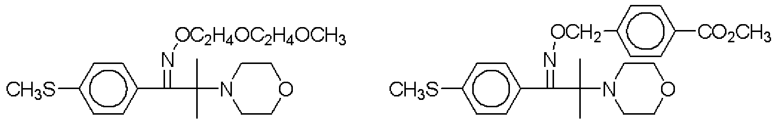


Claims
Priority Applications (4)
| Application Number | Priority Date | Filing Date | Title |
|---|---|---|---|
| KR1020137022216A KR101516613B1 (ko) | 2004-11-30 | 2005-11-24 | 패턴 형성 재료, 및 패턴 형성 장치 및 패턴 형성 방법 |
| KR1020077011922A KR101338091B1 (ko) | 2004-11-30 | 2005-11-24 | 패턴 형성 재료, 및 패턴 형성 장치 및 패턴 형성 방법 |
| CN2005800470449A CN101103310B (zh) | 2004-11-30 | 2005-11-24 | 图案形成材料以及图案形成装置及图案形成方法 |
| KR1020147036965A KR101528784B1 (ko) | 2004-11-30 | 2005-11-24 | 패턴 형성 재료, 및 패턴 형성 장치 및 패턴 형성 방법 |
Applications Claiming Priority (2)
| Application Number | Priority Date | Filing Date | Title |
|---|---|---|---|
| JP2004347638A JP4500657B2 (ja) | 2004-11-30 | 2004-11-30 | パターン形成材料、並びにパターン形成装置及びパターン形成方法 |
| JP2004-347638 | 2004-11-30 |
Publications (1)
| Publication Number | Publication Date |
|---|---|
| WO2006059532A1 true WO2006059532A1 (ja) | 2006-06-08 |
Family
ID=36564966
Family Applications (1)
| Application Number | Title | Priority Date | Filing Date |
|---|---|---|---|
| PCT/JP2005/021589 WO2006059532A1 (ja) | 2004-11-30 | 2005-11-24 | パターン形成材料、並びにパターン形成装置及びパターン形成方法 |
Country Status (5)
| Country | Link |
|---|---|
| JP (1) | JP4500657B2 (ja) |
| KR (3) | KR101528784B1 (ja) |
| CN (1) | CN101103310B (ja) |
| TW (2) | TWI514076B (ja) |
| WO (1) | WO2006059532A1 (ja) |
Cited By (1)
| Publication number | Priority date | Publication date | Assignee | Title |
|---|---|---|---|---|
| WO2007032246A1 (ja) * | 2005-09-16 | 2007-03-22 | Fujifilm Corporation | パターン形成材料、並びにパターン形成装置及びパターン形成方法 |
Families Citing this family (9)
| Publication number | Priority date | Publication date | Assignee | Title |
|---|---|---|---|---|
| JP2006208730A (ja) * | 2005-01-27 | 2006-08-10 | Fuji Photo Film Co Ltd | パターン形成材料、並びにパターン形成装置及びパターン形成方法 |
| TWI546574B (zh) * | 2011-06-01 | 2016-08-21 | Jsr股份有限公司 | 著色組成物、彩色濾光片及顯示元件 |
| WO2014043850A1 (zh) * | 2012-09-18 | 2014-03-27 | 深圳市柔宇科技有限公司 | 一种大尺寸显示屏及其制造方法 |
| JP7308014B2 (ja) * | 2017-02-23 | 2023-07-13 | 旭化成株式会社 | 感光性樹脂組成物及び感光性樹脂積層体 |
| JP6968633B2 (ja) * | 2017-09-07 | 2021-11-17 | 東京応化工業株式会社 | 感光性組成物、及びそれに用いられる光重合開始剤 |
| KR20200112551A (ko) * | 2019-03-22 | 2020-10-05 | 주식회사 엘지화학 | 포토레지스트 제거용 스트리퍼 조성물 및 이를 이용한 포토레지스트의 박리방법 |
| CN114222766A (zh) * | 2019-08-14 | 2022-03-22 | 昭和电工材料株式会社 | 感光性树脂组合物、感光性元件、抗蚀剂图案的形成方法及印刷线路板的制造方法 |
| JP7437212B2 (ja) * | 2020-03-26 | 2024-02-22 | 株式会社オーク製作所 | 露光装置および露光方法 |
| KR102325273B1 (ko) * | 2021-05-07 | 2021-11-10 | 황록연 | 카메라 렌즈용 스페이서 제조방법 및 이로부터 제조되는 스페이서 |
Citations (12)
| Publication number | Priority date | Publication date | Assignee | Title |
|---|---|---|---|---|
| JPH03164742A (ja) * | 1989-09-21 | 1991-07-16 | Hoechst Ag | 照射重合性混合物およびソルダーレジストマスクの製造方法 |
| JPH04240854A (ja) * | 1991-01-25 | 1992-08-28 | Hitachi Chem Co Ltd | 感光性樹脂組成物及びこれを用いた感光性エレメント |
| JPH07199458A (ja) * | 1993-07-22 | 1995-08-04 | E I Du Pont De Nemours & Co | プリント回路のための多層、光画像形成性、水性処理可能なエレメント |
| JP2001159817A (ja) * | 1999-12-03 | 2001-06-12 | Hitachi Chem Co Ltd | 感光性樹脂組成物、これを用いた感光性エレメント、レジストパターンの製造法及びプリント配線板の製造法 |
| JP2001318461A (ja) * | 2000-05-11 | 2001-11-16 | Nichigo Morton Co Ltd | 感光性樹脂組成物およびそれを用いてなる感光性フィルム |
| JP2004126375A (ja) * | 2002-10-04 | 2004-04-22 | Mitsubishi Chemicals Corp | 青紫色レーザー感光性組成物、並びにそれを用いた画像形成材料、画像形成材、及び画像形成方法 |
| JP2004258648A (ja) * | 2003-02-06 | 2004-09-16 | Fuji Photo Film Co Ltd | 感光性平版印刷版 |
| JP2004317851A (ja) * | 2003-04-17 | 2004-11-11 | Hitachi Chem Co Ltd | 感光性樹脂組成物、これを用いた感光性エレメント、レジストパターンの製造方法及びプリント配線板の製造方法 |
| JP2004335639A (ja) * | 2003-05-06 | 2004-11-25 | Fuji Photo Film Co Ltd | 投影露光装置 |
| JP2004335692A (ja) * | 2003-05-07 | 2004-11-25 | Fuji Photo Film Co Ltd | 投影露光装置 |
| JP2005062847A (ja) * | 2003-07-31 | 2005-03-10 | Fuji Photo Film Co Ltd | 露光ヘッド |
| JP2005222039A (ja) * | 2003-12-26 | 2005-08-18 | Fuji Photo Film Co Ltd | 画像露光方法および装置 |
Family Cites Families (1)
| Publication number | Priority date | Publication date | Assignee | Title |
|---|---|---|---|---|
| JP3239881B2 (ja) * | 1998-11-16 | 2001-12-17 | キヤノン株式会社 | 光学系及びそれを用いた投影装置 |
-
2004
- 2004-11-30 JP JP2004347638A patent/JP4500657B2/ja active Active
-
2005
- 2005-11-24 KR KR1020147036965A patent/KR101528784B1/ko active IP Right Grant
- 2005-11-24 KR KR1020077011922A patent/KR101338091B1/ko active IP Right Grant
- 2005-11-24 KR KR1020137022216A patent/KR101516613B1/ko active IP Right Grant
- 2005-11-24 CN CN2005800470449A patent/CN101103310B/zh active Active
- 2005-11-24 WO PCT/JP2005/021589 patent/WO2006059532A1/ja active Application Filing
- 2005-11-29 TW TW102140681A patent/TWI514076B/zh active
- 2005-11-29 TW TW094141826A patent/TWI460541B/zh active
Patent Citations (12)
| Publication number | Priority date | Publication date | Assignee | Title |
|---|---|---|---|---|
| JPH03164742A (ja) * | 1989-09-21 | 1991-07-16 | Hoechst Ag | 照射重合性混合物およびソルダーレジストマスクの製造方法 |
| JPH04240854A (ja) * | 1991-01-25 | 1992-08-28 | Hitachi Chem Co Ltd | 感光性樹脂組成物及びこれを用いた感光性エレメント |
| JPH07199458A (ja) * | 1993-07-22 | 1995-08-04 | E I Du Pont De Nemours & Co | プリント回路のための多層、光画像形成性、水性処理可能なエレメント |
| JP2001159817A (ja) * | 1999-12-03 | 2001-06-12 | Hitachi Chem Co Ltd | 感光性樹脂組成物、これを用いた感光性エレメント、レジストパターンの製造法及びプリント配線板の製造法 |
| JP2001318461A (ja) * | 2000-05-11 | 2001-11-16 | Nichigo Morton Co Ltd | 感光性樹脂組成物およびそれを用いてなる感光性フィルム |
| JP2004126375A (ja) * | 2002-10-04 | 2004-04-22 | Mitsubishi Chemicals Corp | 青紫色レーザー感光性組成物、並びにそれを用いた画像形成材料、画像形成材、及び画像形成方法 |
| JP2004258648A (ja) * | 2003-02-06 | 2004-09-16 | Fuji Photo Film Co Ltd | 感光性平版印刷版 |
| JP2004317851A (ja) * | 2003-04-17 | 2004-11-11 | Hitachi Chem Co Ltd | 感光性樹脂組成物、これを用いた感光性エレメント、レジストパターンの製造方法及びプリント配線板の製造方法 |
| JP2004335639A (ja) * | 2003-05-06 | 2004-11-25 | Fuji Photo Film Co Ltd | 投影露光装置 |
| JP2004335692A (ja) * | 2003-05-07 | 2004-11-25 | Fuji Photo Film Co Ltd | 投影露光装置 |
| JP2005062847A (ja) * | 2003-07-31 | 2005-03-10 | Fuji Photo Film Co Ltd | 露光ヘッド |
| JP2005222039A (ja) * | 2003-12-26 | 2005-08-18 | Fuji Photo Film Co Ltd | 画像露光方法および装置 |
Cited By (1)
| Publication number | Priority date | Publication date | Assignee | Title |
|---|---|---|---|---|
| WO2007032246A1 (ja) * | 2005-09-16 | 2007-03-22 | Fujifilm Corporation | パターン形成材料、並びにパターン形成装置及びパターン形成方法 |
Also Published As
| Publication number | Publication date |
|---|---|
| CN101103310B (zh) | 2012-03-14 |
| CN101103310A (zh) | 2008-01-09 |
| KR101338091B1 (ko) | 2013-12-06 |
| JP4500657B2 (ja) | 2010-07-14 |
| TW201407283A (zh) | 2014-02-16 |
| KR20130101590A (ko) | 2013-09-13 |
| KR101528784B1 (ko) | 2015-06-15 |
| KR101516613B1 (ko) | 2015-05-04 |
| TWI514076B (zh) | 2015-12-21 |
| TW200627067A (en) | 2006-08-01 |
| KR20150009609A (ko) | 2015-01-26 |
| KR20070084581A (ko) | 2007-08-24 |
| TWI460541B (zh) | 2014-11-11 |
| JP2006154556A (ja) | 2006-06-15 |
Similar Documents
| Publication | Publication Date | Title |
|---|---|---|
| JP4966528B2 (ja) | パターン形成材料、並びにパターン形成装置及びパターン形成方法 | |
| WO2006006671A1 (ja) | 感光性組成物、パターン形成材料、感光性積層体、並びにパターン形成装置及びパターン形成方法 | |
| WO2006028060A1 (ja) | パターン形成材料、並びにパターン形成装置及びパターン形成方法 | |
| WO2006059532A1 (ja) | パターン形成材料、並びにパターン形成装置及びパターン形成方法 | |
| WO2005116774A1 (ja) | パターン形成方法 | |
| WO2006059534A1 (ja) | パターン形成材料及びパターン形成方法 | |
| WO2006051761A1 (ja) | パターン形成用組成物及びパターン形成材料、並びに、パターン形成装置及びパターン形成方法 | |
| JP2006163339A (ja) | パターン形成材料、並びにパターン形成装置及びパターン形成方法 | |
| JP2006251385A (ja) | パターン形成材料、並びにパターン形成装置及びパターン形成方法 | |
| JP4546393B2 (ja) | パターン形成材料、並びにパターン形成装置及びパターン形成方法 | |
| JP2007093796A (ja) | パターン形成材料、並びにパターン形成装置及びパターン形成方法 | |
| JP2006251562A (ja) | パターン形成材料、並びにパターン形成装置及びパターン形成方法 | |
| JP2005249970A (ja) | パターン形成材料、並びにパターン形成装置及びパターン形成方法 | |
| WO2006025389A1 (ja) | パターン形成材料、並びにパターン形成装置及びパターン形成方法 | |
| JP2006220858A (ja) | パターン形成材料、並びにパターン形成装置及びパターン形成方法 | |
| JP4942969B2 (ja) | パターン形成材料及びパターン形成方法 | |
| JP5476341B2 (ja) | パターン形成材料、並びにパターン形成装置及びパターン形成方法 | |
| JP4546276B2 (ja) | パターン形成材料、並びにパターン形成装置及びパターン形成方法 | |
| JP2006292889A (ja) | パターン形成材料、並びにパターン形成装置及びパターン形成方法 | |
| JP4451295B2 (ja) | パターン形成方法 | |
| JP2007140174A (ja) | パターン形成材料、並びにパターン形成装置及びパターン形成方法 | |
| JP2006350038A (ja) | パターン形成方法 | |
| JP2006308701A (ja) | パターン形成材料、並びにパターン形成装置及びパターン形成方法 | |
| JP2006003436A (ja) | パターン形成材料、並びにパターン形成装置及びパターン形成方法 | |
| JP2006293039A (ja) | パターン形成材料、並びにパターン形成装置及びパターン形成方法 |
Legal Events
| Date | Code | Title | Description |
|---|---|---|---|
| AK | Designated states |
Kind code of ref document: A1 Designated state(s): AE AG AL AM AT AU AZ BA BB BG BR BW BY BZ CA CH CN CO CR CU CZ DE DK DM DZ EC EE EG ES FI GB GD GE GH GM HR HU ID IL IN IS JP KE KG KM KN KP KR KZ LC LK LR LS LT LU LV LY MA MD MG MK MN MW MX MZ NA NG NI NO NZ OM PG PH PL PT RO RU SC SD SE SG SK SL SM SY TJ TM TN TR TT TZ UA UG US UZ VC VN YU ZA ZM ZW |
|
| AL | Designated countries for regional patents |
Kind code of ref document: A1 Designated state(s): GM KE LS MW MZ NA SD SL SZ TZ UG ZM ZW AM AZ BY KG KZ MD RU TJ TM AT BE BG CH CY CZ DE DK EE ES FI FR GB GR HU IE IS IT LT LU LV MC NL PL PT RO SE SI SK TR BF BJ CF CG CI CM GA GN GQ GW ML MR NE SN TD TG |
|
| 121 | Ep: the epo has been informed by wipo that ep was designated in this application | ||
| WWE | Wipo information: entry into national phase |
Ref document number: 1020077011922 Country of ref document: KR |
|
| NENP | Non-entry into the national phase |
Ref country code: DE |
|
| WWE | Wipo information: entry into national phase |
Ref document number: 200580047044.9 Country of ref document: CN |
|
| 122 | Ep: pct application non-entry in european phase |
Ref document number: 05809262 Country of ref document: EP Kind code of ref document: A1 |
|
| NENP | Non-entry into the national phase |
Ref country code: JP |
|
| WWE | Wipo information: entry into national phase |
Ref document number: 1020137022216 Country of ref document: KR |