WO2006059486A1 - 有機薄膜トランジスタ材料、有機薄膜トランジスタ、電界効果トランジスタ、スイッチング素子、有機半導体材料及び有機半導体膜 - Google Patents
有機薄膜トランジスタ材料、有機薄膜トランジスタ、電界効果トランジスタ、スイッチング素子、有機半導体材料及び有機半導体膜 Download PDFInfo
- Publication number
- WO2006059486A1 WO2006059486A1 PCT/JP2005/021082 JP2005021082W WO2006059486A1 WO 2006059486 A1 WO2006059486 A1 WO 2006059486A1 JP 2005021082 W JP2005021082 W JP 2005021082W WO 2006059486 A1 WO2006059486 A1 WO 2006059486A1
- Authority
- WO
- WIPO (PCT)
- Prior art keywords
- group
- organic
- film transistor
- thin film
- organic thin
- Prior art date
- Legal status (The legal status is an assumption and is not a legal conclusion. Google has not performed a legal analysis and makes no representation as to the accuracy of the status listed.)
- Ceased
Links
Classifications
-
- H—ELECTRICITY
- H10—SEMICONDUCTOR DEVICES; ELECTRIC SOLID-STATE DEVICES NOT OTHERWISE PROVIDED FOR
- H10K—ORGANIC ELECTRIC SOLID-STATE DEVICES
- H10K85/00—Organic materials used in the body or electrodes of devices covered by this subclass
- H10K85/40—Organosilicon compounds, e.g. TIPS pentacene
-
- H—ELECTRICITY
- H10—SEMICONDUCTOR DEVICES; ELECTRIC SOLID-STATE DEVICES NOT OTHERWISE PROVIDED FOR
- H10K—ORGANIC ELECTRIC SOLID-STATE DEVICES
- H10K10/00—Organic devices specially adapted for rectifying, amplifying, oscillating or switching; Organic capacitors or resistors having potential barriers
- H10K10/40—Organic transistors
- H10K10/46—Field-effect transistors, e.g. organic thin-film transistors [OTFT]
- H10K10/462—Insulated gate field-effect transistors [IGFETs]
- H10K10/466—Lateral bottom-gate IGFETs comprising only a single gate
-
- H—ELECTRICITY
- H10—SEMICONDUCTOR DEVICES; ELECTRIC SOLID-STATE DEVICES NOT OTHERWISE PROVIDED FOR
- H10K—ORGANIC ELECTRIC SOLID-STATE DEVICES
- H10K85/00—Organic materials used in the body or electrodes of devices covered by this subclass
- H10K85/30—Coordination compounds
- H10K85/321—Metal complexes comprising a group IIIA element, e.g. Tris (8-hydroxyquinoline) gallium [Gaq3]
- H10K85/322—Metal complexes comprising a group IIIA element, e.g. Tris (8-hydroxyquinoline) gallium [Gaq3] comprising boron
-
- H—ELECTRICITY
- H10—SEMICONDUCTOR DEVICES; ELECTRIC SOLID-STATE DEVICES NOT OTHERWISE PROVIDED FOR
- H10K—ORGANIC ELECTRIC SOLID-STATE DEVICES
- H10K85/00—Organic materials used in the body or electrodes of devices covered by this subclass
- H10K85/60—Organic compounds having low molecular weight
- H10K85/649—Aromatic compounds comprising a hetero atom
-
- H—ELECTRICITY
- H10—SEMICONDUCTOR DEVICES; ELECTRIC SOLID-STATE DEVICES NOT OTHERWISE PROVIDED FOR
- H10K—ORGANIC ELECTRIC SOLID-STATE DEVICES
- H10K85/00—Organic materials used in the body or electrodes of devices covered by this subclass
- H10K85/60—Organic compounds having low molecular weight
- H10K85/649—Aromatic compounds comprising a hetero atom
- H10K85/657—Polycyclic condensed heteroaromatic hydrocarbons
- H10K85/6572—Polycyclic condensed heteroaromatic hydrocarbons comprising only nitrogen in the heteroaromatic polycondensed ring system, e.g. phenanthroline or carbazole
-
- H—ELECTRICITY
- H10—SEMICONDUCTOR DEVICES; ELECTRIC SOLID-STATE DEVICES NOT OTHERWISE PROVIDED FOR
- H10K—ORGANIC ELECTRIC SOLID-STATE DEVICES
- H10K85/00—Organic materials used in the body or electrodes of devices covered by this subclass
- H10K85/60—Organic compounds having low molecular weight
- H10K85/658—Organoboranes
-
- H—ELECTRICITY
- H10—SEMICONDUCTOR DEVICES; ELECTRIC SOLID-STATE DEVICES NOT OTHERWISE PROVIDED FOR
- H10K—ORGANIC ELECTRIC SOLID-STATE DEVICES
- H10K10/00—Organic devices specially adapted for rectifying, amplifying, oscillating or switching; Organic capacitors or resistors having potential barriers
- H10K10/40—Organic transistors
- H10K10/46—Field-effect transistors, e.g. organic thin-film transistors [OTFT]
- H10K10/462—Insulated gate field-effect transistors [IGFETs]
- H10K10/464—Lateral top-gate IGFETs comprising only a single gate
-
- H—ELECTRICITY
- H10—SEMICONDUCTOR DEVICES; ELECTRIC SOLID-STATE DEVICES NOT OTHERWISE PROVIDED FOR
- H10K—ORGANIC ELECTRIC SOLID-STATE DEVICES
- H10K19/00—Integrated devices, or assemblies of multiple devices, comprising at least one organic element specially adapted for rectifying, amplifying, oscillating or switching, covered by group H10K10/00
- H10K19/10—Integrated devices, or assemblies of multiple devices, comprising at least one organic element specially adapted for rectifying, amplifying, oscillating or switching, covered by group H10K10/00 comprising field-effect transistors
-
- H—ELECTRICITY
- H10—SEMICONDUCTOR DEVICES; ELECTRIC SOLID-STATE DEVICES NOT OTHERWISE PROVIDED FOR
- H10K—ORGANIC ELECTRIC SOLID-STATE DEVICES
- H10K85/00—Organic materials used in the body or electrodes of devices covered by this subclass
- H10K85/60—Organic compounds having low molecular weight
- H10K85/615—Polycyclic condensed aromatic hydrocarbons, e.g. anthracene
- H10K85/622—Polycyclic condensed aromatic hydrocarbons, e.g. anthracene containing four rings, e.g. pyrene
-
- H—ELECTRICITY
- H10—SEMICONDUCTOR DEVICES; ELECTRIC SOLID-STATE DEVICES NOT OTHERWISE PROVIDED FOR
- H10K—ORGANIC ELECTRIC SOLID-STATE DEVICES
- H10K85/00—Organic materials used in the body or electrodes of devices covered by this subclass
- H10K85/60—Organic compounds having low molecular weight
- H10K85/615—Polycyclic condensed aromatic hydrocarbons, e.g. anthracene
- H10K85/623—Polycyclic condensed aromatic hydrocarbons, e.g. anthracene containing five rings, e.g. pentacene
-
- H—ELECTRICITY
- H10—SEMICONDUCTOR DEVICES; ELECTRIC SOLID-STATE DEVICES NOT OTHERWISE PROVIDED FOR
- H10K—ORGANIC ELECTRIC SOLID-STATE DEVICES
- H10K85/00—Organic materials used in the body or electrodes of devices covered by this subclass
- H10K85/60—Organic compounds having low molecular weight
- H10K85/649—Aromatic compounds comprising a hetero atom
- H10K85/655—Aromatic compounds comprising a hetero atom comprising only sulfur as heteroatom
Definitions
- Patent Document 2 Japanese Patent Laid-Open No. 5-190877
- Patent Document 3 Japanese Patent Laid-Open No. 8-264805
- Patent Document 5 Japanese Unexamined Patent Publication No. 2003-155289
- Patent Literature 9 Pamphlet of International Publication No. 03Z016599
- Non-Patent Document 2 “Nature” 403ature, 521 pages (2000)
- Non-Patent Document 3 "Advanced Material", 2002, No. 2, page 99
- the present invention has been made in view of the above-mentioned problems, and an object of the present invention is to provide an organic thin film transistor material having good characteristics as a transistor and further capable of suppressing deterioration over time.
- An organic thin film transistor, a field effect transistor, a switching element, an organic semiconductor material and an organic semiconductor film used are provided.
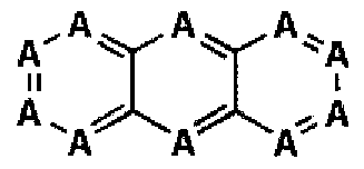
- A is N or C—R (R represents a hydrogen atom, a halogen atom or a substituent, and may be bonded to other R to form a ring).
- R represents a hydrogen atom, a halogen atom or a substituent, and may be bonded to other R to form a ring.
- A has the same meaning as A in the general formula (1), A represents a nonmetallic atom, R
- the organic thin film transistor material according to (6) or (7) is the organic thin film transistor material according to (6) or (7).
- FIG. 2 is an example of a schematic equivalent circuit diagram of the organic TFT of the present invention.
- the organic thin film transistor (TFT) material of the present invention an organic TFT material useful for thin film transistor use is obtained by using the configuration defined in any one of claims 1 to 5. Can do. Further, the organic thin film transistor (TFT) of the present invention produced using the organic TFT material and the field effect transistor of the present invention have high carrier mobility, and the ratio between the maximum current value and the minimum current value when the gate voltage is changed. That is, it was found that the transistor had excellent transistor characteristics such as good ONZOFF characteristics and high durability. In addition, it has been found that a switching element manufactured using the organic TFT or the field effect transistor exhibits good switching characteristics.
- the organic thin film transistor material of the present invention will be described.
- A constitutes a condensed ring formed by a 6-membered aromatic ring or a 6-membered heteroaromatic ring, And C—R, N (nitrogen) or P (phosphorus), and at least one of A is N or P.
- A represents C—R, N or P, and R represents the above
- the support is composed of glass or a flexible resin sheet, and for example, a plastic film can be used as the sheet.
- the plastic film include polyethylene terephthalate (PET), polyethylene naphthalate (PEN), polyethersulfone (PES), polyetherimide, polyetheretherketone, polyphenylenesulfide, polyarylate, polyimide, polycarbonate ( PC), cellulose triacetate (TAC), and cellulose acetate propionate (CAP).
- Comparative compound ⁇ 3> (2, 3, 9, 10-tetrahexylpentacene) was synthesized by the method described in Organic Letters, vol. 2 (2000), p85.
- the organic thin film transistor 614 produced using the organic semiconductor material of the present invention exhibits excellent characteristics in both carrier mobility and ONZOFF ratio immediately after fabrication, and mobility of 10 to 2 or more after the durability test.
- the ratio is more than 10 5 It can be seen that it has little resistance and high durability.
Landscapes
- Chemical & Material Sciences (AREA)
- Engineering & Computer Science (AREA)
- Materials Engineering (AREA)
- Physics & Mathematics (AREA)
- Spectroscopy & Molecular Physics (AREA)
- Inorganic Chemistry (AREA)
- Thin Film Transistor (AREA)
Description


Claims


Priority Applications (3)
| Application Number | Priority Date | Filing Date | Title |
|---|---|---|---|
| US11/720,367 US7800103B2 (en) | 2004-12-02 | 2005-11-17 | Organic thin film transistor material, organic thin film transistor, field-effect transistor, switching element, organic semiconductor material and organic semiconductor film |
| JP2006547740A JPWO2006059486A1 (ja) | 2004-12-02 | 2005-11-17 | 有機薄膜トランジスタ材料、有機薄膜トランジスタ、電界効果トランジスタ、スイッチング素子、有機半導体材料及び有機半導体膜 |
| GB0710324A GB2434918A (en) | 2004-12-02 | 2007-05-30 | Organic thin-film transistor material, organic thin-film transistor, field effect transistor, switching device, organic semiconductor material, and organic |
Applications Claiming Priority (4)
| Application Number | Priority Date | Filing Date | Title |
|---|---|---|---|
| JP2004-349539 | 2004-12-02 | ||
| JP2004349539 | 2004-12-02 | ||
| JP2005-245730 | 2005-08-26 | ||
| JP2005245730 | 2005-08-26 |
Publications (1)
| Publication Number | Publication Date |
|---|---|
| WO2006059486A1 true WO2006059486A1 (ja) | 2006-06-08 |
Family
ID=36564921
Family Applications (1)
| Application Number | Title | Priority Date | Filing Date |
|---|---|---|---|
| PCT/JP2005/021082 Ceased WO2006059486A1 (ja) | 2004-12-02 | 2005-11-17 | 有機薄膜トランジスタ材料、有機薄膜トランジスタ、電界効果トランジスタ、スイッチング素子、有機半導体材料及び有機半導体膜 |
Country Status (4)
| Country | Link |
|---|---|
| US (1) | US7800103B2 (ja) |
| JP (1) | JPWO2006059486A1 (ja) |
| GB (1) | GB2434918A (ja) |
| WO (1) | WO2006059486A1 (ja) |
Cited By (13)
| Publication number | Priority date | Publication date | Assignee | Title |
|---|---|---|---|---|
| WO2007066466A1 (ja) * | 2005-12-06 | 2007-06-14 | Konica Minolta Holdings, Inc. | 有機半導体材料、有機半導体膜、有機半導体デバイス及び有機薄膜トランジスタ |
| WO2007069416A1 (ja) * | 2005-12-13 | 2007-06-21 | Konica Minolta Holdings, Inc. | 有機半導体材料、有機半導体膜、有機半導体デバイス及び有機薄膜トランジスタ |
| WO2007105473A1 (ja) * | 2006-03-10 | 2007-09-20 | Konica Minolta Holdings, Inc. | 有機半導体材料、有機半導体膜、有機半導体デバイス及び有機薄膜トランジスタ |
| JP2008010541A (ja) * | 2006-06-28 | 2008-01-17 | Konica Minolta Holdings Inc | 有機半導体材料、有機半導体膜、有機薄膜トランジスタ及び有機薄膜トランジスタの製造方法 |
| WO2009125705A1 (ja) * | 2008-04-10 | 2009-10-15 | 出光興産株式会社 | 有機薄膜トランジスタ用化合物及びそれを用いた有機薄膜トランジスタ |
| WO2009125721A1 (ja) * | 2008-04-10 | 2009-10-15 | 出光興産株式会社 | 有機薄膜トランジスタ用化合物及び有機薄膜トランジスタ |
| US8101776B2 (en) | 2005-12-12 | 2012-01-24 | Basf Se | Organic semiconductors and their manufacture |
| WO2012067139A1 (ja) * | 2010-11-16 | 2012-05-24 | シャープ株式会社 | 化合物、電界効果トランジスタ及びその製造方法、太陽電池及びその製造方法、有機発光素子及びその製造方法、並びに組成物 |
| JP2014078730A (ja) * | 2013-11-25 | 2014-05-01 | Konica Minolta Inc | 有機半導体材料、有機半導体膜、有機薄膜トランジスタ及び有機薄膜トランジスタの製造方法 |
| JP2014146823A (ja) * | 2014-03-19 | 2014-08-14 | Konica Minolta Inc | 有機半導体材料、有機半導体膜及び有機薄膜トランジスタ |
| JP2015155381A (ja) * | 2014-02-19 | 2015-08-27 | 旭硝子株式会社 | 含フッ素芳香族化合物及びその製造方法 |
| KR20170109413A (ko) * | 2016-03-21 | 2017-09-29 | 주식회사 엘지화학 | 헤테로고리 화합물 및 이를 포함하는 유기 발광 소자 |
| JP2018501634A (ja) * | 2014-09-30 | 2018-01-18 | メルク パテント ゲゼルシャフト ミット ベシュレンクテル ハフツングMerck Patent Gesellschaft mit beschraenkter Haftung | 無機半導体材料および有機結合剤を含む半導体組成物 |
Families Citing this family (9)
| Publication number | Priority date | Publication date | Assignee | Title |
|---|---|---|---|---|
| KR100829743B1 (ko) * | 2005-12-09 | 2008-05-15 | 삼성에스디아이 주식회사 | 유기 박막 트랜지스터 및 이의 제조 방법, 이를 구비한평판 디스플레이 장치 |
| US7517477B2 (en) * | 2006-04-06 | 2009-04-14 | Xerox Corporation | Polydiazaacenes and electronic devices generated therefrom |
| US7517476B2 (en) * | 2006-04-06 | 2009-04-14 | Xerox Corporation | Polydiazaacenes |
| WO2011052285A1 (ja) * | 2009-10-28 | 2011-05-05 | シャープ株式会社 | 新規な化合物、電界効果トランジスタ及び太陽電池ならびにこれらの製造方法、有機半導体層用組成物、ならびにp型半導体層用組成物 |
| JP2017500368A (ja) | 2013-12-24 | 2017-01-05 | ユニバーシティー オブ フロリダ リサーチ ファンデーション, インク. | 抗微生物剤としてのフェナジン誘導体 |
| WO2017011730A2 (en) * | 2015-07-15 | 2017-01-19 | University Of Florida Research Foundation, Incorporated | Phenazine derivatives as antimicrobial agents |
| WO2018152436A1 (en) | 2017-02-17 | 2018-08-23 | University Of Research Foundation, Incorporated | Phenazine derivatives as antimicrobial agents |
| US12060334B2 (en) | 2021-03-12 | 2024-08-13 | University Of Florida Research Foundation, Incorporated | 3-substituted phenazine derivatives as antimicrobial agents |
| CN113555287B (zh) * | 2021-07-22 | 2022-05-24 | 吉林建筑大学 | 一种水分触发降解的p型瞬态薄膜晶体管制备方法 |
Citations (2)
| Publication number | Priority date | Publication date | Assignee | Title |
|---|---|---|---|---|
| JP2003155289A (ja) * | 2001-07-09 | 2003-05-27 | Merck Patent Gmbh | モノ、オリゴおよびポリジチエノピリジンおよびこれらの電荷移動物質としての使用 |
| JP2004179249A (ja) * | 2002-11-25 | 2004-06-24 | Mitsubishi Chemicals Corp | 有機半導体材料及びそれを用いた有機電子デバイス、及び有機電子デバイスの製造方法 |
Family Cites Families (7)
| Publication number | Priority date | Publication date | Assignee | Title |
|---|---|---|---|---|
| EP2199437B1 (en) * | 2001-08-09 | 2015-07-29 | Asahi Kasei Kabushiki Kaisha | Use of an organic semiconductor solution to form oriented polyacene crystals on a substrate |
| US6638644B2 (en) * | 2001-08-28 | 2003-10-28 | Eastman Kodak Company | Electroluminescent devices having diarylanthracene polymers |
| US6686065B2 (en) * | 2001-12-12 | 2004-02-03 | Canon Kabushiki Kaisha | [5]-helicene and dibenzofluorene materials for use in organic light emitting devices |
| JP4522862B2 (ja) * | 2002-11-13 | 2010-08-11 | 株式会社半導体エネルギー研究所 | キノキサリン誘導体、有機半導体素子および電界発光素子 |
| US6849348B2 (en) * | 2002-12-31 | 2005-02-01 | Eastman Kodak Company | Complex fluorene-containing compounds |
| US20040131881A1 (en) * | 2002-12-31 | 2004-07-08 | Eastman Kodak Company | Complex fluorene-containing compounds for use in OLED devices |
| JP2007013097A (ja) * | 2005-06-01 | 2007-01-18 | Sony Corp | 有機半導体材料、有機半導体薄膜及び有機半導体素子 |
-
2005
- 2005-11-17 WO PCT/JP2005/021082 patent/WO2006059486A1/ja not_active Ceased
- 2005-11-17 US US11/720,367 patent/US7800103B2/en not_active Expired - Fee Related
- 2005-11-17 JP JP2006547740A patent/JPWO2006059486A1/ja active Pending
-
2007
- 2007-05-30 GB GB0710324A patent/GB2434918A/en not_active Withdrawn
Patent Citations (2)
| Publication number | Priority date | Publication date | Assignee | Title |
|---|---|---|---|---|
| JP2003155289A (ja) * | 2001-07-09 | 2003-05-27 | Merck Patent Gmbh | モノ、オリゴおよびポリジチエノピリジンおよびこれらの電荷移動物質としての使用 |
| JP2004179249A (ja) * | 2002-11-25 | 2004-06-24 | Mitsubishi Chemicals Corp | 有機半導体材料及びそれを用いた有機電子デバイス、及び有機電子デバイスの製造方法 |
Cited By (17)
| Publication number | Priority date | Publication date | Assignee | Title |
|---|---|---|---|---|
| WO2007066466A1 (ja) * | 2005-12-06 | 2007-06-14 | Konica Minolta Holdings, Inc. | 有機半導体材料、有機半導体膜、有機半導体デバイス及び有機薄膜トランジスタ |
| US8101776B2 (en) | 2005-12-12 | 2012-01-24 | Basf Se | Organic semiconductors and their manufacture |
| WO2007069416A1 (ja) * | 2005-12-13 | 2007-06-21 | Konica Minolta Holdings, Inc. | 有機半導体材料、有機半導体膜、有機半導体デバイス及び有機薄膜トランジスタ |
| WO2007105473A1 (ja) * | 2006-03-10 | 2007-09-20 | Konica Minolta Holdings, Inc. | 有機半導体材料、有機半導体膜、有機半導体デバイス及び有機薄膜トランジスタ |
| JP2008010541A (ja) * | 2006-06-28 | 2008-01-17 | Konica Minolta Holdings Inc | 有機半導体材料、有機半導体膜、有機薄膜トランジスタ及び有機薄膜トランジスタの製造方法 |
| JP5452475B2 (ja) * | 2008-04-10 | 2014-03-26 | 出光興産株式会社 | 有機薄膜トランジスタ用化合物及びそれを用いた有機薄膜トランジスタ |
| WO2009125705A1 (ja) * | 2008-04-10 | 2009-10-15 | 出光興産株式会社 | 有機薄膜トランジスタ用化合物及びそれを用いた有機薄膜トランジスタ |
| WO2009125721A1 (ja) * | 2008-04-10 | 2009-10-15 | 出光興産株式会社 | 有機薄膜トランジスタ用化合物及び有機薄膜トランジスタ |
| JPWO2009125721A1 (ja) * | 2008-04-10 | 2011-08-04 | 出光興産株式会社 | 有機薄膜トランジスタ用化合物及び有機薄膜トランジスタ |
| US8513654B2 (en) | 2008-04-10 | 2013-08-20 | Idemitsu Kosan Co. Ltd. | Compound for organic thin-film transistor and organic thin-film transistor using the compound |
| WO2012067139A1 (ja) * | 2010-11-16 | 2012-05-24 | シャープ株式会社 | 化合物、電界効果トランジスタ及びその製造方法、太陽電池及びその製造方法、有機発光素子及びその製造方法、並びに組成物 |
| JP2014078730A (ja) * | 2013-11-25 | 2014-05-01 | Konica Minolta Inc | 有機半導体材料、有機半導体膜、有機薄膜トランジスタ及び有機薄膜トランジスタの製造方法 |
| JP2015155381A (ja) * | 2014-02-19 | 2015-08-27 | 旭硝子株式会社 | 含フッ素芳香族化合物及びその製造方法 |
| JP2014146823A (ja) * | 2014-03-19 | 2014-08-14 | Konica Minolta Inc | 有機半導体材料、有機半導体膜及び有機薄膜トランジスタ |
| JP2018501634A (ja) * | 2014-09-30 | 2018-01-18 | メルク パテント ゲゼルシャフト ミット ベシュレンクテル ハフツングMerck Patent Gesellschaft mit beschraenkter Haftung | 無機半導体材料および有機結合剤を含む半導体組成物 |
| KR20170109413A (ko) * | 2016-03-21 | 2017-09-29 | 주식회사 엘지화학 | 헤테로고리 화합물 및 이를 포함하는 유기 발광 소자 |
| KR102107874B1 (ko) * | 2016-03-21 | 2020-05-07 | 주식회사 엘지화학 | 헤테로고리 화합물 및 이를 포함하는 유기 발광 소자 |
Also Published As
| Publication number | Publication date |
|---|---|
| JPWO2006059486A1 (ja) | 2008-06-05 |
| US20080121873A1 (en) | 2008-05-29 |
| GB2434918A (en) | 2007-08-08 |
| GB0710324D0 (en) | 2007-07-11 |
| US7800103B2 (en) | 2010-09-21 |
Similar Documents
| Publication | Publication Date | Title |
|---|---|---|
| WO2006059486A1 (ja) | 有機薄膜トランジスタ材料、有機薄膜トランジスタ、電界効果トランジスタ、スイッチング素子、有機半導体材料及び有機半導体膜 | |
| JP2005206750A (ja) | 有機半導体材料、有機トランジスタ、電界効果トランジスタ、スイッチング素子及び5員複素環化合物 | |
| JP5245117B2 (ja) | 有機薄膜トランジスタ、有機半導体材料、有機半導体膜、及び有機半導体デバイス | |
| JP2004006782A (ja) | 有機半導体材料、これを用いた有機トランジスタ、電界効果トランジスタ及びスイッチング素子 | |
| WO2005122278A1 (ja) | 有機半導体薄膜、有機半導体デバイス、有機薄膜トランジスタ及び有機エレクトロルミネッセンス素子 | |
| WO2005122277A1 (ja) | 有機薄膜トランジスタ | |
| WO2005070994A1 (ja) | 有機半導体材料、有機トランジスタ、電界効果トランジスタ、スイッチング素子及びチアゾール化合物 | |
| WO2007123030A1 (ja) | 有機半導体材料、有機半導体膜、有機半導体デバイス及び有機薄膜トランジスタ | |
| JP2006216814A (ja) | 有機半導体材料、有機半導体薄膜、有機薄膜トランジスタ、電界効果トランジスタ及びスイッチング素子 | |
| WO2007105473A1 (ja) | 有機半導体材料、有機半導体膜、有機半導体デバイス及び有機薄膜トランジスタ | |
| JP2007067262A (ja) | 有機半導体材料、有機半導体膜、有機半導体デバイス及び有機薄膜トランジスタ | |
| WO2006054686A1 (ja) | 有機薄膜トランジスタの製造方法及び有機薄膜トランジスタ | |
| JP2004146733A (ja) | 有機半導体及びそれを用いる有機薄膜トランジスタ素子 | |
| JP2006028055A (ja) | 有機半導体材料、有機トランジスタ、電界効果トランジスタ及びスイッチング素子 | |
| JP2006339577A (ja) | 有機半導体薄膜及び有機薄膜トランジスタ | |
| JP2004165257A (ja) | 有機薄膜トランジスタ素子 | |
| WO2006038459A1 (ja) | 有機薄膜トランジスタ材料、有機薄膜トランジスタ、電界効果トランジスタ及びスイッチング素子 | |
| JP2004214482A (ja) | 有機半導体材料および有機薄膜トランジスタ | |
| JP2006165015A (ja) | 有機薄膜トランジスタ材料、有機薄膜トランジスタ、電界効果トランジスタ及びスイッチング素子 | |
| JP5104428B2 (ja) | 有機半導体材料、これを用いた電界効果トランジスタ | |
| JP2006140180A (ja) | 有機薄膜トランジスタ材料、有機薄膜トランジスタ、電界効果トランジスタ及びスイッチング素子 | |
| WO2006098121A1 (ja) | 有機半導体材料、有機半導体膜、有機半導体デバイス、有機薄膜トランジスタ及び有機薄膜トランジスタの形成方法 | |
| JP2006028054A (ja) | 有機薄膜トランジスタ材料、有機薄膜トランジスタ、電界効果トランジスタ及びスイッチング素子 | |
| JP2006222251A (ja) | 有機半導体材料、有機薄膜トランジスタ、電界効果トランジスタ及びスイッチング素子 | |
| JP2004006758A (ja) | 有機半導体材料、これを用いた電界効果トランジスタ及びスイッチング素子 |
Legal Events
| Date | Code | Title | Description |
|---|---|---|---|
| AK | Designated states |
Kind code of ref document: A1 Designated state(s): AE AG AL AM AT AU AZ BA BB BG BR BW BY BZ CA CH CN CO CR CU CZ DE DK DM DZ EC EE EG ES FI GB GD GE GH GM HR HU ID IL IN IS JP KE KG KM KN KP KR KZ LC LK LR LS LT LU LV LY MA MD MG MK MN MW MX MZ NA NG NI NO NZ OM PG PH PL PT RO RU SC SD SE SG SK SL SM SY TJ TM TN TR TT TZ UA UG US UZ VC VN YU ZA ZM ZW |
|
| AL | Designated countries for regional patents |
Kind code of ref document: A1 Designated state(s): GM KE LS MW MZ NA SD SL SZ TZ UG ZM ZW AM AZ BY KG KZ MD RU TJ TM AT BE BG CH CY CZ DE DK EE ES FI FR GB GR HU IE IS IT LT LU LV MC NL PL PT RO SE SI SK TR BF BJ CF CG CI CM GA GN GQ GW ML MR NE SN TD TG |
|
| 121 | Ep: the epo has been informed by wipo that ep was designated in this application | ||
| WWE | Wipo information: entry into national phase |
Ref document number: 2006547740 Country of ref document: JP |
|
| WWE | Wipo information: entry into national phase |
Ref document number: 11720367 Country of ref document: US |
|
| ENP | Entry into the national phase |
Ref document number: 0710324 Country of ref document: GB Kind code of ref document: A Free format text: PCT FILING DATE = 20051117 |
|
| WWE | Wipo information: entry into national phase |
Ref document number: 0710324.5 Country of ref document: GB |
|
| NENP | Non-entry into the national phase |
Ref country code: DE |
|
| REG | Reference to national code |
Ref country code: GB Ref legal event code: 789A Ref document number: 0710324 Country of ref document: GB |
|
| 122 | Ep: pct application non-entry in european phase |
Ref document number: 05806893 Country of ref document: EP Kind code of ref document: A1 |
|
| WWP | Wipo information: published in national office |
Ref document number: 11720367 Country of ref document: US |