US8101776B2 - Organic semiconductors and their manufacture - Google Patents
Organic semiconductors and their manufacture Download PDFInfo
- Publication number
- US8101776B2 US8101776B2 US12/086,157 US8615706A US8101776B2 US 8101776 B2 US8101776 B2 US 8101776B2 US 8615706 A US8615706 A US 8615706A US 8101776 B2 US8101776 B2 US 8101776B2
- Authority
- US
- United States
- Prior art keywords
- substituted
- alkyl
- formula
- unsubstituted
- ring
- Prior art date
- Legal status (The legal status is an assumption and is not a legal conclusion. Google has not performed a legal analysis and makes no representation as to the accuracy of the status listed.)
- Active, expires
Links
- 0 *[n](c1ccccc1c1c(c2c3c4ccccc4[n]2*)C#Cc2ccc[s]2)c1c3C#Cc1ccc[s]1 Chemical compound *[n](c1ccccc1c1c(c2c3c4ccccc4[n]2*)C#Cc2ccc[s]2)c1c3C#Cc1ccc[s]1 0.000 description 30
- IOJUPLGTWVMSFF-UHFFFAOYSA-N C1=CC=C2SC=NC2=C1 Chemical compound C1=CC=C2SC=NC2=C1 IOJUPLGTWVMSFF-UHFFFAOYSA-N 0.000 description 4
- BCMCBBGGLRIHSE-UHFFFAOYSA-N C1=CC=C2OC=NC2=C1 Chemical compound C1=CC=C2OC=NC2=C1 BCMCBBGGLRIHSE-UHFFFAOYSA-N 0.000 description 3
- FCEHBMOGCRZNNI-UHFFFAOYSA-N C1=CC=C2SC=CC2=C1 Chemical compound C1=CC=C2SC=CC2=C1 FCEHBMOGCRZNNI-UHFFFAOYSA-N 0.000 description 3
- XOJHHDZJNXQURY-UHFFFAOYSA-N CC1=CC2=CC3=CC4=C(C=C(C)S4)C=C3C=C2S1.CC1=CC2=NC3=C(C=C(C)C=C3)N=C2C=C1 Chemical compound CC1=CC2=CC3=CC4=C(C=C(C)S4)C=C3C=C2S1.CC1=CC2=NC3=C(C=C(C)C=C3)N=C2C=C1 XOJHHDZJNXQURY-UHFFFAOYSA-N 0.000 description 3
- XCWRSXXZYVRNEA-UHFFFAOYSA-N CC1=CC2=CC3=CC=CC=C3C=C2S1 Chemical compound CC1=CC2=CC3=CC=CC=C3C=C2S1 XCWRSXXZYVRNEA-UHFFFAOYSA-N 0.000 description 3
- XQQBUAPQHNYYRS-UHFFFAOYSA-N CC1=CC=CS1 Chemical compound CC1=CC=CS1 XQQBUAPQHNYYRS-UHFFFAOYSA-N 0.000 description 3
- DXYYSGDWQCSKKO-UHFFFAOYSA-N CC1=NC2=CC=CC=C2S1 Chemical compound CC1=NC2=CC=CC=C2S1 DXYYSGDWQCSKKO-UHFFFAOYSA-N 0.000 description 3
- RDOYJQNOFFENSC-UHFFFAOYSA-N *.B.C.CC.CC.CC1=CC=C(C)C=C1 Chemical compound *.B.C.CC.CC.CC1=CC=C(C)C=C1 RDOYJQNOFFENSC-UHFFFAOYSA-N 0.000 description 2
- FSXSKRIHZCONSN-UHFFFAOYSA-N C/C1=N/C2=CC3=C(C=C2S1)N=CS3 Chemical compound C/C1=N/C2=CC3=C(C=C2S1)N=CS3 FSXSKRIHZCONSN-UHFFFAOYSA-N 0.000 description 2
- KQWIIWBWOABKRG-UHFFFAOYSA-N C1=C/C2=C/C=C3/CC=CC4=CC=C(C1)C2=C43 Chemical compound C1=C/C2=C/C=C3/CC=CC4=CC=C(C1)C2=C43 KQWIIWBWOABKRG-UHFFFAOYSA-N 0.000 description 2
- NIHNNTQXNPWCJQ-UHFFFAOYSA-N C1=CC2=C(C=C1)C1=C(/C=C\C=C/1)C2 Chemical compound C1=CC2=C(C=C1)C1=C(/C=C\C=C/1)C2 NIHNNTQXNPWCJQ-UHFFFAOYSA-N 0.000 description 2
- CYKIHIBNSFRKQP-UHFFFAOYSA-N C1=CC2=CC3=C(C=C2C=C1)SC=C3 Chemical compound C1=CC2=CC3=C(C=C2C=C1)SC=C3 CYKIHIBNSFRKQP-UHFFFAOYSA-N 0.000 description 2
- BBEAQIROQSPTKN-UHFFFAOYSA-N C1=CC2=CC=C3C=CC=C4/C=C\C(=C1)C2=C34 Chemical compound C1=CC2=CC=C3C=CC=C4/C=C\C(=C1)C2=C34 BBEAQIROQSPTKN-UHFFFAOYSA-N 0.000 description 2
- MWPLVEDNUUSJAV-UHFFFAOYSA-N C1=CC=C2C=C3C=CC=CC3=CC2=C1 Chemical compound C1=CC=C2C=C3C=CC=CC3=CC2=C1 MWPLVEDNUUSJAV-UHFFFAOYSA-N 0.000 description 2
- SMWDFEZZVXVKRB-UHFFFAOYSA-N C1=CC=C2N=CC=CC2=C1 Chemical compound C1=CC=C2N=CC=CC2=C1 SMWDFEZZVXVKRB-UHFFFAOYSA-N 0.000 description 2
- JUJWROOIHBZHMG-UHFFFAOYSA-N C1=CC=NC=C1 Chemical compound C1=CC=NC=C1 JUJWROOIHBZHMG-UHFFFAOYSA-N 0.000 description 2
- FZBKIUZHOGZPEQ-UHFFFAOYSA-N CC#CC1=C2C=C3C=C(C)SC3=CC2=C(C#CC)C2=CC3=CC=CC=C3C=C21.CC[Si](C#CC1=C2C=C3C=CSC3=CC2=C(C#C[Si](CC)(CC)CC)C2=CC3=CC=CC=C3C=C21)(CC)CC Chemical compound CC#CC1=C2C=C3C=C(C)SC3=CC2=C(C#CC)C2=CC3=CC=CC=C3C=C21.CC[Si](C#CC1=C2C=C3C=CSC3=CC2=C(C#C[Si](CC)(CC)CC)C2=CC3=CC=CC=C3C=C21)(CC)CC FZBKIUZHOGZPEQ-UHFFFAOYSA-N 0.000 description 2
- WYJOVVXUZNRJQY-UHFFFAOYSA-N CC(=O)C1=CC=CS1 Chemical compound CC(=O)C1=CC=CS1 WYJOVVXUZNRJQY-UHFFFAOYSA-N 0.000 description 2
- RODJECSAAQZOOO-UHFFFAOYSA-N CC.CC.CC1=C2C=C3C=CCC3=CC2=C(C)C2=CC3=CC=CC=C3C=C21 Chemical compound CC.CC.CC1=C2C=C3C=CCC3=CC2=C(C)C2=CC3=CC=CC=C3C=C21 RODJECSAAQZOOO-UHFFFAOYSA-N 0.000 description 2
- LUPFCHBFHZLESM-UHFFFAOYSA-N CC1=CC2=C(C=CN2C)N1C Chemical compound CC1=CC2=C(C=CN2C)N1C LUPFCHBFHZLESM-UHFFFAOYSA-N 0.000 description 2
- KGXXEMQGLOTQGJ-UHFFFAOYSA-N CC1=CC2=C(C=CS2)N1C Chemical compound CC1=CC2=C(C=CS2)N1C KGXXEMQGLOTQGJ-UHFFFAOYSA-N 0.000 description 2
- REFXKVVKFBUOND-UHFFFAOYSA-N CC1=CC2=C(C=CS2)S1 Chemical compound CC1=CC2=C(C=CS2)S1 REFXKVVKFBUOND-UHFFFAOYSA-N 0.000 description 2
- UBJYOVRJNZYLIT-UHFFFAOYSA-N CC1=CC2=C(S1)C1=C(C=CS1)S2 Chemical compound CC1=CC2=C(S1)C1=C(C=CS1)S2 UBJYOVRJNZYLIT-UHFFFAOYSA-N 0.000 description 2
- QIMMUPPBPVKWKM-UHFFFAOYSA-N CC1=CC2=CC=CC=C2C=C1 Chemical compound CC1=CC2=CC=CC=C2C=C1 QIMMUPPBPVKWKM-UHFFFAOYSA-N 0.000 description 2
- YXFVVABEGXRONW-UHFFFAOYSA-N CC1=CC=CC=C1 Chemical compound CC1=CC=CC=C1 YXFVVABEGXRONW-UHFFFAOYSA-N 0.000 description 2
- PBHUHWMTDYWBRD-UHFFFAOYSA-N CC1=NC2=C(N=CS2)S1 Chemical compound CC1=NC2=C(N=CS2)S1 PBHUHWMTDYWBRD-UHFFFAOYSA-N 0.000 description 2
- SRXLWXSDRJCBNV-UHFFFAOYSA-N CC1=NC2=NC=NC2=N1 Chemical compound CC1=NC2=NC=NC2=N1 SRXLWXSDRJCBNV-UHFFFAOYSA-N 0.000 description 2
- YGPWFAWENNBZQA-UHFFFAOYSA-N CC1=NN=CC1 Chemical compound CC1=NN=CC1 YGPWFAWENNBZQA-UHFFFAOYSA-N 0.000 description 2
- OOINHEJXCMGEHS-UHFFFAOYSA-N CC[Si](C#CC1=C2C=C3C=CSC3=CC2=C(C#C[Si](CC)(CC)CC)C2=CC3=CC=CC=C3C=C21)(CC)CC Chemical compound CC[Si](C#CC1=C2C=C3C=CSC3=CC2=C(C#C[Si](CC)(CC)CC)C2=CC3=CC=CC=C3C=C21)(CC)CC OOINHEJXCMGEHS-UHFFFAOYSA-N 0.000 description 2
- FGYADSCZTQOAFK-UHFFFAOYSA-N CN1C=NC2=CC=CC=C21 Chemical compound CN1C=NC2=CC=CC=C21 FGYADSCZTQOAFK-UHFFFAOYSA-N 0.000 description 2
- WACNXHCZHTVBJM-UHFFFAOYSA-N FC1=CC(F)=C(F)C(F)=C1F Chemical compound FC1=CC(F)=C(F)C(F)=C1F WACNXHCZHTVBJM-UHFFFAOYSA-N 0.000 description 2
- WMDJEMWYLFYWME-UHFFFAOYSA-N O=C1C2=C(C=C3C=CC=CC3=C2)C(=O)C2=C1C=C1C=CSC1=C2 Chemical compound O=C1C2=C(C=C3C=CC=CC3=C2)C(=O)C2=C1C=C1C=CSC1=C2 WMDJEMWYLFYWME-UHFFFAOYSA-N 0.000 description 2
- WRHZVMBBRYBTKZ-UHFFFAOYSA-N OC(c1ccc[nH]1)=O Chemical compound OC(c1ccc[nH]1)=O WRHZVMBBRYBTKZ-UHFFFAOYSA-N 0.000 description 2
- SJDNYLZCJZKLME-UHFFFAOYSA-N *.B.C.CC.CC.CC.CC.CC Chemical compound *.B.C.CC.CC.CC.CC.CC SJDNYLZCJZKLME-UHFFFAOYSA-N 0.000 description 1
- VLYIJQRFZYCMGI-UHFFFAOYSA-N B.B.C.C.C.CC.CC.CC.CC.O=C1C=CC(=O)C2=CC=CC=C12.O=C1C=CC(=O)C2=CC=CC=C12 Chemical compound B.B.C.C.C.CC.CC.CC.CC.O=C1C=CC(=O)C2=CC=CC=C12.O=C1C=CC(=O)C2=CC=CC=C12 VLYIJQRFZYCMGI-UHFFFAOYSA-N 0.000 description 1
- ZIIGCMQLOXLSDY-UHFFFAOYSA-N B.B.C.C.C=C.CC.CC.CC.CC.I[IH]I.O=C1C=CC(=O)C=C1.O=C1C=CC(=O)O1 Chemical compound B.B.C.C.C=C.CC.CC.CC.CC.I[IH]I.O=C1C=CC(=O)C=C1.O=C1C=CC(=O)O1 ZIIGCMQLOXLSDY-UHFFFAOYSA-N 0.000 description 1
- DMGFKARDEWRRNZ-UHFFFAOYSA-N B.C.CC.CC.CC.CC.CC.[Y]C1=C2C=CC=CC2=C([Y])C2=CC=CC=C21 Chemical compound B.C.CC.CC.CC.CC.CC.[Y]C1=C2C=CC=CC2=C([Y])C2=CC=CC=C21 DMGFKARDEWRRNZ-UHFFFAOYSA-N 0.000 description 1
- DDDSREQSOKYYEO-UHFFFAOYSA-N B.C.CC.CC.CC.I Chemical compound B.C.CC.CC.CC.I DDDSREQSOKYYEO-UHFFFAOYSA-N 0.000 description 1
- LJOOFAFKJSMTQJ-UHFFFAOYSA-N B.C.CC.CC.CC1(O)C=CC(C)(O)C=C1 Chemical compound B.C.CC.CC.CC1(O)C=CC(C)(O)C=C1 LJOOFAFKJSMTQJ-UHFFFAOYSA-N 0.000 description 1
- QGYCHAVIXJAZHS-UHFFFAOYSA-N B.C.CC.CC.O=C1C=CC(=O)C=C1 Chemical compound B.C.CC.CC.O=C1C=CC(=O)C=C1 QGYCHAVIXJAZHS-UHFFFAOYSA-N 0.000 description 1
- ODJLELWUSYLXPS-UHFFFAOYSA-N BrC1=C2C=CC=CC2=C(Br)C2=CC=CC=C21.CC.CC Chemical compound BrC1=C2C=CC=CC2=C(Br)C2=CC=CC=C21.CC.CC ODJLELWUSYLXPS-UHFFFAOYSA-N 0.000 description 1
- FJJSKDFNLYWVRY-UHFFFAOYSA-N BrC1=CC2=NC3=C(C=C(Br)C=C3)N=C2C=C1.CC1=CC2=CC3=CC4=C(C=C(C)S4)C=C3C=C2S1.CC1=CC2=CC3=CC4=C(C=C(C)S4)C=C3C=C2S1.[Y]C1=CC2=NC3=C(C=C([Y])C=C3)N=C2C=C1 Chemical compound BrC1=CC2=NC3=C(C=C(Br)C=C3)N=C2C=C1.CC1=CC2=CC3=CC4=C(C=C(C)S4)C=C3C=C2S1.CC1=CC2=CC3=CC4=C(C=C(C)S4)C=C3C=C2S1.[Y]C1=CC2=NC3=C(C=C([Y])C=C3)N=C2C=C1 FJJSKDFNLYWVRY-UHFFFAOYSA-N 0.000 description 1
- LPFXHGPJXIYUCA-UHFFFAOYSA-N BrC1=CC=C(C#CC2=C3C=CC=CC3=C(C#CC3=CC=C(Br)C=C3)C3=CC=CC=C32)C=C1 Chemical compound BrC1=CC=C(C#CC2=C3C=CC=CC3=C(C#CC3=CC=C(Br)C=C3)C3=CC=CC=C32)C=C1 LPFXHGPJXIYUCA-UHFFFAOYSA-N 0.000 description 1
- OMUQBOVKZXWIEY-UHFFFAOYSA-N C(#CC1=C2C3=C(C=CC=C3)N(CC3=CC=CC=C3)C2=C(C#CC2=CC=CS2)C2=C1N(CC1=CC=CC=C1)C1=C2C=CC=C1)C1=CC=CS1.C(#CC1=C2OC3=C(C=CC=C3)C2=C(C#CC2=CC3=C(C=C4C=CC=CC4=C3)S2)C2=C1C1=C(C=CC=C1)O2)C1=CC2=C(C=C3C=CC=CC3=C2)S1.CC(C)[Si](C#C/C1=C2\SC3=C(SC(C4=CC=CC=C4)=C3)\C2=C(/C#C[Si](C(C)C)(C(C)C)C(C)C)C2=C1C1=C(C=C(C3=CC=CC=C3)S1)S2)(C(C)C)C(C)C.CCCCCCCCCCCCC#CC1=C2C=C3C=CSC3=CC2=C(C#CCCCCCCCCCCCC)C2=CC3=C(C=C21)SC=C3 Chemical compound C(#CC1=C2C3=C(C=CC=C3)N(CC3=CC=CC=C3)C2=C(C#CC2=CC=CS2)C2=C1N(CC1=CC=CC=C1)C1=C2C=CC=C1)C1=CC=CS1.C(#CC1=C2OC3=C(C=CC=C3)C2=C(C#CC2=CC3=C(C=C4C=CC=CC4=C3)S2)C2=C1C1=C(C=CC=C1)O2)C1=CC2=C(C=C3C=CC=CC3=C2)S1.CC(C)[Si](C#C/C1=C2\SC3=C(SC(C4=CC=CC=C4)=C3)\C2=C(/C#C[Si](C(C)C)(C(C)C)C(C)C)C2=C1C1=C(C=C(C3=CC=CC=C3)S1)S2)(C(C)C)C(C)C.CCCCCCCCCCCCC#CC1=C2C=C3C=CSC3=CC2=C(C#CCCCCCCCCCCCC)C2=CC3=C(C=C21)SC=C3 OMUQBOVKZXWIEY-UHFFFAOYSA-N 0.000 description 1
- LENYJGPBCXFGCJ-UHFFFAOYSA-N C(#CC1=C2C=C3C=CSC3=CC2=C(C#CC2=CC3=CC=CC=C3C=C2)C2=CC3C=CSC3C=C21)C1=CC2=CC=CC=C2C=C1.CCCCCCC1=CC=C(C#CC2=C3C=C4N=CC=C(CCCCCC)C4=CC3=C(C#CC3=CC=C(CCCCCC)S3)C3=CC4=NC=CC(CCCCCC)=C4C=C32)S1.CCCCCCCCC1=CC2=C(C=C1CCCCCCCC)C1=C(C#CC3=CC=C(C(C)(C)C)C=C3)C3=C(C(C#CC4=CC=C(C(C)(C)C)C=C4)=C1S2)C1=C(C=C(CCCCCCCC)C(CCCCCCCC)=C1)S3 Chemical compound C(#CC1=C2C=C3C=CSC3=CC2=C(C#CC2=CC3=CC=CC=C3C=C2)C2=CC3C=CSC3C=C21)C1=CC2=CC=CC=C2C=C1.CCCCCCC1=CC=C(C#CC2=C3C=C4N=CC=C(CCCCCC)C4=CC3=C(C#CC3=CC=C(CCCCCC)S3)C3=CC4=NC=CC(CCCCCC)=C4C=C32)S1.CCCCCCCCC1=CC2=C(C=C1CCCCCCCC)C1=C(C#CC3=CC=C(C(C)(C)C)C=C3)C3=C(C(C#CC4=CC=C(C(C)(C)C)C=C4)=C1S2)C1=C(C=C(CCCCCCCC)C(CCCCCCCC)=C1)S3 LENYJGPBCXFGCJ-UHFFFAOYSA-N 0.000 description 1
- JITGZQKVYFUDRH-UHFFFAOYSA-N C(#CC1=C2SC3=C(C=C4C=CC=CC4=C3)C2=C(C#CC2=CC3=CC4=CC=CC=C4C=C3C=C2)C2=C1C1=C(C=C3C=CC=CC3=C1)S2)C1=CC2=CC3=CC=CC=C3C=C2C=C1.CCCCCCC1=CC=C(C#CC2=C3C=C4N=CC=C(CCCCCC)C4=CC3=C(C#CC3=CC=C(CCCCCC)S3)C3=CC4=NC=CC(CCCCCC)=C4C=C32)S1.CCCCCCCCCCCCC1=CC2=CC3=C(C#CC4=NC5=C(C=CC=C5)S4)C4=CC5=C(C=C(CCCCCCCCCCCC)S5)C=C4C(C#CC4=NC5=C(C=CC=C5)S4)=C3C=C2S1.O=C(C#CC#CC#CC(F)(F)(F)(F)(F)(F)(F)(F)(F)(F)(F)(F)(F)(F)F)C1=CC2=CC3=C(C#CC4=C(F)C(F)=C(F)C(F)=C4F)C4=CC5=CC=CC=C5C=C4C(C#CC4=C(F)C(F)=C(F)C(F)=C4F)=C3C=C2S1 Chemical compound C(#CC1=C2SC3=C(C=C4C=CC=CC4=C3)C2=C(C#CC2=CC3=CC4=CC=CC=C4C=C3C=C2)C2=C1C1=C(C=C3C=CC=CC3=C1)S2)C1=CC2=CC3=CC=CC=C3C=C2C=C1.CCCCCCC1=CC=C(C#CC2=C3C=C4N=CC=C(CCCCCC)C4=CC3=C(C#CC3=CC=C(CCCCCC)S3)C3=CC4=NC=CC(CCCCCC)=C4C=C32)S1.CCCCCCCCCCCCC1=CC2=CC3=C(C#CC4=NC5=C(C=CC=C5)S4)C4=CC5=C(C=C(CCCCCCCCCCCC)S5)C=C4C(C#CC4=NC5=C(C=CC=C5)S4)=C3C=C2S1.O=C(C#CC#CC#CC(F)(F)(F)(F)(F)(F)(F)(F)(F)(F)(F)(F)(F)(F)F)C1=CC2=CC3=C(C#CC4=C(F)C(F)=C(F)C(F)=C4F)C4=CC5=CC=CC=C5C=C4C(C#CC4=C(F)C(F)=C(F)C(F)=C4F)=C3C=C2S1 JITGZQKVYFUDRH-UHFFFAOYSA-N 0.000 description 1
- KLGDINDBRWFABJ-UHFFFAOYSA-N C.C.C.C.C.C.CC.CC.CC.CC.O=C1C2=CC=CC=C2C(=O)C2=C1C=CC=C2.O=C1C2=CC=CC=C2C(=O)C2=C1C=CC=C2 Chemical compound C.C.C.C.C.C.CC.CC.CC.CC.O=C1C2=CC=CC=C2C(=O)C2=C1C=CC=C2.O=C1C2=CC=CC=C2C(=O)C2=C1C=CC=C2 KLGDINDBRWFABJ-UHFFFAOYSA-N 0.000 description 1
- RPSCCLFSVCRHKU-UHFFFAOYSA-N C.CC(C)[Si](C#CC1=C2SC3=C(C=CC=C3)C2=C(C#C[Si](C(C)C)(C(C)C)C(C)C)C2=C1C1=C(C=CC=C1)S2)(C(C)C)C(C)C Chemical compound C.CC(C)[Si](C#CC1=C2SC3=C(C=CC=C3)C2=C(C#C[Si](C(C)C)(C(C)C)C(C)C)C2=C1C1=C(C=CC=C1)S2)(C(C)C)C(C)C RPSCCLFSVCRHKU-UHFFFAOYSA-N 0.000 description 1
- HLSFEVPVENXEFL-UHFFFAOYSA-N C.CC.OC1=CC=C(O)C=C1 Chemical compound C.CC.OC1=CC=C(O)C=C1 HLSFEVPVENXEFL-UHFFFAOYSA-N 0.000 description 1
- UQEOQQMFSWSQNG-UAIGNFCESA-N C.CC.[H]C(=O)/C=C\C([H])=O Chemical compound C.CC.[H]C(=O)/C=C\C([H])=O UQEOQQMFSWSQNG-UAIGNFCESA-N 0.000 description 1
- VJYJJHQEVLEOFL-UHFFFAOYSA-N C1=CC2=C(/C=C\S2)S1 Chemical compound C1=CC2=C(/C=C\S2)S1 VJYJJHQEVLEOFL-UHFFFAOYSA-N 0.000 description 1
- TXCDCPKCNAJMEE-UHFFFAOYSA-N C1=CC2=C(C=C1)C1=C(/C=C\C=C/1)O2 Chemical compound C1=CC2=C(C=C1)C1=C(/C=C\C=C/1)O2 TXCDCPKCNAJMEE-UHFFFAOYSA-N 0.000 description 1
- IYYZUPMFVPLQIF-UHFFFAOYSA-N C1=CC2=C(C=C1)C1=C(/C=C\C=C/1)S2 Chemical compound C1=CC2=C(C=C1)C1=C(/C=C\C=C/1)S2 IYYZUPMFVPLQIF-UHFFFAOYSA-N 0.000 description 1
- HYZJCKYKOHLVJF-UHFFFAOYSA-N C1=CC2=C(C=C1)NC=N2 Chemical compound C1=CC2=C(C=C1)NC=N2 HYZJCKYKOHLVJF-UHFFFAOYSA-N 0.000 description 1
- VGWBXRXNERKBSJ-UHFFFAOYSA-N C1=CC2=C(S1)C1=C(/C=C\S1)S2 Chemical compound C1=CC2=C(S1)C1=C(/C=C\S1)S2 VGWBXRXNERKBSJ-UHFFFAOYSA-N 0.000 description 1
- UOBSRIGNYWMYGH-UHFFFAOYSA-N C1=CC2=CC3=C(C=C2C=C1)SC=C3.C1=CC=C2SC=CC2=C1.C1=CSC=C1 Chemical compound C1=CC2=CC3=C(C=C2C=C1)SC=C3.C1=CC=C2SC=CC2=C1.C1=CSC=C1 UOBSRIGNYWMYGH-UHFFFAOYSA-N 0.000 description 1
- URMVZUQDPPDABD-UHFFFAOYSA-N C1=CC2=CC3=C(C=CS3)C=C2S1 Chemical compound C1=CC2=CC3=C(C=CS3)C=C2S1 URMVZUQDPPDABD-UHFFFAOYSA-N 0.000 description 1
- LMIZORQOLSLQRY-UHFFFAOYSA-N C1=CC=C2/C=C\C=C/C2=C1.C1=CC=CC=C1 Chemical compound C1=CC=C2/C=C\C=C/C2=C1.C1=CC=CC=C1 LMIZORQOLSLQRY-UHFFFAOYSA-N 0.000 description 1
- LSNAXNVALAUNRR-UHFFFAOYSA-N C1=CC=C2/C=C\C=C/C2=C1.C1=CC=CC=C1.CC.CC Chemical compound C1=CC=C2/C=C\C=C/C2=C1.C1=CC=CC=C1.CC.CC LSNAXNVALAUNRR-UHFFFAOYSA-N 0.000 description 1
- UJOBWOGCFQCDNV-UHFFFAOYSA-N C1=CC=C2C(=C1)NC1=C2C=CC=C1 Chemical compound C1=CC=C2C(=C1)NC1=C2C=CC=C1 UJOBWOGCFQCDNV-UHFFFAOYSA-N 0.000 description 1
- UFWIBTONFRDIAS-UHFFFAOYSA-N C1=CC=C2C=CC=CC2=C1 Chemical compound C1=CC=C2C=CC=CC2=C1 UFWIBTONFRDIAS-UHFFFAOYSA-N 0.000 description 1
- DZBUGLKDJFMEHC-UHFFFAOYSA-N C1=CC=C2N=C3C=CC=CC3=CC2=C1 Chemical compound C1=CC=C2N=C3C=CC=CC3=CC2=C1 DZBUGLKDJFMEHC-UHFFFAOYSA-N 0.000 description 1
- XSCHRSMBECNVNS-UHFFFAOYSA-N C1=CC=C2N=CC=NC2=C1 Chemical compound C1=CC=C2N=CC=NC2=C1 XSCHRSMBECNVNS-UHFFFAOYSA-N 0.000 description 1
- SIKJAQJRHWYJAI-UHFFFAOYSA-N C1=CC=C2NC=CC2=C1 Chemical compound C1=CC=C2NC=CC2=C1 SIKJAQJRHWYJAI-UHFFFAOYSA-N 0.000 description 1
- QRUDEWIWKLJBPS-UHFFFAOYSA-N C1=CC=C2NN=NC2=C1 Chemical compound C1=CC=C2NN=NC2=C1 QRUDEWIWKLJBPS-UHFFFAOYSA-N 0.000 description 1
- IANQTJSKSUMEQM-UHFFFAOYSA-N C1=CC=C2OC=CC2=C1 Chemical compound C1=CC=C2OC=CC2=C1 IANQTJSKSUMEQM-UHFFFAOYSA-N 0.000 description 1
- ZSWFCLXCOIISFI-UHFFFAOYSA-N C1=CCC=C1 Chemical compound C1=CCC=C1 ZSWFCLXCOIISFI-UHFFFAOYSA-N 0.000 description 1
- VXIKDBJPBRMXBP-UHFFFAOYSA-N C1=CN=CC1 Chemical compound C1=CN=CC1 VXIKDBJPBRMXBP-UHFFFAOYSA-N 0.000 description 1
- KYQCOXFCLRTKLS-UHFFFAOYSA-N C1=CN=CC=N1 Chemical compound C1=CN=CC=N1 KYQCOXFCLRTKLS-UHFFFAOYSA-N 0.000 description 1
- CZPWVGJYEJSRLH-UHFFFAOYSA-N C1=CN=CN=C1 Chemical compound C1=CN=CN=C1 CZPWVGJYEJSRLH-UHFFFAOYSA-N 0.000 description 1
- PBMFSQRYOILNGV-UHFFFAOYSA-N C1=CN=NC=C1 Chemical compound C1=CN=NC=C1 PBMFSQRYOILNGV-UHFFFAOYSA-N 0.000 description 1
- KAESVJOAVNADME-UHFFFAOYSA-N C1=CNC=C1 Chemical compound C1=CNC=C1 KAESVJOAVNADME-UHFFFAOYSA-N 0.000 description 1
- RAXXELZNTBOGNW-UHFFFAOYSA-N C1=CNC=N1 Chemical compound C1=CNC=N1 RAXXELZNTBOGNW-UHFFFAOYSA-N 0.000 description 1
- YLQBMQCUIZJEEH-UHFFFAOYSA-N C1=COC=C1 Chemical compound C1=COC=C1 YLQBMQCUIZJEEH-UHFFFAOYSA-N 0.000 description 1
- ZCQWOFVYLHDMMC-UHFFFAOYSA-N C1=COC=N1 Chemical compound C1=COC=N1 ZCQWOFVYLHDMMC-UHFFFAOYSA-N 0.000 description 1
- YTPLMLYBLZKORZ-UHFFFAOYSA-N C1=CSC=C1 Chemical compound C1=CSC=C1 YTPLMLYBLZKORZ-UHFFFAOYSA-N 0.000 description 1
- FZWLAAWBMGSTSO-UHFFFAOYSA-N C1=CSC=N1 Chemical compound C1=CSC=N1 FZWLAAWBMGSTSO-UHFFFAOYSA-N 0.000 description 1
- POQXSXLBPPFJFO-UHFFFAOYSA-N C1=NC2=C(N=CS2)S1 Chemical compound C1=NC2=C(N=CS2)S1 POQXSXLBPPFJFO-UHFFFAOYSA-N 0.000 description 1
- JWLNXHODHNBWPR-UHFFFAOYSA-N C1=NC2=CC3=C(C=C2S1)N=CS3 Chemical compound C1=NC2=CC3=C(C=C2S1)N=CS3 JWLNXHODHNBWPR-UHFFFAOYSA-N 0.000 description 1
- KJUGUADJHNHALS-UHFFFAOYSA-N C1=NN=NN1 Chemical compound C1=NN=NN1 KJUGUADJHNHALS-UHFFFAOYSA-N 0.000 description 1
- FDRJORFCEVZMJO-UHFFFAOYSA-N C1CCNCC1.CC.CC.CC.CC.CC1=C2C=CC=CC2=C(C)C2=C1C=CC=C2.CC1=C2C=CC=CC2=C(C)C2=C1C=CC=C2.[H]C Chemical compound C1CCNCC1.CC.CC.CC.CC.CC1=C2C=CC=CC2=C(C)C2=C1C=CC=C2.CC1=C2C=CC=CC2=C(C)C2=C1C=CC=C2.[H]C FDRJORFCEVZMJO-UHFFFAOYSA-N 0.000 description 1
- NWQOOCZUHISVOM-UHFFFAOYSA-N CC(C)(C)C1=CC=C(C#CC2(O)C3=C(C4=C(C=CC=C4)S3)C(O)(C#CC3=CC=C(C(C)(C)C)C=C3)C3=C2C2=C(C=CC=C2)S3)C=C1 Chemical compound CC(C)(C)C1=CC=C(C#CC2(O)C3=C(C4=C(C=CC=C4)S3)C(O)(C#CC3=CC=C(C(C)(C)C)C=C3)C3=C2C2=C(C=CC=C2)S3)C=C1 NWQOOCZUHISVOM-UHFFFAOYSA-N 0.000 description 1
- OFAPOTHMRUSWPP-UHFFFAOYSA-N CC(C)(C)C1=CC=C(C#CC2=C3SC4=C(C=CC=C4)C3=C(C#CC3=CC=C(C(C)(C)C)C=C3)C3=C2C2=C(C=CC=C2)S3)C=C1 Chemical compound CC(C)(C)C1=CC=C(C#CC2=C3SC4=C(C=CC=C4)C3=C(C#CC3=CC=C(C(C)(C)C)C=C3)C3=C2C2=C(C=CC=C2)S3)C=C1 OFAPOTHMRUSWPP-UHFFFAOYSA-N 0.000 description 1
- GORYEFFIZYZRLL-UHFFFAOYSA-N CC(C)(C)C1=CC=CC=C1.FC1=CC=CC(F)=C1 Chemical compound CC(C)(C)C1=CC=CC=C1.FC1=CC=CC(F)=C1 GORYEFFIZYZRLL-UHFFFAOYSA-N 0.000 description 1
- NNPPMTNAJDCUHE-UHFFFAOYSA-N CC(C)C Chemical compound CC(C)C NNPPMTNAJDCUHE-UHFFFAOYSA-N 0.000 description 1
- ZQGWKVNOMDHWAJ-UHFFFAOYSA-N CC(C)[Si](C#CC1(O)C2=C(C3=C(C=CC=C3)S2)C(O)(C#C[Si](C(C)C)(C(C)C)C(C)C)C2=C1C1=C(C=CC=C1)S2)(C(C)C)C(C)C Chemical compound CC(C)[Si](C#CC1(O)C2=C(C3=C(C=CC=C3)S2)C(O)(C#C[Si](C(C)C)(C(C)C)C(C)C)C2=C1C1=C(C=CC=C1)S2)(C(C)C)C(C)C ZQGWKVNOMDHWAJ-UHFFFAOYSA-N 0.000 description 1
- OACULYOOBDLRMR-UHFFFAOYSA-N CC(C)[Si](C#CC1=C2C=C3C=CSC3=CC2=C(C#C[Si](C(C)C)(C(C)C)C(C)C)C2=CC3=CC=CC=C3C=C21)(C(C)C)C(C)C Chemical compound CC(C)[Si](C#CC1=C2C=C3C=CSC3=CC2=C(C#C[Si](C(C)C)(C(C)C)C(C)C)C2=CC3=CC=CC=C3C=C21)(C(C)C)C(C)C OACULYOOBDLRMR-UHFFFAOYSA-N 0.000 description 1
- NASSKUMBCLXSKK-UHFFFAOYSA-N CC(C)[Si](C#CC1=C2N=C3C=CC=CC3=NC2=C(C#C[Si](C(C)C)(C(C)C)C(C)C)C2=NC3=C(C=CC=C3)N=C21)(C(C)C)C(C)C Chemical compound CC(C)[Si](C#CC1=C2N=C3C=CC=CC3=NC2=C(C#C[Si](C(C)C)(C(C)C)C(C)C)C2=NC3=C(C=CC=C3)N=C21)(C(C)C)C(C)C NASSKUMBCLXSKK-UHFFFAOYSA-N 0.000 description 1
- BHUJRVDUVQGEGQ-UHFFFAOYSA-N CC(C)[Si](C#CC1=C2SC3=C(C=CC=C3)C2=C(C#C[Si](C(C)C)(C(C)C)C(C)C)C2=C1C1=C(C=CC=C1)S2)(C(C)C)C(C)C Chemical compound CC(C)[Si](C#CC1=C2SC3=C(C=CC=C3)C2=C(C#C[Si](C(C)C)(C(C)C)C(C)C)C2=C1C1=C(C=CC=C1)S2)(C(C)C)C(C)C BHUJRVDUVQGEGQ-UHFFFAOYSA-N 0.000 description 1
- WDKZHTQVKBUNQY-UCPSEBEXSA-N CC.CC.CC1=C2[2H]C3=CC=CC=C3C2=C(C)C2=C1C1=C(C=CC=C1)C2 Chemical compound CC.CC.CC1=C2[2H]C3=CC=CC=C3C2=C(C)C2=C1C1=C(C=CC=C1)C2 WDKZHTQVKBUNQY-UCPSEBEXSA-N 0.000 description 1
- UKFZBDAYBNZPTR-PSTFXIMESA-N CC.CC.CC1=C2[2H]C3=CC=CC=C3C2=C(C)C2=C1C1=C([2H]2)C=CC=C1 Chemical compound CC.CC.CC1=C2[2H]C3=CC=CC=C3C2=C(C)C2=C1C1=C([2H]2)C=CC=C1 UKFZBDAYBNZPTR-PSTFXIMESA-N 0.000 description 1
- RNYXGYCLKXDQDH-UHFFFAOYSA-N CC.CC.O=C1C2=C(C=CC=C2)C(=O)C2=C1C=CC=C2 Chemical compound CC.CC.O=C1C2=C(C=CC=C2)C(=O)C2=C1C=CC=C2 RNYXGYCLKXDQDH-UHFFFAOYSA-N 0.000 description 1
- CDJNRJHNRFRYCQ-UHFFFAOYSA-N CC.CC.[Y]C1=C2C=CC=CC2=C([Y])C2=CC=CC=C21 Chemical compound CC.CC.[Y]C1=C2C=CC=CC2=C([Y])C2=CC=CC=C21 CDJNRJHNRFRYCQ-UHFFFAOYSA-N 0.000 description 1
- PJRKQYJIIKHYEE-UHFFFAOYSA-N CC1=C(C)C=C2C=C3SC=CC3=CC2=C1 Chemical compound CC1=C(C)C=C2C=C3SC=CC3=CC2=C1 PJRKQYJIIKHYEE-UHFFFAOYSA-N 0.000 description 1
- IVSZLXZYQVIEFR-UHFFFAOYSA-N CC1=CC=CC(C)=C1 Chemical compound CC1=CC=CC(C)=C1 IVSZLXZYQVIEFR-UHFFFAOYSA-N 0.000 description 1
- NSKQQHPGYXPCEJ-UHFFFAOYSA-N CC[Si](C#CC1(O)C2=C(C3=C(C=CC=C3)S2)C(O)(C#C[Si](CC)(CC)CC)C2=C1C1=C(C=CC=C1)S2)(CC)CC Chemical compound CC[Si](C#CC1(O)C2=C(C3=C(C=CC=C3)S2)C(O)(C#C[Si](CC)(CC)CC)C2=C1C1=C(C=CC=C1)S2)(CC)CC NSKQQHPGYXPCEJ-UHFFFAOYSA-N 0.000 description 1
- YDDUUWACNNAGNL-UHFFFAOYSA-N CC[Si](C#CC1=C2SC3=C(C=CC=C3)C2=C(C#C[Si](CC)(CC)CC)C2=C1C1=C(C=CC=C1)S2)(CC)CC Chemical compound CC[Si](C#CC1=C2SC3=C(C=CC=C3)C2=C(C#C[Si](CC)(CC)CC)C2=C1C1=C(C=CC=C1)S2)(CC)CC YDDUUWACNNAGNL-UHFFFAOYSA-N 0.000 description 1
- SDFLTYHTFPTIGX-UHFFFAOYSA-N CN1C2=C(C=CC=C2)C2=C1/C=C\C=C/2 Chemical compound CN1C2=C(C=CC=C2)C2=C1/C=C\C=C/2 SDFLTYHTFPTIGX-UHFFFAOYSA-N 0.000 description 1
- FYMJIWJXEQYMBM-UHFFFAOYSA-N C[Si](C)(C)C#CC1(O)C2=C(C3=C(C=CC=C3)S2)C(O)(C#C[Si](C)(C)C)C2=C1C1=C(C=CC=C1)S2 Chemical compound C[Si](C)(C)C#CC1(O)C2=C(C3=C(C=CC=C3)S2)C(O)(C#C[Si](C)(C)C)C2=C1C1=C(C=CC=C1)S2 FYMJIWJXEQYMBM-UHFFFAOYSA-N 0.000 description 1
- FYNYHLLTEZBOEV-UHFFFAOYSA-N C[Si](C)(C)C#CC1=C2SC3=C(C=CC=C3)C2=C(C#C[Si](C)(C)C)C2=C1C1=C(C=CC=C1)S2 Chemical compound C[Si](C)(C)C#CC1=C2SC3=C(C=CC=C3)C2=C(C#C[Si](C)(C)C)C2=C1C1=C(C=CC=C1)S2 FYNYHLLTEZBOEV-UHFFFAOYSA-N 0.000 description 1
- QIHHHIVJXPQIBB-UHFFFAOYSA-N ClC1=CC=C(C#CC2=C3C=CC=CC3=C(C#CC3=CC=C(Cl)C=C3)C3=CC=CC=C32)C=C1 Chemical compound ClC1=CC=C(C#CC2=C3C=CC=CC3=C(C#CC3=CC=C(Cl)C=C3)C3=CC=CC=C32)C=C1 QIHHHIVJXPQIBB-UHFFFAOYSA-N 0.000 description 1
- ZXBFOFUVMIRZOS-UHFFFAOYSA-N Nc([nH]c1c2)cc1cc1c2c(C#CN)c(cc(cccc2)c2c2)c2c1C#CN Chemical compound Nc([nH]c1c2)cc1cc1c2c(C#CN)c(cc(cccc2)c2c2)c2c1C#CN ZXBFOFUVMIRZOS-UHFFFAOYSA-N 0.000 description 1
- NQWRHNMGEZQGNQ-UHFFFAOYSA-N O=C1C2=C(C(=O)C3=C1C1=C(C=CC=C1)S3)C1=C(C=CC=C1)S2 Chemical compound O=C1C2=C(C(=O)C3=C1C1=C(C=CC=C1)S3)C1=C(C=CC=C1)S2 NQWRHNMGEZQGNQ-UHFFFAOYSA-N 0.000 description 1
- DCZFGQYXRKMVFG-UHFFFAOYSA-N O=C1CCC(=O)CC1 Chemical compound O=C1CCC(=O)CC1 DCZFGQYXRKMVFG-UHFFFAOYSA-N 0.000 description 1
- OIUQISWRFSYUPI-UHFFFAOYSA-N OC1(C#CC2=CC=C(Br)C=C2)C2=CC=CC=C2C(O)(C#CC2=CC=C(Br)C=C2)C2=C1C=CC=C2 Chemical compound OC1(C#CC2=CC=C(Br)C=C2)C2=CC=CC=C2C(O)(C#CC2=CC=C(Br)C=C2)C2=C1C=CC=C2 OIUQISWRFSYUPI-UHFFFAOYSA-N 0.000 description 1
- MASIMQSRXVBDGH-UHFFFAOYSA-N c(ccc1c2)cc1cc1c2[s]c2c1c(C#Cc1cc3cc(cccc4)c4cc3cc1)c1[s]c3cc(cccc4)c4cc3c1c2C#Cc1cc2cc(cccc3)c3cc2cc1 Chemical compound c(ccc1c2)cc1cc1c2[s]c2c1c(C#Cc1cc3cc(cccc4)c4cc3cc1)c1[s]c3cc(cccc4)c4cc3c1c2C#Cc1cc2cc(cccc3)c3cc2cc1 MASIMQSRXVBDGH-UHFFFAOYSA-N 0.000 description 1
- YSMABQFFVCWQOF-UHFFFAOYSA-N c1c(C#Cc(c-2c3[IH]c4ccccc-24)c2[IH]c4ccccc4-c2c3C#Cc2cc(cc(cccc3)c3c3)c3[s]2)[s]c2cc(cccc3)c3cc12 Chemical compound c1c(C#Cc(c-2c3[IH]c4ccccc-24)c2[IH]c4ccccc4-c2c3C#Cc2cc(cc(cccc3)c3c3)c3[s]2)[s]c2cc(cccc3)c3cc12 YSMABQFFVCWQOF-UHFFFAOYSA-N 0.000 description 1
- DSOJWHLPZXCPII-UHFFFAOYSA-N c1ccc2[s]c(C=[I]C=C3)c3c2c1 Chemical compound c1ccc2[s]c(C=[I]C=C3)c3c2c1 DSOJWHLPZXCPII-UHFFFAOYSA-N 0.000 description 1
Images

Classifications
-
- C—CHEMISTRY; METALLURGY
- C07—ORGANIC CHEMISTRY
- C07D—HETEROCYCLIC COMPOUNDS
- C07D471/00—Heterocyclic compounds containing nitrogen atoms as the only ring hetero atoms in the condensed system, at least one ring being a six-membered ring with one nitrogen atom, not provided for by groups C07D451/00 - C07D463/00
- C07D471/02—Heterocyclic compounds containing nitrogen atoms as the only ring hetero atoms in the condensed system, at least one ring being a six-membered ring with one nitrogen atom, not provided for by groups C07D451/00 - C07D463/00 in which the condensed system contains two hetero rings
- C07D471/04—Ortho-condensed systems
-
- C—CHEMISTRY; METALLURGY
- C07—ORGANIC CHEMISTRY
- C07D—HETEROCYCLIC COMPOUNDS
- C07D487/00—Heterocyclic compounds containing nitrogen atoms as the only ring hetero atoms in the condensed system, not provided for by groups C07D451/00 - C07D477/00
- C07D487/02—Heterocyclic compounds containing nitrogen atoms as the only ring hetero atoms in the condensed system, not provided for by groups C07D451/00 - C07D477/00 in which the condensed system contains two hetero rings
- C07D487/04—Ortho-condensed systems
-
- C—CHEMISTRY; METALLURGY
- C07—ORGANIC CHEMISTRY
- C07D—HETEROCYCLIC COMPOUNDS
- C07D493/00—Heterocyclic compounds containing oxygen atoms as the only ring hetero atoms in the condensed system
- C07D493/02—Heterocyclic compounds containing oxygen atoms as the only ring hetero atoms in the condensed system in which the condensed system contains two hetero rings
- C07D493/04—Ortho-condensed systems
-
- C—CHEMISTRY; METALLURGY
- C07—ORGANIC CHEMISTRY
- C07D—HETEROCYCLIC COMPOUNDS
- C07D495/00—Heterocyclic compounds containing in the condensed system at least one hetero ring having sulfur atoms as the only ring hetero atoms
- C07D495/02—Heterocyclic compounds containing in the condensed system at least one hetero ring having sulfur atoms as the only ring hetero atoms in which the condensed system contains two hetero rings
- C07D495/04—Ortho-condensed systems
-
- C—CHEMISTRY; METALLURGY
- C07—ORGANIC CHEMISTRY
- C07D—HETEROCYCLIC COMPOUNDS
- C07D495/00—Heterocyclic compounds containing in the condensed system at least one hetero ring having sulfur atoms as the only ring hetero atoms
- C07D495/22—Heterocyclic compounds containing in the condensed system at least one hetero ring having sulfur atoms as the only ring hetero atoms in which the condensed system contains four or more hetero rings
-
- C—CHEMISTRY; METALLURGY
- C07—ORGANIC CHEMISTRY
- C07D—HETEROCYCLIC COMPOUNDS
- C07D513/00—Heterocyclic compounds containing in the condensed system at least one hetero ring having nitrogen and sulfur atoms as the only ring hetero atoms, not provided for in groups C07D463/00, C07D477/00 or C07D499/00 - C07D507/00
- C07D513/02—Heterocyclic compounds containing in the condensed system at least one hetero ring having nitrogen and sulfur atoms as the only ring hetero atoms, not provided for in groups C07D463/00, C07D477/00 or C07D499/00 - C07D507/00 in which the condensed system contains two hetero rings
- C07D513/04—Ortho-condensed systems
-
- C—CHEMISTRY; METALLURGY
- C09—DYES; PAINTS; POLISHES; NATURAL RESINS; ADHESIVES; COMPOSITIONS NOT OTHERWISE PROVIDED FOR; APPLICATIONS OF MATERIALS NOT OTHERWISE PROVIDED FOR
- C09B—ORGANIC DYES OR CLOSELY-RELATED COMPOUNDS FOR PRODUCING DYES, e.g. PIGMENTS; MORDANTS; LAKES
- C09B5/00—Dyes with an anthracene nucleus condensed with one or more heterocyclic rings with or without carbocyclic rings
- C09B5/02—Dyes with an anthracene nucleus condensed with one or more heterocyclic rings with or without carbocyclic rings the heterocyclic ring being only condensed in peri position
- C09B5/022—Dyes with an anthracene nucleus condensed with one or more heterocyclic rings with or without carbocyclic rings the heterocyclic ring being only condensed in peri position not provided for in one of the sub groups C09B5/04 - C09B5/20
- C09B5/026—Dyes with an anthracene nucleus condensed with one or more heterocyclic rings with or without carbocyclic rings the heterocyclic ring being only condensed in peri position not provided for in one of the sub groups C09B5/04 - C09B5/20 only S-containing hetero rings
-
- C—CHEMISTRY; METALLURGY
- C09—DYES; PAINTS; POLISHES; NATURAL RESINS; ADHESIVES; COMPOSITIONS NOT OTHERWISE PROVIDED FOR; APPLICATIONS OF MATERIALS NOT OTHERWISE PROVIDED FOR
- C09B—ORGANIC DYES OR CLOSELY-RELATED COMPOUNDS FOR PRODUCING DYES, e.g. PIGMENTS; MORDANTS; LAKES
- C09B5/00—Dyes with an anthracene nucleus condensed with one or more heterocyclic rings with or without carbocyclic rings
- C09B5/02—Dyes with an anthracene nucleus condensed with one or more heterocyclic rings with or without carbocyclic rings the heterocyclic ring being only condensed in peri position
- C09B5/14—Benz-azabenzanthrones (anthrapyridones)
-
- C—CHEMISTRY; METALLURGY
- C09—DYES; PAINTS; POLISHES; NATURAL RESINS; ADHESIVES; COMPOSITIONS NOT OTHERWISE PROVIDED FOR; APPLICATIONS OF MATERIALS NOT OTHERWISE PROVIDED FOR
- C09B—ORGANIC DYES OR CLOSELY-RELATED COMPOUNDS FOR PRODUCING DYES, e.g. PIGMENTS; MORDANTS; LAKES
- C09B5/00—Dyes with an anthracene nucleus condensed with one or more heterocyclic rings with or without carbocyclic rings
- C09B5/24—Dyes with an anthracene nucleus condensed with one or more heterocyclic rings with or without carbocyclic rings the heterocyclic rings being only condensed with an anthraquinone nucleus in 1-2 or 2-3 position
- C09B5/44—Azines of the anthracene series
- C09B5/60—Thiazines; Oxazines
-
- C—CHEMISTRY; METALLURGY
- C09—DYES; PAINTS; POLISHES; NATURAL RESINS; ADHESIVES; COMPOSITIONS NOT OTHERWISE PROVIDED FOR; APPLICATIONS OF MATERIALS NOT OTHERWISE PROVIDED FOR
- C09B—ORGANIC DYES OR CLOSELY-RELATED COMPOUNDS FOR PRODUCING DYES, e.g. PIGMENTS; MORDANTS; LAKES
- C09B57/00—Other synthetic dyes of known constitution
-
- C—CHEMISTRY; METALLURGY
- C09—DYES; PAINTS; POLISHES; NATURAL RESINS; ADHESIVES; COMPOSITIONS NOT OTHERWISE PROVIDED FOR; APPLICATIONS OF MATERIALS NOT OTHERWISE PROVIDED FOR
- C09B—ORGANIC DYES OR CLOSELY-RELATED COMPOUNDS FOR PRODUCING DYES, e.g. PIGMENTS; MORDANTS; LAKES
- C09B69/00—Dyes not provided for by a single group of this subclass
- C09B69/008—Dyes containing a substituent, which contains a silicium atom
-
- H—ELECTRICITY
- H10—SEMICONDUCTOR DEVICES; ELECTRIC SOLID-STATE DEVICES NOT OTHERWISE PROVIDED FOR
- H10K—ORGANIC ELECTRIC SOLID-STATE DEVICES
- H10K85/00—Organic materials used in the body or electrodes of devices covered by this subclass
- H10K85/40—Organosilicon compounds, e.g. TIPS pentacene
-
- H—ELECTRICITY
- H10—SEMICONDUCTOR DEVICES; ELECTRIC SOLID-STATE DEVICES NOT OTHERWISE PROVIDED FOR
- H10K—ORGANIC ELECTRIC SOLID-STATE DEVICES
- H10K85/00—Organic materials used in the body or electrodes of devices covered by this subclass
- H10K85/60—Organic compounds having low molecular weight
- H10K85/615—Polycyclic condensed aromatic hydrocarbons, e.g. anthracene
- H10K85/626—Polycyclic condensed aromatic hydrocarbons, e.g. anthracene containing more than one polycyclic condensed aromatic rings, e.g. bis-anthracene
-
- H—ELECTRICITY
- H10—SEMICONDUCTOR DEVICES; ELECTRIC SOLID-STATE DEVICES NOT OTHERWISE PROVIDED FOR
- H10K—ORGANIC ELECTRIC SOLID-STATE DEVICES
- H10K85/00—Organic materials used in the body or electrodes of devices covered by this subclass
- H10K85/60—Organic compounds having low molecular weight
- H10K85/649—Aromatic compounds comprising a hetero atom
- H10K85/656—Aromatic compounds comprising a hetero atom comprising two or more different heteroatoms per ring
-
- H—ELECTRICITY
- H10—SEMICONDUCTOR DEVICES; ELECTRIC SOLID-STATE DEVICES NOT OTHERWISE PROVIDED FOR
- H10K—ORGANIC ELECTRIC SOLID-STATE DEVICES
- H10K85/00—Organic materials used in the body or electrodes of devices covered by this subclass
- H10K85/60—Organic compounds having low molecular weight
- H10K85/649—Aromatic compounds comprising a hetero atom
- H10K85/657—Polycyclic condensed heteroaromatic hydrocarbons
- H10K85/6576—Polycyclic condensed heteroaromatic hydrocarbons comprising only sulfur in the heteroaromatic polycondensed ring system, e.g. benzothiophene
-
- H—ELECTRICITY
- H10—SEMICONDUCTOR DEVICES; ELECTRIC SOLID-STATE DEVICES NOT OTHERWISE PROVIDED FOR
- H10K—ORGANIC ELECTRIC SOLID-STATE DEVICES
- H10K10/00—Organic devices specially adapted for rectifying, amplifying, oscillating or switching; Organic capacitors or resistors having a potential-jump barrier or a surface barrier
- H10K10/40—Organic transistors
- H10K10/46—Field-effect transistors, e.g. organic thin-film transistors [OTFT]
- H10K10/462—Insulated gate field-effect transistors [IGFETs]
- H10K10/466—Lateral bottom-gate IGFETs comprising only a single gate
-
- H—ELECTRICITY
- H10—SEMICONDUCTOR DEVICES; ELECTRIC SOLID-STATE DEVICES NOT OTHERWISE PROVIDED FOR
- H10K—ORGANIC ELECTRIC SOLID-STATE DEVICES
- H10K10/00—Organic devices specially adapted for rectifying, amplifying, oscillating or switching; Organic capacitors or resistors having a potential-jump barrier or a surface barrier
- H10K10/40—Organic transistors
- H10K10/46—Field-effect transistors, e.g. organic thin-film transistors [OTFT]
- H10K10/462—Insulated gate field-effect transistors [IGFETs]
- H10K10/468—Insulated gate field-effect transistors [IGFETs] characterised by the gate dielectrics
- H10K10/472—Insulated gate field-effect transistors [IGFETs] characterised by the gate dielectrics the gate dielectric comprising only inorganic materials
-
- H—ELECTRICITY
- H10—SEMICONDUCTOR DEVICES; ELECTRIC SOLID-STATE DEVICES NOT OTHERWISE PROVIDED FOR
- H10K—ORGANIC ELECTRIC SOLID-STATE DEVICES
- H10K85/00—Organic materials used in the body or electrodes of devices covered by this subclass
- H10K85/30—Coordination compounds
- H10K85/331—Metal complexes comprising an iron-series metal, e.g. Fe, Co, Ni
-
- H—ELECTRICITY
- H10—SEMICONDUCTOR DEVICES; ELECTRIC SOLID-STATE DEVICES NOT OTHERWISE PROVIDED FOR
- H10K—ORGANIC ELECTRIC SOLID-STATE DEVICES
- H10K85/00—Organic materials used in the body or electrodes of devices covered by this subclass
- H10K85/60—Organic compounds having low molecular weight
- H10K85/649—Aromatic compounds comprising a hetero atom
- H10K85/654—Aromatic compounds comprising a hetero atom comprising only nitrogen as heteroatom
-
- H—ELECTRICITY
- H10—SEMICONDUCTOR DEVICES; ELECTRIC SOLID-STATE DEVICES NOT OTHERWISE PROVIDED FOR
- H10K—ORGANIC ELECTRIC SOLID-STATE DEVICES
- H10K85/00—Organic materials used in the body or electrodes of devices covered by this subclass
- H10K85/60—Organic compounds having low molecular weight
- H10K85/649—Aromatic compounds comprising a hetero atom
- H10K85/655—Aromatic compounds comprising a hetero atom comprising only sulfur as heteroatom
Definitions
- the present application pertains to a semiconductor device comprising bis(substituted ethynyl) compounds with tri- or polycyclic aromatic hydrocarbon backbones with hetero-atoms, wherein the rings that constitute the backbone (meaning the ring system formed by rings A, B and C in formula I) are annealed to each other via not more than two commonly shared ring atoms, respectively, and the number of the common atoms of the vicinal rings is twice the number of the common side areas (meaning that the rings are ortho-annealed), with the proviso that the backbone together with the (for this definition to be imagined as unsubstituted) ethynyl groups belong to certain point symmetry groups as organic semiconductor, to a process for the preparation of said devices, to the novel bis(substituted ethynyl) compounds with the backbones just defined useful inter alia in said process and devices, as well as to the use of a bis(substituted ethynyl) compound with a
- the invention also relates to 9,10-bis-(halo-hydrocarbyl-ethynyl)-anthracenes, to a semiconductor device comprising said compounds anthracenes, process for the preparation of said compounds or devices, and the use of these anthracenes as semiconductors.
- Organic semiconductor devices e.g. organic field effect transistors (OFETs)
- OFETs organic field effect transistors
- a number of condensed aromatic compounds such as pentacene have been found to exhibit useful semiconducting properties, inter alia characterized by high charge carrier (field effect) mobility, high on/off current ratio and/or low sub-threshold voltage.
- an organic semiconductor should be soluble in organic (or inorganic) solvents in order to be suitable for application on large areas by inexpensive methods, such as stamping, screen printing and spin-coating.
- Organic solvents such as toluene, xylenes, chlorobenzene, o-dichlorobenzene, pyridine and the like, are appropriate solvents.
- symmetry leads to especially interesting properties which may, without being bound to such an explanation, be due to good ⁇ -stacking or other properties leading to good semiconductor properties.
- halogenated compounds of the formula XXI shown below show good semiconductor properties.
- the subject of the invention therefore generally pertains to a semiconductor device comprising a bis(substituted ethynyl) compound with a tri- or polycyclic aromatic hydrocarbon backbone with heteroatoms, wherein the rings that constitute the backbone (meaning the rings of each and any pair of annealed rings (vicinal rings) present in the whole backbone formed from rings A, B and C in formulae I or IA or the central ring in formula IB or IC and the rings therein corresponding to rings B and C, respectively; for example, if each of A, B and C in formula I is a monocyclic ring, the pairs of this kind are CA and AB) are annealed to each other via not more than two commonly shared ring atoms, respectively, (meaning the commonly shared ring atoms of each pair of rings as just defined, respectively) and the number of the common atoms of the vicinal rings (meaning the annealed rings of all ring pairs) is twice the number of the common side areas (meaning that the rings are ortho
- the ring marked with A is an aromatic ring with 6 atoms
- the ring marked B is a mono- or polycyclic, preferably mono-, di- or tricyclic unsaturated ring or ring system or ferrocenobenzo of the subformula I(i)
- each annealed to ring A and the ring marked C is a mono- or polycyclic, preferably mono-, di- or tricyclic unsaturated ring or ring system or ferrocenobenzo of the subformula I(i) shown above, each annealed to ring A, each of rings or ring systems B and C may also carry a group ⁇ S, ⁇ O or ⁇ C(NQ 2 ) 2 (the binding double bond of which is in conjugation with the ring double bonds), where in each case where mentioned “unsaturated” means having the maximum possible number of conjugated double bonds, and wherein in at least one of rings or ring systems B and C at least one ring atom is a heteroatom selected from P, Se or preferably N, NQ, O and S, if each first ring (forming or forming part of ring or ring system B and C) directly annealed to
- the whole molecule of the formula I (especially IA or more preferably IB or IC given below) has C 2h , D 2h or C s point symmetry, where in the case of a molecule of the formula I, IA or IB given above or below, a compound with C 2h point symmetry may also be present in the form of a mixture with the corresponding isomer of C 2v symmetry (e.g. in a weight ratio from 1:5 to 5:1, preferably from 1:2 to 2:1); preferably, however, a compound of the formula I, IA or IB with C 2h point symmetry is present in a semiconductor device in isomerically pure C 2h form.
- the bis(substituted ethynyl) compounds of the invention could also be named as [bis(substituted ethynyl)]-substituted compounds.
- each of n and p is 0 to 4 while m is 2.
- substituted ethynyl is present on rings or ring systems B and/or C as substitutent Y and/or Z, respectively, so that m can also be zero.
- Compounds of this type form another preferred embodiment of the invention. Examples of such compounds are those of the formulae I* or I**,
- Preferred is a (preferably isomerically pure) bis(substituted ethynyl) compound (which is also an embodiment of the invention as such, but especially within a semiconductor device according to the invention) of the formula I according to the invention of the formula IA,
- X, Z, and the rings marked A, B and C, n and p are as defined for a compound of the formula I and Y* and Y** are independently selected from substituted ethynyl as defined above or preferably below, which compounds also fulfil the point group and ring binding criteria given above for compounds of the formula I, with the proviso that 5,11-bis(tri-alkylsilylethynyl)anthra[2,3-b:6,7-b′]dithiophene of the formula I is present in isomerically pure C 2h form.
- bis(ethynyl)substituted ethynyl compounds of the formula I according to the invention are compounds of the formula IB,
- each of D and E is a heteroatom independently selected from the group consisting of O, NQ or S;
- X, Z, n and p are as defined for a compound of the formula I; and
- Y* and Y** are independently selected from substituted ethynyl, which compounds also fulfil the point group and ring binding criteria given above for compounds of the formula I.
- Also yet more preferred (preferably isomerically pure) bis(ethynyl)substituted ethynyl compounds of the formula I according to the invention are compounds of the formula IC,
- G is a heteroatom selected from the group consisting of O, NQ or S, X, Z, n and p are as defined for a compound of the formula I; and Y* and Y** are independently selected from substituted ethynyl, which compounds also fulfil the point group and ring binding criteria given above for compounds of the formula I.
- the compounds useful or according to the present invention have at least a tri-cyclic backbone (meaning that three rings A, B and C in formula I and IA are present), but they also can comprise more rings and thus be polycyclic, e.g. with up to 12, preferably up to 8, more preferably up to 5 annealed rings, e.g. as shown in compounds of the formula IB or IC.
- the rings are annealed to each other via not more than two carbon atoms per ring pair that contributes to the backbone of the compounds of the formula I, IA, IB or IC so that the total number of the common atoms of all the vicinal ring pairs is twice the number of the common side areas (such side areas are indicated by the tips of the arrows in formula (AA) and formula (BB) below, the common ring atoms by the letter R).
- This means that all the rings are ortho-annealed, as for example illustrated (without meaning that this is a preferred variant) in a compound of formula (AA)
- a substituted ethynyl group is mentioned, this is intended to mean a group of the subformula —C ⁇ C-Ya, wherein Ya is a substitutent as mentioned above or below for substituted ethynyl.
- a point symmetry of the class C 2h (which is the most preferred symmetry of the backbone (meaning the ring system formed from rings A, B and C in formula I, from B and C and the central ring in formulae IA and IB) of the molecule, preferably of the whole molecule of the formulae I, IA or IB, together with the (for this definition to be imagined as unsubstituted) ethynyl groups and preferably of the whole molecule of the formula I) means that one two-fold axis of rotation is present and a mirror plane, to which the axis of rotation is vertical.
- the following molecule shows this type of symmetry (the circular arrow in the center of the molecule indicating the rotation around the diadic central axis, while the plane of symmetry is in the plane of the page):
- a point symmetry of the class D 2h (which is another very preferred symmetry of the backbone (meaning the ring system formed from rings A, B and C in formula I, from B and C and the central ring in formulae IA and IB) of the molecule, preferably of the whole molecule of the formulae I, IA or IB, together with the (for this definition to be imagined as unsubstituted) ethynyl groups and preferably of the whole molecule of the formula I) means that one two-fold axis of rotation as main axis, two-fold axis of rotation, 2 mirror planes that include the main axis and one plane perpendicular to the main axis are present.
- the following molecule shows this type of symmetry:
- a point symmetry of the class C s (which is yet another very preferred symmetry of the backbone (meaning the ring system formed from rings A, B and C in formula I, from B and C and the central ring in formulae IA and IC) of the molecule, preferably of the whole molecule of the formulae I, IA or IC, together with the (for this definition to be imagined as unsubstituted) ethynyl groups and preferably of the whole molecule of the formula I) means only one mirror plane is present, as for example in the following molecule:
- a point symmetry of the class C 2v means a molecule that has one two-fold axis of rotation and two perpendicular mirror planes containing the two-fold axis of rotation (that is, the planes are parallel to the axis of rotation).
- That a molecule in accordance with the invention is present in (essentially) isomerically pure form or is isomerically pure means that the isomeric purity, preferably with regard to constitution isomerism, more preferably with regard to both constitution isomerism and stereoisomerism, most preferably regarding point symmetry, of the compound of the formula I (preferably of formula IA, more preferably of formula IB or IC) as such is preferably 75% or higher related to other isomers of the same molecule, more preferably 90% or higher, yet more preferably 95% or higher and most preferably 98% or higher.
- components such as electrodes, substrates and the like
- semiconductor devices will, of course, comprise other materials, the essential purity merely relating to a compound of the formula I present in such device in a specific compartment (e.g. a film layer) of said device.
- a specific compartment e.g. a film layer
- more than one semiconducting components with a compound of the formula I are present in such a semiconductor device, e.g. in different layers, they may comprise different compounds of the formula I, e.g. with different conductivity properties or the like.
- 5,11-bis(trialkylsilylethynyl)anthra[2,3-b:6,7-b′]dithiophene is present in isomerically pure C 2h form means that the compound does not comprise more than 25, more preferably not more than 10%, yet more preferably not more than 5%, still more preferably 2% or less, most preferably 0.5% or less of the isomer with C 2v symmetry (5,11-bis-(trialkylsilylethynyl)anthra[2,3-b:7,6-b′]dithiophene) as “impurity”.
- a compound of the formula I a compound of the formula IA, a compound of the formula IB or a compound of the formula IC this is meant preferably to include only such compounds that fulfil the purity, point (symmetry) group and type of annealing of rings conditions as set forth above or below.
- Ring A in a compound of the formula I is an aromatic ring with 6 atoms which has either only ring carbon atoms (preferred, see formula IA) or comprises one or more, e.g. up to two N heteroatoms instead of carbon atoms and with the maximum number of conjugated double bonds possible, preferably a benzene ring annealed to rings or ring systems B and C.
- the ring marked B in formula I or IA is a mono- or polycyclic, preferably mono- or dicyclic unsaturated ring or ring system annealed to ring A via two common ring atoms, which carries the maximum possible number of conjugated double bonds and in which instead of a ring carbon atom preferably (but not necessarily) at least one heteroatom is present.
- the mono- or polycyclic ring or ring system has (including the ring atoms via which it is annealed to ring A) 4 to 20, more preferably up to 14 ring atoms.
- the heteroatom or heteroatoms if present are selected from P, Se or preferably O, S, and N or NQ, where Q is as defined for a compound of the formula I.
- the ring or ring system marked C in formula I or IA is a mono- or polycyclic, preferably mono- or dicyclic unsaturated ring or ring system annealed to ring A via two common ring atoms, which carries the maximum possible number of conjugated double bonds and in which at least one heteroatom is present.
- the mono- or polycyclic ring or ring system has (including the ring atoms via which it is annealed to ring A) 4 to 20, more preferably up to 14 ring atoms.
- the heteroatom or heteroatoms are selected from P, Se or preferably O, S, and N or NQ, where Q is as defined for a compound of the formula I.
- Preferred rings may be those mentioned above for the ring marked A in formula I or IA.
- the condition “if the first ring forming or forming part of ring or ring system B and C directly annealed to ring A has six ring atoms in both rings or ring systems B and C” means that at least one hetero ring atom as mentioned is present in at least one of the rings or ring systems B or C, if both rings of B and C, which are directly annealed (i.e. fused) to ring A, have 6 ring atoms. In case that B and/or C comprise two or more rings, this ring or these rings having 6 ring atoms are those part(s) of B and/or C directly annealed to ring A.
- B and C may be purely carbocyclic (i.e. CQ 2 may be present instead of a heteroatom).
- CQ 2 may be present instead of a heteroatom.
- Examples of preferred mono- or polycyclic rings B and C are (where the side of the respective ring system with the dotted bond represents the side of the ring common with ring A and the point group class if given below the formulae is only a preferred point group class where rings B and C are identical and bonded to two opposite sides of the central ring A which thus relates to preferred embodiments, and where each of these mono- or polycyclic rings may be unsubstituted or substituted as defined below):
- ring C has at least one heteroatom
- ring B can also be of the formula
- Q is selected from hydrogen, aryl, especially C 6 -C 14 -aryl, aryl-alkyl, especially phenyl- or naphthyl-C 1 -C 20 -alkyl, and alkyl, especially C 1 -C 20 -alkyl, heteroaryl, especially the radical of a mono-, bi- or tricyclic ring system with 5 to 14 ring atoms and with up to three heteroatoms selected from N, O and S, and haloalkyl, especially perfluoro-C 1 -C 20 -alkyl.
- each can be equal to or different from the others.
- the rings or ring systems B and C can be unsubstituted or substituted by one or more, preferably up to three independently selected substitutents selected from those mentioned below as substituents for “substituted moieties”.
- the rings marked B and C in formula I or formula IA can be the same (preferred, especially leading to C 2h or D 2h point symmetry) or different (e.g. for the case of C s symmetry).
- Substituted ethynyl is ethynyl (—C ⁇ C—H) wherein the hydrogen is substituted by one of the substitutents mentioned above, where general expression can preferably be replaced by the more detailed definitions given below.
- C 1 -C 40 -alkyl (preferably C 1 -C 20 -alkyl),
- substituted moieties e.g. for substituted hydrocarbyl, hydrocarbyloxy or heteroaryl
- one or more, especially up to five selected independently from each other can be present, or in the case of fluorine up to all of the H atoms of the corresponding moiety can be replaced with fluorine (e.g.
- substituted silyl* as defined below, formyl, C 1 -C 20 -alkyl*, C 2 -C 20 -alkenyl*, C 2 -C 20 -alkinyl*, C 6 -C 14 -aryl*, especially phenyl* or naphthyl*, C 6 -C 14 -aryl-C 1 -C 20 -alkyl*, especially phenyl- or naphthyl-C 1 -C 20 -alkyl*, heteroaryl with 5 to 14 ring atoms*, heteroaryl-C 1 -C 20 -alkyl* wherein heteroaryl has 5 to 14 ring atoms, halo-C 1 -C 20 -alkyl*, e.g.
- C 1 -C 20 -alkyl perfluorinated C 1 -C 20 -alkyl, C 1 -C 20 -alkanoyl*, halo-C 1 -C 20 -alkylcarbonyl ( ⁇ C 1 -C 20 —C( ⁇ O)—), e.g.
- C 1 -C 20 -alkylcarbonyl perfluorinated C 1 -C 20 -alkylcarbonyl, halo, hydroxy, SH, C 1 -C 20 -alkoxy, C 2 -C 20 -alkenyloxy, C 2 -C 20 -alkynyloxy, C 1 -C 20 -alkthio, C 2 -C 20 -alkenylthio, C 2 -C 20 -alkynylthio, carboxy, C 1 -C 20 -alkoxy-carbonyl*, phenyl-C 1 -C 20 -alkoxy-carbonyl*), amino (less preferred), N-mono- or N,N-di-(C 1 -C 20 -alkyl, C 1 -C 20 -alkanoyl, naphthyl-C 1 -C 20 -alkyl and/or phenyl-C 1 -C 20 -alkyl)-a
- C 1 -C 20 —, C 2 -C 20 — or C 3 -C 20 — this can preferably relate to C 1 -C 8 —, C 2 -C 8 — or C 3 -C 8 —, respectively, or to C 8 -C 20 —.
- the substituents are preferably selected from unsubstituted or substituted hydrocarbyl, each with up to 40 carbon atoms, as mentioned above, from unsubstituted or substituted hydrocarbylcarbonyl (hydrocarbyl-C( ⁇ O)—) with up to 40 carbon atoms in addition to the carbonyl carbon, from unsubstituted or substituted heteroaryl or from unsubstituted or substituted heteroarylcarbonyl.
- Substituted silyl is preferably Si substituted by two or preferably three moieties selected from unsubstituted or substituted hydrocarbyl or hydrocarbyloxy (wherein the substituents are preferably other than substituted silyl), as defined above, or by unsubstituted or substituted heteroaryl.
- the silyl group is of the type —SiH(R 2 ) with R preferably being hydrocarbyl.
- three C 1 -C 20 -alkyl or -alkoxy substituents especially three C 1 -C 8 -alkyl substitutents, such as methyl, ethyl, isopropyl, t-butyl or isobutyl.
- Carbamoyl usually stands for a residue —CO—NQ 2 ; sulfamoyl, similarly, for a residue —S(O 2 )—NQ 2 .
- ethynyl substituted by unsubstituted or substituted C 1 -C 20 -alkyl (which can be primary, secondary or tertiary), unsubstituted or substituted phenyl, unsubstituted or substituted (e.g. 1- or 2-) naphthyl, unsubstituted or substituted (e.g.
- anthracenyl an unsubstituted or substituted heteraryl moiety or a substituted silyl moiety selected from those given in the following table—the respective moiety can be bound via any ring atom appropriate, preferably by one of those marked with an asterisk, to the ethynyl moiety instead of a hydrogen in unsubstituted ethynyl—are especially preferred:
- Q is as defined above for a compound of the formula I, especially selected from hydrogen, aryl, especially C 6 -C 14 -aryl, aryl-alkyl, especially phenyl- or naphthyl-C 1 -C 20 -alkyl, heteroaryl, especially with up to 14 ring atoms, and alkyl, especially C 1 -C 20 -alkyl.
- binders and/or dotants or the like may be present in a semiconductor device according to the present invention, however, preferably in an amount of less than 5%, e.g. in thin films in thin film transistors which are described in more detail below.
- Possible binders are, e.g., described in WO 2005/055248 which is incorporated here by reference concerning the binders and compositions where the polyacenes of formula A therein are replaced with compounds of the formula I, preferably IA and more preferably IB or IC as described in the present text.
- alkyl, alkenyl or alkynyl moieties mentioned herein can be linear or branched one or more times (if the number of carbon atoms therein allows so). Preferably, they have up to 20 carbon atoms, in another preferred embodiment up to 8 carbon atoms.
- alkyl wherever used, thus mainly embraces especially C 1 -C 20 alkyl such as methyl, ethyl, propyl, isopropyl, n-butyl, sec-butyl, isobutyl, tert-butyl, 2-ethylbutyl, n-pentyl, isopentyl, 1-methylpentyl, 1,3-dimethylbutyl, n-hexyl, 1-methylhexyl, n-heptyl, isoheptyl, 1,1,3,3-tetramethylbutyl, 1-methylheptyl, 3-methylheptyl, n-octyl, 2-ethylhexyl, 1,1,3-trimethylhexyl, 1,1,3,3-tetramethylpentyl, nonyl, decyl, undecyl, 1-methylundecyl, dodecyl, 1,1,3,3,5,5-hexamethylhexyl,
- aryl e.g. in C 1 -C 14 -aryl
- this preferably comprises monocyclic rings or polycyclic ring systems with the highest possible number of double bonds, such as preferably phenyl, naphthyl, anthrachinyl, anthracenyl or fluorenyl.
- Heteroaryl is preferably a mono- or polycyclic, e.g. mono-, di- or tricyclic, ring or ring system with one or more, e.g. one to three, hetero ring atoms selected from P, Se, or preferably N, NQ, O and S, up to 20 ring atoms, e.g. 5 to 14 ring atoms, that can be unsubstituted or substituted as described above, with Q as defined below.
- heteroaryl which can be unsubstituted or substituted as described above
- examples for heteroaryl include those of the following table:
- thiazolo[5,4-d]thiazolyl as well as phenanthrolyl, triazinyl, thienyl, pyrazolyl, imidazolyl, or thia- and oxadiazolyl
- Halogen denotes I, Br, Cl, F, preferably Cl, F, especially F. Halo thus denotes a halogen substituent. Where haloalkyl or the like is mentioned, one or more halogen substituents can be present, e.g. in trifluoromethyl.
- the invention also relates to a compound of the formula XXI,
- each Y independently of the other, is ethynyl substituted by halo-substituted hydrocarbyl with up to 40 carbon atoms or by heteroaryl;
- X and Z independently from each other, (if present) are substitutents selected from the group consisting of unsubstituted or substituted C 1 -C 20 -alkyl, such as halo-C 1 -C 20 -alkyl, unsubstituted or substituted C 2 -C 20 -alkenyl, unsubstituted or substituted C 2 -C 20 -alkynyl, unsubstituted or substituted C 6 -C 14 -aryl, especially phenyl or naphthyl, unsubstituted or substituted heteroaryl with 5 to 14 ring atoms, unsubstituted or substituted C 6 -C 14 -aryl-C 1 -C 20 -alkyl, especially phenyl- or naphthyl-C 1 -C 20 -alkyl, such as benzyl, unsubstituted or substituted heteroaryl-C 1 -C 20 -alkyl, wherein
- n and p independently of the other, is 0 to 4, preferably 0 or 1.
- the invention also relates to a semiconductor device comprising a compound of the formula XXI, a process for the manufacture of a compound of the formula XXI, a process for the manufacture of a semiconductor device comprising using a compound of the formula XXI and the use of a compound of the formula I as semiconductor.
- Hydrocarbyl and heteroaryl are preferably as defined above for a compound of the formula I, more preferably hydrocarbyl is C 6 -C 14 -aryl, such as phenyl, naphthyl or 9-fluorenyl.
- Halo-substituted means that the hydrocarbyl moiety carries one or more halogen atoms, such as chloro or bromo.
- Y is 4-halophenyl, such as 4-chloro- or 4-bromophenyl.
- a semiconductor device comprising a compound of the formula I or a compound of the formula XXI as given in the examples, as well as a compound of the formula I or of the formula XXI as described in the examples; or the use thereof in the manufacture of a semiconductor device.
- novel compounds of the formula IA and especially of the formula IB or IC including those of the formula I*, I** and I***, as well as those of the formula XXI, of the invention are in addition to the utilities mentioned above and below also useful as fluorescent dyes or as light, especially infrared, absorbing materials, or solar cells.
- a novel compound of the formula IA can be obtained by reducing a corresponding compound of the formula II,
- Y* and Y** are ethynyl independently of each other substituted with unsubstituted or substituted hydrocarbyl with up to 40 carbon atoms, unsubstituted or substituted hydrocarbyloxy with up to 40 carbon atoms, hydrocarbylthio with up to 40 carbon atoms, unsubstituted or substituted heteroaryl, unsubstituted or substituted heteroaryloxy, unsubstituted or substituted heteroarylthio, cyano, carbamoyl, wherein Hal represents a halogen atom, substituted amino, halo-C 1 -C 8 -alkyl, such as trifluoromethyl, halo, or substituted silyl, while the rings or ring systems labelled A and B and the symbols X, Y, n, m and p have the meanings defined for a compound of the formula IA.
- the reduction can, for example, take place in the presence of a metal salt as reductant, such as SnCl 2 , in an appropriate solvent, e.g. an ether, such as dioxane, or a ketone, such as acetone, in the presence of an acid, e.g. hydrochloric or acetic acid, with or without the presence of water.
- a metal salt as reductant such as SnCl 2
- an appropriate solvent e.g. an ether, such as dioxane, or a ketone, such as acetone
- an acid e.g. hydrochloric or acetic acid
- a starting material of the formula II can, for example, be prepared from a quinoid compound of the formula III,
- a compound of the formula III wherein ring B and ring C are identical which results in a compound of C 2h symmetry can, for example, be obtained by reacting a compound of the formula V,
- ring C, X and n are as defined for a compound of the formula I and R 1 and R 2 are independently of the other C 1 -C 8 -alkyl or R 1 is C 1 -C 8 alkyl and R 2 is lower alkoxy such as methoxy or ethoxy (Weinreb amide), in the presence of a lithiating agent such as n-butyllithium or LDA, in an appropriate solvent, e.g. diethyl ether, THF or a hydrocarbon, such as C 1 -C 8 -alkanes or also mixtures of two or more of these solvents, preferably at lower temperatures, e.g. in the range from ⁇ 100 to 50° C., e.g. from ⁇ 80 to 30° C., which leads under dimerisation to a compound of formula III with C 2h symmetry.
- a lithiating agent such as n-butyllithium or LDA
- an appropriate solvent e.g. diethyl
- (preferably symmetrical) compounds of the formula III can be obtained by reaction of a dialdehyde compound of the formula VIII,
- ring BC′ is a ring completing ring or ring system C and ring or ring system B in a compound of the formula III and X and n are as defined for a compound of the formula I, with a compound of the formula VIII,
- BC′ is a ring or ring system completing ring systems B and C (meaning forming together with the annealed benzo ring a ring system B or C) in a compound of the formula III and X and n are as defined for a compound of the formula I.
- n and/or p is 1 or more.
- compounds of the formula III can be obtained by reaction of a dialdehyde compound of the formula VII as given above, wherein ring or ring system BC′ is a ring completing ring system C in a compound of the formula III and X and n are as defined for a compound of the formula I, with a compound of the formula VIII*,
- B′ is a ring or ring system B as defined under formula I and Z and p are as defined for a compound of the formula I, e.g. under aldol condensation conditions to give a compound or—where it applies—a mixture of compounds (which can then be separated according to standard procedures to give the corresponding isomerically pure compound) of the following formula IIIA which falls under formula III:
- ring or ring system BC′ is a ring completing ring or ring system C in a compound of the formula III
- ring or ring system B is as defined for a compound of the formula I
- X, Z, p and n are as defined for a compound of the formula I.
- compounds of formula (III) may be obtained by Friedel-Crafts acylation following the general scheme below (wherein B, C, X, Y, n and p are as defined for a compound of the formula IA):
- the reaction (a Friedel-Crafts cyclisation) takes place under customary reaction conditions, e.g. in the presence of a Lewis acids, especially AlCl 3 , and sulfuric acid or polyphosphoric acid in one or two steps; instead of the anhydride of the formula IX, other active dicarbonic acid derivatives may be used, e.g. mixed anhydrides, carbonic acid halogenides, active esters or the like.
- solvents standard solvents are used. Examples for possible reaction conditions are given e.g. in Zani et al., Bioorg. Med. Chem. 5, 2185 (1997). For example, naphtha[2,3-b]thiophene-4,9-dione can be prepared like this which is a compound of the formula III.
- Certain compounds of the formula I namely those of the formula I*** given in the following reaction scheme, may alternatively be manufactured by Sonogashira coupling starting from a compound of the formula XI,
- Y***—H is a compound of the formula IV as defined above
- B′ and C′ are rings complementing a di- or polycyclic ring B and C in a corresponding compound of the formula I, respectively
- X, Z, n and p are as defined for a compound of the formula I, respectively.
- a compound of the formula I* can be prepared from a compound of the formula XII, a compound of the formula I** from a compound of the formula XIII according to the following reaction scheme
- an appropriate solvent such as tetrahydrofurane, dioxane, diethoxymethane or dimethoxymethane, glyme, diglyme, toluene or anisol or mixtures of two or more thereof, e.g. at temperatures in the range from 0 to 100° C., preferably from 10 to 80° C.
- a compound of the formula XXI can, for example, be prepared
- X, Z, n and p are as defined for a compound of the formula XXI, or a substituted derivative thereof carrying, preferably in the presence of an appropriate solvent, e.g. a hydrocarbon, such as toluene, and a tertiary nitrogen base, e.g. triethyl-amine, at preferred temperatures in the range from 0° C. to the reflux temperature of the reaction mixture, with an ethynyl compound of the formula XXIII Y a —C ⁇ C—H (XXIII) wherein Y a is fluoro- or chloro-substituted hydrocarbyl, under Sonogashira coupling conditions or the like, e.g. in the presence of palladium(II)acetate, triphenylphosphine and copper iodide; or
- the starting materials of the formulae XXIII and XXIV are known, can be prepared according to methods that are known in the art and/or are commercially obtainable, as are 9,10-dibromoanthracene and anthraquinone.
- the anthraquinones of the formula XXV for example, can be prepared according to the method described above for the manufacture of a compound of the formula III from a compound of the formula V and a compound of the formula VI, using amides with the appropriate structures instead of the compounds of the formulae V and VI.
- protecting groups can be present in starting materials or intermediates that can be removed after the reaction and allow to avoid that functional groups take part in the reaction that shall not react.
- Customary reaction groups, their introduction and their removal can be deduced from T. W. Green and G. M. Wuts, Protective Groups in Organic Chemistry, 3 rd ed., John Wiley & Sons, Weinheim 1999, and comparable standard textbooks.
- the compounds of the formula I or their preferred versions can be used as the semiconductor layer in semiconductor devices, especially FETs.
- semiconductor devices especially FETs.
- semiconductor devices There are numerous types of semiconductor devices. Common to all is the presence of one or more semiconductor materials. Semiconductor devices have been described, for example, by S. M. Sze in Physics of Semiconductor Devices, 2.sup.nd edition, John Wiley and Sons, New York (1981).
- Such devices include rectifiers, transistors (of which there are many types, including p-n-p, n-p-n, and thin-film transistors), light emitting semiconductor devices (for example, organic light emitting diodes), photoconductors, current limiters, thermistors, p-n junctions, field-effect diodes, Schottky diodes, and so forth.
- the semiconductor material is combined with one or more metals or insulators to form the device.
- Semiconductor devices can be prepared or manufactured by known methods such as, for example, those described by Peter Van Zant in Microchip Fabrication, Fourth Edition, McGraw-Hill, New York (2000).
- a particularly useful type of transistor device generally includes a gate electrode, a gate dielectric on the gate electrode, a source electrode and a drain electrode adjacent to the gate dielectric, and a semiconductor layer adjacent to the gate dielectric and adjacent to the source and drain electrodes (see, for example, S. M. Sze, Physics of Semiconductor Devices, 2nd.sup. edition, John Wiley and Sons, page 492, New York (1981)). These components can be assembled in a variety of configurations. More specifically, an organic thin-film transistor (OTFT) has an organic semiconductor layer.
- a substrate supports the OTFT during manufacturing, testing, and/or use.
- the substrate can provide an electrical function for the OTFT.
- Useful substrate materials include organic and inorganic materials.
- the substrate can comprise inorganic glasses, ceramic foils, polymeric materials (for example, acrylics, epoxies, polyamides, polycarbonates, polyimides, polyketones, poly(oxy-1,4-phenyleneoxy-1,4-phenylenecarbonyl-1,4-phenylene) (sometimes referred to as poly(ether ether ketone) or PEEK), polynorbornenes, polyphenyleneoxides, poly(ethylene naphthalenedicarboxylate) (PEN), poly(ethylene terephthalate) (PET), poly(phenylene sulfide) (PPS)), filled polymeric materials (for example, fiber-reinforced plastics (FRP)), and coated metallic foils.
- polymeric materials for example, acrylics, epoxies, polyamides,
- the gate electrode can be any useful conductive material.
- the gate electrode can comprise doped silicon, or a metal, such as aluminum, chromium, gold, silver, nickel, palladium, platinum, tantalum, and titanium.
- Conductive polymers also can be used, for example polyaniline or poly(3,4-ethylenedioxythiophene)/poly(styrene sulfonate) (PEDOT:PSS).
- PEDOT:PSS poly(3,4-ethylenedioxythiophene)/poly(styrene sulfonate)
- alloys, combinations, and multilayers of these materials can be useful.
- the same material can provide the gate electrode function and also provide the support function of the substrate.
- doped silicon can function as the gate electrode and support the OTFT.
- the gate dielectric is generally provided on the gate electrode. This gate dielectric electrically insulates the gate electrode from the balance of the OTFT device.
- Useful materials for the gate dielectric can comprise, for example, an inorganic electrically insulating material or a polymeric dielectric layer.
- materials useful for the gate dielectric include strontiates, tantalates, titanates, zirconates, aluminum oxides, silicon oxides, tantalum oxides, titanium oxides, silicon nitrides, barium titanate, barium strontium titanate, barium zirconate titanate, zinc selenide, and zinc sulfide.
- alloys, combinations, and multilayers of these materials can be used for the gate dielectric.
- the gate dielectric may comprise an organic polymeric dielectric layer.
- organic polymers have been considered as dielectric materials. These include polyimides, parylene C, crosslinked cyclobutene, and cyanoethylpullulan. See, for example C. D. Sheraw et al. “Spin-on polymer gate dielectric for high performance organic thin film transistors”, Materials Research Society Symposium Proceedings v. 558, Materials Research Society, Warrendale, Pa., USA, pages 403-408 (2000), U.S. Pat. No. 6,265,243 (Katz);U.S. Pat. No. 5,347,144 (Garnier) and Janos Veres et al. “Gate Insulators in Organic Field-Effect Transistors” in Chem. Materials 2004.
- the source electrode and drain electrode are separated from the gate electrode by the gate dielectric, while the organic semiconductor layer can be over or under the source electrode and drain electrode.
- the source and drain electrodes can be any useful conductive material. Useful materials include most of those materials described above for the gate electrode, for example, aluminum, barium, calcium, chromium, gold, silver, nickel, palladium, platinum, titanium, polyaniline, PEDOT:PSS, other conducting polymers, alloys thereof, combinations thereof, and multilayers thereof. Some of these materials are appropriate for use with n-type semiconductor materials and others are appropriate for use with p-type semiconductor materials, as is known in the art.
- the thin film electrodes can be provided by any useful means such as physical vapor deposition (for example, thermal evaporation or sputtering) or printing, e.g. ink jet printing.
- physical vapor deposition for example, thermal evaporation or sputtering
- printing e.g. ink jet printing.
- the patterning of these electrodes can be accomplished by known methods such as shadow masking, additive photolithography, subtractive photolithography, printing, microcontact printing, pattern coating and/or laser induced thermal imaging (LITI).
- LITI laser induced thermal imaging
- the present invention further provides a thin film transistor device comprising a plurality of electrically conducting gate electrodes disposed on a substrate; a gate insulator layer disposed on said electrically conducting gate electrodes;
- organic semiconductor layer is formed from a compound of the formula I or more preferably of the formula IA, especially of the formula IB or IC as defined above or below generally or preferably more specifically, or from a compound of the formula XXI as defined above or below generally or preferably more specifically.
- the present invention further provides a process for preparing a thin film transistor device comprising the steps of:
- any suitable substrate can be used to prepare the thin films of the compounds of the formula I or the formula XXI of the present invention as well as the thin films of the precursor thereof.
- the substrate used to prepare the above thin films is a metal, silicon, plastic, glass or coated glass.
- a TFT is fabricated by, for example, by solution deposition of a compound of the formula I or the formula XXI on a highly doped silicon substrate covered with a thermally grown oxide layer followed by vacuum deposition and patterning of source and drain electrodes.
- a TFT is fabricated by deposition of source and drain electrodes on a highly doped silicon substrate covered with a thermally grown oxide and then solution deposition of a compound of the formula I or the formula XXI to form a thin film.
- the gate electrode can also be a patterned metal gate electrode on a substrate or a conducting material such as, a conducting polymer, which is then coated with an insulator applied either by solution coating or by vacuum deposition on the patterned gate electrodes.
- the insulator can be a material, such as, an oxide, nitride, or it can be a material selected from the family of ferroelectric insulators, including but not limited to PbZr x Ti 1-x O 3 (PZT), Bi 4 Ti 3 O 12 , BaMgF 4 , Ba(Zr 1-x Ti x )O 3 (BZT), or it can be an organic polymeric insulator.
- Any suitable solvent can be used to dissolve a compound of the formula I or the formula XXI, provided it is inert, can dissolve at least some of material and can be removed from the substrate by conventional drying means (e.g. application of heat, reduced pressure, airflow etc.).
- Suitable organic solvents for processing the semiconductors of the invention include, but are not limited to, aromatic or aliphatic hydrocarbons, halogenated such as chlorinated hydrocarbons, esters, ethers amides, such as chloroform, tetrachloroethane, tetrahydrofuran, toluene, ethyl acetate, methyl ethyl ketone, dimethyl formamide, dichlorobenzene, propylene glycol monomethyl ether acetate (PGMEA) and mixtures thereof.
- the solution is then applied by a method, such as, spin-coating, dip-coating, screen printing, microcontact printing, doctor blading or other solution application techniques known in the art on the substrate to obtain thin films of the semiconducting material or its precursor.
- the thickness of the organic semiconductor layer is in the range of from about 5 to about 200 nm, especially the thickness is in the range of from about 10 to about 30 nm.
- the organic semiconductor layer of the semiconductor device according to the invention can be provided by any useful means, such as, for example, vapor deposition and printing techniques.
- Some of the compounds of the formula I or XXI (for example, those bearing sufficiently large alkyl groups such as two dodecyl, nonyl, or hexyl substituents, especially unbranched ones which are uninterrupted, or branched or unbranched interrupted groups such as alkyls branched in ⁇ -position to the heterofunction) are sufficiently soluble in organic solvents and can be solution deposited (for example, by spin coating, dip coating, ink jet printing, casting, or other known techniques).
- the compounds of the formula I or the formula XXI can be used in integrated circuits comprising a plurality of OTFTs, as well as in various electronic articles.
- Such articles include, for example, radio-frequency identification (RFID) tags, backplanes for flexible displays (for use in, for example, personal computers, cell phones, or handheld devices), smart cards, memory devices, and the like.
- RFID radio-frequency identification
- the invention relates especially to the subject matter in the claims, the dependent claims defining preferred embodiments of the invention.
- the claims are incorporated into the description by reference.
- the invention also especially relates to the compounds mentioned in the examples, their use as semiconductors and semiconductor devices comprising these compounds. Preferred are those embodiments of the invention in which, where a compound of the formula I is mentioned (be it as such, for use or as component of a semiconductor device), an (essentially) isomerically pure compound of the formula I is meant.
- Room temperature depicts a temperature in the range 20-25° C. Percentages are by weight unless otherwise indicated.
- Educt 2 6,12-Bis-(4-tert-butyl-phenylethynyl)-6,12-dihydrodibenzo[d,d′]benzo[1,2-b;4,5-b′]dithiophene-6,12-diol
- Educt 3 6,12-Bis-[(triisopropylsilanyl)-ethynyl]-6,12-dihydro-dibenzo[d,d′]benzo[1,2-b;4,5-b′]dithiophene-6,12-diol
- LDA is prepared as described for educt 2 from di-isopropylamine (1.62 g, 16 mmol) and n-butyllithium (7.5 ml 1.6N solution in hexanes, 12.0 mmol) in THF (10 ml).
- Educt 4 6,12-Bis-triethylsilanylethynyl-6,12-dihydro-dibenzo[d,d′]benzo[1,2-b;4,5-b′]dithiophene-6,12-diol
- LDA is prepared as described for educt 2 from di-isopropylamine (3.24 g, 32 mmol) and n-butyllithium (15.0 ml 1.6N solution in hexanes, 24 mmol) in THF (20 ml).
- LDA is prepared as described for educt 2 from di-isopropylamine (2.42, 24 mmol) and n-butyllithium (11.25 ml 1.6N solution in hexanes, 18.0 mmol) in THF (15 ml).
- a flask is charged with 9,10-dibromoanthracene (3.36 g, 10 mmol) and a mixture of toluene/triethyl amine (1:2 v:v, 25 ml). The flask is purged with argon for 15 minutes, and the mixture is then heated at reflux. Then p-chlorophenylacetylene (3.42 g, 25 mmol) is added, and the mixture is kept at reflux for five minutes.
- the obtained yellow suspension is allowed to cool to ambient temperature, and under an atmosphere of argon a mixture of palladium(II)acetate (33.7 mg, 0.15 mmol), triphenyl phosphine (98.4 mg, 0.375 mmol), and copper iodide (34.3 mg, 0.18 mmol) is added.
- the mixture (brown suspension) is then again heated at reflux for one hour. During this time, the mixture becomes very viscous.
- Another 15 ml of the toluene/triethylamine mixture is added, and the mixture is stirred for another three hours at ambient temperature, filtered, and the filter cake washed with ether (100 ml).
- Transistor data mobility 4 ⁇ 10 ⁇ 4 Vs/cm 2 , threshold voltage ⁇ 12.3 V, on/off ratio 9.9 ⁇ 10 6 .
- Educt 7 9,10-Bis-(4-bromo-phenylethynyl)-9,10-dihydro-anthracene-9,10-diol
- a solution of di-isopropylamine (6.07 g, 60 mmol) in dry THF (30 ml) is cooled to ⁇ 78° C., and then a solution of n-butyl lithium (28.2 ml 1.6 N solution in hexanes, 45 mmol) is added within 12 minutes.
- the mixture is stirred for 10 minutes at ⁇ 78° C. and then allowed to warm to ambient temperature and stirred for another 15 minutes.
- This solution is added at room temperature to a solution of 4-bromophenylacetylene (8.14 g, 45 mmol) in dry THF (30 ml) within 10 minutes, and after re-cooling to 25° C., anthraquinone (3.12 g, 15 mmol) is added as solid within 5 minutes.
- the mixture is stirred at ambient temperature for two days. As the reaction is still incomplete (ca. 25% mono-ol, 75% diol by TLC), the mixture is heated at 50° C. for another six hours. Then the solvent is removed at the rotavapor, and to the residue chloroform (ca. 150 ml) and water (ca. 150 ml) are added, and the mixture is stirred for one hour.
- TFT thin-film transistor
- Source and drain electrodes are patterned by photolithography directly on the gate-oxide (bottom-contact configuration).
- the SiO 2 surface is derivatized with hexamethyldisilazane (HMDS) by exposing it to saturated silane vapour at 160° C. for 2 hours
- a compound of the formula I is purified in a 3 zone-furnace by train-sublimation at reduced pressure under a constant flow (1 ⁇ 10 ⁇ 3 Torr) of argon as a carrier gas.
- the purified sample is charged in a vacuum vapour deposition apparatus (Balzers) and evaporated from a resistant-heated crucible at a growth rate of 0.1 nm/s on a silicon oxide wafer substrate described above. Chamber pressure typically is 6 ⁇ 10 ⁇ 6 Torr at the start and end of the deposition.
- the film thickness is measured by a quartz crystal monitor to give a total thickness of 50 nm.
- a Semiconductor Parameter Analyzer (model 4155C from Hewlett Packard, San Jose, Calif.) is used to obtain the results set forth below.
- the thin-film transistors with the compounds of the formula I, I*, I**, V or VI, especially from any one of Examples 1 to 6, or of the formula XXI, especially from Example 7 or 8, can show clear p-type transistor character. From a linear fit to the square root of the saturated transfer characteristics, the field-effect mobility of cm 2 /Vs is determined (IEEE Standard 1620). With a 300 nm gate-oxide of 11 nF/cm 2 capacitance per unit area the transistors show a threshold voltage of about ⁇ 12.5 to 1.5 V.
- the transistors show good on/off current ratios of 10 4 to 10 6 .
- a Semiconductor Parameter Analyzer (model 4155C from Hewlett Packard, San Jose, Calif.) is used to obtain the results set forth below.
- a highly doped Si-wafer with 300 nm thermally grown SiO 2 is cut and cleaned with hot acetone and hot isopropanol.
- the sample is immersed in piranha-solution (30% hydrogen peroxide in 70% sulfuric acid) for 10 minutes and thoroughly washed with ultra pure water (18.2 M ⁇ cm).
- the SiO 2 surface is treated with octadecyltrichlorosilane (OTS) by a vapour prime process.
- OTS octadecyltrichlorosilane
- the sample and ⁇ 0.3 ml of OTS are heated to 125° C. in a vacuum for three hours.
- the compound of example 1 is evaporated on the sample through a shadow mask in a high vacuum (base pressure 3 ⁇ 10 ⁇ 6 mbar).
- the substrate is kept at a temperature of 50° C. during the deposition.
- the deposition rate and the film thickness are measured with a water-cooled quartz crystal in the chamber.
- 50 nm of the sample compound is deposited at a rate of 0.1-0.3 ⁇ /s.
- Gold contacts are vacuum-evaporated onto the sample thin-film in a separate chamber resulting in a transistor test structure on the sample with a channel length of 50 ⁇ m and a channel width of 14 mm.
- the device transfer characteristic and the gate leakage current I g are measured in a dry He atmosphere using a HP 4155A semiconductor parameter analyzer.
- the transfer characteristic is analyzed in terms of non-contact corrected saturation field-effect mobility, onset voltage, threshold voltage, off-current and on-off ratio.
- the off-current I off is ⁇ 5 ⁇ 10 ⁇ 11 A and the on-off current ratio I on /I off is 1600.
- a bottom contact device with configuration as described before is used.
- the solution used in fabricating the semiconductor layer comprises 0.5 wt % solution of the sample compound in toluene. Before use, the solution is filtered through 0.45 ⁇ m filter. The spin coating is accomplished at a spinning speed of 200 rpm for about 5 seconds in a first step and then 3000 rpm for 30 seconds at ambient conditions. The devices are dried at 80° C. for 5 minutes before evaluation. The following summarizes the average properties from at least 16 transistors for each device: mobility: 3.4 ⁇ 10 ⁇ 7 cm 2 /Vs; current on-off ratio: 2.2 ⁇ 10 4 ; threshold voltage: ⁇ 20.1 V; subthreshold slope (V/decade): 2.2.
- a bottom contact device with configuration as described before is used.
- the solution used in fabricating the semiconductor layer is comprised of a 1 wt % solution of the compound in chloroform. Before use, the solution is filtered through a 0.2 ⁇ m filter. The spin coating is accomplished at a spinning speed of 500 rpm for about 20 seconds in ambient conditions.
- the devices are dried at 80° C. for 1 hour before evaluation.
Abstract

Description

wherein the ring labelled with A is an aromatic ring with 6 atoms, the ring marked B is a mono- or polycyclic, preferably mono-, di- or tricyclic unsaturated ring or ring system or ferrocenobenzo of the subformula I(i)

wherein the dotted bond marks the side of the benzo ring annealed to the central ring A in formula I, each annealed to ring A and the ring marked C is a mono- or polycyclic, preferably mono-, di- or tricyclic unsaturated ring or ring system or ferrocenobenzo of the subformula I(i) shown above, each annealed to ring A, each of rings or ring systems B and C may also carry a group ═S, ═O or ═C(NQ2)2 (the binding double bond of which is in conjugation with the ring double bonds), where in each case where mentioned “unsaturated” means having the maximum possible number of conjugated double bonds, and wherein in at least one of rings or ring systems B and C at least one ring atom is a heteroatom selected from P, Se or preferably N, NQ, O and S, if each first ring (forming or forming part of ring or ring system B and C) directly annealed to ring A has six ring atoms;
Q is independently selected from hydrogen and (preferably) unsubstituted or substituted hydrocarbyl, unsubstituted or substituted hydrocarbylcarbonyl and unsubstituted or substituted heteroaryl;
two of the substitutents X, Y and Z (that replace hydrogen atoms that would otherwise be present at ring carbon atoms), preferably two Y substituents, are substituted ethynyl wherein the substitutents are selected from the group consisting of unsubstituted or substituted hydrocarbyl with up to 40 carbon atoms, unsubstituted or substituted hydrocarbyloxy with up to 40 carbon atoms, hydrocarbylthio with up to 40 carbon atoms, unsubstituted or substituted heteroaryl, unsubstituted or substituted heteroaryloxy, unsubstituted or substituted heteroarylthio, cyano, carbamoyl, wherein Hal represents a halogen atom, substituted amino, halo-C1-C8-alkyl, such as trifluoromethyl, halo, and substituted silyl;
while the remaining substituents X, Y and/or Z, as far as present, are substitutents selected from the group consisting of unsubstituted or substituted C1-C20-alkyl, such as halo-C1-C20-alkyl, unsubstituted or substituted C2-C20-alkenyl, unsubstituted or substituted C2-C20-alkynyl, unsubstituted or substituted C6-C14-aryl, especially phenyl or naphthyl, unsubstituted or substituted heteroaryl with 5 to 14 ring atoms, unsubstituted or substituted C6-C14-aryl-C1-C20-alkyl, especially phenyl- or naphthyl-C1-C20-alkyl, such as benzyl, unsubstituted or substituted heteroaryl-C1-C20-alkyl, wherein the heteroaryl has 5 to 14 ring atoms, unsubstituted or substituted ferrocenyl, unsubstituted or substituted C1-C20-alkanoyl, such as unsubstituted or perfluorinated C2-C12-alkanoyl, halo, unsubstituted or substituted C1-C20-alkoxy, C2-C20-alkenyloxy, C2-C20-alkynyloxy, unsubstituted or substituted C1-C20-alkylthio, C2-C20-alkenylthio, C2-C20-alkynylthio, carboxy, unsubstituted or substituted C1-C20-alkoxy-carbonyl, unsubstituted or substituted phenyl-C1-C20-alkoxy-carbonyl, amino, N-mono- or N,N-di-(C1-C20-alkyl, C1-C20-alkanoyl and/or phenyl-C1-C20-alkyl)-amino, cyano, carbamoyl, N-mono- or N,N-di-(C1-C20-alkyl, C1-C20-alkanoyl and/or phenyl-C1-C20-alkyl)-carbamoyl and sulfamoyl,
and each of n and p is 0 to 4 and m is 0 to 2, with the proviso that the sum of m, n and p is at least 2 (so that at least the two substituted ethynylene groups are present); with the proviso that 5,11-bis(trialkylsilylethynyl)anthra[2,3-b:6,7-b′]dithiophene of the formula I is present in isomerically pure C2h form.

wherein X and Z are substituted ethinyl as defined for a compound of the formula I.

wherein
X, Z, and the rings marked A, B and C, n and p are as defined for a compound of the formula I and Y* and Y** are independently selected from substituted ethynyl as defined above or preferably below, which compounds also fulfil the point group and ring binding criteria given above for compounds of the formula I, with the proviso that 5,11-bis(tri-alkylsilylethynyl)anthra[2,3-b:6,7-b′]dithiophene of the formula I is present in isomerically pure C2h form.

wherein each of D and E is a heteroatom independently selected from the group consisting of O, NQ or S; X, Z, n and p are as defined for a compound of the formula I; and Y* and Y** are independently selected from substituted ethynyl, which compounds also fulfil the point group and ring binding criteria given above for compounds of the formula I.

wherein G is a heteroatom selected from the group consisting of O, NQ or S, X, Z, n and p are as defined for a compound of the formula I; and Y* and Y** are independently selected from substituted ethynyl, which compounds also fulfil the point group and ring binding criteria given above for compounds of the formula I.

and not via three or more common ring atoms as in a compound of the formula (BB) (here the number of common side areas is less than the double of the number of common ring atoms).


-
- In the case of a molecule of the formula I, IA or IB given above or below, a compound with C2h point symmetry is present in the form of a mixture with the corresponding isomer of C2v symmetry (e.g. in a weight ration from 1:5 to 5:1, preferably from 1:2 to 2:1), except for 5,11-bis(trialkylsilylethynyl)anthra[2,3-b:6,7-b′]dithiophene of the formula I which is present in isomerically pure C2h form;
- preferred is a compound of the formula I, IA, IB or IC in isomerically pure form.
-
- a compound of the formula I with C2h symmetry, either in mixture with a corresponding compound of C2v point symmetry, except for 5,11-bis(trialkylsilylethynyl)-anthra[2,3-b:6,7-b′]dithiophene of the formula I which is isomerically pure or preferably in isomerically pure form;
- a compound of the formula I with D2h symmetry; or
- a compound of the formula I with Cs symmetry.

(the latter representing ferrocenobenzo in the nomenclature of the present disclosure).
(the dotted line again representing the side annealed to the rest of the molecule).
 |
|
|
 |
 |
 |
|
|
|
 |
|
|
|
 |
 |
|
 |
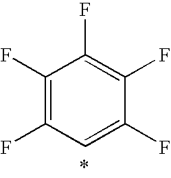 |
 |
 |
 |
 |
 |
 |
|
|
|
|
 |
|
 |
|
 |
| Monovalent | ||
| Ring Structure | Name | Heteroaryl Residue |
|
|
pyridine | pyridyl |
|
|
pyrimidine | pyrimidyl |
|
|
pyridazine | pyridazyl |
|
|
pyrazine | pyrazyl |
|
|
thiophene | thienyl |
|
|
benzothiophene | benzothienyl |
|
|
pyrrol | pyrryl |
|
|
furane | furyl |
|
|
benzofurane | benzofuryl, |
 |
indole | indolyl |
 |
carbazole | carbazolyl |
 |
benzotriazole | benzotriazolyl |
|
|
tetrazole | tetrazolyl |
|
|
thiazole | thiazolyl |
-
- which are bonded via a carbon ring atom,
- or a moiety selected from the following moieties (bonded preferably via one of the carbon atoms labelled with an asterisk):


thienothienyl
dithiaindacenyl

chinolyl

isochinolyl

chinoxalyl

acridyl
wherein Q has one of its meanings other than hydrogen
benzo[1,2-d;4,5-d′]bisthiazolyl

carbazolyl wherein Q has one of its meanings other than H;

dibenzothiophenyl

wherein Q has one of its meanings other than hydrogen;
thiazolo[5,4-d]thiazolyl
as well as phenanthrolyl, triazinyl, thienyl, pyrazolyl, imidazolyl, or
thia- and oxadiazolyl

wherein each Y, independently of the other, is ethynyl substituted by halo-substituted hydrocarbyl with up to 40 carbon atoms or by heteroaryl;

wherein Y* and Y** are ethynyl independently of each other substituted with unsubstituted or substituted hydrocarbyl with up to 40 carbon atoms, unsubstituted or substituted hydrocarbyloxy with up to 40 carbon atoms, hydrocarbylthio with up to 40 carbon atoms, unsubstituted or substituted heteroaryl, unsubstituted or substituted heteroaryloxy, unsubstituted or substituted heteroarylthio, cyano, carbamoyl, wherein Hal represents a halogen atom, substituted amino, halo-C1-C8-alkyl, such as trifluoromethyl, halo, or substituted silyl, while the rings or ring systems labelled A and B and the symbols X, Y, n, m and p have the meanings defined for a compound of the formula IA.

by reacting it with compounds of the formulae IV
Y***—H (IV)
wherein Y*** is Y* and Y** as defined for a compound of the formula II, in the presence of a strong base sufficient for removal of the acetylenic proton, such as a Grignard reagent, an alkali-metal alcoholate, such as potassium t-butoxide, a lithium amide such as lithium diisopropylamide, or the like in an appropriate solvent, such as tetrahydrofurane, dioxane, diethoxymethane or dimethoxymethane, glyme, diglyme, toluene or anisol or mixtures of two or more thereof, e.g. at temperatures in the range from 0 to 100° C., preferably from 10 to 80° C.
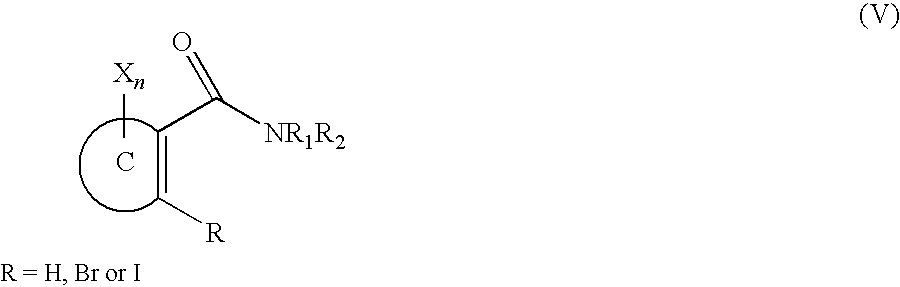
wherein ring C, X and n are as defined for a compound of the formula I and R1 and R2 are independently of the other C1-C8-alkyl or R1 is C1-C8 alkyl and R2 is lower alkoxy such as methoxy or ethoxy (Weinreb amide), in the presence of a lithiating agent such as n-butyllithium or LDA, in an appropriate solvent, e.g. diethyl ether, THF or a hydrocarbon, such as C1-C8-alkanes or also mixtures of two or more of these solvents, preferably at lower temperatures, e.g. in the range from −100 to 50° C., e.g. from −80 to 30° C., which leads under dimerisation to a compound of formula III with C2h symmetry.

wherein ring BC′ is a ring completing ring or ring system C and ring or ring system B in a compound of the formula III and X and n are as defined for a compound of the formula I, with a compound of the formula VIII,

under aldol condensation conditions to give a compound or—where it applies—a mixture (which can then be separated according to standard procedures to give the corresponding isomerically pure compound) of compounds of the following formula IIIA which falls under formula III (wherein Z=X and p=n in formula III):

wherein BC′ is a ring or ring system completing ring systems B and C (meaning forming together with the annealed benzo ring a ring system B or C) in a compound of the formula III and X and n are as defined for a compound of the formula I.

can be used which may be unsubstituted or substituted by X and Z if n and/or p is 1 or more.

wherein B′ is a ring or ring system B as defined under formula I and Z and p are as defined for a compound of the formula I, e.g. under aldol condensation conditions to give a compound or—where it applies—a mixture of compounds (which can then be separated according to standard procedures to give the corresponding isomerically pure compound) of the following formula IIIA which falls under formula III:

wherein ring or ring system BC′ is a ring completing ring or ring system C in a compound of the formula III, ring or ring system B is as defined for a compound of the formula I and X, Z, p and n are as defined for a compound of the formula I.


where Y***—H is a compound of the formula IV as defined above, B′ and C′ are rings complementing a di- or polycyclic ring B and C in a corresponding compound of the formula I, respectively, and X, Z, n and p are as defined for a compound of the formula I, respectively.

by reaction with a compound of the formula XIV,
X/Z—C≡C—H (XIV)
wherein X/Z—C≡C corresponds to X and Z in a compound of the formula I* or I**, e.g. in the presence of a strong base sufficient for removal of the acetylenic proton, such as a Grignard reagent, an alkali-metal alcoholate, such as potassium tert-butoxide, a lithium amide such as lithium isopropylamide, or the like, e.g. in an appropriate solvent, such as tetrahydrofurane, dioxane, diethoxymethane or dimethoxymethane, glyme, diglyme, toluene or anisol or mixtures of two or more thereof, e.g. at temperatures in the range from 0 to 100° C., preferably from 10 to 80° C.
-
- a) by reacting a 9,10-dibromoanthracene compound of the formula XXII,

wherein X, Z, n and p are as defined for a compound of the formula XXI, or a substituted derivative thereof carrying, preferably in the presence of an appropriate solvent, e.g. a hydrocarbon, such as toluene, and a tertiary nitrogen base, e.g. triethyl-amine, at preferred temperatures in the range from 0° C. to the reflux temperature of the reaction mixture, with an ethynyl compound of the formula XXIII
Ya—C≡C—H (XXIII)
wherein Ya is fluoro- or chloro-substituted hydrocarbyl, under Sonogashira coupling conditions or the like, e.g. in the presence of palladium(II)acetate, triphenylphosphine and copper iodide; or
-
- b) by reacting a compound of the formula XXIV,
Ya*—C≡C—H (XXIV)
wherein Ya* is halo(especially bromo or iodo)-substituted hydrocarbyl, preferably in the presence of an appropriate solvent, such as an ether, e.g. tetrahydrofurane, and/or hydro-carbons, such as hexanes, with a strong base sufficient for removal of the acetylenic proton, such as a Grignard reagent, an alkali-metal alcoholate, such as potassium t-butoxide, a lithium amide, such as lithium diisopropylamide, or the like, to the corresponding deprotonated compound (acetylide), e.g. at temperatures from −90 to 25° C., then reacting the resulting mixture comprising the acetylide with an anthraquinone of the formula XXV,
- b) by reacting a compound of the formula XXIV,

e.g. at temperatures in the range from 0 to 50° C., and reducing resulting diol compound, e.g. with tin(II)-chloride in a mixture of a ketone, e.g. acetone, water and an acid, such as hydrochloric or acetic acid, e.g. at temperatures in the range from 0 to 50° C., to give a compound of the formula XXI.


| TABLE 1 |
| Performance of OFET from Example 7 material |
| Charge Carrier | Threshold | Sub-Thres- | ||
| Gate | Mobility | Voltage | hold Slope | On/Off |
| dielectric | (cm2/Vs) | (V) | (V/decade) | Ratio |
| SiO2 | 4*10−4 | −12.3 | 0.9 | 9.9*106 |
Claims (18)


Applications Claiming Priority (4)
| Application Number | Priority Date | Filing Date | Title |
|---|---|---|---|
| EP05111963.4 | 2005-12-12 | ||
| EP05111963 | 2005-12-12 | ||
| EP05111963 | 2005-12-12 | ||
| PCT/EP2006/069281 WO2007068618A1 (en) | 2005-12-12 | 2006-12-04 | Organic semiconductors and their manufacture |
Publications (2)
| Publication Number | Publication Date |
|---|---|
| US20090299070A1 US20090299070A1 (en) | 2009-12-03 |
| US8101776B2 true US8101776B2 (en) | 2012-01-24 |
Family
ID=36123034
Family Applications (1)
| Application Number | Title | Priority Date | Filing Date |
|---|---|---|---|
| US12/086,157 Active 2028-10-11 US8101776B2 (en) | 2005-12-12 | 2006-12-04 | Organic semiconductors and their manufacture |
Country Status (6)
| Country | Link |
|---|---|
| US (1) | US8101776B2 (en) |
| EP (2) | EP2573833B1 (en) |
| JP (1) | JP5410760B2 (en) |
| CN (1) | CN101356662B (en) |
| TW (1) | TWI415317B (en) |
| WO (1) | WO2007068618A1 (en) |
Cited By (13)
| Publication number | Priority date | Publication date | Assignee | Title |
|---|---|---|---|---|
| US20100117066A1 (en) * | 2007-04-28 | 2010-05-13 | Merck Patent Gmbh | Organic Semiconductors |
| US20120273770A1 (en) * | 2009-12-14 | 2012-11-01 | Idemitsu Kosan Co., Ltd. | Polycyclic ring-fused compound and organic thin film transistor utilizing same |
| US8821762B2 (en) | 2008-12-18 | 2014-09-02 | Merck Patent Gmbh | Anthra[2,3-b]benzo[d]thiophene derivatives and their use as organic semiconductors |
| US9067886B2 (en) | 2011-11-22 | 2015-06-30 | Polyera Corporation | Compounds having semiconducting properties and related compositions and devices |
| US10050201B2 (en) | 2010-04-19 | 2018-08-14 | Merck Patent Gmbh | Polymers of benzodithiophene and their use as organic semiconductors |
| US10954391B2 (en) | 2013-08-22 | 2021-03-23 | Sony Corporation | Water soluble fluorescent or colored dyes and methods for their use |
| US10989715B2 (en) | 2016-04-06 | 2021-04-27 | Sony Corporation | Ultra bright dimeric or polymeric dyes with spacing linker groups |
| US11312736B1 (en) | 2017-10-05 | 2022-04-26 | Sony Corporation | Programmable polymeric drugs |
| US11352502B2 (en) | 2019-09-26 | 2022-06-07 | Sony Group Corporation | Polymeric tandem dyes with linker groups |
| US11377563B2 (en) | 2016-06-06 | 2022-07-05 | Sony Corporation | Ionic polymers comprising fluorescent or colored reporter groups |
| US11453783B2 (en) | 2018-03-21 | 2022-09-27 | Sony Corporation | Polymeric tandem dyes with linker groups |
| US11874280B2 (en) | 2018-03-19 | 2024-01-16 | Sony Group Corporation | Use of divalent metals for enhancement of fluorescent signals |
| US11931419B2 (en) | 2017-11-16 | 2024-03-19 | Sony Group Corporation | Programmable polymeric drugs |
Families Citing this family (36)
| Publication number | Priority date | Publication date | Assignee | Title |
|---|---|---|---|---|
| EP2067782B2 (en) † | 2006-08-28 | 2018-06-27 | Tosoh Corporation | Heteroacene derivative, tetrahaloterphenyl derivative, and their production methods |
| JP5272345B2 (en) * | 2006-08-28 | 2013-08-28 | 東ソー株式会社 | Heteroacene derivatives, tetrahaloterphenyl derivatives and methods for producing them |
| US8217389B2 (en) | 2006-10-12 | 2012-07-10 | Idemitsu Kosan, Co., Ltd. | Organic thin film transistor device and organic thin film light-emitting transistor |
| JP5160842B2 (en) * | 2007-08-28 | 2013-03-13 | 山本化成株式会社 | Organic transistor |
| WO2009125705A1 (en) * | 2008-04-10 | 2009-10-15 | 出光興産株式会社 | Compound for organic thin-film transistor and organic thin-film transistor using the compound |
| TWI471328B (en) * | 2008-07-02 | 2015-02-01 | Basf Se | High performance solution processable seminconductor based on dithieno [2,3-d:2',3'-d']benzo[1,2-b:4,5-b'] dithiophene |
| US8154013B2 (en) | 2008-11-19 | 2012-04-10 | Xerox Corporation | Organic thin-film transistors |
| GB2465626B (en) * | 2008-11-28 | 2013-07-31 | Cambridge Display Tech Ltd | Organic semiconductors |
| SG173794A1 (en) * | 2009-02-20 | 2011-09-29 | Agency Science Tech & Res | Planar conjugated compounds and their applications for organic electronics |
| CN102448945B (en) | 2009-05-29 | 2016-01-20 | 出光兴产株式会社 | Anthracene derivative and organic electroluminescent element using the same |
| GB2472413B (en) | 2009-08-05 | 2014-04-23 | Cambridge Display Tech Ltd | Organic semiconductors |
| GB2479793A (en) | 2010-04-23 | 2011-10-26 | Cambridge Display Tech Ltd | Organic semiconductor compounds and devices |
| KR101088935B1 (en) | 2010-05-31 | 2011-12-01 | 한남대학교 산학협력단 | Synthesis of a novel anthracene derivative for organic thin-film transistors |
| JP5811542B2 (en) * | 2010-06-15 | 2015-11-11 | 株式会社リコー | Organic semiconductor material precursor comprising dithienobenzodithiophene derivative, ink, insulating member, and method for producing charge transporting member |
| WO2012013508A1 (en) | 2010-07-30 | 2012-02-02 | Basf Se | Amphiphilic protein in printed electronics |
| US9306172B2 (en) * | 2010-08-13 | 2016-04-05 | Merck Patent Gmbh | Anthra[2,3-b:7,6-b']dithiophene derivatives and their use as organic semiconductors |
| JP5891646B2 (en) * | 2011-08-11 | 2016-03-23 | 株式会社リコー | Novel organic semiconductor material and electronic device using the same |
| KR101507002B1 (en) * | 2011-12-30 | 2015-03-31 | 제일모직 주식회사 | Compound for organic optoelectronic device, organic light emitting diode including the same and display including the organic light emitting diode |
| KR101982746B1 (en) * | 2012-06-27 | 2019-05-28 | 덕산네오룩스 주식회사 | Compound for organic electronic element, organic electronic element using the same, and a electronic device thereof |
| JP5896935B2 (en) | 2012-08-27 | 2016-03-30 | 富士フイルム株式会社 | Organic thin film transistor, organic semiconductor thin film and organic semiconductor material |
| JP6008158B2 (en) | 2013-03-05 | 2016-10-19 | Jnc株式会社 | Chalcogen-containing organic compounds and uses thereof |
| DE102013110693B4 (en) | 2013-09-27 | 2024-04-25 | Heliatek Gmbh | Photoactive organic material for optoelectronic components |
| WO2015109136A2 (en) * | 2014-01-16 | 2015-07-23 | Sony Corporation | Water soluble fluorescent or colored dyes and methods for their use |
| WO2016031707A1 (en) * | 2014-08-26 | 2016-03-03 | 富士フイルム株式会社 | Organic semiconductor device, method of manufacturing same, and topochemical polymerizable organic semiconductor compound |
| CN107454903B (en) | 2015-02-26 | 2021-01-01 | 索尼公司 | Water-soluble fluorescent or colored dyes containing conjugated groups |
| EP3262022A4 (en) * | 2015-02-26 | 2018-08-15 | Sony Corporation | Phenylethynylnaphthalene dyes and methods for their use |
| JP6708447B2 (en) * | 2015-03-10 | 2020-06-10 | 学校法人関西学院 | Rubrene derivative and method for producing the same |
| US10865310B2 (en) | 2015-05-11 | 2020-12-15 | Sony Corporation Of America | Ultra bright dimeric or polymeric dyes |
| CA3018564A1 (en) | 2016-04-01 | 2017-10-05 | Sony Corporation | Ultra bright dimeric or polymeric fluorescent and colored dyes |
| US11434377B2 (en) | 2016-04-01 | 2022-09-06 | Sony Corporation | Ultra bright dimeric or polymeric dyes with rigid spacing groups |
| JP2019519490A (en) | 2016-05-10 | 2019-07-11 | ソニー株式会社 | Ultra bright polymer dye having a peptide backbone |
| JP7068192B2 (en) | 2016-05-10 | 2022-05-16 | ソニーグループ株式会社 | Compositions containing polymer dyes and cyclodextrins, and their use |
| CN109071961B (en) | 2016-05-11 | 2021-04-27 | 索尼公司 | Ultra-bright dimeric or polymeric dyes |
| WO2019170481A1 (en) | 2018-03-07 | 2019-09-12 | Basf Se | Patterning method for preparing top-gate, bottom-contact organic field effect transistors |
| KR102341687B1 (en) | 2018-03-08 | 2021-12-21 | 주식회사 클랩 | Organic Field Effect Transistors Including Semiconducting Single Walled Carbon Nanotubes and Organic Semiconducting Materials |
| KR102457044B1 (en) | 2018-06-26 | 2022-10-21 | 주식회사 클랩 | Vinyl ether polymer as dielectric |
Citations (10)
| Publication number | Priority date | Publication date | Assignee | Title |
|---|---|---|---|---|
| US6252245B1 (en) | 1999-03-29 | 2001-06-26 | Howard Edan Katz | Device comprising n-channel semiconductor material |
| US20020164835A1 (en) | 2001-05-04 | 2002-11-07 | Dimitrakopoulos Christos Dimitrios | Organic n-channel semiconductor device of N,N' 3,4,9,10 perylene tetracarboxylic diimide |
| US20030105365A1 (en) | 2001-09-27 | 2003-06-05 | 3M Innovative Properties Company | Substituted pentacene semiconductors |
| US20030144526A1 (en) | 1996-07-08 | 2003-07-31 | Nps Pharmaceuticals, Inc. | Calcium receptor-active compounds |
| US6690029B1 (en) | 2001-08-24 | 2004-02-10 | University Of Kentucky Research Foundation | Substituted pentacenes and electronic devices made with substituted pentacenes |
| EP1416069A1 (en) | 2001-08-09 | 2004-05-06 | Asahi Kasei Kabushiki Kaisha | Organic semiconductor element |
| WO2005055248A2 (en) | 2003-11-28 | 2005-06-16 | Merck Patent Gmbh | Organic semiconducting layer formulations comprising polyacenes and organic binder polymers |
| WO2005073338A2 (en) | 2003-12-04 | 2005-08-11 | Massachusetts Institute Of Technology | Fluorescent, semi-conductive polymers, and devices comprising them |
| WO2006059486A1 (en) | 2004-12-02 | 2006-06-08 | Konica Minolta Holdings, Inc. | Organic thin-film transistor material, organic thin-film transistor, field effect transistor, switching device, organic semiconductor material, and organic semiconductor film |
| US20060220007A1 (en) | 2005-04-05 | 2006-10-05 | Bailey David B | Acene compounds having a single terminal fused thiophene as semiconductor materials for thin film transistors and methods of making the same |
Family Cites Families (6)
| Publication number | Priority date | Publication date | Assignee | Title |
|---|---|---|---|---|
| DE2320528A1 (en) | 1973-04-21 | 1974-11-07 | Hoechst Ag | PROCESS FOR THE PRODUCTION OF ACETYLENES |
| FR2664430B1 (en) | 1990-07-04 | 1992-09-18 | Centre Nat Rech Scient | THIN FILM FIELD EFFECT TRANSISTOR WITH MIS STRUCTURE, IN WHICH THE INSULATION AND THE SEMICONDUCTOR ARE MADE OF ORGANIC MATERIALS. |
| JP2801078B2 (en) * | 1990-10-29 | 1998-09-21 | 山本化成株式会社 | Method for producing acetylene derivative |
| US6265243B1 (en) | 1999-03-29 | 2001-07-24 | Lucent Technologies Inc. | Process for fabricating organic circuits |
| JP2002275384A (en) * | 2001-03-16 | 2002-09-25 | Japan Science & Technology Corp | Photoresponsive pigment for laser |
| JP2007088222A (en) * | 2005-09-22 | 2007-04-05 | Konica Minolta Holdings Inc | Organic semiconductor material, organic semiconductor film, organic semiconductor device, and organic thin-film transistor |
-
2006
- 2006-12-04 US US12/086,157 patent/US8101776B2/en active Active
- 2006-12-04 EP EP12198120.3A patent/EP2573833B1/en active Active
- 2006-12-04 JP JP2008544954A patent/JP5410760B2/en active Active
- 2006-12-04 WO PCT/EP2006/069281 patent/WO2007068618A1/en active Application Filing
- 2006-12-04 EP EP06830339A patent/EP1961052B1/en active Active
- 2006-12-04 CN CN200680046536.0A patent/CN101356662B/en active Active
- 2006-12-11 TW TW095146196A patent/TWI415317B/en active
Patent Citations (10)
| Publication number | Priority date | Publication date | Assignee | Title |
|---|---|---|---|---|
| US20030144526A1 (en) | 1996-07-08 | 2003-07-31 | Nps Pharmaceuticals, Inc. | Calcium receptor-active compounds |
| US6252245B1 (en) | 1999-03-29 | 2001-06-26 | Howard Edan Katz | Device comprising n-channel semiconductor material |
| US20020164835A1 (en) | 2001-05-04 | 2002-11-07 | Dimitrakopoulos Christos Dimitrios | Organic n-channel semiconductor device of N,N' 3,4,9,10 perylene tetracarboxylic diimide |
| EP1416069A1 (en) | 2001-08-09 | 2004-05-06 | Asahi Kasei Kabushiki Kaisha | Organic semiconductor element |
| US6690029B1 (en) | 2001-08-24 | 2004-02-10 | University Of Kentucky Research Foundation | Substituted pentacenes and electronic devices made with substituted pentacenes |
| US20030105365A1 (en) | 2001-09-27 | 2003-06-05 | 3M Innovative Properties Company | Substituted pentacene semiconductors |
| WO2005055248A2 (en) | 2003-11-28 | 2005-06-16 | Merck Patent Gmbh | Organic semiconducting layer formulations comprising polyacenes and organic binder polymers |
| WO2005073338A2 (en) | 2003-12-04 | 2005-08-11 | Massachusetts Institute Of Technology | Fluorescent, semi-conductive polymers, and devices comprising them |
| WO2006059486A1 (en) | 2004-12-02 | 2006-06-08 | Konica Minolta Holdings, Inc. | Organic thin-film transistor material, organic thin-film transistor, field effect transistor, switching device, organic semiconductor material, and organic semiconductor film |
| US20060220007A1 (en) | 2005-04-05 | 2006-10-05 | Bailey David B | Acene compounds having a single terminal fused thiophene as semiconductor materials for thin film transistors and methods of making the same |
Non-Patent Citations (9)
| Title |
|---|
| B. Li et al., Dyes and Pigments, vol. 62, No. 3, (Sep. 2004), pp. 299-304. |
| C. Sheraw et al., Adv. Mater., vol. 15 No. 23, Dec. 3, 2003, pp. 2009-2011. |
| King, Med Principle and Practice, (1994), pp. 206-208. * |
| M. Payne et al., Organic Letters, vol. 6, No. 10 (2004), pp. 1609-1612. |
| M. Payne et al., Organic Letters, vol. 6, No. 19, (2004), pp. 3325-3328. |
| P. Lane et al., Proceedings of SPIE-The International Society for Optical Engineering; Organic Light-Emitting Materials and Devices IX, vol. 5937, (Oct. 9, 2005), pp. 1-10. |
| P. Lane et al., Proceedings of SPIE—The International Society for Optical Engineering; Organic Light-Emitting Materials and Devices IX, vol. 5937, (Oct. 9, 2005), pp. 1-10. |
| Patent Abstracts of Japan Publication No. 04164037, Jun. 9, 1992. |
| Patent Abstracts of Japan Publication No. 2002275384, Sep. 25, 2002. |
Cited By (18)
| Publication number | Priority date | Publication date | Assignee | Title |
|---|---|---|---|---|
| US20100117066A1 (en) * | 2007-04-28 | 2010-05-13 | Merck Patent Gmbh | Organic Semiconductors |
| US8821762B2 (en) | 2008-12-18 | 2014-09-02 | Merck Patent Gmbh | Anthra[2,3-b]benzo[d]thiophene derivatives and their use as organic semiconductors |
| US20120273770A1 (en) * | 2009-12-14 | 2012-11-01 | Idemitsu Kosan Co., Ltd. | Polycyclic ring-fused compound and organic thin film transistor utilizing same |
| US8946688B2 (en) * | 2009-12-14 | 2015-02-03 | Idemitsu Kosan Co., Ltd. | Polycyclic ring-fused compound and organic thin film transistor utilizing the same |
| US10050201B2 (en) | 2010-04-19 | 2018-08-14 | Merck Patent Gmbh | Polymers of benzodithiophene and their use as organic semiconductors |
| US10158079B2 (en) | 2010-04-19 | 2018-12-18 | Merck Patent Gmbh | Polymers of benzodithiophene and their use as organic semiconductors |
| US9067886B2 (en) | 2011-11-22 | 2015-06-30 | Polyera Corporation | Compounds having semiconducting properties and related compositions and devices |
| US11434374B2 (en) | 2013-08-22 | 2022-09-06 | Sony Corporation | Water soluble fluorescent or colored dyes and methods for their use |
| US10954391B2 (en) | 2013-08-22 | 2021-03-23 | Sony Corporation | Water soluble fluorescent or colored dyes and methods for their use |
| US11939474B2 (en) | 2013-08-22 | 2024-03-26 | Sony Group Corporation | Water soluble fluorescent or colored dyes and methods for their use |
| US10989715B2 (en) | 2016-04-06 | 2021-04-27 | Sony Corporation | Ultra bright dimeric or polymeric dyes with spacing linker groups |
| US11377563B2 (en) | 2016-06-06 | 2022-07-05 | Sony Corporation | Ionic polymers comprising fluorescent or colored reporter groups |
| US11312736B1 (en) | 2017-10-05 | 2022-04-26 | Sony Corporation | Programmable polymeric drugs |
| US11931419B2 (en) | 2017-11-16 | 2024-03-19 | Sony Group Corporation | Programmable polymeric drugs |
| US11874280B2 (en) | 2018-03-19 | 2024-01-16 | Sony Group Corporation | Use of divalent metals for enhancement of fluorescent signals |
| US11453783B2 (en) | 2018-03-21 | 2022-09-27 | Sony Corporation | Polymeric tandem dyes with linker groups |
| US11352502B2 (en) | 2019-09-26 | 2022-06-07 | Sony Group Corporation | Polymeric tandem dyes with linker groups |
| US11945955B2 (en) | 2019-09-26 | 2024-04-02 | Sony Group Corporation | Polymeric tandem dyes with linker groups |
Also Published As
| Publication number | Publication date |
|---|---|
| CN101356662B (en) | 2014-08-06 |
| US20090299070A1 (en) | 2009-12-03 |
| JP2009519595A (en) | 2009-05-14 |
| EP1961052A1 (en) | 2008-08-27 |
| EP2573833A1 (en) | 2013-03-27 |
| EP2573833B1 (en) | 2014-04-02 |
| EP1961052B1 (en) | 2013-03-06 |
| TWI415317B (en) | 2013-11-11 |
| JP5410760B2 (en) | 2014-02-05 |
| TW200737559A (en) | 2007-10-01 |
| WO2007068618A1 (en) | 2007-06-21 |
| CN101356662A (en) | 2009-01-28 |
Similar Documents
| Publication | Publication Date | Title |
|---|---|---|
| US8101776B2 (en) | Organic semiconductors and their manufacture | |
| US9911927B2 (en) | Compounds having semiconducting properties and related compositions and devices | |
| US7385221B1 (en) | Silylethynylated heteroacenes and electronic devices made therewith | |
| US6864396B2 (en) | Substituted pentacene semiconductors | |
| US7528176B2 (en) | Carbonyl-functionalized thiophene compounds and related device structures | |
| KR102079230B1 (en) | Fused Polycyclic Heteroaromatic Compound, Organic Thin Film Including Compound and Electronic Device Including Organic Thin Film | |
| KR102043985B1 (en) | Fused Polyheteroaromatic Compound, Organic Thin Film Including the Compound and Electronic Device Including the Organic Thin Film | |
| EP2132213A1 (en) | Silylethynylated heteroacenes and electronic devices made therewith | |
| US20060220007A1 (en) | Acene compounds having a single terminal fused thiophene as semiconductor materials for thin film transistors and methods of making the same | |
| JP5580848B2 (en) | Azaperylenes as organic semiconductors | |
| US8471019B2 (en) | Quinoid systems as organic semiconductors | |
| US9444058B2 (en) | Preparation of pi-extended naphthalene diimides and their use as semiconductor | |
| Anant et al. | Synthesis and characterization of pyrene-centered oligothiophenes | |
| US20200168806A1 (en) | Compound and organic thin film and thin film transistor and electronic device | |
| Castrillo | Preparation and characterization of p-type organic thin film transistors based on a novel triindole derivative | |
| Yang | Development of π-Extended Heteroacene-based Materials toward Application in Organic Field-Effect Transistors | |
| GB2542563A (en) | Pentacene derivatives with C-alkyne solubilising units and their applications as small molecule organic semiconductors |
Legal Events
| Date | Code | Title | Description |
|---|---|---|---|
| AS | Assignment |
Owner name: CIBA CORP., NEW YORK Free format text: ASSIGNMENT OF ASSIGNORS INTEREST;ASSIGNORS:BERENS, ULRICH;BIENEWALD, FRANK;KIRNER, HANS JUERG;SIGNING DATES FROM 20080515 TO 20080519;REEL/FRAME:023135/0447 |
|
| AS | Assignment |
Owner name: BASF SE, GERMANY Free format text: ASSET TRANSFER AGREEMENT;ASSIGNOR:CIBA CORPORATION;REEL/FRAME:027366/0411 Effective date: 20090702 |
|
| STCF | Information on status: patent grant |
Free format text: PATENTED CASE |
|
| FPAY | Fee payment |
Year of fee payment: 4 |
|
| MAFP | Maintenance fee payment |
Free format text: PAYMENT OF MAINTENANCE FEE, 8TH YEAR, LARGE ENTITY (ORIGINAL EVENT CODE: M1552); ENTITY STATUS OF PATENT OWNER: LARGE ENTITY Year of fee payment: 8 |
|
| AS | Assignment |
Owner name: CLAP CO., LTD., KOREA, REPUBLIC OF Free format text: ASSIGNMENT OF ASSIGNORS INTEREST;ASSIGNOR:BASF SE;REEL/FRAME:052459/0201 Effective date: 20200121 |
|
| FEPP | Fee payment procedure |
Free format text: ENTITY STATUS SET TO SMALL (ORIGINAL EVENT CODE: SMAL); ENTITY STATUS OF PATENT OWNER: SMALL ENTITY |
|
| MAFP | Maintenance fee payment |
Free format text: PAYMENT OF MAINTENANCE FEE, 12TH YR, SMALL ENTITY (ORIGINAL EVENT CODE: M2553); ENTITY STATUS OF PATENT OWNER: SMALL ENTITY Year of fee payment: 12 |