WO2005101037A1 - 電子部品の高周波電気特性測定方法および装置 - Google Patents
電子部品の高周波電気特性測定方法および装置 Download PDFInfo
- Publication number
- WO2005101037A1 WO2005101037A1 PCT/JP2004/004882 JP2004004882W WO2005101037A1 WO 2005101037 A1 WO2005101037 A1 WO 2005101037A1 JP 2004004882 W JP2004004882 W JP 2004004882W WO 2005101037 A1 WO2005101037 A1 WO 2005101037A1
- Authority
- WO
- WIPO (PCT)
- Prior art keywords
- measurement
- measured
- measuring
- electronic component
- transmission line
- Prior art date
- Legal status (The legal status is an assumption and is not a legal conclusion. Google has not performed a legal analysis and makes no representation as to the accuracy of the status listed.)
- Ceased
Links
Classifications
-
- G—PHYSICS
- G01—MEASURING; TESTING
- G01R—MEASURING ELECTRIC VARIABLES; MEASURING MAGNETIC VARIABLES
- G01R35/00—Testing or calibrating of apparatus covered by the other groups of this subclass
- G01R35/005—Calibrating; Standards or reference devices, e.g. voltage or resistance standards, "golden" references
-
- G—PHYSICS
- G01—MEASURING; TESTING
- G01R—MEASURING ELECTRIC VARIABLES; MEASURING MAGNETIC VARIABLES
- G01R27/00—Arrangements for measuring resistance, reactance, impedance, or electric characteristics derived therefrom
- G01R27/28—Measuring attenuation, gain, phase shift or derived characteristics of electric four pole networks, i.e. two-port networks; Measuring transient response
- G01R27/32—Measuring attenuation, gain, phase shift or derived characteristics of electric four pole networks, i.e. two-port networks; Measuring transient response in circuits having distributed constants, e.g. having very long conductors or involving high frequencies
-
- G—PHYSICS
- G01—MEASURING; TESTING
- G01R—MEASURING ELECTRIC VARIABLES; MEASURING MAGNETIC VARIABLES
- G01R31/00—Arrangements for testing electric properties; Arrangements for locating electric faults; Arrangements for electrical testing characterised by what is being tested not provided for elsewhere
- G01R31/28—Testing of electronic circuits, e.g. by signal tracer
- G01R31/282—Testing of electronic circuits specially adapted for particular applications not provided for elsewhere
- G01R31/2822—Testing of electronic circuits specially adapted for particular applications not provided for elsewhere of microwave or radiofrequency circuits
Definitions
- the present invention relates to a method for measuring high-frequency electrical characteristics of electronic components such as filters, power plugs, and parans, or impedance elements such as chip inductors and chip capacitors.
- the present invention relates to a method for correcting a measurement error when measuring a scattering coefficient or an impedance value of the electronic component by a measuring device.
- TRL Through-reflection-load correction and SOLT (short-open-load-throw) correction
- Figures la and 1b show the measurement system using a network analyzer and the error models used in the SOLT and TRL corrections.
- the electronic component 1 as a subject is connected to a transmission path formed on the upper surface of the measuring jig 2. Both ends of the transmission path of the measuring jig 2 are connected via coaxial cables 3 to measuring ports of a network analyzer (not shown).
- S 1 1A ⁇ S 22A scattering coefficient of the object e. O ⁇ eu scattering coefficient of one measurement port side
- f 00 ⁇ f 1 1 is the scattering coefficient of the other measurement port side.
- measurement must be performed by attaching at least three types of devices (standard devices) with known scattering coefficients to the surface to be measured.
- SOLT correction For SOLT correction, as shown in Figure 2,
- the TRL correction is a transmission line 5a in a directly connected state (Through), a transmission line 5b in total reflection (Reflection is normally short-circuited), instead of a standard device with a device shape that is difficult to realize.
- a transmission line 5b in total reflection Reflection is normally short-circuited
- Lines 5c and 5d having different lengths are used as standards.
- the transmission lines 5a to 5d can be easily manufactured with a relatively known scattering coefficient, and if total reflection is short-circuited, their characteristics can be predicted relatively easily. It was done. Therefore, in principle, the characteristics of the subject 1 alone can be measured.
- the through transmission line 5a is a so-called Zero-through.
- the subject is connected in series to a measuring jig 5e, which is longer than the through transmission path 5a by the size of the subject, and measured.
- a measuring jig 5e which is longer than the through transmission path 5a by the size of the subject, and measured.
- Japanese Patent Laying-Open No. 6-34686 discloses a method for calibrating a network analyzer having two test terminals connected to a subject via a strip line. That is, in the first calibration measurement, transmission and reflection parameters are measured on a line whose propagation constant is unknown, on a strip line connected in a non-reflective manner between the two test terminals, and the same line is measured. Three additional calibration measurements using the three calibration standards implemented by the reflective symmetric and reciprocal discontinuities introduced at the three different locations on the track. .
- an object of the present invention is to solve the problems in TRL correction and SOLT correction and to provide a high-precision method for measuring high-frequency electrical characteristics of electronic components that is not affected by variations in characteristics of connection parts. .
- Another object of the present invention is to provide a high-precision electronic device for measuring high-frequency electrical characteristics of electronic components. Disclosure of the invention
- the invention according to claim 1 is a method for measuring high-frequency electrical characteristics of an electronic component, comprising: a plurality of signal conductors spaced apart from each other; and at least one ground conductor. Preparing a transmission line having a known electrical characteristic per unit length, connecting each of the signal conductors and the ground conductor to a measurement port of a measuring instrument, and a length direction of each of the signal conductors.
- a method for measuring high-frequency electrical characteristics of electronic components characterized by the following.
- a subject is connected in series between a signal conductor and a ground conductor of a transmission line, which is a measuring jig, or is connected between a signal conductor and a ground conductor, and its reflection and transfer coefficient are measured.
- this method of measuring electrical characteristics such as impedance values and quality factors, it is a method to remove errors in transmission lines and other measurement systems.
- the present invention when measuring an error of a measurement system, it is easy to manufacture a transmission line having a known physical true value as an electrical characteristic, and a transmission line having a good total reflection (short circuit) state can be easily obtained. It is based on the knowledge that it can be realized.
- At least three points on a transmission line having a plurality of signal conductors having uniform electrical characteristics in the length direction are set to a total reflection state to identify an error factor of the measurement system.
- a total reflection state for example, a short tip or a knife edge is shunt-connected, and the signal conductor and the ground conductor of the transmission line are short-circuited.
- the signal conductors are put into a through state mutually, and an error factor of the measurement system is identified.
- a through state for example, a series connection of through chips with no directivity in the transfer coefficient is used.
- R R R R R Neinamasa the principle of the correction according to the present invention
- the transmission line used as a measurement jig must have known electrical characteristics per unit length.
- the loss per unit length, electrical length, and characteristic impedance must be known. These can be predicted by simulation, or several types of transmission lines with the same structure can be manufactured using substrates of the same material, and can be estimated from the measured results of the electrical characteristics.
- a planar transmission line having a known electric characteristic per unit length can be easily realized by using, for example, a known printed circuit board manufacturing technique.
- the short chip refers to a general part in an electrically shorted state, and is not limited to a chip part but may be a metal piece or a tool.
- the contact length in the length direction of the transmission path such as a knife edge is short.
- the reflection coefficient will be a value of -1.
- the inductance value must be known. Normally, in the microwave band, near-ideal conditions can be obtained relatively easily compared to open conditions. When high measurement accuracy is required, the inductance of the short chip may be obtained by a simple simulation or the like.
- R R R R R measurement that can be measured by the series method, it is necessary to connect through the ports. At this time, the characteristics of the through chip do not need to be known. For example, a chip resistor whose resistance value is unknown may be used, but the directionality must not be present. Except for an isolator and a circulator (a special element that uses a magnetic substance under a DC magnetic field) or an active element such as a semiconductor amplifier, a device that has directionality in signal transmission cannot be made (reciprocity theorem). This assumption is virtually automatically satisfied.
- a through chip is not limited to a chip component, but can be any component as long as it has no direction in signal transmission.
- the standard devices to be measured are all the same short chip 10, which is measured at three or more locations on the transmission line 12 formed in the measurement jig 11 as shown in FIG.
- the correction on the port 1 (connector 11a) side will be described, but the same operation is required on the port 2 (connector lib) side.
- the coplanar wave guide is composed of two signal conductors 12a and 12b arranged on a straight line, one end of which is spaced apart, and the other end of which is connected to connectors 11a and 11b, respectively.
- Ground conductors 12c are arranged on both sides in the width direction of the signal conductors 12a and 12b, and the signal conductors 12a and 12b and the ground conductor 12c are on the jig board. Are formed on the same plane.
- the measurement point 4, hereinafter referred to as the "measurement point"), and measurement is performed.
- the measurement result at this time is defined as S11M1 .
- the true value of the reflection coefficient at the measurement point is defined as ⁇ 1 .
- ⁇ ⁇ 1 is the true value of the short chip, but this may be set to 1 if the length of the transmission path 12 of the short chip 10 in the length direction is sufficiently smaller than the wavelength of the measurement signal. Otherwise, the expected value of the true value should be obtained by simulation or the like.
- a short chip 10 is shunt-connected to a position (measurement point 2) on the signal conductor 12a, which is L (m) away from the subject measurement point to the port 1 side, and measurement is performed.
- the measurement result is' S11M2 .
- the true value of the reflection coefficient of the short tip 10 at the measurement point 2 is of course ⁇ ⁇ 1, but when the measurement point of the subject is taken on the reference plane, the true value of the reflection coefficient is converted as in Equation 1. . Since the electromagnetic wave incident from the port 1 side is totally reflected by the short chip 10, the transmission distance of the transmission path by 2 L for the round trip is shorter than when the short chip 10 is connected to the subject measurement location From. Where 6 is the transmission rate of the transmission line per unit length; 6 is the phase constant of the transmission line, and ⁇ ⁇ 2 is the short tip connected to the measurement point 2 when the test object measurement point is used as the reference plane. This is the true value of 10.
- T A2 T M 2L QV (j2 L)
- the measurement is performed with the shunt dedicated, and the measurement result at this time is defined as S11M3 .
- the true value of the reflection coefficient is as shown in Equation 2.
- Equation 2 is a negative power of the transmission of the transmission path
- the magnitude of ⁇ ⁇ 2 and ⁇ ⁇ 3 may exceed 1 in some cases.
- a short chip with a reflection coefficient larger than 1 cannot exist, but this only occurs because Equations 1 and 2 use the reference plane at the object measurement location. Is not abnormal.
- the measurement is performed in a through state (direct connection between ports).
- Po A suitable device (hereinafter referred to as a through chip) 13 is connected in series between the signal conductors 12a and 12b to connect them. Measurements, reflection coefficient S 11MT, in S 22MT, the transfer coefficient and S 21MT, S 12MT.
- the electrical characteristics 1 "of the through-chip 13 may be unknown, for example, a chip resistor whose resistance value is unknown may be used, but the transfer coefficient must not be directional. Unless a special material such as ferrite under a DC magnetic field is used, there is no direction due to the reciprocity theorem, so this condition is usually satisfied automatically.
- Figure 6 shows the error model for RRRR correction. This is not particularly new, but it is the same as the TRL correction error model conventionally used.
- Si 1M and S 21M are measured values of the reflection coefficient and the transmission coefficient
- S 11A and S 21A are the scattering coefficients of the subject.
- the error coefficients in Fig. 6 must be obtained from the measurement results of the RRRR-corrected standard described above. First, E 1; l , (E 21 ⁇ E 12 ), E 22 , F 1X , ( F 2 !
- the measurement results S 21MT and S 12MT of the forward and reverse transmission coefficients of the through chip can be written as the following equations using the error factors in FIG.
- the true values of the scattering coefficients of the through-chips are assumed to be Si 1A , S 21A , S 12A , and S 22A .
- Equation 5 Based on Equations 3 and 5, the total error coefficient can be determined as follows. Here, we put the ⁇ 2 1.
- the error model for RRRR correction is the same as the error model for TRL correction. Equations that eliminate the effects of errors are described below. In order to remove the influence of the error factor, this formula is calculated based on the number of reflections in the case of two-port measurement, but it may be calculated from the four receiver outputs of the network analyzer. Also, when there are three or more ports, use the same formula as this formula. Alternatively, the influence of an error factor may be removed by using a circuit simulation technique. In short, any known technique may be selected. In Equation 7, D 2 is an intermediate variable.
- EXR and EXF in Equation 7 are so-called leak signals.
- the former indicates a signal that jumps directly from port 1 to port 2 without passing through the subject, and the latter indicates the opposite.
- FIG. 7 is a flowchart illustrating an example of the RRRR correction method.
- step 1 When correction is started, first connect the measuring instrument and the measuring jig via a coaxial cable (step 1). Next, the signal conductor 12a and the ground conductor 12c are short-circuited at the first position by a short chip (step 2). The first position may be near the subject measurement position or another position. With the short chip connected, measure the reflection coefficient ( S11M1 ) on the port 1 side (step 3).
- Step 4 the signal conductor and the ground conductor are short-circuited by the short tip at the second position (Step 4), and the reflection coefficient ( S11M2 ) of the port 1 is measured (Step 5).
- Step 6 the signal conductor and the ground conductor are short-circuited by the short tip at the third position (Step 6), and the reflection coefficient ( S11M3 ) on the port 1 side is measured (Step 7).
- the signal conductor 12b and the ground conductor 12c are short-circuited at the fourth position by a short tip (Step 8).
- the fourth position may be near the subject measurement position, or may be another position.
- the signal conductor and the ground conductor are short-circuited by the short tip at the fifth position (Step 10), and the reflection coefficient ( S11M2 ) on the port 2 side is measured (Step 11).
- the signal conductor and the ground conductor are short-circuited by the short tip at the sixth position (Step 12), and the reflection coefficient ( S11M3 ) on the port 2 side is measured (Step 13).
- the through chip 13 is connected in series between the signal conductors 12a and 12b (step 14), and the transfer coefficient ( S21MT , S12MT ) is measured (step 15). Then, using the measured reflection coefficient and transmission coefficient, the error coefficient is calculated by Equations 3 to 6 (Step 16).
- Step 1 7 After calculating the error coefficient, and connect the subject to the measurement jig (Step 1 7), forward. Backward reflection coefficient and transmission coefficient of the test object (S 11M, S 21M, S 12M, S 22 J (Step 18) Next, remove the effects of errors using Equation 7 (Step 19), display the error removal result (true value of the subject) on a display, select the subject, etc. (Step 20) After that, repeat Steps 9 to 12 until the measurement of all subjects is completed (Step 21). When the measurement of all subjects is completed, complete the RRRR correction. One open;
- error factors up to the subject measurement position can be removed, but errors between the subject measurement positions, for example, in the case of two ports, error factors between the contact points of the subject electrode of each port are not considered. .
- the largest of these errors is the stray capacitance existing between signal conductors. If there is a stray capacitance, when a test object is measured, a value including the stray capacitance is measured, which is an error factor.
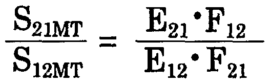
- the object in most devices such as a filter, a force balun, a balun, a capacitor, a resistor, and a coil, the object can be regarded as a kind of single chip because the object has no directionality. Therefore, by obtaining the ratio S 21M T / S 12MT transfer coefficient from the measurement result of the subject can determine the relationship of the error coefficients from Equation 5.
- the subject is not limited to two terminals, and can be applied to electronic components having three or more terminals if there is no direction between the ports.
- the transmission line of the present invention it is preferable to use a transmission line in which a signal conductor and a ground conductor are formed on the same plane.
- a coplanar waveguide / slot line can be used as a specific transmission line.
- the coplanar waveguide has a signal conductor and ground conductors on both sides of the signal conductor, and the signal conductor and the ground conductor are formed on the same plane. Specially suitable for raw measurement.
- a slot line in which a signal conductor and a ground conductor are provided on the same plane with an interval, is suitable for measuring high-frequency characteristics of 10 GHz or more.
- the desired distance between the multiple locations to which the short chip is connected is determined by the frequency to be measured, and should be less than or equal to lZl 6 to 3Z 16 and 5Zl 6 to 7/16 of the signal wavelength at the measurement frequency. desirable.
- the correction data be as far away from each other as possible.
- R RRR correction which obtains different correction data depending on the phase of the reflection of the short chip
- the data required for the correction are mutually different. ° Ideally, they are far apart.
- short-chip measurement should be performed at points separated by various distances, and these data should be selected and used as appropriate.
- phase difference of each data close to 120 ° .
- a short tip should be placed at a point 1/16 to 3/16 and 5/16 to 7/16 in electrical length from the subject measurement position. It is best to connect Brief Description of Drawings
- Figure 1a shows a measurement system using a conventional network analyzer and an error model for SOLT correction.
- Figure 1b shows a measurement system using a conventional network analyzer and an error model for TRL correction.
- FIG. 2 is a diagram illustrating the SOLT correction method.
- FIG. 3 is a diagram illustrating the TRL correction method. '
- FIG. 4 is a diagram in reflection measurement according to the present invention.
- FIG. 5 is a diagram in the through measurement according to the present invention.
- FIG. 6 is an error model diagram used in the correction method according to the present invention.
- FIG. 7 is a flowchart of an example of the correction method according to the present invention.
- FIG. 8 is a plan view at the time of correction of the high-frequency electrical characteristic measuring apparatus according to the present invention.
- FIG. 9 is a front view of the high-frequency electrical characteristic measuring apparatus shown in FIG. 8 at the time of correction.
- FIG. 10 is a front view of the high-frequency electrical characteristic measuring apparatus according to the present invention when measuring an object. ⁇
- FIG. 11 is a diagram showing the effect of stray capacitance generated between transmission paths.
- FIG. 12 is a high-frequency characteristic diagram of the chip resistance measured using the high-frequency electric characteristic measuring device according to the present invention. .
- FIG. 13 is a high-frequency characteristic diagram of the chip inductor measured using the high-frequency electrical characteristic measuring device according to the present invention.
- FIG. 14 is a diagram illustrating an example in which a series resonance occurs between the short chip and the transmission line.
- FIG. 15 is a plan view showing an example of a transmission line having three ports.
- FIG. 16 is a plan view of an example using a slot line as a transmission line.
- FIG. 17 is a plan view showing an example of a transmission line having one port.
- a measurement jig equipped with a transmission path of a length corresponding to the frequency bandwidth is required.
- a coplanar waveguide (hereinafter referred to as CPW) having a transmission line 12 on the front and a ground conductor 12d on the back is used as the measurement jig 11.
- the signal conductors 12a and 12b of the transmission line 12 were cut off at the center to support the series method.
- the short chip 10 In the RRRR correction, the short chip 10 must be measured at some positions on the transmission path 12 other than the measurement position of the subject. For this reason, as shown in FIG.
- the transmission line 12 has signal conductors 12 a and 12 b and ground conductors 12 c on both sides in the width direction. Both ends of the transmission line 12 are network analyzed via a coaxial cable 14.
- the 20 is connected to the measurement ports 21 to 24.
- the signal line 14a of the coaxial cable 14 is fixed to the signal conductors 12a and 12b by soldering, welding, or the like to eliminate connection variations.
- the measurement ports 21 and 24 are connected to the signal conductors 12a and 12b via the coaxial cable 14, and the measurement ports 22 and 23 are connected to the ground conductors 12c and 12d via the coaxial cable 14.
- RRR R correction is performed by measuring the short chip 10 at several points in the transmission path 12.
- the short chip 10 is shunt-connected between the signal conductor 12a of the transmission line 12 and the ground conductor 12c at the measurement position of the subject, and the electrical characteristics are measured.
- the same short chip 10 is measured at a position at a certain distance from this position. This time, measurements were made at a distance of 4 mm and 8 mm for the high-frequency region, but if measurement over a wide frequency range is required, it is desirable to increase the measurement positions as appropriate.
- the loss of the transmission line 12 is not large, the only difference between the two measurement results is the phase.
- the wavelength is 10 mm (wavelength of a 3 GHz electromagnetic wave in a vacuum)
- correction cannot be performed normally at a frequency of 1 Omm.
- the correction data be as far away from each other as possible.
- R RRR correction different correction data are obtained depending on the phase of the reflection of the short chip. Ideally, they should be 120 ° apart from each other.
- this condition is satisfied only at a specific frequency, when performing broadband measurement, short-chip measurement should be performed at points separated by various distances, and these data should be selected and used as appropriate.
- a short tip should be placed at a point about 1/16 to 3/16 and 5/16 to 7/16 in electrical length from the subject measurement position. It is best to connect When measuring a short chip, if an appropriate through chip is connected to the measurement position of the test object, if a contact failure occurs for any reason, the transfer coefficient between the ports will increase. Poor contact can be detected. As described above, since a measurement error can be detected during the correction procedure, it is possible to prevent waste such as being determined to have failed at the time when the subject is measured later. Soonore-measure-one
- the through chip 13 may be an element whose electrical characteristics are unknown, and it is only necessary that the transmission coefficient has no directionality. Measurement of one subject
- the subject 17 is connected to the transmission line, and its characteristics are measured.
- the test object 17 may be adsorbed by using a chip counter or the like, and the test object 17 may be brought into contact with the test object measurement position of the measurement jig 11 for measurement.
- a series connection can be made between the signal conductors 12a and 12b as shown in Fig. 10 (a). It may be connected between the signal conductors 12a, 12b and the ground conductor 12c as shown in FIG. Therefore, the measuring method according to the present invention can be applied to electronic components having three or more terminals, such as filters, in addition to electronic components having two terminals.
- the series method to which the RRRR method belongs should be able to support high impedance measurement if a high isolation measurement jig is used.However, a jig made of a material with a high dielectric constant such as glass epoxy material is used. If the thickness of the jig is as large as 1.6 mm, for example, the floating capacity between the ports will increase and the isolation will decrease. This problem will be reduced if a thin jig is made of a material having a low dielectric constant such as Teflon (registered trademark). Only However, if this is not enough, or if a jig with satisfactory characteristics cannot be used due to cost or other problems (Teflon substrates are generally expensive), this error can be corrected mathematically.
- Teflon substrates are generally expensive
- the floating admittance of the measurement result is obtained from the measurement result of the measuring jig alone (open state), and the influence of the floating admittance is mathematically removed from the measurement result of the test object.
- Z c be the impedance obtained by RRRR-correcting the measurement jig alone
- Z M be the impedance obtained by RRRR-correcting the test object measurement result.
- Impedance Z after the mathematical processing (open correction) L is obtained by the following equation. Too Z c is the dynamic range of the measurement system becomes narrow large, the measurement bar variability could cause problems such as increased, but should not use too isolators Deployment low jig, usually more Sufficient results can be obtained with the above processing.
- the impedance and the scattering coefficient are physical quantities that can be converted to each other, and indicate the characteristic impedance of the transmission line.
- the reflection coefficient of the scattering coefficient S 1: L, the transfer coefficient when the S 21, the scattering coefficient and impedance Z can be converted by the following equation. Although two equations are shown, both give the same result in principle.
- Figures 12 and 13 show the results of measurements of several impedance elements in the range of 1 GHz to 8 GHz using the above RRRR correction and open correction.
- the measured elements were an ImmX O. 5 mm chip resistor and several types of chip inductors (wound chip coils).
- Fig. 13 a general impedance characteristic curve of the inductor is obtained.
- the impedance increases in proportion to the frequency rise, and after the self-resonant frequency, the impedance decreases in inverse proportion to the frequency rise.
- Fig. 13 plots the theoretical calculated values of the impedance of the ideal inductor (series prefixed with SIM).
- RRRR correction is a method that has a characteristic in the method of calculating the error coefficient, and uses the same error model as TRL correction. For this reason, it has features similar to TRL correction. The following describes these features.
- transmission lines and connectors are required as standard equipment, and the electrical characteristics of the connection parts of these and the coaxial connector must all be equal.
- test object is inserted into the transmission line in series and measured.
- the length of the transmission path required for the measuring jig is determined by the lower limit of the frequency to be measured.
- a long transmission line is required to support low frequencies, and a short transmission line is sufficient to support high frequencies.
- the measurement for correction is performed by performing short-chip measurement at several places on the transmission line and through measurement using an appropriate device.
- the distance from the measurement position of the subject and how many short-chip measurements should be determined are determined by the measurement frequency bandwidth and the frequency upper limit. Also, the scattering coefficient is unknown if the through-chip does not have any directionality.
- R R R R correction can be performed on its own to correct errors in the entire measurement system. On the other hand, if RRR is corrected after correcting up to the coaxial connector that connects the jig board by a technique such as SOLT correction, the obtained error coefficient becomes the error coefficient of the jig board. In other words, the RRRR correction can be used as a method for identifying an error factor of the jig.
- Recent network analyzers have a function (de-embedding function) that automatically removes the influence of the applied error from the measurement results when an error coefficient such as a jig is given.
- an error coefficient such as a jig
- Unused function since there is no way to find the error of the jig, Unused function. This is a very useful function when combined with the RRRR correction method according to the present invention.
- Decoding is a technique for mathematically removing known error factors, and can be easily implemented using a transmission matrix.
- Scattering coefficient matrices of the error factor of the obtained jig is converted to a transmission matrix a material obtained by the inverse matrix, port 1 side, port 2 side their respective E one 1, and F- 1.
- the transmission matrix of the error factor of each port of the jig is EF.
- A be the transmission matrix of the device.
- the measurement result of measuring the device together with the jig using a network analyzer calibrated to the end of the coaxial cable is because the error of each port is superimposed on the device.
- each of the left and right E one 1, multiplying the F- 1 - and,
- the characteristics of the device can be obtained.
- the RRRR correction procedure that requires high-precision positioning of short chips is performed in a laboratory environment, and the error factors of each jig are determined with high accuracy, and the mass production process is performed. Can be mass-produced using jigs with known error factors. Of course, jig errors are eliminated by de-embedding the error factors found in the laboratory. .
- the measuring instrument is equipped with a calculator and a dedicated soft-tweeter.
- a calculator When the short-chip residual inductance and transmission path parameters (phase constant [rad / Hz] and transmission loss ⁇ [dB / Hz]) and the short-chip contact position are input,
- the standard device characteristics at the position are automatically calculated based on Equations 1 and 2, and this can be used for the correction calculations of Equations 3 to 6.
- the network analyzer can automatically predict the value of the standard device and make the RRRRR correction.
- the short chip 10 is floated from the transmission line 12 to obtain the capacitance C [F] generated between the transmission line and the short chip and the residual inductance of the short chip.
- the short chip 10 can be brought into contact with the transmission line 12 to resonate in series as shown in Fig. 14 (b). .
- a short-capacity capacitor may be used.
- the impedance of the short chip connection is 0 ⁇ , which is an ideal short-circuit state. In other words, the same effect as using a good short chip can be obtained at a high frequency where a good short chip cannot be obtained.
- Figure 15 shows an example of a measuring jig with three ports.
- 30 is a jig substrate
- 31 to 33 are three signal conductors formed on the upper surface of the jig substrate
- 34 is a signal conductor 31 to 3 on the upper surface of the jig substrate 30.
- 33 is a ground conductor formed so as to sandwich both sides
- 35 to 37 are connectors provided at the end of the jig board 30.
- One end of the signal conductors 3! To 3 3 is close to each other from three sides and faces each other, and the other end is connected to each of the connectors 35 to 37.
- Connect a short tip between each signal conductor 3 1 to 3 3 and the ground conductor 3 4 perform correction, and then between the signal conductors 3 1 to 3 3 or signal conductors 3 1 to 3 3 and ground.
- a subject 38 is connected between the conductor 32 and the electrical property is measured.
- the electrical characteristics of the subject 38 having three or more terminals can be measured.
- a slot line 40 as shown in FIG. 16 may be used.
- the signal conductors 41 and 42 and the ground conductor 43 are provided on the same plane with a gap.
- the subject 44 is connected between the signal conductors 41 and 42 or between the signal conductors 41 and 42 and the ground conductor 43 to measure the electrical characteristics.
- FIG. 17 shows an example of a jig used for the reflection method.
- 5.0 is a jig board
- 51 is one signal conductor
- 52 is a ground conductor provided on both sides of the signal conductor 51
- 53 is provided at one end of the jig board 50.
- the signal conductor 51 and the ground conductor 52 are formed on the same plane on the jig substrate 50.
- One end of the signal conductor 51 is an open end, and the other end is connected to the connector 53.
- the reflection method is a method of observing how much of the electromagnetic wave incident on the subject 54 from one port (connector 53) is reflected, and obtaining the impedance or the like from this, and is one port. error factor from even ⁇ ⁇ , ( ⁇ 21 ⁇ ⁇ 12), ⁇ 22 tooth force stomach. By the way, it is not necessary to obtain ⁇ 21 and ⁇ ⁇ ⁇ 12 separately.
- the reflection coefficient St1 ⁇ of the subject can be obtained by the following equation.
- S 11M is a measured reflection coefficient. In this case, no through measurement is required.
- the series resonance of the short chip shown in FIG. 14 may be used.
- the method for measuring high-frequency electrical characteristics according to the present invention is not limited to the above embodiment.
- the measuring device in the present invention is not limited to a network analyzer, and any device that can measure high-frequency electrical characteristics can be used.
- the transmission path is not limited to a plane transmission path, but can be a shunt connection of a short chip, a series connection of a through chip, and can connect a subject between signal conductors or between multiple signal conductors and a ground conductor. If so, any structure can be used.
- the method for measuring high-frequency electrical characteristics according to the present invention has the following effects. '
- the test object can be measured not only with two terminals but also with electronic parts with three or more terminals. Therefore, the present invention is very useful for accurately measuring the scattering coefficient and impedance value of electronic components such as filters, force brass and baluns, or impedance elements such as chip inductors and chip capacitors using a high-frequency electrical characteristic measuring device. This is an effective method.
Landscapes
- Physics & Mathematics (AREA)
- General Physics & Mathematics (AREA)
- Measurement Of Resistance Or Impedance (AREA)
Abstract
Description




Claims


Priority Applications (9)
| Application Number | Priority Date | Filing Date | Title |
|---|---|---|---|
| PCT/JP2004/004882 WO2005101037A1 (ja) | 2004-04-02 | 2004-04-02 | 電子部品の高周波電気特性測定方法および装置 |
| DE112004002808.6T DE112004002808B4 (de) | 2004-04-02 | 2004-12-21 | Verfahren und Gerät zum Messen von elektrischen Hochfrequenzcharakteristika einer elektronischen Vorrichtung und Verfahren zum Kalibrieren von Geräten zum Messen von elektrischen Hochfrequenzcharakteristika |
| DE112004002805.1T DE112004002805B4 (de) | 2004-04-02 | 2004-12-21 | Verfahren und Vorrichtung zum Messen von elektrischen Hochfrequenzcharakteristika einer elektronischen Vorrichtung und Verfahren zum Kalibrieren von Vorrichtungen zum Messen von elektrischen Hochfrequenzcharakteristika |
| JP2006512253A JP3912428B2 (ja) | 2004-04-02 | 2004-12-21 | 電子部品の高周波電気特性測定方法および装置、高周波電気特性測定装置の校正方法 |
| PCT/JP2004/019086 WO2005101034A1 (ja) | 2004-04-02 | 2004-12-21 | 電子部品の高周波電気特性測定方法および装置、高周波電気特性測定装置の校正方法 |
| JP2006512254A JP3912429B2 (ja) | 2004-04-02 | 2004-12-21 | 電子部品の高周波電気特性測定方法および装置、高周波電気特性測定装置の校正方法 |
| PCT/JP2004/019087 WO2005101035A1 (ja) | 2004-04-02 | 2004-12-21 | 電子部品の高周波電気特性測定方法および装置、高周波電気特性測定装置の校正方法 |
| US11/537,111 US7439748B2 (en) | 2004-04-02 | 2006-09-29 | Method and apparatus for measuring high-frequency electrical characteristics of electronic device, and method for calibrating apparatus for measuring high-frequency electrical characteristics |
| US11/536,915 US7375534B2 (en) | 2004-04-02 | 2006-09-29 | Method and apparatus for measuring high-frequency electrical characteristics of electronic device, and method for calibrating apparatus for measuring high-frequency electrical characteristics |
Applications Claiming Priority (1)
| Application Number | Priority Date | Filing Date | Title |
|---|---|---|---|
| PCT/JP2004/004882 WO2005101037A1 (ja) | 2004-04-02 | 2004-04-02 | 電子部品の高周波電気特性測定方法および装置 |
Related Parent Applications (1)
| Application Number | Title | Priority Date | Filing Date |
|---|---|---|---|
| PCT/JP2004/019087 Continuation WO2005101035A1 (ja) | 2004-04-02 | 2004-12-21 | 電子部品の高周波電気特性測定方法および装置、高周波電気特性測定装置の校正方法 |
Related Child Applications (3)
| Application Number | Title | Priority Date | Filing Date |
|---|---|---|---|
| PCT/JP2004/019086 Continuation WO2005101034A1 (ja) | 2004-04-02 | 2004-12-21 | 電子部品の高周波電気特性測定方法および装置、高周波電気特性測定装置の校正方法 |
| US11/536,915 Continuation US7375534B2 (en) | 2004-04-02 | 2006-09-29 | Method and apparatus for measuring high-frequency electrical characteristics of electronic device, and method for calibrating apparatus for measuring high-frequency electrical characteristics |
| US11/537,111 Continuation US7439748B2 (en) | 2004-04-02 | 2006-09-29 | Method and apparatus for measuring high-frequency electrical characteristics of electronic device, and method for calibrating apparatus for measuring high-frequency electrical characteristics |
Publications (1)
| Publication Number | Publication Date |
|---|---|
| WO2005101037A1 true WO2005101037A1 (ja) | 2005-10-27 |
Family
ID=35150130
Family Applications (3)
| Application Number | Title | Priority Date | Filing Date |
|---|---|---|---|
| PCT/JP2004/004882 Ceased WO2005101037A1 (ja) | 2004-04-02 | 2004-04-02 | 電子部品の高周波電気特性測定方法および装置 |
| PCT/JP2004/019086 Ceased WO2005101034A1 (ja) | 2004-04-02 | 2004-12-21 | 電子部品の高周波電気特性測定方法および装置、高周波電気特性測定装置の校正方法 |
| PCT/JP2004/019087 Ceased WO2005101035A1 (ja) | 2004-04-02 | 2004-12-21 | 電子部品の高周波電気特性測定方法および装置、高周波電気特性測定装置の校正方法 |
Family Applications After (2)
| Application Number | Title | Priority Date | Filing Date |
|---|---|---|---|
| PCT/JP2004/019086 Ceased WO2005101034A1 (ja) | 2004-04-02 | 2004-12-21 | 電子部品の高周波電気特性測定方法および装置、高周波電気特性測定装置の校正方法 |
| PCT/JP2004/019087 Ceased WO2005101035A1 (ja) | 2004-04-02 | 2004-12-21 | 電子部品の高周波電気特性測定方法および装置、高周波電気特性測定装置の校正方法 |
Country Status (3)
| Country | Link |
|---|---|
| JP (2) | JP3912428B2 (ja) |
| DE (2) | DE112004002808B4 (ja) |
| WO (3) | WO2005101037A1 (ja) |
Families Citing this family (4)
| Publication number | Priority date | Publication date | Assignee | Title |
|---|---|---|---|---|
| WO2006090550A1 (ja) * | 2005-02-22 | 2006-08-31 | Murata Manufacturing Co., Ltd. | 伝送路材料の誘電率測定方法およびこの誘電率測定方法を用いた電子部品の電気特性測定方法 |
| WO2008065791A1 (en) | 2006-11-30 | 2008-06-05 | Murata Manufacturing Co., Ltd. | High frequency characteristics error correction method of electronic component |
| JP2012198182A (ja) * | 2011-03-23 | 2012-10-18 | Fujitsu Ltd | 校正基板および回路パラメータの測定方法 |
| JP7153309B2 (ja) * | 2018-06-04 | 2022-10-14 | 国立研究開発法人産業技術総合研究所 | ベクトルネットワークアナライザを用いた反射係数の測定方法 |
Citations (2)
| Publication number | Priority date | Publication date | Assignee | Title |
|---|---|---|---|---|
| DE4313705A1 (de) * | 1992-05-02 | 1993-11-04 | Rohde & Schwarz | Verfahren zum kalibrieren eines netzwerkanalysators |
| JPH11211766A (ja) * | 1998-01-26 | 1999-08-06 | Advantest Corp | 自動キャリブレーション装置 |
Family Cites Families (7)
| Publication number | Priority date | Publication date | Assignee | Title |
|---|---|---|---|---|
| JPH0354649A (ja) * | 1989-07-24 | 1991-03-08 | Oki Electric Ind Co Ltd | バッファ記憶制御方式 |
| JPH0784879A (ja) * | 1993-09-09 | 1995-03-31 | Toshiba Corp | キャッシュメモリ装置 |
| DE4433375C2 (de) * | 1993-10-26 | 1998-07-02 | Rohde & Schwarz | Verfahren zum Kalibrieren eines Netzwerkanalysators |
| JP3404238B2 (ja) * | 1997-01-10 | 2003-05-06 | 京セラ株式会社 | 高周波測定の校正標準器および校正法ならびに高周波用伝送線路の伝送損失の測定方法 |
| JP2000029788A (ja) * | 1998-07-15 | 2000-01-28 | Nec Corp | キャッシュメモリシステム及びそれに用いるキャッシュ制御方法並びにその制御プログラムを記録した記録媒体 |
| JP2001222467A (ja) * | 2000-02-07 | 2001-08-17 | Matsushita Electric Ind Co Ltd | キャッシュ装置 |
| DE10242932B4 (de) * | 2002-09-16 | 2009-02-05 | Rohde & Schwarz Gmbh & Co. Kg | Das LRR-Verfahren zur Kalibrierung von vektoriellen 4-Messstellen-Netzwerkanalysatoren |
-
2004
- 2004-04-02 WO PCT/JP2004/004882 patent/WO2005101037A1/ja not_active Ceased
- 2004-12-21 DE DE112004002808.6T patent/DE112004002808B4/de not_active Expired - Fee Related
- 2004-12-21 WO PCT/JP2004/019086 patent/WO2005101034A1/ja not_active Ceased
- 2004-12-21 DE DE112004002805.1T patent/DE112004002805B4/de not_active Expired - Fee Related
- 2004-12-21 JP JP2006512253A patent/JP3912428B2/ja not_active Expired - Lifetime
- 2004-12-21 JP JP2006512254A patent/JP3912429B2/ja not_active Expired - Lifetime
- 2004-12-21 WO PCT/JP2004/019087 patent/WO2005101035A1/ja not_active Ceased
Patent Citations (2)
| Publication number | Priority date | Publication date | Assignee | Title |
|---|---|---|---|---|
| DE4313705A1 (de) * | 1992-05-02 | 1993-11-04 | Rohde & Schwarz | Verfahren zum kalibrieren eines netzwerkanalysators |
| JPH11211766A (ja) * | 1998-01-26 | 1999-08-06 | Advantest Corp | 自動キャリブレーション装置 |
Also Published As
| Publication number | Publication date |
|---|---|
| JP3912429B2 (ja) | 2007-05-09 |
| JP3912428B2 (ja) | 2007-05-09 |
| JPWO2005101035A1 (ja) | 2008-03-06 |
| DE112004002805B4 (de) | 2017-09-21 |
| WO2005101035A1 (ja) | 2005-10-27 |
| JPWO2005101034A1 (ja) | 2008-03-06 |
| DE112004002808B4 (de) | 2017-09-21 |
| WO2005101034A1 (ja) | 2005-10-27 |
| DE112004002805T5 (de) | 2007-02-01 |
| DE112004002808T5 (de) | 2007-02-15 |
Similar Documents
| Publication | Publication Date | Title |
|---|---|---|
| WO2008029522A1 (en) | Passive intermodulation distortion measuring method and system | |
| US20100001742A1 (en) | Calibration technique | |
| CN109239480B (zh) | 一种传输线、散射参数测试系统及方法 | |
| US10001521B1 (en) | Transistor test fixture with integrated couplers and method | |
| CN104297567B (zh) | 用于测量超高频射频识别电子标签上天线阻抗的夹具 | |
| US7173433B2 (en) | Circuit property measurement method | |
| US20030115008A1 (en) | Test fixture with adjustable pitch for network measurement | |
| TWI237120B (en) | Impedance standard substrate and method for calibrating vector network analyzer | |
| US7439748B2 (en) | Method and apparatus for measuring high-frequency electrical characteristics of electronic device, and method for calibrating apparatus for measuring high-frequency electrical characteristics | |
| US7405576B2 (en) | Method and apparatus for measuring high-frequency electrical characteristics of electronic device, and method for calibrating apparatus for measuring high-frequency electrical characteristics | |
| JP4650487B2 (ja) | 伝送路材料の誘電率測定方法およびこの誘電率測定方法を用いた電子部品の電気特性測定方法 | |
| US9568568B2 (en) | Apparatus and method of measuring permeability of a sample across which a DC voltage is being applied | |
| US7095294B2 (en) | Directional bridge coupler | |
| US7375534B2 (en) | Method and apparatus for measuring high-frequency electrical characteristics of electronic device, and method for calibrating apparatus for measuring high-frequency electrical characteristics | |
| CN115372665A (zh) | 射频器件测试装置和测试系统 | |
| WO2005101037A1 (ja) | 電子部品の高周波電気特性測定方法および装置 | |
| US8502619B2 (en) | Circuit module and measurement method | |
| CN117368820B (zh) | 一种校准装置、差分夹具以及相关装置和系统 | |
| JP3912427B2 (ja) | 電子部品の高周波電気特性測定方法および装置、高周波電気特性測定装置の校正方法 | |
| JP2003232834A (ja) | 高周波・高速用デバイスの検査方法および検査治具 | |
| JP5675461B2 (ja) | プローブ、測定装置、および、回路基板 | |
| CN118937786A (zh) | 一种毫米波频段耦合功率探头和功率探测方法 | |
| JP2025022752A (ja) | 透磁率測定治具および透磁率測定方法 | |
| CN104081212B (zh) | 射频连接器、射频单板及校准器件 | |
| CN120254546A (zh) | 一种基于PoP封装结构的传输线去嵌方法和系统 |
Legal Events
| Date | Code | Title | Description |
|---|---|---|---|
| AK | Designated states |
Kind code of ref document: A1 Designated state(s): AE AG AL AM AT AU AZ BA BB BG BR BW BY BZ CA CH CN CO CR CU CZ DE DK DM DZ EC EE EG ES FI GB GD GE GH GM HR HU ID IL IN IS JP KE KG KP KR KZ LC LK LR LS LT LU LV MA MD MG MK MN MW MX MZ NA NI NO NZ OM PG PH PL PT RO RU SC SD SE SG SK SL SY TJ TM TN TR TT TZ UA UG US UZ VC VN YU ZA ZM ZW |
|
| AL | Designated countries for regional patents |
Kind code of ref document: A1 Designated state(s): BW GH GM KE LS MW MZ SD SL SZ TZ UG ZM ZW AM AZ BY KG KZ MD RU TJ TM AT BE BG CH CY CZ DE DK EE ES FI FR GB GR HU IE IT LU MC NL PL PT RO SE SI SK TR BF BJ CF CG CI CM GA GN GQ GW ML MR NE SN TD TG |
|
| 121 | Ep: the epo has been informed by wipo that ep was designated in this application | ||
| WWE | Wipo information: entry into national phase |
Ref document number: 11537111 Country of ref document: US Ref document number: 11536915 Country of ref document: US |
|
| NENP | Non-entry into the national phase |
Ref country code: DE |
|
| WWW | Wipo information: withdrawn in national office |
Country of ref document: DE |
|
| WWP | Wipo information: published in national office |
Ref document number: 11536915 Country of ref document: US Ref document number: 11537111 Country of ref document: US |
|
| 122 | Ep: pct application non-entry in european phase |