US9899000B2 - Display, display control method, display control device, and electronic apparatus - Google Patents
Display, display control method, display control device, and electronic apparatus Download PDFInfo
- Publication number
- US9899000B2 US9899000B2 US14/422,103 US201414422103A US9899000B2 US 9899000 B2 US9899000 B2 US 9899000B2 US 201414422103 A US201414422103 A US 201414422103A US 9899000 B2 US9899000 B2 US 9899000B2
- Authority
- US
- United States
- Prior art keywords
- image
- display
- light
- light emission
- section
- Prior art date
- Legal status (The legal status is an assumption and is not a legal conclusion. Google has not performed a legal analysis and makes no representation as to the accuracy of the status listed.)
- Expired - Fee Related
Links
Images


Classifications
-
- G—PHYSICS
- G09—EDUCATION; CRYPTOGRAPHY; DISPLAY; ADVERTISING; SEALS
- G09G—ARRANGEMENTS OR CIRCUITS FOR CONTROL OF INDICATING DEVICES USING STATIC MEANS TO PRESENT VARIABLE INFORMATION
- G09G5/00—Control arrangements or circuits for visual indicators common to cathode-ray tube indicators and other visual indicators
- G09G5/10—Intensity circuits
-
- G—PHYSICS
- G09—EDUCATION; CRYPTOGRAPHY; DISPLAY; ADVERTISING; SEALS
- G09G—ARRANGEMENTS OR CIRCUITS FOR CONTROL OF INDICATING DEVICES USING STATIC MEANS TO PRESENT VARIABLE INFORMATION
- G09G3/00—Control arrangements or circuits, of interest only in connection with visual indicators other than cathode-ray tubes
- G09G3/20—Control arrangements or circuits, of interest only in connection with visual indicators other than cathode-ray tubes for presentation of an assembly of a number of characters, e.g. a page, by composing the assembly by combination of individual elements arranged in a matrix no fixed position being assigned to or needed to be assigned to the individual characters or partial characters
- G09G3/34—Control arrangements or circuits, of interest only in connection with visual indicators other than cathode-ray tubes for presentation of an assembly of a number of characters, e.g. a page, by composing the assembly by combination of individual elements arranged in a matrix no fixed position being assigned to or needed to be assigned to the individual characters or partial characters by control of light from an independent source
- G09G3/3406—Control of illumination source
- G09G3/3413—Details of control of colour illumination sources
-
- G—PHYSICS
- G09—EDUCATION; CRYPTOGRAPHY; DISPLAY; ADVERTISING; SEALS
- G09G—ARRANGEMENTS OR CIRCUITS FOR CONTROL OF INDICATING DEVICES USING STATIC MEANS TO PRESENT VARIABLE INFORMATION
- G09G3/00—Control arrangements or circuits, of interest only in connection with visual indicators other than cathode-ray tubes
- G09G3/20—Control arrangements or circuits, of interest only in connection with visual indicators other than cathode-ray tubes for presentation of an assembly of a number of characters, e.g. a page, by composing the assembly by combination of individual elements arranged in a matrix no fixed position being assigned to or needed to be assigned to the individual characters or partial characters
- G09G3/34—Control arrangements or circuits, of interest only in connection with visual indicators other than cathode-ray tubes for presentation of an assembly of a number of characters, e.g. a page, by composing the assembly by combination of individual elements arranged in a matrix no fixed position being assigned to or needed to be assigned to the individual characters or partial characters by control of light from an independent source
- G09G3/36—Control arrangements or circuits, of interest only in connection with visual indicators other than cathode-ray tubes for presentation of an assembly of a number of characters, e.g. a page, by composing the assembly by combination of individual elements arranged in a matrix no fixed position being assigned to or needed to be assigned to the individual characters or partial characters by control of light from an independent source using liquid crystals
- G09G3/3611—Control of matrices with row and column drivers
- G09G3/3696—Generation of voltages supplied to electrode drivers
-
- G—PHYSICS
- G09—EDUCATION; CRYPTOGRAPHY; DISPLAY; ADVERTISING; SEALS
- G09G—ARRANGEMENTS OR CIRCUITS FOR CONTROL OF INDICATING DEVICES USING STATIC MEANS TO PRESENT VARIABLE INFORMATION
- G09G5/00—Control arrangements or circuits for visual indicators common to cathode-ray tube indicators and other visual indicators
- G09G5/18—Timing circuits for raster scan displays
-
- G—PHYSICS
- G09—EDUCATION; CRYPTOGRAPHY; DISPLAY; ADVERTISING; SEALS
- G09G—ARRANGEMENTS OR CIRCUITS FOR CONTROL OF INDICATING DEVICES USING STATIC MEANS TO PRESENT VARIABLE INFORMATION
- G09G2310/00—Command of the display device
- G09G2310/02—Addressing, scanning or driving the display screen or processing steps related thereto
- G09G2310/0235—Field-sequential colour display
-
- G—PHYSICS
- G09—EDUCATION; CRYPTOGRAPHY; DISPLAY; ADVERTISING; SEALS
- G09G—ARRANGEMENTS OR CIRCUITS FOR CONTROL OF INDICATING DEVICES USING STATIC MEANS TO PRESENT VARIABLE INFORMATION
- G09G2320/00—Control of display operating conditions
- G09G2320/02—Improving the quality of display appearance
- G09G2320/0242—Compensation of deficiencies in the appearance of colours
-
- G—PHYSICS
- G09—EDUCATION; CRYPTOGRAPHY; DISPLAY; ADVERTISING; SEALS
- G09G—ARRANGEMENTS OR CIRCUITS FOR CONTROL OF INDICATING DEVICES USING STATIC MEANS TO PRESENT VARIABLE INFORMATION
- G09G2320/00—Control of display operating conditions
- G09G2320/06—Adjustment of display parameters
- G09G2320/0613—The adjustment depending on the type of the information to be displayed
- G09G2320/062—Adjustment of illumination source parameters
-
- G—PHYSICS
- G09—EDUCATION; CRYPTOGRAPHY; DISPLAY; ADVERTISING; SEALS
- G09G—ARRANGEMENTS OR CIRCUITS FOR CONTROL OF INDICATING DEVICES USING STATIC MEANS TO PRESENT VARIABLE INFORMATION
- G09G2320/00—Control of display operating conditions
- G09G2320/06—Adjustment of display parameters
- G09G2320/0626—Adjustment of display parameters for control of overall brightness
- G09G2320/064—Adjustment of display parameters for control of overall brightness by time modulation of the brightness of the illumination source
-
- G—PHYSICS
- G09—EDUCATION; CRYPTOGRAPHY; DISPLAY; ADVERTISING; SEALS
- G09G—ARRANGEMENTS OR CIRCUITS FOR CONTROL OF INDICATING DEVICES USING STATIC MEANS TO PRESENT VARIABLE INFORMATION
- G09G2320/00—Control of display operating conditions
- G09G2320/06—Adjustment of display parameters
- G09G2320/0626—Adjustment of display parameters for control of overall brightness
- G09G2320/0646—Modulation of illumination source brightness and image signal correlated to each other
-
- G—PHYSICS
- G09—EDUCATION; CRYPTOGRAPHY; DISPLAY; ADVERTISING; SEALS
- G09G—ARRANGEMENTS OR CIRCUITS FOR CONTROL OF INDICATING DEVICES USING STATIC MEANS TO PRESENT VARIABLE INFORMATION
- G09G3/00—Control arrangements or circuits, of interest only in connection with visual indicators other than cathode-ray tubes
- G09G3/20—Control arrangements or circuits, of interest only in connection with visual indicators other than cathode-ray tubes for presentation of an assembly of a number of characters, e.g. a page, by composing the assembly by combination of individual elements arranged in a matrix no fixed position being assigned to or needed to be assigned to the individual characters or partial characters
- G09G3/34—Control arrangements or circuits, of interest only in connection with visual indicators other than cathode-ray tubes for presentation of an assembly of a number of characters, e.g. a page, by composing the assembly by combination of individual elements arranged in a matrix no fixed position being assigned to or needed to be assigned to the individual characters or partial characters by control of light from an independent source
- G09G3/36—Control arrangements or circuits, of interest only in connection with visual indicators other than cathode-ray tubes for presentation of an assembly of a number of characters, e.g. a page, by composing the assembly by combination of individual elements arranged in a matrix no fixed position being assigned to or needed to be assigned to the individual characters or partial characters by control of light from an independent source using liquid crystals
Definitions
- the present disclosure relates to a display that includes a backlight, a display control method and a display control device used in such a display, and an electronic apparatus including such a display.
- a display is applied to various types of electronic apparatus with diversification and multi-functionalization of the electronic apparatus.
- the display is applied to a stationary display such as a television receiver (a television apparatus), a display of portable electronic apparatus (a portable terminal) such as a mobile phone, a projection type display such as a projector, and a wearable display such as a head mounted display.
- the display may generate light of any color by combining together light beams of, for example, red (R), green (G), and blue (B) (primary colors) so as to perform display with the light of any color.
- a display such as, for example, a liquid crystal display that may include a plurality of pixels each including red, green, and blue sub-pixels so as to perform display using the plurality of pixels.
- another display such as, for example, a projector that may include red, green, and blue display devices and an optical component such as a prism or the like so as to perform display by overlapping, by the optical component, images that the above-mentioned display devices have generated.
- a so-called field sequential driving type display that may perform display of red, green, and blue in time division (for example, Patent Literatures 1 and 2).
- a display be high in image quality and further improvement in image quality of the display is expected.
- a display includes: a predetermined number of light emitting sections configured to emit respective color light beams having respective colors that are different from one another; a light emission control section configured to determine, out of the predetermined number of light emitting sections, one or a plurality of light emitting sections caused to perform light emission in each frame period, and control the light emission of the determined one or the plurality of light emitting sections; and a display section configured to perform display by allowing the color light beams to transmit therethrough or by reflecting the color light beams.
- a display device configured to display at least one image, and includes: at least one light emitter configured to emit a plurality of colored light beams, each of the plurality of colored light beams being a respective color different than the others; and a light emission controller configured to determine, based on at least one characteristic of the at least one image, one or more light beams of the plurality of colored light beams to emit in a frame period corresponding to the at least one image.
- a display control device is configured, for a display section configured to perform display by allowing color light beams to transmit therethrough or by reflecting the color light beams, to determine, out of a predetermined number of light emitting sections configured to emit the respective color light beams having respective colors that are different from one another, one or a plurality of light emitting sections caused to perform light emission in each frame period, and control the light emission of the determined one or the plurality of light emitting sections.
- a light emission controller is configured to control at least one light emitter, and includes: an analyzer configured to: receive a plurality of image signals, each of the plurality of image signals corresponding to a respective color; create a plurality of comparison results by comparing a plurality of luminance values, based on a respective one of the plurality of image signals, to at least one threshold value; and determine which of the plurality of image signals to display based on the plurality of comparison results; and a controller configured to control the at least one light emitter based on the determination of the analyzer.
- a light emitting device includes: a plurality of light emitters, each of the plurality of light emitters configured to emit light of a different color; a light emission controller configured to: receive a plurality of image signals, each of the image signals corresponding to a respective one of the plurality of colors; determine at least one of the plurality of light emitters to emit light based on the plurality of image signals; and output a control signal to each of the plurality of light emitters based on the determination of the light emission controller.
- the display control method, the display control device, and the electronic apparatus in the above-described embodiments of the present disclosure out of the predetermined number of light emitting sections, the one or the plurality of light emitting sections that is/are made to emit light in each of the frame periods is/are determined. Therefore, it is possible to improve the image quality.
- FIG. 1 is a block diagram illustrating one configuration example of a display according to an embodiment of the present disclosure.
- FIG. 2 is a block diagram illustrating one configuration example of a liquid crystal display section illustrated in FIG. 1 .
- FIG. 3 is an explanatory diagram illustrating one configuration example of a backlight illustrated in FIG. 1 .
- FIG. 4 is a timing chart illustrating one operation example of the display illustrated in FIG. 1 .
- FIG. 5 is a timing chart illustrating another operational example of the display illustrated in FIG. 1 .
- FIG. 6 is a timing chart illustrating still another operational example of the display illustrated in FIG. 1 .
- FIG. 7 is a block diagram illustrating one configuration example of a display according to a comparative example.
- FIG. 8 is a timing chart illustrating one operational example of the display illustrated in FIG. 7 .
- FIG. 9 is a timing chart illustrating another operational example of the display illustrated in FIG. 7 .
- FIG. 10 is a timing chart illustrating one operational example of a display according to one modification example.
- FIG. 11 a timing chart illustrating one operational example of a display according to another modification example.
- FIG. 12 a timing chart illustrating one operational example of a display according to still another modification example.
- FIG. 13 a timing chart illustrating one operational example of a display according to still another modification example.
- FIG. 14 is another timing chart illustrating one operational example of the display illustrated in FIG. 7 .
- FIG. 15 is a timing chart illustrating one operational example of a display according to still another modification example.
- FIG. 16 is a block diagram illustrating one configuration example of a display according to still another modification example.
- FIG. 17 is a timing chart illustrating one operational example of the display illustrated in FIG. 16 .
- FIG. 18 is a timing chart illustrating one operational example of a display according to still another modification example.
- FIG. 19 is a timing chart illustrating one operational example of a display according to still another modification example.
- FIG. 20 is a timing chart illustrating one operational example of a display according to still another modification example.
- FIG. 21 is a block diagram illustrating one configuration example of a display according to still another modification example.
- FIG. 22 is a block diagram illustrating one configuration example of a display according to still another modification example.
- FIG. 23 is a block diagram illustrating one configuration example of a display according to still another modification example.
- FIG. 24 is a block diagram illustrating one configuration example of a display according to still another modification example.
- FIG. 25 is a block diagram illustrating one configuration example of a display according to still another modification example.
- FIG. 26 is a block diagram illustrating one configuration example of a display according to still another modification example.
- FIG. 27 is a perspective view illustrating one external configuration example of a television apparatus to which the display according to one embodiment of the present disclosure has been applied.
- FIG. 28 is an explanatory diagram illustrating one configuration example of a backlight according to another modification example.
- FIG. 29 is a schematic diagram illustrating one configuration example of a projector to which the display according to one embodiment of the present disclosure has been applied.
- FIG. 1 illustrates one configuration example of a display according to an embodiment of the present disclosure.
- a display 1 is a display that operates by a so-called field sequential driving scheme. It is to be noted that since a display control method and a display control device according to embodiments of the present disclosure are embodied by the present embodiment, description thereof will be made together with description of the display 1 .
- the display 1 includes an image input section 11 , a color correction section 12 , a memory 9 , a memory control section 13 , a signal correction section 14 , a liquid crystal display section 20 , an analysis section 15 , a threshold value setting section 16 , a control section 17 , a backlight control section 18 , and a backlight 30 .
- the image input section 11 is an interface used to input an image signal which may be an RGB signal from external equipment such as a PC (Personal Computer) and so forth.
- the image input section 11 is adapted to output the image signal so input as image signals SR 1 , SG 1 , and SB 1 , and a synchronous signal Sync 1 that synchronizes with the image signals SR 1 , SG 1 , and SB 1 .
- the image signal SR 1 is a signal that includes luminance information IR of red (R)
- the image signal SG 1 is a signal that includes luminance information IG of green (G)
- the image signal SB 1 is a signal that includes luminance information IB of blue (B).
- the color correction section 12 is adapted to perform color-related correction such as gamma correction, color irregularity correction and so forth on the basis of the image signals SR 1 , SG 1 , and SB 1 , and the synchronous signal Sync 1 .
- the color correction section 12 is configured to generate image signals SR 2 , SG 2 , and SB 2 by performing such correction as mentioned above, and to generate a synchronous signal Sync 2 that synchronizes with the image signals SR 2 , SG 2 , and SB 2 . It is to be noted that although in this example, the color correction section 12 is configured to perform the color-related correction, the color correction section 12 may be configured to perform signal processing other than the color-related correction.
- the memory 9 is a so-called frame memory that stores the luminance information IR included in the image signal SR 2 , the luminance information IG included in the image signal SG 2 , and the luminance information IB included in the image signal SB 2 each by the amount of one frame.
- the memory 9 is configured such that operations of writing and reading-out the pieces of luminance information IR, IG, and IB into and from the memory 9 are controlled by the memory control section 13 .
- the memory control section 13 is adapted to control the operations of writing and reading-out the pieces of luminance information IR, IG, and IB into and from the memory 9 . Specifically, in the writing operation, the memory control section 13 makes the memory 9 store the pieces of luminance information IR, IG, and IB included in the image signals SR 2 , SG 2 , and SB 2 on the basis of the image signals SR 2 , SG 2 , and SB 2 , and the synchronous signal Sync 2 . Thus, for example, the pieces of luminance information IR, IG, and IB corresponding to one frame may be stored into the memory 9 .
- the memory control section 13 reads out only the luminance information to be displayed out of the pieces of one-frame luminance information IR, IG, and IB from the memory 9 in instructed order on the basis of a memory control signal SMEM as described later. Specifically, the memory control section 13 sequentially reads out any of the one-frame luminance information IR (a red image PR), the one-frame luminance information IG (a green image PG), and the one-frame luminance information IB (a blue image PB) in each subfield SF (described later) on the basis of the memory control signal SMEM.
- the one-frame luminance information IR a red image PR
- the one-frame luminance information IG a green image PG
- IB a blue image PB
- the memory control section 13 reads out only an image to be displayed out of the red image PR, the green image PG, and the blue image PB.
- the memory control section 13 is configured to then output one or more of the pieces of luminance information IR, IG, and IB read out from the memory 9 as an image signal SIG 3 (a field sequential signal), and to generate and output a synchronous signal Sync 3 that synchronizes with the image signal SIG 3 .
- the signal correction section 14 is adapted to perform signal correction on the basis of the image signal SIG 3 and the synchronous signal Sync 3 .
- the signal correction section 14 may be adapted to correct the one or more pieces of luminance information IR, IG, and IB on the basis of, for example, the one or more pieces of luminance information IR, IG, and IB in the plurality of adjacent subfields SF (described later).
- One example of such correction may include overdrive correction.
- the signal correction section 14 is configured to generate an image signal SIG 4 by performing the above-mentioned correction, and to generate a synchronous signal Sync 4 that synchronizes with the image signal SIG 4 .
- the liquid crystal display section 20 is adapted to perform display by driving liquid crystal display elements and modulating light emitted from the backlight 30 .
- FIG. 2 illustrates one example of a block diagram of the liquid crystal display section 20 .
- the liquid crystal display section 20 includes a timing control section 21 , a gate driver 22 , a data driver 23 , and a pixel array section 24 .
- the timing control section 21 is adapted to control drive timings of the gate driver 22 and the data driver 23 on the basis of the image signal SIG 4 and the synchronous signal Sync 4 , to generate an image signal Sdisp on the basis of the image signal SIG 4 , and to supply the image signal Sdisp to the data driver 23 .
- the gate driver 22 is adapted to sequentially select and sequentially scan pixels Pix in the pixel array section 24 row by row in accordance with timing control by the timing control section 21 .
- the data driver 23 is adapted to generate a pixel voltage Vpix which is an analog signal by performing D/A (digital/analog) conversion on the basis of the image signal Sdisp and to supply the pixel voltage Vpix to each pixel Pix in the pixel array section 24 .
- the pixel array section 24 is a section in which the pixels Pix are arranged in a matrix.
- Each pixel Pix is adapted to perform display in time division on the basis of the pixel voltage Vpix corresponding to the luminance information IR, the pixel voltage Vpix corresponding to the luminance information IG, and the pixel voltage Vpix corresponding to the luminance information IB. That is, each pixel Pix does not include so-called sub-pixels and is configured to perform display of red, green, and blue in time division.
- the backlight 30 emits red light, green light, and blue light in time division in synchronization with a displaying operation on the pixel array section 24 as described later.
- the display 1 displays the red image PR, the green image PG, and the blue image PB in time division.
- the analysis section 15 is adapted to determine the image to be displayed out of the red image PR, the green image PG, and the blue image PB on the basis of the image signals SR 2 , SG 2 , and SB 2 and the synchronous signal Sync 1 and to output a result of determination as color information CI.
- the analysis section 15 may obtain a histogram concerning to luminance levels of, for example, the image signal SR 2 on the basis of the one-frame luminance information IR included in the image signal SR 2 , and may determine that the red image PR is to be displayed when the luminance levels are equal to or are distributed above a predetermined luminance level (a threshold value Lth).
- the analysis section 15 determines that the red image is not to be displayed when all of the luminance levels of the one-frame luminance information IR are less than the threshold value Lth.
- the analysis section 15 determines whether the green image PG is to be displayed on the basis of the one-frame luminance information IG included in the image signal SG 2 and determines whether the blue image PB is to be displayed on the basis of the one-frame luminance information IB included in the image signal SB 2 in the same way. Then, the analysis section 15 is configured to output each result of determination so performed as the color information CI.
- the analysis section 15 performs determination using the histogram
- the way of determining the image to be displayed is not limited to the above-mentioned one, and, for example, the histogram may not be used.
- the luminance levels of the one-frame luminance information IR included in the image signal SR 2 may be monitored, and when there exists a luminance level which is more than or equal to the predetermined luminance level (the threshold value Lth) in the luminance information IR, it may be determined that the red image PR is to be displayed.
- the threshold value Lth the predetermined luminance level
- the threshold value setting section 16 is adapted to supply the threshold value Lth to the analysis section 15 .
- the threshold value Lth serves as an evaluation standard when the analysis section 15 determines the image to be displayed out of the red image PR, the green image PG, and the blue image PB. For example, 0 (zero) or a sufficiently low value which is higher than zero may be set as the threshold value Lth. In this case, it may be desirable to set the threshold value Lth in consideration of, for example, characteristics of gamma correction and so forth performed by the color correction section 12 .
- the threshold value Lth may be set (preset) to a predetermined value in advance or a user may optionally set the threshold value Lth.
- the control section 17 is adapted to set the subfields SF of the number which is the same as the number of the images to be displayed out of the red image PR, the green image PG, and the blue image PB in a one-frame period on the basis of the color information CI, and to control the display 1 so as to display the images in the respective subfields SF.
- the control section 17 may set three subfields SF in the one-frame period. Then, the control section 17 controls the display 1 so as to display the red image PR, the green image PG, and the blue image PB in this order in the three subfields SF. It is to be noted that although in this example, the images are displayed in order of the red image PR, the green image PG, and the blue image PB, the order is not limited to the above-mentioned one and the images may be displayed in any other order.
- the control section 17 may set two subfields SF in the one-frame period. Then, the control section 17 may control the display 1 so as to sequentially display these two images in the two subfields SF.
- the control section 17 may set one subfield SF in the one-frame period. Then, the control section 17 may control the display 1 so as to display this one image in the one subfield SF.
- the control section 17 generates the memory control signal SMEM and a backlight control signal SBL when performing the above-mentioned processing.
- the memory control signal SMEM is a signal used to control the operation of reading out the pieces of luminance information IR, IG, and IB from the memory 9 in accordance with the subfield(s) SF so set. Specifically, when the red image PR is to be displayed in a certain subfield SF, the control section 17 instructs the memory control section 13 using the memory control signal SMEM so as to read out the one-frame luminance information IR from the memory 9 and to output the read-out luminance information IR as the image signal SIG 3 .
- the control section 17 instructs the memory control section 13 using the memory control signal SMEM so as to read out the one-frame luminance information IG from the memory 9 and to output the read-out luminance information IG as the image signal SIG 3 in the same way.
- the control section 17 instructs the memory control section 13 using the memory control signal SMEM so as to read out the one-frame luminance information IB from the memory 9 and to output the read-out luminance information IB as the image signal SIG 3 in the same way.
- the backlight control signal SBL is a signal used to control a light emitting operation of the backlight 30 in accordance with the set subfield(s) SF. Specifically, when the red image PR is to be displayed in the certain subfield SF, the control section 17 instructs the backlight control section 18 so as to make a light emitting section 30 R (described later) of the backlight 30 emit light using the backlight control signal SBL.
- the control section 17 instructs the backlight control section 18 so as to make a light emitting section 30 G (described later) of the backlight 30 emit light using the backlight control signal SBL, and when the blue image PB is to be displayed in the certain subfield SF, the control section 17 instructs the backlight control section 18 so as to make a light emitting section 30 B (described later) of the backlight 30 emit light using the backlight control signal SBL in the same way.
- the control section 17 also has a function of generating and outputting a synchronous signal SyncB that synchronizes with the backlight control signal SBL.
- the backlight control section 18 is adapted to generate light emission control signals CTLR, CTLG, and CTLB on the basis of the backlight control signal SBL and the synchronous signal SyncB.
- the light emission control signal CTLR is a signal used to control light emission of the light emitting section 30 R (described later) of the backlight 30
- the light emission control signal CTLG is a signal used to control light emission of the light emitting section 30 G (described later)
- the light emission control signal CTLB is a signal used to control light emission of the light emitting section 30 B (described later).
- the light emission control signals CTLR, CTLG, and CTLB are used to indicate light emission timings, light emission periods, light emission luminances to the respective light emitting sections 30 R, 30 G, and 30 B.
- the backlight 30 is adapted to independently emit the red light, the green light, and the blue light on the basis of the light emission control signals CTLR, CTLG, and CTLB and radiate the light so emitted to the liquid crystal display section 20 .
- FIG. 3 schematically illustrates one configuration example of the backlight 30 .
- the backlight 30 includes the light emitting sections 30 R, 30 G, and 30 B.
- Each of the light emitting sections 30 R, 30 G, and 30 B may be configured by using, for example, an LED (Light Emitting Diode).
- the light emitting section 30 R performs surface-emission of the red (R) light on the basis of the light emission control signal CTLR
- the light emitting section 30 G performs surface-emission of the green (G) light on the basis of the light emission control signal CTLG
- the light emitting section 30 B performs surface-emission of the blue (B) light on the basis of the light emission control signal CTLB.
- the light emitting sections 30 R, 30 G, and 30 B may emit light independently from one another.
- the image(s) to be displayed out of the red image PR, the green image PG, and the blue image PB is/are determined so as to dynamically change the number of subfields SF in the one-frame period in this way.
- the display 1 is configured to make it possible to increase display luminance and to make it possible to reduce power consumption when such an image that only one or two of the red light, the green light, and the blue light is/are used is to be displayed as in the case of a so-called blue screen as described later.
- the light emitting sections 30 R, 30 G, and 30 B correspond to one specific example of a “plurality of light emitting sections” in one embodiment of the present disclosure.
- the analysis section 15 , the control section 17 , and the backlight control section 18 correspond to one specific example of a “light emission control section” in one embodiment of the present disclosure.
- the liquid crystal display section 20 corresponds to one specific example of a “display section” in one embodiment of the present disclosure.
- Each of the pieces of the luminance information IR, IG, and IB corresponds to one specific example of “luminance information” in one embodiment of the present disclosure.
- the memory control section 13 corresponds to one specific example of a “display control section” in one embodiment of the present disclosure.
- the image input section 11 inputs an image signal from external equipment.
- the color correction section 12 performs the color-related correction such as the gamma correction, the color irregularity correction and so forth on the image signal and generates the image signals SR 2 , SG 2 , and SB 2 .
- the analysis section 15 determines the image to be displayed out of the red image PR, the green image PG, and the blue image PB on the basis of the image signals SR 2 , SG 2 , and SB 2 and outputs the result of determination as the color information CI.
- the control section 17 sets the subfields SF of the number which is the same as the number of the images to be displayed out of the red image PR, the green image PG, and the blue image PB in the one-frame period on the basis of the color information CI, and generates the memory control signal SMEM and the backlight control signal SBL.
- the memory 9 stores the pieces of luminance information IR, IG, and IB included in the image signals SR 2 , SG 2 , and SB 2 .
- the memory control section 13 controls the operations of writing and reading out the pieces of luminance information IR, IG, and IB into and from the memory 9 on the basis of the memory control signal SMEM and outputs the read-out pieces of luminance information IR, IG, and/or IB as the image signal SIG 3 .
- the signal correction section 14 performs signal correction on the image signal SIG 3 .
- the liquid crystal display section 20 performs display by driving the liquid crystal display elements and modulating the light radiated from the backlight 30 .
- the backlight control section 18 generates the light emission control signals CTLR, CTLG, and CTLB on the basis of the backlight control signal SBL.
- the light emitting section 30 R of the backlight 30 performs surface-emission of the red light on the basis of the light emission control signal CTLR, the light emitting section 30 G performs surface-emission of the green light on the basis of the light emission control signal CTLG, and the light emitting section 30 B performs surface-emission of the blue light on the basis of the light emission control signal CTLB.
- the display 1 will be described.
- description will be made by giving the following three cases C 1 to C 3 as examples.
- the case C 1 a case where a usual and general image is to be displayed is assumed.
- the case C 1 is applied when the pieces of luminance information IR, IG, and IB having luminance levels that are more than or equal to the threshold value Lth are included in the respective pieces of one-frame luminance information IR, IG, and IB.
- the case C 2 a case where an image in which a black letter or character is arranged against the yellow background is to be displayed is assumed.
- the case C 2 is applied when although the pieces of luminance information IR and IG having the luminance levels that are more than or equal to the threshold value Lth are included in the respective pieces of one-frame luminance information IR and IG, the luminance information IB having the luminance levels that are more than or equal to the threshold value Lth is not included in the one-frame luminance information IB.
- the case C 3 a case where, for example, an image (the so-called blue screen) in which the black letter or character is arranged against the blue background is to be displayed is assumed.
- the case C 3 is applied when although the luminance information IB having the luminance levels that are more than or equal to the threshold value Lth is included in the one-frame luminance information IB, the pieces of luminance information IR and IG having the luminance levels that are more than or equal to the threshold value Lth are not included in the respective pieces of one-frame luminance information IR and IG.
- the analysis section 15 determines that all of the red image PR, the green image PG, and the blue image PB are to be displayed and informs the control section 17 of that determination using the color information CI.
- the control section 17 sets three subfields SF in the one-frame period and generates the memory control signal SMEM and the backlight control signal SBL.
- the memory control section 13 reads out the one-frame luminance information IR (the red image PR), the one-frame luminance information IG (the green image PG), and the one-frame luminance information IB (the blue image PB) in these respective three subfields SF from the memory 9 on the basis of the memory control signal SMEM, and outputs the information so read-out as the image signal SIG 3 . Then, the signal correction section 14 performs correction on the image signal SIG 3 and generates the image signal SIG 4 . In addition, the backlight control section 18 generates the light emission control signals CTLR, CTLG, and CTLB on the basis of the backlight control signal SBL.
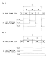
- FIG. 4 illustrates one example of the operation of the display 1 in the case C 1 , in which (A) schematically illustrates an example of the image signal SIG 4 and (B) illustrates examples of waveforms of the light emission control signals CTLR, CTLG, and CTLB.
- PR indicates the one-frame luminance information IR (the red image PR)
- PG indicates the one-frame luminance information IG (the green image PG)
- PB indicates the one-frame luminance information IB (the blue image PB).
- a high level indicates light emission and a low level indicates light extinction in each of the light emission control signals CTLR, CTLG, and CTLB.
- the one-frame luminance information IR (the red image PR) is supplied to the liquid crystal display section 20 ((A) of FIG. 4 ), and the high-level light emission control signal CTLR and the low-level light emission control signals CTLG and CTLB are supplied to the backlight 30 ((B) of FIG. 4 ) in the first subfield SF in the one-frame period.
- the liquid crystal display section 20 displays the red image PR and the light emitting section 30 R of the backlight 30 emits the red light.
- the one-frame luminance information IG (the green image PG) is supplied to the liquid crystal display section 20 ((A) of FIG.
- the liquid crystal display section 20 displays the green image PG and the light emitting section 30 G of the backlight 30 emits the green light.
- the one-frame luminance information IB (the blue image PB) is supplied to the liquid crystal display section 20 ((A) of FIG. 4 ), and the high-level light emission control signal CTLB and the low-level light emission control signals CTLR and CTLG are supplied to the backlight 30 ((B) of FIG. 4 ) in the third subfield SF.
- the liquid crystal display section 20 displays the blue image PB and the light emitting section 30 B of the backlight 30 emits the blue light.
- the display 1 displays a colored image by displaying the red image PR, the green image PG, and the blue image PB in time division in this way.
- the analysis section 15 determines that only the red image PR and the green image PG are to be displayed and informs the control section 17 of this determination using the color information CI.
- the control section 17 sets two subfields SF in the one-frame period and generates the memory control signal SMEM and the backlight control signal SBL.
- the memory control section 13 reads out the one-frame luminance information IR (the red image PR) and the one-frame luminance information IG (the green image PG) from the memory 9 in the respective two subfields SF on the basis of the memory control signal SMEM, and outputs the information so read-out as the image signal SIG 3 . That is, the memory control section 13 does not read out the one-frame luminance information IB (the blue image PB) from the memory 9 . Then, the signal correction section 14 performs correction on the image signal SIG 3 and generates the image signal SIG 4 . In addition, the backlight control section 18 generates the light emission control signals CTLR, CTLG, and CTLB on the basis of the backlight control signal SBL.
- FIG. 5 illustrates one example of the operation of the display 1 in the case C 2 , in which (A) schematically illustrates one example of the image signal SIG 4 and (B) illustrates examples of the waveforms of the light emission control signals CTLR, CTLG, and CTLB.
- the one-frame luminance information IR (the red image PR) is supplied to the liquid crystal display section 20 ((A) of FIG. 5 ) and the high-level light emission control signal CTLR and the low-level light emission control signals CTLG and CTLB are supplied to the backlight 30 ((B) of FIG. 5 ) in the first subfield SF in the one-frame period.
- the liquid crystal display section 20 displays the red image PR and the light emitting section 30 R of the backlight 30 emits the red light.
- the one-frame luminance information IG (the green image PG) is supplied to the liquid crystal display section 20 ((A) of FIG. 5 ) and the high-level light emission control signal CTLG and the low-level light emission control signals CTLR and CTLB are supplied to the backlight 30 ((B) of FIG. 5 ) in the second subfield SF.
- the liquid crystal display section 20 displays the green image PG and the light emitting section 30 G of the backlight 30 emits the green light.
- the display 1 displays a yellow image by displaying the red image PR and the green image PG, in time division in this way.
- the analysis section 15 determines that display of the blue image PB is not necessary and the display 1 displays the two images (the red image PR and the green image PG) excluding the blue image PB in time division.
- the analysis section 15 determines that only the blue image PB is to be displayed and informs the control section 17 of this determination using the color information CI.
- the control section 17 sets one subfield SF in the one-frame period and generates the memory control signal SMEM and the backlight control signal SBL.
- the memory control section 13 reads out the one-frame luminance information IB (the blue image PB) from the memory 9 in the one subfield SF and outputs the information so read-out as the image signal SIG 3 . That is, the memory control section 13 does not read out the one-frame luminance information IR (the red image PR) and the one-frame luminance information IG (the green image PG) from the memory 9 . Then, the signal correction section 14 performs correction on the image signal SIG 3 and generates the image signal SIG 4 . In addition, the backlight control section 18 generates the light emission control signals CTLR, CTLG, and CTLB on the basis of the backlight control signal SBL.
- FIG. 6 illustrates one example of the operation of the display 1 in the case C 3 , in which (A) schematically illustrates one example of the image signal SIG 4 and (B) illustrates examples of the waveforms of the light emission control signals CTLR, CTLG, and CTLB.
- the one-frame luminance information IB (the blue image PB) is supplied to the liquid crystal display section 20 ((A) of FIG. 6 ) and the high-level light emission control signal CTLB and the low-level light emission control signals CTLR and CTLG are supplied to the backlight 30 ((B) of FIG. 6 ) in the one-frame period (the subfield SF).
- the liquid crystal display section 20 displays the blue image PB and the light emitting section 30 B of the backlight 30 emits the blue light.
- the display 1 displays only the blue image PB in this way. That is, since all of the luminance levels of each of the pieces of one-frame luminance information IR and IG are less than the threshold value Lth, the analysis section 15 determines that display of the red image PR and the green image PG is not necessary and the display 1 displays only the blue image PB.
- the analysis section 15 determines the image(s) to be displayed out of the red image PR, the green image PG, and the blue image PB in this way. Then, the control section 17 dynamically changes the number of the subfields SF in the one-frame period in accordance with the number of images to be displayed out of the red image PR, the green image PG, and the blue image PB on the basis of a result of the above-mentioned determination, and controls the display 1 so as to display the images in the respective subfields SF.
- the display 1 whether the image that has been supplied is the usual image (for example, the case C 1 ) or the image that only one or two of the red light, the green light, and the blue light is/are used as in the case of the so-called blue screen (for example, the case C 2 or C 3 ) is determined, and in the latter case, the number of the subfields SF in the one-frame period is reduced.
- the display luminance of the display 1 it is possible to increase the display luminance of the display 1 and it is also possible to reduce the power consumption when the image that only one or two of the red light, the green light, and the blue light is/are used is to be displayed as described below in comparison with a comparative example.
- the display 1 R is adapted to constantly set three subfields SF in the one-frame period.
- FIG. 7 illustrates one configuration example of the display 1 R according to the comparative example.
- the display 1 R includes a control section 13 R.
- the control section 13 R is adapted to control the operations of writing and reading out the pieces of luminance information IR, IG, and/or IB into and from the memory 9 on the basis of the image signals SR 2 , SG 2 , and SB 2 , and the synchronous signal Sync 2 , and to output the read-out pieces of luminance information IR, IG, and/or IB as the image signal SIG 3 .
- control section 13 R constantly sets the three subfields SF in the one-frame period, reads out the one-frame luminance information IR (the red image PR), the one-frame luminance information IG (the green image PG), and the one-frame luminance information IB (the blue image PB) in the respective three subfields SF, and outputs the read-out information as the image signal SIG 3 .
- control section 13 R also has a function of generating the light emission control signals CTLR, CTLG, and CTLB that synchronize with display of the red image PR, the green image PG, and the blue image PB.
- FIG. 8 illustrates one example of the operation of the display 1 R in the case C 2
- FIG. 9 illustrates one example of the operation of the display 1 R in the case C 3
- (A) schematically illustrates one example of the image signal SIG 4
- (B) illustrates examples of the waveforms of the light emission control signals CTLR, CTLG, and CTLB.
- CTLR light emission control signals
- CTLG light emission control signals
- the liquid crystal display section 20 displays the red image PR and the light emitting section 30 R of the backlight 30 emits the red light in the first subfield SF in the one-frame period
- the liquid crystal display section 20 displays the green image PG and the light emitting section 30 G of the backlight 30 emits the green light in the second subfield SF
- the liquid crystal display section 20 displays the blue image PB and the light emitting section 30 B of the backlight 30 emits the blue light in the third subfield SF.
- the blue image PB is displayed as a near black blue image. Therefore, in the example in FIG. 8 , although the light emitting section 30 B emits light, the display 1 R performs black display and therefore a period that hardly contributes to display is created in the third subfield SF. In the case C 3 , since all of the luminance levels of each of the pieces of one-frame luminance information IR and IG are less than the threshold value Lth, both of the red image PR and the green image PG are displayed as near black images similarly. Therefore, in the example in FIG. 9 , although the light emitting sections 30 R and 30 G emit light, the display 1 R performs the black display and therefore the period that hardly contributes to display is created in each of the first and second subfields SF.
- the display 1 R according to the comparative example Since in the display 1 R according to the comparative example, the number of subfields SF in the one-frame period has been fixed to three as described above, the period that hardly contributes to display is created when the image in which only one or two of the red light, the green light, and the blue light is/are used is to be displayed as in the case of the so-called blue screen. In such a period, the power consumption may possibly be wasted due to light emission of the backlight 30 (the light emitting sections 30 R, 30 G, and 30 B).
- the display 1 is configured such that the image(s) to be displayed out of the red image PR, the green image PG, and the blue image PB is/are determined and the number of subfields SF in the one-frame period is dynamically changed depending on the image(s) to be displayed.
- the display luminance of the display 1 since it is possible to omit the period that does not contribute to display in the display 1 , it is possible to increase the display luminance of the display 1 and it is also possible to suppress waste of the power consumption. That is, for example, as to the case C 2 , the example in FIG.
- the embodiment may correspond to an example in which the light emission period (the third subfield SF) of the light emitting section 30 B is omitted and the light emission periods (the first and second subfields SF) of the light emitting sections 30 R and 30 G are lengthened in FIG. 8 according to the comparative example.
- the light emission period (the third subfield SF) of the light emitting section 30 B is omitted and the light emission periods (the first and second subfields SF) of the light emitting sections 30 R and 30 G are lengthened in FIG. 8 according to the comparative example.
- the 6 according to the present embodiment may correspond to an example in which the light emission periods (the first and second subfields SF) of the light emitting sections 30 R and 30 G are omitted and the light emission period (the third subfield SF) of the light emitting section 30 B is lengthened in FIG. 9 according to the comparative example in the same way.
- the light emission periods (the first and second subfields SF) of the light emitting sections 30 R and 30 G are omitted and the light emission period (the third subfield SF) of the light emitting section 30 B is lengthened in FIG. 9 according to the comparative example in the same way.
- the liquid crystal display section 20 since in the display 1 R according to the comparative example, the three subfields are constantly set in the one-frame period, it is necessary for the liquid crystal display section 20 to perform scan driving three times in the one-frame period constantly and therefore the power consumption may possibly be increased.
- the number of subfields SF in the one-frame period is dynamically changed, it is possible to reduce the number of times of performing scan driving by the liquid crystal display section 20 depending on the image(s) to be displayed and therefore it is possible to reduce the power consumption.
- the number of subfields SF in the one-frame period is dynamically changed as described above, it is possible to increase the display luminance and the image quality of the display and it is also possible to reduce the power consumption when such display that only one or two of the red light, the green light, and the blue light is/are used is to be performed as in the case of the blue screen.
- the backlight control section 18 may be configured to set a start timing and a finish timing of each pulse (a pulse phase and a pulse width) in each of the light emission control signals CTLR, CTLG, and CTLB, for example, as illustrated in FIG. 10 .
- the timings are set such that the pulse widths of the light emission control signals CTLR, CTLG, and CTLB are made different from one another.
- each of the light emitting sections 30 R, 30 G, and 30 B emit light at a timing that liquid crystal response and so forth of the liquid crystal display section 20 are taken into account, by configuring so as to set the start timing and the finish timing of each pulse as described above.
- one subfield SF has been set in the one-frame period when one of the red image PR, the green image PG, and the blue image PB is to be displayed (for example, the case C 3 ), the present disclosure is not limited to this configuration.
- a plurality (in this example, three) of the subfields SF may be set in the one-frame period and the same image (in this example, the blue image PB) may be repetitively displayed.
- scan driving is performed a plurality of times (in this example, three times) in the one-frame period in the liquid crystal display section 20 , it is possible to reduce degradation of image quality caused by leakage in a transistor of the pixel Pix.
- a configuration that allows setting of the start timing and the finish timing (the pulse phase and the pulse width) of each pulse in each of the light emission control signals CTLR, CTLG, and CTLB may be possible as illustrated in FIG. 12 .
- the two subfields have been set in the one-frame period when two of the red image PR, the green image PG, and the blue image PB are to be displayed (for example, the case C 2 ), the present disclosure is not limited to this configuration.
- three or more subfields SF may be set in the one-frame period or one subfield SF may be set in the one-frame period.
- the present modification example will be described in detail by giving several examples thereof.
- the display 2 is adapted to set four subfields SF in the one-frame period in the case C 2 .
- FIG. 13 illustrates one example of the operation of the display 2 in the case C 2 , in which (A) schematically illustrates one example of the image signal SIG 4 and (B) illustrates examples of the waveforms of the light emission control signals CTLR, CTLG, and CTLB.
- the display 2 sets the four subfields SF in the one-frame period in the case C 2 .
- the one-frame luminance information IR (the red image PR) is supplied to the liquid crystal display section 20 ((A) of FIG. 13 ) and the high-level light emission control signal CTLR and the low-level light emission control signals CTLG and CTLB are supplied to the backlight 30 ((B) of FIG. 13 ) in the first subfield SF.
- the liquid crystal display section 20 displays the red image PR and the light emitting section 30 R of the backlight 30 emits the red light.
- the one-frame luminance information IG (the green image PG) is supplied to the liquid crystal display section 20 ((A) of FIG. 13 ) and the high-level light emission control signal CTLG and the low-level light emission control signals CTLR and CTLB are supplied to the backlight 30 ((B) of FIG. 13 ) in the second subfield SF.
- the liquid crystal display section 20 displays the green image PG and the light emitting section 30 G of the backlight 30 emits the green light.
- the one-frame luminance information IR (the red image PR) which is the same as the information in the first subfield SF is again supplied to the liquid crystal display section 20 ((A) of FIG. 13 ) and the high-level light emission control signal CTLR and the low-level light emission control signals CTLG and CTLB are supplied to the backlight 30 ((B) of FIG. 13 ) in the third subfield SF.
- the liquid crystal display section 20 displays the red image PR and the light emitting section 30 R of the backlight 30 emits the red light.
- the one-frame luminance information IG (the green image PG) which is the same as the information in the second subfield SF is again supplied to the liquid crystal display section 20 ((A) of FIG.
- the liquid crystal display section 20 displays the green image PG and the light emitting section 30 G of the backlight 30 emits the green light.
- the display 2 displays the red image PR and the green image PG two times per image in time division in the one-frame period in this way. For example, it is possible to reduce the probability that a viewer feels as if the image quality has been reduced when the viewer has not viewed a display screen for a very short period of time by blinking eyes as described below in comparison with the display 1 R according to the comparative example.
- FIG. 14 illustrates one example of the operation of the display 1 R according to the comparative example in the case C 2
- FIG. 15 illustrates one example of the operation of the display 2 according to the modification example in the case C 2
- (A) schematically illustrates one example of the image signal SIG 4
- (B) illustrates examples of the waveforms of the light emission control signals CTLR, CTLG, and CTLB.
- the viewer when the viewer has not observed the display screen of the display 1 R in a very short period PV from timings t 1 to t 2 , the viewer may possibly see a color which is different from the original color immediately before the timing t 1 and immediately after the timing t 2 as illustrated in FIG. 14 . Specifically, in this example, the viewer may possibly recognize that a somewhat reddish image is displayed on the display screen immediately before the timing t 1 and may possibly recognize that a somewhat greenish image is displayed on the display screen immediately after the timing t 2 . In the display 1 R according to the comparative example, the viewer may possibly feel that the image quality has been reduced due to occurrence of so-called “color breakup” as described above.
- the display 2 according to the present modification example it is possible for the viewer to see the color which is almost the same as the original color even immediately before the timing t 1 and immediately after the timing t 2 as illustrated in FIG. 15 . That is, since in the display 2 , many subfields SF are set in the one-frame period, it is possible to reduce the possibility of occurrence of the color breakup and therefore it is possible to increase the image quality.
- the display 3 is adapted to set one subfield SF in the one-frame period and to make two of the light emitting sections 30 R, 30 G, and 30 B emit light.
- FIG. 16 illustrates one configuration example of the display 3 according to the present modification example.
- the display 3 includes a control section 47 and a signal generation section 43 .
- the control section 47 is adapted to set one or the plurality of subfields SF in the one-frame period on the basis of the color information CI and to control the display 3 so as to display each image in each of the subfields SF as in the control section 17 according to the above-mentioned embodiment.
- the control section 47 sets one subfield SF in the one-frame period.
- the control section 47 generates a control signal SSIG indicating that the two images correspond to which images of the red image PR, the green image PG, and the blue image PB.
- the control section 47 operates in the same way as the control section 17 .
- the signal generation section 43 is adapted to generate an image signal S 10 and a synchronous signal Sync 10 that synchronizes with the image signal S 10 on the basis of the image signals SR 2 , SG 2 , and SB 2 , the synchronous signal Sync 2 , and the control signal SSIG.
- the signal generation section 43 when two of the red image PR, the green image PG, and the blue image PB are to be displayed (for example, the case C 2 ), the signal generation section 43 generates an image of a combination color of those two images on the basis of the control signal SSIG and outputs the image so generated as the image signal S 10 .
- the signal generation section 43 may generate a yellow image PY and may output the image signal S 10 that includes luminance information IY of yellow (Y).
- the signal generation section 43 may generate a cyan image PC and may output the image signal S 10 that includes luminance information IC of cyan (C).
- the signal generation section 43 may generate a magenta image PM and may output the image signal S 10 that includes luminance information IM of magenta (M).
- RGB/YUV conversion may be performed on the basis of the pieces of luminance information IR, IG, and IB included in the image signals SR 2 , SG 2 , and SB 2 and a Y component in the YUV signal so converted may be used as the pieces of luminance information IY, IC, and IM.
- the signal generation section 43 may not generate any image and may output the image signals SR 2 , SG 2 , and SB 2 as the image signal S 10 as they are.
- the control section 47 may set one subfield SF in the one-frame period and may generate the control signal SSIG owing to the above-mentioned configuration.
- the signal generation section 43 may generate an image of a combination color of these two images and may output the image as the image signal S 10 on the basis of the control signal SSIG.
- the signal generation section 43 corresponds to one specific example of a “luminance information generation section” in one embodiment of the present disclosure.
- FIG. 17 illustrates one example of the operation of the display 3 in the case C 2 , in which (A) schematically illustrates one example of the image signal SIG 4 and (B) illustrates examples of the waveforms of the light emission control signals CTLR, CTLG, and CTLB.
- the analysis section 15 determines that two images, i.e., the red image PR and the green image PG are to be displayed
- the signal generation section 43 generates the yellow image PY.
- luminance information that configures the yellow image PY is supplied to the liquid crystal display section 20 ((A) of FIG. 17 ) and the high-level light emission signals CTLR and CTLG and the low-level light emission control signal CTLB are supplied to the backlight 30 ((B) of FIG. 17 ) in the one-frame period (the subfield SF).
- the liquid crystal display section displays the yellow image PY and the backlight 30 emits yellow light as red and green combination light.
- the light emission control signals CTLR, CTLG, and CTLB have been made to be maintained at the high levels or the low levels over the period of the subfield SF
- the present disclosure is not limited to this configuration.
- the start timing and the finish timing (the pulse phase and the pulse width) of each pulse in each of the light emission control signals CTLR, CTLG, and CTLB may be changed, for example, as illustrated in FIG. 18 .
- this combination ratio may be changed, for example, using the pieces of luminance information IR, IG, and IB.
- the backlight 30 it is possible for the backlight 30 to emit light in a color according to the pieces of luminance information IR, IG, and IB.
- one or more of the light emission control signals CTLR, CTLG, and CTLB may be configured by a plurality of pulses as illustrated in FIG. 19 . In this case, it is possible to reduce the probability that color breakup occurs and therefore it is possible to increase the image quality as in the case of the display 2 according to the above-mentioned present modification example.
- a color of the light that the backlight 30 emits may be adjusted by changing the emission luminances of the respective light emitting sections 30 R, 30 G, and 30 B by changing the signal levels of the light emission control signals CTLR, CTLG, and CTLB, for example, as illustrated in FIG. 20 .
- the emission luminance of the light emitting section 30 G is made lower than the emission luminance of the light emitting section 30 R by supplying a voltage VH to the light emitting section 30 R and supplying a voltage VM which is lower than the voltage VH to the light emitting section 30 G.
- the emission luminances of the light emitting sections 30 R, 30 G, and 30 B have been adjusted by supplying voltages, the present disclosure is not limited to this. Alternatively, the emission luminances may be adjusted, for example, by supplying currents to the light emitting sections.
- one subfield SF has been set in the one-frame period and two of the light emitting sections 30 R, 30 G, and 30 B have been made to emit light in the case C 2
- the present disclosure is not limited to this.
- one subfield SF may be set in the one-frame period and all of the light emitting sections 30 R, 30 G, and 30 B may be made to emit light in the case C 1 .
- the analysis section 15 has determined the image(s) to be displayed out of the red image PR, the green image PG, and the blue image PB on the basis of the image signals SR 2 , SG 2 , and SB 2 and the synchronous signal Sync 2 which are the output signals from the color correction section 12 , the present disclosure is not limited to this configuration.
- the analysis section 15 may perform this processing (image determination) on the basis of the image signals SR 1 , SG 1 , and SB 1 and the synchronous signal Sync 1 which are the input signals into the color correction section 12 .
- the display 1 includes the analysis section 15
- the present disclosure is not limited to this configuration.
- the analysis section 15 may not be included when it is possible to supply the color signal (the color information) CI from the outside, for example, as in a display 1 B illustrated in FIG. 22 .
- a circuit that is disposed at a stage preceding the display 1 B performs analysis of the image to be displayed in the display 1 B and outputs the color signal CI
- application of the present modification example is possible.
- the image signals and the color signal CI have been made to be separately supplied, the present disclosure is not limited to this configuration and they may be supplied, for example, in the form of one time-division-multiplexed signal.
- an operation mode setting section 49 that sets one of a plurality of operation modes including a normal display mode M 1 and a monochromatic display mode M 2 may be included so as to make the operation mode setting section 49 generate the color information CI.
- the operation mode setting section 49 may generate the color information CI indicating that all of the red image PR, the green image PG, and the blue image PB are to be displayed and the display 1 C may operate in a manner as in the case C 1 .
- the operation mode setting section 49 may generate the color information CI indicating, for example, that only the blue image PB is to be displayed and the display 1 C may operate in a manner as in the case C 3 .
- the display 1 C may operate in a manner as in the case C 3 .
- the color correction section 12 has been provided at the upstream of the memory control section 13 , the present disclosure is not limited to this configuration.
- a color correction section 12 D may be provided at the downstream of the memory control section 13 , for example, as in a display 1 D illustrated in FIG. 24 .
- the color correction section 12 D performs color-related correction on the basis of the image signal SIG 3 and the synchronous signal Sync 3 output from the memory control section 13 .
- the color correction section 12 D generates an image signal SIG 11 by performing the correction, generates a synchronous signal Sync 11 that synchronizes with the image signal SIG 11 , and supplies the generated signals to the signal correction section 14 .
- the signal correction section 14 has been provided at the downstream of the memory control section 13 , the present disclosure is not limited to this configuration. Alternatively, the signal correction section 14 may be provided, for example, at the upstream of the memory control section 13 . In the following, a display 1 E according to the present modification example will be described.
- FIG. 25 illustrates one configuration example of the display 1 E.
- the display 1 E includes a control section 17 E and a signal correction section 14 E.
- the control section 17 E has a function which is the same as that of the control section 17 according to the above-mentioned embodiment, and is configured to generate subfield information INFO indicating which one of the red image PR, the green image PG, and the blue image PB is made in one-to-one correspondence with which subfield SF and to supply the information INFO to the signal correction section 14 E.
- the signal correction section 14 E performs correction on the signal received on the basis of the image signals SR 2 , SG 2 , and SB 2 and the synchronous signal Sync 2 output from the color correction section 12 .
- the signal correction section 14 E performs correction based on the pieces of luminance information IR, IG, and IB in the plurality of adjacent subfields SF in the same way as the signal correction section 14 . In that case, the signal correction section 14 E performs this correction on the basis of the subfield information INFO. Then, the signal correction section 14 E generates image signals SR 12 , SG 12 , and SB 12 by performing the above-mentioned correction and a synchronous signal Sync 12 that synchronizes with the image signals SR 12 , SG 12 , and SB 12 , and supplies the generated signals to the memory control section 13 and the analysis section 15 .
- the RGB signal has been made to be input into the display 1
- the present disclosure is not limited to this configuration, and a signal of any other format may be input into the display.
- a display 1 F into which a YUV signal is input will be described.
- FIG. 26 illustrates one configuration example of the display 1 F.
- the display 1 F includes an image input section 11 F and a signal conversion section 40 F.
- the image input section 11 F is adapted to output image signals which are in the form of the YUV signal as image signals SY, SU, and SV, and a synchronous signal Sync 0 that synchronizes with the image signals SY, SU, and SV.
- the signal conversion section 40 F is adapted to convert (the YUV/RGB conversion) the YUV signal into an RGB signal.
- the signal conversion section 40 F performs the YUV/RGB conversion on the basis of the image signals SY, SU, and SV that configure the YUV signal and the synchronous signal Sync 0 , and generates the image signals SR 1 , SG 1 , and SB 1 that configure the RGB signal and the synchronous signal Sync 1 .
- the signal conversion section 40 F corresponds to one specific example of a “conversion section” in one embodiment of the present disclosure. It is to be noted that although in this example, the signal conversion section 40 F has been provided at the upstream of the color correction section 12 , the present disclosure is not limited to this, and the signal conversion section 40 F may be provided at any location as long as it is provided at the upstream of the memory control section 13 .
- the memory control section 13 has been configured to write the pieces of one-frame luminance information IR, IG, and IB included in the image signals SR 2 , SG 2 , and SB 2 into the memory 9 and to read out only the luminance information to be displayed among them from the memory 9 , the present disclosure is not limited to this configuration.
- the memory control section 13 may be configured to write only the luminance information to be displayed into the memory 9 .
- the emission luminances of the light emitting sections 30 R, 30 G, and 30 B have been fixed regardless of the number of the subfields SF in the one-frame period, the present disclosure is not limited to this configuration.
- the emission luminances of the light emitting sections 30 R, 30 G, and 30 B may be set to be reduced, for example, as the number of the subfields SF is reduced.
- the possibility that the viewer feels unnaturalness due to a rapid increase in display luminance is reduced.
- FIG. 27 illustrates one example of the outside appearance of a television apparatus to which the display according to any of the above-mentioned embodiment and modification examples is applied.
- the television apparatus may include, for example, an image display screen section 510 including a front panel 511 and a filter glass 512 , and the image display screen section 510 is configured by the display according to any of the above-mentioned embodiment and modification examples.
- the backlight 30 includes the three light emitting sections 30 R, 30 G, and 30 B
- the present disclosure is not limited to this configuration.
- the backlight may include two or less, or four or more light emitting sections that emit light of different colors from one another, and/or may include a light emitting section or sections that emit(s) light of a color or colors other than red, green, and blue.
- the backlight 30 includes the light emitting sections 30 R, 30 G, and 30 B
- the present disclosure is not limited to this configuration.
- the backlight may include light emitting sections 30 AR, 30 AG, and 30 AB on its upper half part and light emitting sections 30 BR, 30 BG, and 30 BB on its lower half part as in, for example, a backlight 30 G illustrated in FIG. 28 .
- the light emitting sections 30 AR, 30 AG, and 30 AB are adapted to respectively emit the red (R) light, the green (G) light, and the blue (B) light on the basis of light emission control signals CTLAR, CTLAG, and CTLAB
- the light emitting sections 30 BR, 30 BG, and 30 BB are adapted to respectively emit the red (R) light, the green (G) light, and the blue (B) light on the basis of light emission control signals CTLBR, CTLBG, and CTLBB in the same way.
- FIG. 29 schematically illustrates one example of a projector 60 using the DLP technology.
- the projector 60 includes a light source system 61 , a prism 63 , a DMD (Digital Minor Device) 64 , and a projection lens 65 .
- the red (R) light, the green (G) light, and the blue (B) light are radiated in time division from the light source system 61 .
- the light of each color is incident upon the DMD 64 that includes a plurality of movable micro-mirrors via the prism 63 .
- the light reflected from the DMD 64 is incident upon the projection lens 65 again via the prism 63 and projected onto the screen.
- a display device configured to display at least one image, the display device comprising:
- At least one light emitter configured to emit a plurality of colored light beams, each of the plurality of colored light beams being a respective color different than the others;
- a light emission controller configured to determine, based on at least one characteristic of the at least one image, one or more light beams of the plurality of colored light beams to emit in a frame period corresponding to the at least one image.
- the at least one characteristic of the at least one image comprises luminance value information related to color components of the at least one image corresponding to the respective colors of the plurality of colored light beams.
- a display section configured to display the at least one image by transmitting or reflecting light from the at least one light emitter.
- a display controller configured to drive the display section based on the luminance value information.
- a memory configured to store the luminance information, wherein:
- the display controller is configured to:
- the light emission controller is further configured to extend a light emission time of the one or more light beams of the plurality of colored light beams to emit in the frame period corresponding to the at least one image.
- the light emission controller is further configured to control a light emission start time and/or a light emission finish time of the one or more light beams of the plurality of colored light beams to emit in the frame period corresponding to the at least one image.
- the display device of (1) further comprising a converter configured to convert a signal other than an RGB signal into an RGB signal.
- a light emission controller configured to control at least one light emitter, the light emission controller comprising:
- an analyzer configured to:
- each of the plurality of image signals corresponding to a respective color
- controller configured to control the at least one light emitter based on the determination of the analyzer.
- a light emitting device comprising:
- each of the plurality of light emitters configured to emit light of a different color
- a light emission controller configured to:
- each of the image signals corresponding to a respective one of the plurality of colors
- CTLR CTLG
- CTLB Light emission control signal
Landscapes
- Engineering & Computer Science (AREA)
- Physics & Mathematics (AREA)
- Computer Hardware Design (AREA)
- General Physics & Mathematics (AREA)
- Theoretical Computer Science (AREA)
- Multimedia (AREA)
- Chemical & Material Sciences (AREA)
- Crystallography & Structural Chemistry (AREA)
- Control Of Indicators Other Than Cathode Ray Tubes (AREA)
- Liquid Crystal Display Device Control (AREA)
- Liquid Crystal (AREA)
Applications Claiming Priority (3)
| Application Number | Priority Date | Filing Date | Title |
|---|---|---|---|
| JP2013132443A JP6367529B2 (ja) | 2013-06-25 | 2013-06-25 | 表示装置、表示制御方法、表示制御装置、および電子機器 |
| JP2013-132443 | 2013-06-25 | ||
| PCT/JP2014/003229 WO2014208046A1 (en) | 2013-06-25 | 2014-06-17 | Display, display control method, display control device, and electronic apparatus |
Publications (2)
| Publication Number | Publication Date |
|---|---|
| US20150235620A1 US20150235620A1 (en) | 2015-08-20 |
| US9899000B2 true US9899000B2 (en) | 2018-02-20 |
Family
ID=51225866
Family Applications (1)
| Application Number | Title | Priority Date | Filing Date |
|---|---|---|---|
| US14/422,103 Expired - Fee Related US9899000B2 (en) | 2013-06-25 | 2014-06-17 | Display, display control method, display control device, and electronic apparatus |
Country Status (5)
| Country | Link |
|---|---|
| US (1) | US9899000B2 (enExample) |
| EP (1) | EP3014603B1 (enExample) |
| JP (1) | JP6367529B2 (enExample) |
| CN (1) | CN104541321B (enExample) |
| WO (1) | WO2014208046A1 (enExample) |
Cited By (10)
| Publication number | Priority date | Publication date | Assignee | Title |
|---|---|---|---|---|
| US10477174B2 (en) | 2014-02-10 | 2019-11-12 | Sony Corporation | Image display device and display apparatus |
| US10527859B2 (en) | 2013-04-11 | 2020-01-07 | Sony Corporation | Image display device and display apparatus |
| US10534172B2 (en) | 2013-07-16 | 2020-01-14 | Sony Corporation | Display apparatus |
| US10540822B2 (en) | 2012-05-09 | 2020-01-21 | Sony Corporation | Display instrument and image display method |
| US10613329B2 (en) | 2013-02-20 | 2020-04-07 | Sony Corporation | Display device with transmissivity controlled based on quantity of light |
| US10642040B2 (en) | 2014-03-17 | 2020-05-05 | Sony Corporation | Display apparatus and optical apparatus |
| US10663736B2 (en) | 2013-04-11 | 2020-05-26 | Sony Corporation | Image display device and display apparatus |
| US10942355B2 (en) * | 2018-01-22 | 2021-03-09 | Facebook Technologies, Llc | Systems, devices, and methods for tiled multi-monochromatic displays |
| US11150478B2 (en) | 2014-02-10 | 2021-10-19 | Sony Corporation | Head mounted image display device and display device |
| US11600226B2 (en) * | 2020-07-30 | 2023-03-07 | Samsung Display Co., Ltd. | Display device |
Families Citing this family (13)
| Publication number | Priority date | Publication date | Assignee | Title |
|---|---|---|---|---|
| JP5499854B2 (ja) | 2010-04-08 | 2014-05-21 | ソニー株式会社 | 頭部装着型ディスプレイにおける光学的位置調整方法 |
| JP5434848B2 (ja) | 2010-08-18 | 2014-03-05 | ソニー株式会社 | 表示装置 |
| JP5780129B2 (ja) | 2011-11-22 | 2015-09-16 | ソニー株式会社 | 光ビーム伸長装置、画像表示装置及び光学装置 |
| JP5879973B2 (ja) | 2011-11-30 | 2016-03-08 | ソニー株式会社 | 光反射部材、光ビーム伸長装置、画像表示装置及び光学装置 |
| JP6003903B2 (ja) | 2012-01-24 | 2016-10-05 | ソニー株式会社 | 表示装置 |
| CN104204905B (zh) | 2013-01-10 | 2016-11-23 | 索尼公司 | 图像显示设备、图像生成装置以及透射式空间光调制装置 |
| EP3439293A3 (en) | 2013-07-16 | 2019-05-01 | Sony Corporation | Display apparatus |
| JP2015184561A (ja) | 2014-03-25 | 2015-10-22 | ソニー株式会社 | 導光装置、画像表示装置及び表示装置 |
| JP2015184560A (ja) | 2014-03-25 | 2015-10-22 | ソニー株式会社 | 導光装置、画像表示装置及び表示装置 |
| KR20160147122A (ko) * | 2015-06-11 | 2016-12-22 | 삼성디스플레이 주식회사 | 표시 장치 및 그 제어 방법 |
| US20180301098A1 (en) * | 2015-08-18 | 2018-10-18 | Sharp Kabushiki Kaisha | Display device and method for driving same |
| US11259384B2 (en) * | 2020-05-09 | 2022-02-22 | Tcl China Star Optoelectronics Technology Co., Ltd. | Backlight unit and control method thereof, and liquid crystal display device |
| TWI889141B (zh) * | 2024-01-15 | 2025-07-01 | 友達光電股份有限公司 | 顯示面板 |
Citations (56)
| Publication number | Priority date | Publication date | Assignee | Title |
|---|---|---|---|---|
| JPH09244166A (ja) | 1996-03-08 | 1997-09-19 | Nikon Corp | 立体表示装置 |
| EP0997868A1 (en) | 1998-10-30 | 2000-05-03 | Sel Semiconductor Energy Laboratory Co., Ltd. | Field sequential liquid crystal display device and driving method thereof, and head mounted display |
| JP2000199886A (ja) | 1998-10-30 | 2000-07-18 | Semiconductor Energy Lab Co Ltd | フィ―ルドシ―ケンシャル液晶表示装置およびその駆動方法ならびにヘッドマウントディスプレイ |
| JP2001203956A (ja) | 2000-01-24 | 2001-07-27 | Mixed Reality Systems Laboratory Inc | ヘッドマウントディスプレイ装置及び情報処理システム |
| US20020030636A1 (en) | 2000-06-26 | 2002-03-14 | Richards Angus Duncan | Virtual reality display device |
| JP2003248462A (ja) | 2002-02-22 | 2003-09-05 | Fujitsu Ltd | 画像表示装置及び画像表示方法 |
| EP1379082A1 (en) | 2002-07-04 | 2004-01-07 | Koninklijke Philips Electronics N.V. | Display apparatus |
| JP2005521099A (ja) | 2002-03-21 | 2005-07-14 | ラマス リミテッド | 光導体光学装置 |
| WO2006061927A1 (ja) | 2004-12-06 | 2006-06-15 | Nikon Corporation | 画像表示光学系、画像表示装置、照明光学系、及び液晶表示装置 |
| JP2006162767A (ja) | 2004-12-03 | 2006-06-22 | Nikon Corp | 画像表示光学系及び画像表示装置 |
| CN1940610A (zh) | 2005-09-29 | 2007-04-04 | 索尼株式会社 | 光学器件与图像显示设备 |
| CN1957269A (zh) | 2004-05-17 | 2007-05-02 | 株式会社尼康 | 光学元件、合成器光学系统以及图像显示单元 |
| US20070152945A1 (en) | 2005-12-30 | 2007-07-05 | Lg Philips Lcd Co., Ltd. | Liquid crystal display of field sequential color type and method for driving the same |
| US20070176943A1 (en) | 2006-02-02 | 2007-08-02 | Samsung Electronics Co., Ltd. | Field sequential image display apparatus and method of driving the same |
| US20070205969A1 (en) * | 2005-02-23 | 2007-09-06 | Pixtronix, Incorporated | Direct-view MEMS display devices and methods for generating images thereon |
| US20070229444A1 (en) * | 2006-03-29 | 2007-10-04 | Chun-Ting Liu | Liquid crystal display, method for displaying color images, and method for controlling light sources of an lcd panel |
| JP2008129302A (ja) | 2006-11-21 | 2008-06-05 | Renesas Technology Corp | 表示装置用駆動回路 |
| US20080143736A1 (en) * | 2006-12-14 | 2008-06-19 | Texas Instruments Incorporated | System and method for dynamically altering a color gamut |
| JP2008225292A (ja) | 2007-03-15 | 2008-09-25 | Stanley Electric Co Ltd | 液晶表示素子、それを用いた投射型表示装置およびそれぞれの駆動方法 |
| JP2009020384A (ja) | 2007-07-13 | 2009-01-29 | Seiko Epson Corp | 電気光学装置、その制御方法および電子機器 |
| US20090058794A1 (en) * | 2007-08-31 | 2009-03-05 | Stanley Electric Co., Ltd | Liquid crystal display device with improved display luminance |
| US20090079769A1 (en) | 2007-09-25 | 2009-03-26 | Seiko Epson Corporation | Driving method, driving circuit, electro-optical device, and electronic apparatus |
| JP2009134156A (ja) | 2007-11-30 | 2009-06-18 | Univ Of Electro-Communications | 画像表示の信号処理方法及び画像表示装置 |
| US20090295839A1 (en) * | 2008-05-20 | 2009-12-03 | Sony Corporation | Display device, drive method therefor, and electronic apparatus |
| US20100103078A1 (en) | 2008-10-23 | 2010-04-29 | Sony Corporation | Head-mounted display apparatus |
| US20100128107A1 (en) | 2008-11-25 | 2010-05-27 | Hideo Tomita | Image signal processing apparatus, image signal processing method, and image projection apparatus |
| JP2010224065A (ja) | 2009-03-19 | 2010-10-07 | 21 Aomori Sangyo Sogo Shien Center | 色順次表示方式液晶表示装置およびその色表示方法 |
| US20110075282A1 (en) | 2009-09-28 | 2011-03-31 | Sony Corporation | Deformable mirror device and signal processing apparatus |
| US20110150501A1 (en) | 2009-12-23 | 2011-06-23 | Syndiant, Inc. | Spatial light modulator with masking-comparators |
| US20110157244A1 (en) * | 2009-06-03 | 2011-06-30 | Nami Nakano | Image display apparatus |
| US20110241975A1 (en) | 2010-04-06 | 2011-10-06 | Sony Corporation | Head mounted display |
| US20110248905A1 (en) | 2010-04-08 | 2011-10-13 | Sony Corporation | Image displaying method for a head-mounted type display unit |
| US20110248904A1 (en) | 2010-04-08 | 2011-10-13 | Sony Corporation | Head mounted display and optical position adjustment method of the same |
| US20110298894A1 (en) * | 2008-07-22 | 2011-12-08 | Nokia Corporation | Stereoscopic field sequential colour display control |
| US20120044571A1 (en) | 2010-08-18 | 2012-02-23 | Sony Corporation | Display apparatus |
| US20120127434A1 (en) | 2010-11-19 | 2012-05-24 | Yukihiro Sasazaki | Projection-type display system |
| US20120218426A1 (en) | 2011-02-24 | 2012-08-30 | Sony Corporation | Image processing apparatus and image processing method and program |
| WO2012157553A1 (ja) | 2011-05-18 | 2012-11-22 | シャープ株式会社 | 画像表示装置および画像表示方法 |
| US20130128611A1 (en) | 2011-11-22 | 2013-05-23 | Sony Corporation | Light beam expanding device, image display device, and optical device |
| US20130135749A1 (en) | 2011-11-30 | 2013-05-30 | Sony Corporation | Light reflecting member, light beam extension device, image display device, and optical device |
| US20130242555A1 (en) | 2012-03-14 | 2013-09-19 | Sony Corporation | Image display device and image generating device |
| US20130300766A1 (en) | 2012-05-09 | 2013-11-14 | Sony Corporation | Display instrument and image display method |
| US20140340286A1 (en) | 2012-01-24 | 2014-11-20 | Sony Corporation | Display device |
| US20150062699A1 (en) | 2013-09-05 | 2015-03-05 | Sony Corporation | Optical unit and imaging apparatus |
| US20150229897A1 (en) | 2014-02-10 | 2015-08-13 | Sony Corporation | Image display device and display apparatus |
| US20150226970A1 (en) | 2014-02-10 | 2015-08-13 | Sony Corporation | Image display device and display device |
| US20150260995A1 (en) | 2014-03-17 | 2015-09-17 | Sony Corporation | Display apparatus and optical apparatus |
| US20150277126A1 (en) | 2014-03-25 | 2015-10-01 | Sony Corporation | Light guide unit, image display device, and display apparatus |
| US20150277125A1 (en) | 2014-03-25 | 2015-10-01 | Sony Corporation | Light guide unit, image display device, and display apparatus |
| US20150338660A1 (en) | 2013-01-10 | 2015-11-26 | Sony Corporation | Image display apparatus, image generating device, and transmissive spatial light modulating device |
| US20150346494A1 (en) | 2013-07-16 | 2015-12-03 | Sony Corporation | Display apparatus |
| US20150370075A1 (en) | 2013-02-20 | 2015-12-24 | Sony Corporation | Display device |
| US20160041394A1 (en) | 2013-04-11 | 2016-02-11 | Sony Corporation | Image display device and display apparatus |
| US20160062123A1 (en) | 2013-04-11 | 2016-03-03 | Sony Corporation | Image display device and display apparatus |
| US20160097931A1 (en) | 2013-05-15 | 2016-04-07 | Sony Corporation | Display device and light source for image display device |
| US20160147069A1 (en) | 2013-07-16 | 2016-05-26 | Sony Corporation | Display apparatus |
-
2013
- 2013-06-25 JP JP2013132443A patent/JP6367529B2/ja not_active Expired - Fee Related
-
2014
- 2014-06-17 CN CN201480002108.2A patent/CN104541321B/zh not_active Expired - Fee Related
- 2014-06-17 US US14/422,103 patent/US9899000B2/en not_active Expired - Fee Related
- 2014-06-17 EP EP14744204.0A patent/EP3014603B1/en not_active Not-in-force
- 2014-06-17 WO PCT/JP2014/003229 patent/WO2014208046A1/en not_active Ceased
Patent Citations (102)
| Publication number | Priority date | Publication date | Assignee | Title |
|---|---|---|---|---|
| JPH09244166A (ja) | 1996-03-08 | 1997-09-19 | Nikon Corp | 立体表示装置 |
| JP2010055120A (ja) | 1998-10-30 | 2010-03-11 | Semiconductor Energy Lab Co Ltd | 液晶表示装置 |
| EP0997868A1 (en) | 1998-10-30 | 2000-05-03 | Sel Semiconductor Energy Laboratory Co., Ltd. | Field sequential liquid crystal display device and driving method thereof, and head mounted display |
| JP2000199886A (ja) | 1998-10-30 | 2000-07-18 | Semiconductor Energy Lab Co Ltd | フィ―ルドシ―ケンシャル液晶表示装置およびその駆動方法ならびにヘッドマウントディスプレイ |
| US20110025729A1 (en) | 1998-10-30 | 2011-02-03 | Semiconductor Energy Laboratory Co., Ltd. | Field sequential liquid crystal display device and driving method thereof, and head mounted display |
| JP2001203956A (ja) | 2000-01-24 | 2001-07-27 | Mixed Reality Systems Laboratory Inc | ヘッドマウントディスプレイ装置及び情報処理システム |
| US20020030636A1 (en) | 2000-06-26 | 2002-03-14 | Richards Angus Duncan | Virtual reality display device |
| JP2003248462A (ja) | 2002-02-22 | 2003-09-05 | Fujitsu Ltd | 画像表示装置及び画像表示方法 |
| JP2005521099A (ja) | 2002-03-21 | 2005-07-14 | ラマス リミテッド | 光導体光学装置 |
| US20080158685A1 (en) * | 2002-03-21 | 2008-07-03 | Yaakov Amitai | Light guide optical device |
| CN101013178A (zh) | 2002-03-21 | 2007-08-08 | 鲁姆斯有限公司 | 光导光学设备 |
| EP1379082A1 (en) | 2002-07-04 | 2004-01-07 | Koninklijke Philips Electronics N.V. | Display apparatus |
| CN1957269A (zh) | 2004-05-17 | 2007-05-02 | 株式会社尼康 | 光学元件、合成器光学系统以及图像显示单元 |
| JP2006162767A (ja) | 2004-12-03 | 2006-06-22 | Nikon Corp | 画像表示光学系及び画像表示装置 |
| WO2006061927A1 (ja) | 2004-12-06 | 2006-06-15 | Nikon Corporation | 画像表示光学系、画像表示装置、照明光学系、及び液晶表示装置 |
| US20070205969A1 (en) * | 2005-02-23 | 2007-09-06 | Pixtronix, Incorporated | Direct-view MEMS display devices and methods for generating images thereon |
| JP2007094175A (ja) | 2005-09-29 | 2007-04-12 | Sony Corp | 光学装置及び画像表示装置 |
| CN1940610A (zh) | 2005-09-29 | 2007-04-04 | 索尼株式会社 | 光学器件与图像显示设备 |
| US20070152945A1 (en) | 2005-12-30 | 2007-07-05 | Lg Philips Lcd Co., Ltd. | Liquid crystal display of field sequential color type and method for driving the same |
| JP2007183545A (ja) | 2005-12-30 | 2007-07-19 | Lg Philips Lcd Co Ltd | フィールドシーケンシャルカラー型液晶表示装置及びその駆動方法 |
| US20070176943A1 (en) | 2006-02-02 | 2007-08-02 | Samsung Electronics Co., Ltd. | Field sequential image display apparatus and method of driving the same |
| JP2007206698A (ja) | 2006-02-02 | 2007-08-16 | Samsung Electronics Co Ltd | フィールドシーケンシャル映像表示装置、及びその駆動方法 |
| US20070229444A1 (en) * | 2006-03-29 | 2007-10-04 | Chun-Ting Liu | Liquid crystal display, method for displaying color images, and method for controlling light sources of an lcd panel |
| JP2008129302A (ja) | 2006-11-21 | 2008-06-05 | Renesas Technology Corp | 表示装置用駆動回路 |
| US20080143736A1 (en) * | 2006-12-14 | 2008-06-19 | Texas Instruments Incorporated | System and method for dynamically altering a color gamut |
| JP2008225292A (ja) | 2007-03-15 | 2008-09-25 | Stanley Electric Co Ltd | 液晶表示素子、それを用いた投射型表示装置およびそれぞれの駆動方法 |
| JP2009020384A (ja) | 2007-07-13 | 2009-01-29 | Seiko Epson Corp | 電気光学装置、その制御方法および電子機器 |
| US20090058794A1 (en) * | 2007-08-31 | 2009-03-05 | Stanley Electric Co., Ltd | Liquid crystal display device with improved display luminance |
| US20090079769A1 (en) | 2007-09-25 | 2009-03-26 | Seiko Epson Corporation | Driving method, driving circuit, electro-optical device, and electronic apparatus |
| JP2009134156A (ja) | 2007-11-30 | 2009-06-18 | Univ Of Electro-Communications | 画像表示の信号処理方法及び画像表示装置 |
| US20090295839A1 (en) * | 2008-05-20 | 2009-12-03 | Sony Corporation | Display device, drive method therefor, and electronic apparatus |
| US20110298894A1 (en) * | 2008-07-22 | 2011-12-08 | Nokia Corporation | Stereoscopic field sequential colour display control |
| US20100103078A1 (en) | 2008-10-23 | 2010-04-29 | Sony Corporation | Head-mounted display apparatus |
| US8411134B2 (en) | 2008-11-25 | 2013-04-02 | Sony Corporation | Image signal processing apparatus, image signal processing method, and image projection apparatus |
| US20100128107A1 (en) | 2008-11-25 | 2010-05-27 | Hideo Tomita | Image signal processing apparatus, image signal processing method, and image projection apparatus |
| JP2010224065A (ja) | 2009-03-19 | 2010-10-07 | 21 Aomori Sangyo Sogo Shien Center | 色順次表示方式液晶表示装置およびその色表示方法 |
| EP2410509A1 (en) | 2009-03-19 | 2012-01-25 | Aomori Support Center for Industrial Promotion | Field-sequential color type liquid crystal display apparatus and color display method therefor |
| CN102356425A (zh) | 2009-03-19 | 2012-02-15 | 青森产业综合支持中心 | 场序彩色液晶显示装置及其颜色显示方法 |
| US20120007900A1 (en) * | 2009-03-19 | 2012-01-12 | Amori Support Center For Industrial Promotion | Field-sequential color liquid crystal display and method for displaying colors thereof |
| US20110157244A1 (en) * | 2009-06-03 | 2011-06-30 | Nami Nakano | Image display apparatus |
| US8675027B2 (en) * | 2009-06-03 | 2014-03-18 | Mitsubishi Electric Corporation | Image display apparatus |
| US20110075282A1 (en) | 2009-09-28 | 2011-03-31 | Sony Corporation | Deformable mirror device and signal processing apparatus |
| US20140092105A1 (en) | 2009-12-23 | 2014-04-03 | Syndiant, Inc. | Spatial light modulator with masking-comparators |
| US20110150501A1 (en) | 2009-12-23 | 2011-06-23 | Syndiant, Inc. | Spatial light modulator with masking-comparators |
| US20150109679A1 (en) | 2010-04-06 | 2015-04-23 | Sony Corporation | Head mounted display |
| US20110241975A1 (en) | 2010-04-06 | 2011-10-06 | Sony Corporation | Head mounted display |
| US8988315B2 (en) | 2010-04-06 | 2015-03-24 | Sony Corporation | Head mounted display |
| US20110248904A1 (en) | 2010-04-08 | 2011-10-13 | Sony Corporation | Head mounted display and optical position adjustment method of the same |
| US20110248905A1 (en) | 2010-04-08 | 2011-10-13 | Sony Corporation | Image displaying method for a head-mounted type display unit |
| US9311752B2 (en) | 2010-04-08 | 2016-04-12 | Sony Corporation | Image displaying method for a head-mounted type display unit |
| US9201242B2 (en) | 2010-04-08 | 2015-12-01 | Sony Corporation | Head mounted display and optical position adjustment method of the same |
| US9709809B2 (en) | 2010-04-08 | 2017-07-18 | Sony Corporation | Head mounted display and optical position adjustment method of the same |
| US8570242B2 (en) | 2010-04-08 | 2013-10-29 | Sony Corporation | Image displaying method for a head-mounted type display unit |
| US9569897B2 (en) | 2010-04-08 | 2017-02-14 | Sony Corporation | Head mounted display and optical position adjustment method of the same |
| US20140022284A1 (en) | 2010-04-08 | 2014-01-23 | Sony Corporation | Image displaying method for a head-mounted type display unit |
| US20170115492A1 (en) | 2010-04-08 | 2017-04-27 | Sony Corporation | Head mounted display and optical position adjustment method of the same |
| US20150269784A1 (en) | 2010-04-08 | 2015-09-24 | Sony Corporation | Head mounted display and optical position adjustment method of the same |
| US8907865B2 (en) | 2010-04-08 | 2014-12-09 | Sony Corporation | Head mounted display and optical position adjustment method of the same |
| US20140347252A1 (en) | 2010-04-08 | 2014-11-27 | Sony Corporation | Head mounted display and optical position adjustment method of the same |
| US9766453B2 (en) | 2010-08-18 | 2017-09-19 | Sony Corporation | Display apparatus |
| US8861090B2 (en) | 2010-08-18 | 2014-10-14 | Sony Corporation | Display apparatus |
| US20120044571A1 (en) | 2010-08-18 | 2012-02-23 | Sony Corporation | Display apparatus |
| US20140334010A1 (en) | 2010-08-18 | 2014-11-13 | Sony Corporation | Display apparatus |
| US9451244B2 (en) | 2010-11-19 | 2016-09-20 | Sony Corporation | Connecting a projection-type display system to an opening and closing device |
| US20150288954A1 (en) | 2010-11-19 | 2015-10-08 | Sony Corporation | Connecting a projection-type display system to an opening and closing device |
| US20120127434A1 (en) | 2010-11-19 | 2012-05-24 | Yukihiro Sasazaki | Projection-type display system |
| US9016864B2 (en) | 2010-11-19 | 2015-04-28 | Sony Corporation | Connecting a projection-type display system to an opening and closing device |
| US20140340550A1 (en) | 2011-02-24 | 2014-11-20 | Sony Corporation | Image processing apparatus and image processing method and program |
| US8797433B2 (en) | 2011-02-24 | 2014-08-05 | Sony Corporation | Image processing apparatus and image processing method and program |
| US20120218426A1 (en) | 2011-02-24 | 2012-08-30 | Sony Corporation | Image processing apparatus and image processing method and program |
| WO2012157553A1 (ja) | 2011-05-18 | 2012-11-22 | シャープ株式会社 | 画像表示装置および画像表示方法 |
| US20140043353A1 (en) | 2011-05-18 | 2014-02-13 | Sharp Kabushiki Kaisha | Image display device and image display method |
| US20130128611A1 (en) | 2011-11-22 | 2013-05-23 | Sony Corporation | Light beam expanding device, image display device, and optical device |
| US20150362735A1 (en) | 2011-11-22 | 2015-12-17 | Sony Corporation | Light beam expanding device, image display device, and optical device |
| US9726890B2 (en) | 2011-11-22 | 2017-08-08 | Sony Corporation | Light beam expanding device, image display device, and optical device |
| US9164221B2 (en) | 2011-11-22 | 2015-10-20 | Sony Corporation | Light beam expanding device, image display device, and optical device |
| US20130135749A1 (en) | 2011-11-30 | 2013-05-30 | Sony Corporation | Light reflecting member, light beam extension device, image display device, and optical device |
| US20150138647A1 (en) | 2011-11-30 | 2015-05-21 | Sony Corporation | Light reflecting member, light beam extension device, image display device, and optical device |
| US9759920B2 (en) | 2011-11-30 | 2017-09-12 | Sony Corporation | Light reflecting member, light beam extension device, image display device, and optical device |
| US8976453B2 (en) | 2011-11-30 | 2015-03-10 | Sony Corporation | Light reflecting member, light beam extension device, image display device, and optical device |
| US9753284B2 (en) | 2012-01-24 | 2017-09-05 | Sony Corporation | Display device |
| US20140340286A1 (en) | 2012-01-24 | 2014-11-20 | Sony Corporation | Display device |
| US20130242555A1 (en) | 2012-03-14 | 2013-09-19 | Sony Corporation | Image display device and image generating device |
| US20130300766A1 (en) | 2012-05-09 | 2013-11-14 | Sony Corporation | Display instrument and image display method |
| US20170069140A1 (en) | 2012-05-09 | 2017-03-09 | Sony Corporation | Display instrument and image display method |
| US9558540B2 (en) | 2012-05-09 | 2017-01-31 | Sony Corporation | Display instrument and image display method |
| US9658456B2 (en) * | 2013-01-10 | 2017-05-23 | Sony Corporation | Image display apparatus, image generating device, and transmissive spatial light modulating device |
| US20150338660A1 (en) | 2013-01-10 | 2015-11-26 | Sony Corporation | Image display apparatus, image generating device, and transmissive spatial light modulating device |
| US20170184857A1 (en) | 2013-02-20 | 2017-06-29 | Sony Corporation | Display device |
| US20150370075A1 (en) | 2013-02-20 | 2015-12-24 | Sony Corporation | Display device |
| US20160062123A1 (en) | 2013-04-11 | 2016-03-03 | Sony Corporation | Image display device and display apparatus |
| US20160041394A1 (en) | 2013-04-11 | 2016-02-11 | Sony Corporation | Image display device and display apparatus |
| US20160097931A1 (en) | 2013-05-15 | 2016-04-07 | Sony Corporation | Display device and light source for image display device |
| US20150346494A1 (en) | 2013-07-16 | 2015-12-03 | Sony Corporation | Display apparatus |
| US20160147069A1 (en) | 2013-07-16 | 2016-05-26 | Sony Corporation | Display apparatus |
| US20150062699A1 (en) | 2013-09-05 | 2015-03-05 | Sony Corporation | Optical unit and imaging apparatus |
| US9488846B2 (en) | 2013-09-05 | 2016-11-08 | Sony Corporation | Optical unit and imaging apparatus |
| US20150229897A1 (en) | 2014-02-10 | 2015-08-13 | Sony Corporation | Image display device and display apparatus |
| US20150226970A1 (en) | 2014-02-10 | 2015-08-13 | Sony Corporation | Image display device and display device |
| US20150260995A1 (en) | 2014-03-17 | 2015-09-17 | Sony Corporation | Display apparatus and optical apparatus |
| US20150277125A1 (en) | 2014-03-25 | 2015-10-01 | Sony Corporation | Light guide unit, image display device, and display apparatus |
| US20150277126A1 (en) | 2014-03-25 | 2015-10-01 | Sony Corporation | Light guide unit, image display device, and display apparatus |
Non-Patent Citations (5)
| Title |
|---|
| Chinese Office Action dated Mar. 31, 2017 in connectoin with Chinese Application No. 201480002108.2, and an informal English translation prepared by counsel handling this Chinese application. |
| European Communication pursuant to Article 94(3) EPC dated Mar. 23, 2017 in connection with European Application No. 14 744 204.0-1914. |
| Japanese Office Action dated Oct. 26, 2017 in connection with Japanese Application No. 2013-132443 and English translation thereof. |
| U.S. Appl. No. 15/454,472, filed Mar. 9, 2017, Ato et al. |
| U.S. Appl. No. 15/658,601, filed Jul. 25, 2017, Machida et al. |
Cited By (15)
| Publication number | Priority date | Publication date | Assignee | Title |
|---|---|---|---|---|
| US10540822B2 (en) | 2012-05-09 | 2020-01-21 | Sony Corporation | Display instrument and image display method |
| US10613329B2 (en) | 2013-02-20 | 2020-04-07 | Sony Corporation | Display device with transmissivity controlled based on quantity of light |
| US10663736B2 (en) | 2013-04-11 | 2020-05-26 | Sony Corporation | Image display device and display apparatus |
| US10527859B2 (en) | 2013-04-11 | 2020-01-07 | Sony Corporation | Image display device and display apparatus |
| US10534172B2 (en) | 2013-07-16 | 2020-01-14 | Sony Corporation | Display apparatus |
| US10477174B2 (en) | 2014-02-10 | 2019-11-12 | Sony Corporation | Image display device and display apparatus |
| US11150478B2 (en) | 2014-02-10 | 2021-10-19 | Sony Corporation | Head mounted image display device and display device |
| US10642040B2 (en) | 2014-03-17 | 2020-05-05 | Sony Corporation | Display apparatus and optical apparatus |
| US10942355B2 (en) * | 2018-01-22 | 2021-03-09 | Facebook Technologies, Llc | Systems, devices, and methods for tiled multi-monochromatic displays |
| US11112608B2 (en) | 2018-01-22 | 2021-09-07 | Facebook Technologies, Llc | Systems, apparatuses, and methods for image shifting in monochromatic display devices |
| US11112607B2 (en) | 2018-01-22 | 2021-09-07 | Facebook Technologies, Llc | Systems, apparatuses, and methods for monochromatic display waveguides |
| US11231588B1 (en) | 2018-01-22 | 2022-01-25 | Facebook Technologies, Llc | Systems, devices, and methods for tiled multi-monochromatic displays |
| US11493767B1 (en) | 2018-01-22 | 2022-11-08 | Meta Platforms Technologies, Llc | Systems, devices, and methods for tiled multi-monochromatic displays |
| US11675199B1 (en) | 2018-01-22 | 2023-06-13 | Meta Platforms, Inc. | Systems, devices, and methods for tiled multi-monochromatic displays |
| US11600226B2 (en) * | 2020-07-30 | 2023-03-07 | Samsung Display Co., Ltd. | Display device |
Also Published As
| Publication number | Publication date |
|---|---|
| CN104541321B (zh) | 2018-12-11 |
| EP3014603B1 (en) | 2018-09-05 |
| US20150235620A1 (en) | 2015-08-20 |
| CN104541321A (zh) | 2015-04-22 |
| EP3014603A1 (en) | 2016-05-04 |
| WO2014208046A1 (en) | 2014-12-31 |
| JP2015007691A (ja) | 2015-01-15 |
| JP6367529B2 (ja) | 2018-08-01 |
Similar Documents
| Publication | Publication Date | Title |
|---|---|---|
| US9899000B2 (en) | Display, display control method, display control device, and electronic apparatus | |
| CN110277059B (zh) | 驱动芯片及其控制方法、显示装置 | |
| JP4138677B2 (ja) | 表示装置および表示方法、並びに投射型表示装置 | |
| US9406269B2 (en) | System and method for pulse width modulating a scrolling color display | |
| US20090322797A1 (en) | Image display device | |
| US9620044B2 (en) | Image display device and drive method therefor | |
| US20100097358A1 (en) | Drive circuit for display panel, display panel module, display device, and method for driving display panel | |
| US20190197943A1 (en) | Display control apparatus, display apparatus, and control method | |
| JP6252031B2 (ja) | 電気光学装置の駆動装置、電気光学装置の駆動方法、電気光学装置及び電子機器 | |
| US10491868B2 (en) | Projection video display apparatus | |
| JP2009175627A (ja) | 画像表示装置および電子機器 | |
| KR102741076B1 (ko) | 곡면형 평판 표시장치와 그 구동방법 | |
| US12167179B2 (en) | Projection device and method of controlling projection device | |
| JP2014066805A (ja) | プロジェクター、及び、プロジェクターにおける発光制御方法 | |
| JP5430141B2 (ja) | 投射形表示装置およびその駆動方法 | |
| JP2009229758A (ja) | 表示装置、表示方法及びプログラム | |
| US9183775B2 (en) | Display device, video processing device and video display method | |
| KR102532108B1 (ko) | 표시장치 및 표시장치의 구동 방법 | |
| US8836732B2 (en) | Image display device | |
| TWI524816B (zh) | 色序式顯示器及其光源控制方法 | |
| JP6508277B2 (ja) | プロジェクター | |
| JP2009156887A (ja) | 画像表示方法及び画像表示装置 | |
| US10341625B2 (en) | Display apparatus, display control method, and computer-readable storage medium | |
| JP2013044831A (ja) | プロジェクター | |
| KR20230102216A (ko) | 액정표시장치 |
Legal Events
| Date | Code | Title | Description |
|---|---|---|---|
| AS | Assignment |
Owner name: SONY CORPORATION, JAPAN Free format text: ASSIGNMENT OF ASSIGNORS INTEREST;ASSIGNORS:TAKAHOTA, NORIYOSHI;HIRAKAWA, TAKASHI;KATO, EIJI;REEL/FRAME:035168/0561 Effective date: 20150106 |
|
| STCF | Information on status: patent grant |
Free format text: PATENTED CASE |
|
| FEPP | Fee payment procedure |
Free format text: MAINTENANCE FEE REMINDER MAILED (ORIGINAL EVENT CODE: REM.); ENTITY STATUS OF PATENT OWNER: LARGE ENTITY |
|
| LAPS | Lapse for failure to pay maintenance fees |
Free format text: PATENT EXPIRED FOR FAILURE TO PAY MAINTENANCE FEES (ORIGINAL EVENT CODE: EXP.); ENTITY STATUS OF PATENT OWNER: LARGE ENTITY |
|
| STCH | Information on status: patent discontinuation |
Free format text: PATENT EXPIRED DUE TO NONPAYMENT OF MAINTENANCE FEES UNDER 37 CFR 1.362 |
|
| FP | Lapsed due to failure to pay maintenance fee |
Effective date: 20220220 |