EP3014603B1 - Field-sequential color display device - Google Patents
Field-sequential color display device Download PDFInfo
- Publication number
- EP3014603B1 EP3014603B1 EP14744204.0A EP14744204A EP3014603B1 EP 3014603 B1 EP3014603 B1 EP 3014603B1 EP 14744204 A EP14744204 A EP 14744204A EP 3014603 B1 EP3014603 B1 EP 3014603B1
- Authority
- EP
- European Patent Office
- Prior art keywords
- image
- display
- section
- light
- signal
- Prior art date
- Legal status (The legal status is an assumption and is not a legal conclusion. Google has not performed a legal analysis and makes no representation as to the accuracy of the status listed.)
- Not-in-force
Links
Images


Classifications
-
- G—PHYSICS
- G09—EDUCATION; CRYPTOGRAPHY; DISPLAY; ADVERTISING; SEALS
- G09G—ARRANGEMENTS OR CIRCUITS FOR CONTROL OF INDICATING DEVICES USING STATIC MEANS TO PRESENT VARIABLE INFORMATION
- G09G5/00—Control arrangements or circuits for visual indicators common to cathode-ray tube indicators and other visual indicators
- G09G5/10—Intensity circuits
-
- G—PHYSICS
- G09—EDUCATION; CRYPTOGRAPHY; DISPLAY; ADVERTISING; SEALS
- G09G—ARRANGEMENTS OR CIRCUITS FOR CONTROL OF INDICATING DEVICES USING STATIC MEANS TO PRESENT VARIABLE INFORMATION
- G09G3/00—Control arrangements or circuits, of interest only in connection with visual indicators other than cathode-ray tubes
- G09G3/20—Control arrangements or circuits, of interest only in connection with visual indicators other than cathode-ray tubes for presentation of an assembly of a number of characters, e.g. a page, by composing the assembly by combination of individual elements arranged in a matrix no fixed position being assigned to or needed to be assigned to the individual characters or partial characters
- G09G3/34—Control arrangements or circuits, of interest only in connection with visual indicators other than cathode-ray tubes for presentation of an assembly of a number of characters, e.g. a page, by composing the assembly by combination of individual elements arranged in a matrix no fixed position being assigned to or needed to be assigned to the individual characters or partial characters by control of light from an independent source
- G09G3/3406—Control of illumination source
- G09G3/3413—Details of control of colour illumination sources
-
- G—PHYSICS
- G09—EDUCATION; CRYPTOGRAPHY; DISPLAY; ADVERTISING; SEALS
- G09G—ARRANGEMENTS OR CIRCUITS FOR CONTROL OF INDICATING DEVICES USING STATIC MEANS TO PRESENT VARIABLE INFORMATION
- G09G3/00—Control arrangements or circuits, of interest only in connection with visual indicators other than cathode-ray tubes
- G09G3/20—Control arrangements or circuits, of interest only in connection with visual indicators other than cathode-ray tubes for presentation of an assembly of a number of characters, e.g. a page, by composing the assembly by combination of individual elements arranged in a matrix no fixed position being assigned to or needed to be assigned to the individual characters or partial characters
- G09G3/34—Control arrangements or circuits, of interest only in connection with visual indicators other than cathode-ray tubes for presentation of an assembly of a number of characters, e.g. a page, by composing the assembly by combination of individual elements arranged in a matrix no fixed position being assigned to or needed to be assigned to the individual characters or partial characters by control of light from an independent source
- G09G3/36—Control arrangements or circuits, of interest only in connection with visual indicators other than cathode-ray tubes for presentation of an assembly of a number of characters, e.g. a page, by composing the assembly by combination of individual elements arranged in a matrix no fixed position being assigned to or needed to be assigned to the individual characters or partial characters by control of light from an independent source using liquid crystals
- G09G3/3611—Control of matrices with row and column drivers
- G09G3/3696—Generation of voltages supplied to electrode drivers
-
- G—PHYSICS
- G09—EDUCATION; CRYPTOGRAPHY; DISPLAY; ADVERTISING; SEALS
- G09G—ARRANGEMENTS OR CIRCUITS FOR CONTROL OF INDICATING DEVICES USING STATIC MEANS TO PRESENT VARIABLE INFORMATION
- G09G5/00—Control arrangements or circuits for visual indicators common to cathode-ray tube indicators and other visual indicators
- G09G5/18—Timing circuits for raster scan displays
-
- G—PHYSICS
- G09—EDUCATION; CRYPTOGRAPHY; DISPLAY; ADVERTISING; SEALS
- G09G—ARRANGEMENTS OR CIRCUITS FOR CONTROL OF INDICATING DEVICES USING STATIC MEANS TO PRESENT VARIABLE INFORMATION
- G09G2310/00—Command of the display device
- G09G2310/02—Addressing, scanning or driving the display screen or processing steps related thereto
- G09G2310/0235—Field-sequential colour display
-
- G—PHYSICS
- G09—EDUCATION; CRYPTOGRAPHY; DISPLAY; ADVERTISING; SEALS
- G09G—ARRANGEMENTS OR CIRCUITS FOR CONTROL OF INDICATING DEVICES USING STATIC MEANS TO PRESENT VARIABLE INFORMATION
- G09G2320/00—Control of display operating conditions
- G09G2320/02—Improving the quality of display appearance
- G09G2320/0242—Compensation of deficiencies in the appearance of colours
-
- G—PHYSICS
- G09—EDUCATION; CRYPTOGRAPHY; DISPLAY; ADVERTISING; SEALS
- G09G—ARRANGEMENTS OR CIRCUITS FOR CONTROL OF INDICATING DEVICES USING STATIC MEANS TO PRESENT VARIABLE INFORMATION
- G09G2320/00—Control of display operating conditions
- G09G2320/06—Adjustment of display parameters
- G09G2320/0613—The adjustment depending on the type of the information to be displayed
- G09G2320/062—Adjustment of illumination source parameters
-
- G—PHYSICS
- G09—EDUCATION; CRYPTOGRAPHY; DISPLAY; ADVERTISING; SEALS
- G09G—ARRANGEMENTS OR CIRCUITS FOR CONTROL OF INDICATING DEVICES USING STATIC MEANS TO PRESENT VARIABLE INFORMATION
- G09G2320/00—Control of display operating conditions
- G09G2320/06—Adjustment of display parameters
- G09G2320/0626—Adjustment of display parameters for control of overall brightness
- G09G2320/064—Adjustment of display parameters for control of overall brightness by time modulation of the brightness of the illumination source
-
- G—PHYSICS
- G09—EDUCATION; CRYPTOGRAPHY; DISPLAY; ADVERTISING; SEALS
- G09G—ARRANGEMENTS OR CIRCUITS FOR CONTROL OF INDICATING DEVICES USING STATIC MEANS TO PRESENT VARIABLE INFORMATION
- G09G2320/00—Control of display operating conditions
- G09G2320/06—Adjustment of display parameters
- G09G2320/0626—Adjustment of display parameters for control of overall brightness
- G09G2320/0646—Modulation of illumination source brightness and image signal correlated to each other
-
- G—PHYSICS
- G09—EDUCATION; CRYPTOGRAPHY; DISPLAY; ADVERTISING; SEALS
- G09G—ARRANGEMENTS OR CIRCUITS FOR CONTROL OF INDICATING DEVICES USING STATIC MEANS TO PRESENT VARIABLE INFORMATION
- G09G3/00—Control arrangements or circuits, of interest only in connection with visual indicators other than cathode-ray tubes
- G09G3/20—Control arrangements or circuits, of interest only in connection with visual indicators other than cathode-ray tubes for presentation of an assembly of a number of characters, e.g. a page, by composing the assembly by combination of individual elements arranged in a matrix no fixed position being assigned to or needed to be assigned to the individual characters or partial characters
- G09G3/34—Control arrangements or circuits, of interest only in connection with visual indicators other than cathode-ray tubes for presentation of an assembly of a number of characters, e.g. a page, by composing the assembly by combination of individual elements arranged in a matrix no fixed position being assigned to or needed to be assigned to the individual characters or partial characters by control of light from an independent source
- G09G3/36—Control arrangements or circuits, of interest only in connection with visual indicators other than cathode-ray tubes for presentation of an assembly of a number of characters, e.g. a page, by composing the assembly by combination of individual elements arranged in a matrix no fixed position being assigned to or needed to be assigned to the individual characters or partial characters by control of light from an independent source using liquid crystals
Definitions
- the present disclosure relates to a display that includes a backlight, a display control method and a display control device used in such a display, and an electronic apparatus including such a display.
- a display is applied to various types of electronic apparatus with diversification and multi-functionalization of the electronic apparatus.
- the display is applied to a stationary display such as a television receiver (a television apparatus), a display of portable electronic apparatus (a portable terminal) such as a mobile phone, a projection type display such as a projector, and a wearable display such as a head mounted display.
- the display may generate light of any color by combining together light beams of, for example, red (R), green (G), and blue (B) (primary colors) so as to perform display with the light of any color.
- a display such as, for example, a liquid crystal display that may include a plurality of pixels each including red, green, and blue sub-pixels so as to perform display using the plurality of pixels.
- another display such as, for example, a projector that may include red, green, and blue display devices and an optical component such as a prism or the like so as to perform display by overlapping, by the optical component, images that the above-mentioned display devices have generated.
- Patent Literatures 1 and 2 there is still another display such as, for example, a so-called field sequential driving type display that may perform display of red, green, and blue in time division (for example, Patent Literatures 1 and 2). Further display devices are known from JP 2003 248462A , EP2410509 , US2008/0143736 and US 2009/058794 A1 .
- a display be high in image quality and further improvement in image quality of the display is expected.
- a display includes: a predetermined number of light emitting sections configured to emit respective color light beams having respective colors that are different from one another; a light emission control section configured to determine, out of the predetermined number of light emitting sections, one or a plurality of light emitting sections caused to perform light emission in each frame period, and control the light emission of the determined one or the plurality of light emitting sections; and a display section configured to perform display by allowing the color light beams to transmit therethrough or by reflecting the color light beams.
- a display device configured to display at least one image, and includes: at least one light emitter configured to emit a plurality of colored light beams, each of the plurality of colored light beams being a respective color different than the others; and a light emission controller configured to determine, based on at least one characteristic of the at least one image, one or more light beams of the plurality of colored light beams to emit in a frame period corresponding to the at least one image.
- a display control device is configured, for a display section configured to perform display by allowing color light beams to transmit therethrough or by reflecting the color light beams, to determine, out of a predetermined number of light emitting sections configured to emit the respective color light beams having respective colors that are different from one another, one or a plurality of light emitting sections caused to perform light emission in each frame period, and control the light emission of the determined one or the plurality of light emitting sections.
- a light emission controller is configured to control at least one light emitter, and includes: an analyzer configured to: receive a plurality of image signals, each of the plurality of image signals corresponding to a respective color; create a plurality of comparison results by comparing a plurality of luminance values, based on a respective one of the plurality of image signals, to at least one threshold value; and determine which of the plurality of image signals to display based on the plurality of comparison results; and a controller configured to control the at least one light emitter based on the determination of the analyzer.
- a light emitting device includes: a plurality of light emitters, each of the plurality of light emitters configured to emit light of a different color; a light emission controller configured to: receive a plurality of image signals, each of the image signals corresponding to a respective one of the plurality of colors; determine at least one of the plurality of light emitters to emit light based on the plurality of image signals; and output a control signal to each of the plurality of light emitters based on the determination of the light emission controller.
- the display control method, the display control device, and the electronic apparatus in the above-described embodiments of the present disclosure out of the predetermined number of light emitting sections, the one or the plurality of light emitting sections that is/are made to emit light in each of the frame periods is/are determined. Therefore, it is possible to improve the image quality.
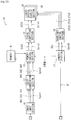
- FIG. 1 illustrates one configuration example of a display according to an embodiment of the present disclosure.
- a display 1 is a display that operates by a so-called field sequential driving scheme. It is to be noted that since a display control method and a display control device according to embodiments of the present disclosure are embodied by the present embodiment, description thereof will be made together with description of the display 1.
- the display 1 includes an image input section 11, a color correction section 12, a memory 9, a memory control section 13, a signal correction section 14, a liquid crystal display section 20, an analysis section 15, a threshold value setting section 16, a control section 17, a backlight control section 18, and a backlight 30.
- the image input section 11 is an interface used to input an image signal which may be an RGB signal from external equipment such as a PC (Personal Computer) and so forth.
- the image input section 11 is adapted to output the image signal so input as image signals SR1, SG1, and SB1, and a synchronous signal Sync1 that synchronizes with the image signals SR1, SG1, and SB1.
- the image signal SR1 is a signal that includes luminance information IR of red (R)
- the image signal SG1 is a signal that includes luminance information IG of green (G)
- the image signal SB1 is a signal that includes luminance information IB of blue (B).
- the color correction section 12 is adapted to perform color-related correction such as gamma correction, color irregularity correction and so forth on the basis of the image signals SR1, SG1, and SB1, and the synchronous signal Sync1.
- the color correction section 12 is configured to generate image signals SR2, SG2, and SB2 by performing such correction as mentioned above, and to generate a synchronous signal Sync2 that synchronizes with the image signals SR2, SG2, and SB2. It is to be noted that although in this example, the color correction section 12 is configured to perform the color-related correction, the color correction section 12 may be configured to perform signal processing other than the color-related correction.
- the memory 9 is a so-called frame memory that stores the luminance information IR included in the image signal SR2, the luminance information IG included in the image signal SG2, and the luminance information IB included in the image signal SB2 each by the amount of one frame.
- the memory 9 is configured such that operations of writing and reading-out the pieces of luminance information IR, IG, and IB into and from the memory 9 are controlled by the memory control section 13.
- the memory control section 13 is adapted to control the operations of writing and reading-out the pieces of luminance information IR, IG, and IB into and from the memory 9. Specifically, in the writing operation, the memory control section 13 makes the memory 9 store the pieces of luminance information IR, IG, and IB included in the image signals SR2, SG2, and SB2 on the basis of the image signals SR2, SG2, and SB2, and the synchronous signal Sync2. Thus, for example, the pieces of luminance information IR, IG, and IB corresponding to one frame may be stored into the memory 9.
- the memory control section 13 reads out only the luminance information to be displayed out of the pieces of one-frame luminance information IR, IG, and IB from the memory 9 in instructed order on the basis of a memory control signal SMEM as described later. Specifically, the memory control section 13 sequentially reads out any of the one-frame luminance information IR (a red image PR), the one-frame luminance information IG (a green image PG), and the one-frame luminance information IB (a blue image PB) in each subfield SF (described later) on the basis of the memory control signal SMEM.
- the one-frame luminance information IR a red image PR
- the one-frame luminance information IG a green image PG
- IB a blue image PB
- the memory control section 13 reads out only an image to be displayed out of the red image PR, the green image PG, and the blue image PB.
- the memory control section 13 is configured to then output one or more of the pieces of luminance information IR, IG, and IB read out from the memory 9 as an image signal SIG3 (a field sequential signal), and to generate and output a synchronous signal Sync3 that synchronizes with the image signal SIG3.
- the signal correction section 14 is adapted to perform signal correction on the basis of the image signal SIG3 and the synchronous signal Sync3. Specifically, the signal correction section 14 may be adapted to correct the one or more pieces of luminance information IR, IG, and IB on the basis of, for example, the one or more pieces of luminance information IR, IG, and IB in the plurality of adjacent subfields SF (described later). One example of such correction may include overdrive correction.
- the signal correction section 14 is configured to generate an image signal SIG4 by performing the above-mentioned correction, and to generate a synchronous signal Sync4 that synchronizes with the image signal SIG4.
- the liquid crystal display section 20 is adapted to perform display by driving liquid crystal display elements and modulating light emitted from the backlight 30.
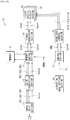
- Fig. 2 illustrates one example of a block diagram of the liquid crystal display section 20.
- the liquid crystal display section 20 includes a timing control section 21, a gate driver 22, a data driver 23, and a pixel array section 24.
- the timing control section 21 is adapted to control drive timings of the gate driver 22 and the data driver 23 on the basis of the image signal SIG4 and the synchronous signal Sync4, to generate an image signal Sdisp on the basis of the image signal SIG4, and to supply the image signal Sdisp to the data driver 23.
- the gate driver 22 is adapted to sequentially select and sequentially scan pixels Pix in the pixel array section 24 row by row in accordance with timing control by the timing control section 21.
- the data driver 23 is adapted to generate a pixel voltage Vpix which is an analog signal by performing D/A (digital/analog) conversion on the basis of the image signal Sdisp and to supply the pixel voltage Vpix to each pixel Pix in the pixel array section 24.
- the pixel array section 24 is a section in which the pixels Pix are arranged in a matrix.
- Each pixel Pix is adapted to perform display in time division on the basis of the pixel voltage Vpix corresponding to the luminance information IR, the pixel voltage Vpix corresponding to the luminance information IG, and the pixel voltage Vpix corresponding to the luminance information IB. That is, each pixel Pix does not include so-called sub-pixels and is configured to perform display of red, green, and blue in time division.
- the backlight 30 emits red light, green light, and blue light in time division in synchronization with a displaying operation on the pixel array section 24 as described later.
- the display 1 displays the red image PR, the green image PG, and the blue image PB in time division.
- the analysis section 15 is adapted to determine the image to be displayed out of the red image PR, the green image PG, and the blue image PB on the basis of the image signals SR2, SG2, and SB2 and the synchronous signal Sync1 and to output a result of determination as color information CI.
- the analysis section 15 may obtain a histogram concerning to luminance levels of, for example, the image signal SR2 on the basis of the one-frame luminance information IR included in the image signal SR2, and may determine that the red image PR is to be displayed when the luminance levels are equal to or are distributed above a predetermined luminance level (a threshold value Lth).
- the analysis section 15 determines that the red image is not to be displayed when all of the luminance levels of the one-frame luminance information IR are less than the threshold value Lth.
- the analysis section 15 determines whether the green image PG is to be displayed on the basis of the one-frame luminance information IG included in the image signal SG2 and determines whether the blue image PB is to be displayed on the basis of the one-frame luminance information IB included in the image signal SB2 in the same way. Then, the analysis section 15 is configured to output each result of determination so performed as the color information CI.
- the analysis section 15 performs determination using the histogram
- the way of determining the image to be displayed is not limited to the above-mentioned one, and, for example, the histogram may not be used.
- the luminance levels of the one-frame luminance information IR included in the image signal SR2 may be monitored, and when there exists a luminance level which is more than or equal to the predetermined luminance level (the threshold value Lth) in the luminance information IR, it may be determined that the red image PR is to be displayed.
- the threshold value Lth the predetermined luminance level
- the threshold value setting section 16 is adapted to supply the threshold value Lth to the analysis section 15.
- the threshold value Lth serves as an evaluation standard when the analysis section 15 determines the image to be displayed out of the red image PR, the green image PG, and the blue image PB. For example, 0 (zero) or a sufficiently low value which is higher than zero may be set as the threshold value Lth. In this case, it may be desirable to set the threshold value Lth in consideration of, for example, characteristics of gamma correction and so forth performed by the color correction section 12.
- the threshold value Lth may be set (preset) to a predetermined value in advance or a user may optionally set the threshold value Lth.
- the control section 17 is adapted to set the subfields SF of the number which is the same as the number of the images to be displayed out of the red image PR, the green image PG, and the blue image PB in a one-frame period on the basis of the color information CI, and to control the display 1 so as to display the images in the respective subfields SF.
- the control section 17 may set three subfields SF in the one-frame period. Then, the control section 17 controls the display 1 so as to display the red image PR, the green image PG, and the blue image PB in this order in the three subfields SF. It is to be noted that although in this example, the images are displayed in order of the red image PR, the green image PG, and the blue image PB, the order is not limited to the above-mentioned one and the images may be displayed in any other order.
- the control section 17 may set two subfields SF in the one-frame period. Then, the control section 17 may control the display 1 so as to sequentially display these two images in the two subfields SF.
- the control section 17 may set one subfield SF in the one-frame period. Then, the control section 17 may control the display 1 so as to display this one image in the one subfield SF.
- the control section 17 generates the memory control signal SMEM and a backlight control signal SBL when performing the above-mentioned processing.
- the memory control signal SMEM is a signal used to control the operation of reading out the pieces of luminance information IR, IG, and IB from the memory 9 in accordance with the subfield(s) SF so set. Specifically, when the red image PR is to be displayed in a certain subfield SF, the control section 17 instructs the memory control section 13 using the memory control signal SMEM so as to read out the one-frame luminance information IR from the memory 9 and to output the read-out luminance information IR as the image signal SIG3.
- the control section 17 instructs the memory control section 13 using the memory control signal SMEM so as to read out the one-frame luminance information IG from the memory 9 and to output the read-out luminance information IG as the image signal SIG3 in the same way.
- the control section 17 instructs the memory control section 13 using the memory control signal SMEM so as to read out the one-frame luminance information IB from the memory 9 and to output the read-out luminance information IB as the image signal SIG3 in the same way.
- the backlight control signal SBL is a signal used to control a light emitting operation of the backlight 30 in accordance with the set subfield(s) SF. Specifically, when the red image PR is to be displayed in the certain subfield SF, the control section 17 instructs the backlight control section 18 so as to make a light emitting section 30R (described later) of the backlight 30 emit light using the backlight control signal SBL.
- the control section 17 instructs the backlight control section 18 so as to make a light emitting section 30G (described later) of the backlight 30 emit light using the backlight control signal SBL, and when the blue image PB is to be displayed in the certain subfield SF, the control section 17 instructs the backlight control section 18 so as to make a light emitting section 30B (described later) of the backlight 30 emit light using the backlight control signal SBL in the same way.
- the control section 17 also has a function of generating and outputting a synchronous signal SyncB that synchronizes with the backlight control signal SBL.
- the backlight control section 18 is adapted to generate light emission control signals CTLR, CTLG, and CTLB on the basis of the backlight control signal SBL and the synchronous signal SyncB.
- the light emission control signal CTLR is a signal used to control light emission of the light emitting section 30R (described later) of the backlight 30
- the light emission control signal CTLG is a signal used to control light emission of the light emitting section 30G (described later)
- the light emission control signal CTLB is a signal used to control light emission of the light emitting section 30B (described later).
- the light emission control signals CTLR, CTLG, and CTLB are used to indicate light emission timings, light emission periods, light emission luminances to the respective light emitting sections 30R, 30G, and 30B.
- the backlight 30 is adapted to independently emit the red light, the green light, and the blue light on the basis of the light emission control signals CTLR, CTLG, and CTLB and radiate the light so emitted to the liquid crystal display section 20.
- Fig. 3 schematically illustrates one configuration example of the backlight 30.
- the backlight 30 includes the light emitting sections 30R, 30G, and 30B.
- Each of the light emitting sections 30R, 30G, and 30B may be configured by using, for example, an LED (Light Emitting Diode).
- the light emitting section 30R performs surface-emission of the red (R) light on the basis of the light emission control signal CTLR
- the light emitting section 30G performs surface-emission of the green (G) light on the basis of the light emission control signal CTLG
- the light emitting section 30B performs surface-emission of the blue (B) light on the basis of the light emission control signal CTLB.
- the light emitting sections 30R, 30G, and 30B may emit light independently from one another.
- the image(s) to be displayed out of the red image PR, the green image PG, and the blue image PB is/are determined so as to dynamically change the number of subfields SF in the one-frame period in this way.
- the display 1 is configured to make it possible to increase display luminance and to make it possible to reduce power consumption when such an image that only one or two of the red light, the green light, and the blue light is/are used is to be displayed as in the case of a so-called blue screen as described later.
- the light emitting sections 30R, 30G, and 30B correspond to one specific example of a "plurality of light emitting sections" in one embodiment of the present disclosure.
- the analysis section 15, the control section 17, and the backlight control section 18 correspond to one specific example of a "light emission control section” in one embodiment of the present disclosure.
- the liquid crystal display section 20 corresponds to one specific example of a "display section” in one embodiment of the present disclosure.
- Each of the pieces of the luminance information IR, IG, and IB corresponds to one specific example of "luminance information" in one embodiment of the present disclosure.
- the memory control section 13 corresponds to one specific example of a "display control section” in one embodiment of the present disclosure.
- the image input section 11 inputs an image signal from external equipment.
- the color correction section 12 performs the color-related correction such as the gamma correction, the color irregularity correction and so forth on the image signal and generates the image signals SR2, SG2, and SB2.
- the analysis section 15 determines the image to be displayed out of the red image PR, the green image PG, and the blue image PB on the basis of the image signals SR2, SG2, and SB2 and outputs the result of determination as the color information CI.
- the control section 17 sets the subfields SF of the number which is the same as the number of the images to be displayed out of the red image PR, the green image PG, and the blue image PB in the one-frame period on the basis of the color information CI, and generates the memory control signal SMEM and the backlight control signal SBL.
- the memory 9 stores the pieces of luminance information IR, IG, and IB included in the image signals SR2, SG2, and SB2.
- the memory control section 13 controls the operations of writing and reading out the pieces of luminance information IR, IG, and IB into and from the memory 9 on the basis of the memory control signal SMEM and outputs the read-out pieces of luminance information IR, IG, and/or IB as the image signal SIG3.
- the signal correction section 14 performs signal correction on the image signal SIG3.
- the liquid crystal display section 20 performs display by driving the liquid crystal display elements and modulating the light radiated from the backlight 30.
- the backlight control section 18 generates the light emission control signals CTLR, CTLG, and CTLB on the basis of the backlight control signal SBL.
- the light emitting section 30R of the backlight 30 performs surface-emission of the red light on the basis of the light emission control signal CTLR
- the light emitting section 30G performs surface-emission of the green light on the basis of the light emission control signal CTLG
- the light emitting section 30B performs surface-emission of the blue light on the basis of the light emission control signal CTLB.
- the display 1 will be described.
- description will be made by giving the following three cases C1 to C3 as examples.
- the case C1 a case where a usual and general image is to be displayed is assumed.
- the case C1 is applied when the pieces of luminance information IR, IG, and IB having luminance levels that are more than or equal to the threshold value Lth are included in the respective pieces of one-frame luminance information IR, IG, and IB.
- the case C2 a case where an image in which a black letter or character is arranged against the yellow background is to be displayed is assumed.
- the case C2 is applied when although the pieces of luminance information IR and IG having the luminance levels that are more than or equal to the threshold value Lth are included in the respective pieces of one-frame luminance information IR and IG, the luminance information IB having the luminance levels that are more than or equal to the threshold value Lth is not included in the one-frame luminance information IB.
- the case C3 a case where, for example, an image (the so-called blue screen) in which the black letter or character is arranged against the blue background is to be displayed is assumed.
- the case C3 is applied when although the luminance information IB having the luminance levels that are more than or equal to the threshold value Lth is included in the one-frame luminance information IB, the pieces of luminance information IR and IG having the luminance levels that are more than or equal to the threshold value Lth are not included in the respective pieces of one-frame luminance information IR and IG.
- the analysis section 15 determines that all of the red image PR, the green image PG, and the blue image PB are to be displayed and informs the control section 17 of that determination using the color information CI.
- the control section 17 sets three subfields SF in the one-frame period and generates the memory control signal SMEM and the backlight control signal SBL.
- the memory control section 13 reads out the one-frame luminance information IR (the red image PR), the one-frame luminance information IG (the green image PG), and the one-frame luminance information IB (the blue image PB) in these respective three subfields SF from the memory 9 on the basis of the memory control signal SMEM, and outputs the information so read-out as the image signal SIG3. Then, the signal correction section 14 performs correction on the image signal SIG3 and generates the image signal SIG4. In addition, the backlight control section 18 generates the light emission control signals CTLR, CTLG, and CTLB on the basis of the backlight control signal SBL.
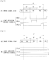
- Fig. 4 illustrates one example of the operation of the display 1 in the case C1, in which (A) schematically illustrates an example of the image signal SIG4 and (B) illustrates examples of waveforms of the light emission control signals CTLR, CTLG, and CTLB.
- "PR" indicates the one-frame luminance information IR (the red image PR)
- "PG” indicates the one-frame luminance information IG (the green image PG)
- "PB” indicates the one-frame luminance information IB (the blue image PB).
- a high level indicates light emission and a low level indicates light extinction in each of the light emission control signals CTLR, CTLG, and CTLB.
- the one-frame luminance information IR (the red image PR) is supplied to the liquid crystal display section 20 ((A) of Fig. 4 ), and the high-level light emission control signal CTLR and the low-level light emission control signals CTLG and CTLB are supplied to the backlight 30 ((B) of Fig. 4 ) in the first subfield SF in the one-frame period.
- the liquid crystal display section 20 displays the red image PR and the light emitting section 30R of the backlight 30 emits the red light.
- the one-frame luminance information IG (the green image PG) is supplied to the liquid crystal display section 20 ((A) of Fig.
- the liquid crystal display section 20 displays the green image PG and the light emitting section 30G of the backlight 30 emits the green light.
- the one-frame luminance information IB (the blue image PB) is supplied to the liquid crystal display section 20 ((A) of Fig. 4 ), and the high-level light emission control signal CTLB and the low-level light emission control signals CTLR and CTLG are supplied to the backlight 30 ((B) of Fig. 4 ) in the third subfield SF.
- the liquid crystal display section 20 displays the blue image PB and the light emitting section 30B of the backlight 30 emits the blue light.
- the display 1 displays a colored image by displaying the red image PR, the green image PG, and the blue image PB in time division in this way.
- the analysis section 15 determines that only the red image PR and the green image PG are to be displayed and informs the control section 17 of this determination using the color information CI.
- the control section 17 sets two subfields SF in the one-frame period and generates the memory control signal SMEM and the backlight control signal SBL.
- the memory control section 13 reads out the one-frame luminance information IR (the red image PR) and the one-frame luminance information IG (the green image PG) from the memory 9 in the respective two subfields SF on the basis of the memory control signal SMEM, and outputs the information so read-out as the image signal SIG3. That is, the memory control section 13 does not read out the one-frame luminance information IB (the blue image PB) from the memory 9. Then, the signal correction section 14 performs correction on the image signal SIG3 and generates the image signal SIG4. In addition, the backlight control section 18 generates the light emission control signals CTLR, CTLG, and CTLB on the basis of the backlight control signal SBL.
- Fig. 5 illustrates one example of the operation of the display 1 in the case C2, in which (A) schematically illustrates one example of the image signal SIG4 and (B) illustrates examples of the waveforms of the light emission control signals CTLR, CTLG, and CTLB.
- the one-frame luminance information IR (the red image PR) is supplied to the liquid crystal display section 20 ((A) of Fig. 5 ) and the high-level light emission control signal CTLR and the low-level light emission control signals CTLG and CTLB are supplied to the backlight 30 ((B) of Fig. 5 ) in the first subfield SF in the one-frame period.
- the liquid crystal display section 20 displays the red image PR and the light emitting section 30R of the backlight 30 emits the red light.
- the one-frame luminance information IG (the green image PG) is supplied to the liquid crystal display section 20 ((A) of Fig. 5 ) and the high-level light emission control signal CTLG and the low-level light emission control signals CTLR and CTLB are supplied to the backlight 30 ((B) of Fig. 5 ) in the second subfield SF.
- the liquid crystal display section 20 displays the green image PG and the light emitting section 30G of the backlight 30 emits the green light.
- the display 1 displays a yellow image by displaying the red image PR and the green image PG, in time division in this way.
- the analysis section 15 determines that display of the blue image PB is not necessary and the display 1 displays the two images (the red image PR and the green image PG) excluding the blue image PB in time division.
- the analysis section 15 determines that only the blue image PB is to be displayed and informs the control section 17 of this determination using the color information CI.
- the control section 17 sets one subfield SF in the one-frame period and generates the memory control signal SMEM and the backlight control signal SBL.
- the memory control section 13 reads out the one-frame luminance information IB (the blue image PB) from the memory 9 in the one subfield SF and outputs the information so read-out as the image signal SIG3. That is, the memory control section 13 does not read out the one-frame luminance information IR (the red image PR) and the one-frame luminance information IG (the green image PG) from the memory 9. Then, the signal correction section 14 performs correction on the image signal SIG3 and generates the image signal SIG4. In addition, the backlight control section 18 generates the light emission control signals CTLR, CTLG, and CTLB on the basis of the backlight control signal SBL.
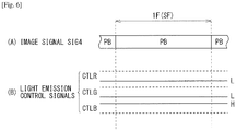
- Fig. 6 illustrates one example of the operation of the display 1 in the case C3, in which (A) schematically illustrates one example of the image signal SIG4 and (B) illustrates examples of the waveforms of the light emission control signals CTLR, CTLG, and CTLB.
- the one-frame luminance information IB (the blue image PB) is supplied to the liquid crystal display section 20 ((A) of Fig. 6 ) and the high-level light emission control signal CTLB and the low-level light emission control signals CTLR and CTLG are supplied to the backlight 30 ((B) of Fig. 6 ) in the one-frame period (the subfield SF).
- the liquid crystal display section 20 displays the blue image PB and the light emitting section 30B of the backlight 30 emits the blue light.
- the display 1 displays only the blue image PB in this way. That is, since all of the luminance levels of each of the pieces of one-frame luminance information IR and IG are less than the threshold value Lth, the analysis section 15 determines that display of the red image PR and the green image PG is not necessary and the display 1 displays only the blue image PB.
- the analysis section 15 determines the image(s) to be displayed out of the red image PR, the green image PG, and the blue image PB in this way. Then, the control section 17 dynamically changes the number of the subfields SF in the one-frame period in accordance with the number of images to be displayed out of the red image PR, the green image PG, and the blue image PB on the basis of a result of the above-mentioned determination, and controls the display 1 so as to display the images in the respective subfields SF.
- the display 1 whether the image that has been supplied is the usual image (for example, the case C1) or the image that only one or two of the red light, the green light, and the blue light is/are used as in the case of the so-called blue screen (for example, the case C2 or C3) is determined, and in the latter case, the number of the subfields SF in the one-frame period is reduced.
- the display luminance of the display 1 it is possible to increase the display luminance of the display 1 and it is also possible to reduce the power consumption when the image that only one or two of the red light, the green light, and the blue light is/are used is to be displayed as described below in comparison with a comparative example.
- the display 1R is adapted to constantly set three subfields SF in the one-frame period.
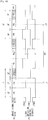
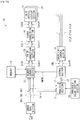
- Fig. 7 illustrates one configuration example of the display 1R according to the comparative example.
- the display 1R includes a control section 13R.
- the control section 13R is adapted to control the operations of writing and reading out the pieces of luminance information IR, IG, and/or IB into and from the memory 9 on the basis of the image signals SR2, SG2, and SB2, and the synchronous signal Sync2, and to output the read-out pieces of luminance information IR, IG, and/or IB as the image signal SIG3.
- control section 13R constantly sets the three subfields SF in the one-frame period, reads out the one-frame luminance information IR (the red image PR), the one-frame luminance information IG (the green image PG), and the one-frame luminance information IB (the blue image PB) in the respective three subfields SF, and outputs the read-out information as the image signal SIG3.
- control section 13R also has a function of generating the light emission control signals CTLR, CTLG, and CTLB that synchronize with display of the red image PR, the green image PG, and the blue image PB.
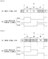
- Fig. 8 illustrates one example of the operation of the display 1R in the case C2
- Fig. 9 illustrates one example of the operation of the display 1R in the case C3.
- (A) schematically illustrates one example of the image signal SIG4
- (B) illustrates examples of the waveforms of the light emission control signals CTLR, CTLG, and CTLB.
- CTLR light emission control signals
- CTLG light emission control signals
- CTLB the operation of the display 1R in the case C1 is the same as that in the case ( Fig. 4 ) of the present embodiment.
- the control section 13R sets the three subfields SF in the one-frame period irrespective of the cases C1 to C3 in this way.
- the liquid crystal display section 20 displays the red image PR and the light emitting section 30R of the backlight 30 emits the red light in the first subfield SF in the one-frame period
- the liquid crystal display section 20 displays the green image PG and the light emitting section 30G of the backlight 30 emits the green light in the second subfield SF
- the liquid crystal display section 20 displays the blue image PB and the light emitting section 30B of the backlight 30 emits the blue light in the third subfield SF.
- the blue image PB is displayed as a near black blue image. Therefore, in the example in Fig. 8 , although the light emitting section 30B emits light, the display 1R performs black display and therefore a period that hardly contributes to display is created in the third subfield SF. In the case C3, since all of the luminance levels of each of the pieces of one-frame luminance information IR and IG are less than the threshold value Lth, both of the red image PR and the green image PG are displayed as near black images similarly. Therefore, in the example in Fig. 9 , although the light emitting sections 30R and 30G emit light, the display 1R performs the black display and therefore the period that hardly contributes to display is created in each of the first and second subfields SF.
- the display 1R according to the comparative example Since in the display 1R according to the comparative example, the number of subfields SF in the one-frame period has been fixed to three as described above, the period that hardly contributes to display is created when the image in which only one or two of the red light, the green light, and the blue light is/are used is to be displayed as in the case of the so-called blue screen. In such a period, the power consumption may possibly be wasted due to light emission of the backlight 30 (the light emitting sections 30R, 30G, and 30B).
- the display 1 is configured such that the image(s) to be displayed out of the red image PR, the green image PG, and the blue image PB is/are determined and the number of subfields SF in the one-frame period is dynamically changed depending on the image(s) to be displayed.
- the display luminance of the display 1 since it is possible to omit the period that does not contribute to display in the display 1, it is possible to increase the display luminance of the display 1 and it is also possible to suppress waste of the power consumption. That is, for example, as to the case C2, the example in Fig.
- the embodiment may correspond to an example in which the light emission period (the third subfield SF) of the light emitting section 30B is omitted and the light emission periods (the first and second subfields SF) of the light emitting sections 30R and 30G are lengthened in Fig. 8 according to the comparative example.
- the light emission period (the third subfield SF) of the light emitting section 30B is omitted and the light emission periods (the first and second subfields SF) of the light emitting sections 30R and 30G are lengthened in Fig. 8 according to the comparative example.
- the 6 according to the present embodiment may correspond to an example in which the light emission periods (the first and second subfields SF) of the light emitting sections 30R and 30G are omitted and the light emission period (the third subfield SF) of the light emitting section 30B is lengthened in Fig. 9 according to the comparative example in the same way.
- the light emission periods (the first and second subfields SF) of the light emitting sections 30R and 30G are omitted and the light emission period (the third subfield SF) of the light emitting section 30B is lengthened in Fig. 9 according to the comparative example in the same way.
- the liquid crystal display section 20 since in the display 1R according to the comparative example, the three subfields are constantly set in the one-frame period, it is necessary for the liquid crystal display section 20 to perform scan driving three times in the one-frame period constantly and therefore the power consumption may possibly be increased.
- the number of subfields SF in the one-frame period is dynamically changed, it is possible to reduce the number of times of performing scan driving by the liquid crystal display section 20 depending on the image(s) to be displayed and therefore it is possible to reduce the power consumption.
- the number of subfields SF in the one-frame period is dynamically changed as described above, it is possible to increase the display luminance and the image quality of the display and it is also possible to reduce the power consumption when such display that only one or two of the red light, the green light, and the blue light is/are used is to be performed as in the case of the blue screen.
- the backlight control section 18 may be configured to set a start timing and a finish timing of each pulse (a pulse phase and a pulse width) in each of the light emission control signals CTLR, CTLG, and CTLB, for example, as illustrated in Fig. 10 .
- the timings are set such that the pulse widths of the light emission control signals CTLR, CTLG, and CTLB are made different from one another.
- each of the light emitting sections 30R, 30G, and 30B emit light at a timing that liquid crystal response and so forth of the liquid crystal display section 20 are taken into account, by configuring so as to set the start timing and the finish timing of each pulse as described above.
- one subfield SF has been set in the one-frame period when one of the red image PR, the green image PG, and the blue image PB is to be displayed (for example, the case C3)
- the present disclosure is not limited to this configuration.
- a plurality (in this example, three) of the subfields SF may be set in the one-frame period and the same image (in this example, the blue image PB) may be repetitively displayed.
- scan driving is performed a plurality of times (in this example, three times) in the one-frame period in the liquid crystal display section 20, it is possible to reduce degradation of image quality caused by leakage in a transistor of the pixel Pix.
- a configuration that allows setting of the start timing and the finish timing (the pulse phase and the pulse width) of each pulse in each of the light emission control signals CTLR, CTLG, and CTLB may be possible as illustrated in Fig. 12 .
- the two subfields have been set in the one-frame period when two of the red image PR, the green image PG, and the blue image PB are to be displayed (for example, the case C2)
- the present disclosure is not limited to this configuration.
- three or more subfields SF may be set in the one-frame period or one subfield SF may be set in the one-frame period.
- the present modification example will be described in detail by giving several examples thereof.
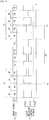
- the display 2 is adapted to set four subfields SF in the one-frame period in the case C2.
- Fig. 13 illustrates one example of the operation of the display 2 in the case C2, in which (A) schematically illustrates one example of the image signal SIG4 and (B) illustrates examples of the waveforms of the light emission control signals CTLR, CTLG, and CTLB.
- the display 2 sets the four subfields SF in the one-frame period in the case C2.
- the one-frame luminance information IR (the red image PR) is supplied to the liquid crystal display section 20 ((A) of Fig. 13 ) and the high-level light emission control signal CTLR and the low-level light emission control signals CTLG and CTLB are supplied to the backlight 30 ((B) of Fig. 13 ) in the first subfield SF.
- the liquid crystal display section 20 displays the red image PR and the light emitting section 30R of the backlight 30 emits the red light.
- the one-frame luminance information IG (the green image PG) is supplied to the liquid crystal display section 20 ((A) of Fig. 13 ) and the high-level light emission control signal CTLG and the low-level light emission control signals CTLR and CTLB are supplied to the backlight 30 ((B) of Fig. 13 ) in the second subfield SF.
- the liquid crystal display section 20 displays the green image PG and the light emitting section 30G of the backlight 30 emits the green light.
- the one-frame luminance information IR (the red image PR) which is the same as the information in the first subfield SF is again supplied to the liquid crystal display section 20 ((A) of Fig. 13 ) and the high-level light emission control signal CTLR and the low-level light emission control signals CTLG and CTLB are supplied to the backlight 30 ((B) of Fig. 13 ) in the third subfield SF.
- the liquid crystal display section 20 displays the red image PR and the light emitting section 30R of the backlight 30 emits the red light.
- the one-frame luminance information IG (the green image PG) which is the same as the information in the second subfield SF is again supplied to the liquid crystal display section 20 ((A) of Fig.
- the liquid crystal display section 20 displays the green image PG and the light emitting section 30G of the backlight 30 emits the green light.
- the display 2 displays the red image PR and the green image PG two times per image in time division in the one-frame period in this way. For example, it is possible to reduce the probability that a viewer feels as if the image quality has been reduced when the viewer has not viewed a display screen for a very short period of time by blinking eyes as described below in comparison with the display 1R according to the comparative example.
- Fig. 14 illustrates one example of the operation of the display 1R according to the comparative example in the case C2
- Fig. 15 illustrates one example of the operation of the display 2 according to the modification example in the case C2.
- (A) schematically illustrates one example of the image signal SIG4
- (B) illustrates examples of the waveforms of the light emission control signals CTLR, CTLG, and CTLB.
- the viewer when the viewer has not observed the display screen of the display 1R in a very short period PV from timings t1 to t2, the viewer may possibly see a color which is different from the original color immediately before the timing t1 and immediately after the timing t2 as illustrated in Fig. 14 . Specifically, in this example, the viewer may possibly recognize that a somewhat reddish image is displayed on the display screen immediately before the timing t1 and may possibly recognize that a somewhat greenish image is displayed on the display screen immediately after the timing t2. In the display 1R according to the comparative example, the viewer may possibly feel that the image quality has been reduced due to occurrence of so-called "color breakup" as described above.
- the display 2 according to the present modification example it is possible for the viewer to see the color which is almost the same as the original color even immediately before the timing t1 and immediately after the timing t2 as illustrated in Fig. 15 . That is, since in the display 2, many subfields SF are set in the one-frame period, it is possible to reduce the possibility of occurrence of the color breakup and therefore it is possible to increase the image quality.
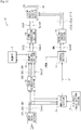
- the display 3 is adapted to set one subfield SF in the one-frame period and to make two of the light emitting sections 30R, 30G, and 30B emit light.
- Fig. 16 illustrates one configuration example of the display 3 according to the present modification example.
- the display 3 includes a control section 47 and a signal generation section 43.
- the control section 47 is adapted to set one or the plurality of subfields SF in the one-frame period on the basis of the color information CI and to control the display 3 so as to display each image in each of the subfields SF as in the control section 17 according to the above-mentioned embodiment.
- the control section 47 sets one subfield SF in the one-frame period.
- the control section 47 generates a control signal SSIG indicating that the two images correspond to which images of the red image PR, the green image PG, and the blue image PB.
- control section 47 operates in the same way as the control section 17.
- the signal generation section 43 is adapted to generate an image signal S10 and a synchronous signal Sync10 that synchronizes with the image signal S10 on the basis of the image signals SR2, SG2, and SB2, the synchronous signal Sync2, and the control signal SSIG.
- the signal generation section 43 when two of the red image PR, the green image PG, and the blue image PB are to be displayed (for example, the case C2), the signal generation section 43 generates an image of a combination color of those two images on the basis of the control signal SSIG and outputs the image so generated as the image signal S10. Specifically, for example, when the control signal SSIG indicates that the red image PR and the green image PG are to be displayed, the signal generation section 43 may generate a yellow image PY and may output the image signal S10 that includes luminance information IY of yellow (Y).
- the signal generation section 43 may generate a cyan image PC and may output the image signal S10 that includes luminance information IC of cyan (C).
- the signal generation section 43 may generate a magenta image PM and may output the image signal S10 that includes luminance information IM of magenta (M).
- RGB/YUV conversion may be performed on the basis of the pieces of luminance information IR, IG, and IB included in the image signals SR2, SG2, and SB2 and a Y component in the YUV signal so converted may be used as the pieces of luminance information IY, IC, and IM.
- the signal generation section 43 may not generate any image and may output the image signals SR2, SG2, and SB2 as the image signal S10 as they are.
- the control section 47 may set one subfield SF in the one-frame period and may generate the control signal SSIG owing to the above-mentioned configuration.
- the signal generation section 43 may generate an image of a combination color of these two images and may output the image as the image signal S10 on the basis of the control signal SSIG.
- the signal generation section 43 corresponds to one specific example of a "luminance information generation section" in one embodiment of the present disclosure.
- Fig. 17 illustrates one example of the operation of the display 3 in the case C2, in which (A) schematically illustrates one example of the image signal SIG4 and (B) illustrates examples of the waveforms of the light emission control signals CTLR, CTLG, and CTLB.
- the analysis section 15 determines that two images, i.e., the red image PR and the green image PG are to be displayed, the signal generation section 43 generates the yellow image PY.
- luminance information that configures the yellow image PY is supplied to the liquid crystal display section 20 ((A) of Fig. 17 ) and the high-level light emission signals CTLR and CTLG and the low-level light emission control signal CTLB are supplied to the backlight 30 ((B) of Fig. 17 ) in the one-frame period (the subfield SF).
- the liquid crystal display section displays the yellow image PY and the backlight 30 emits yellow light as red and green combination light.
- the light emission control signals CTLR, CTLG, and CTLB have been made to be maintained at the high levels or the low levels over the period of the subfield SF
- the present disclosure is not limited to this configuration.
- the start timing and the finish timing (the pulse phase and the pulse width) of each pulse in each of the light emission control signals CTLR, CTLG, and CTLB may be changed, for example, as illustrated in Fig. 18 .
- this combination ratio may be changed, for example, using the pieces of luminance information IR, IG, and IB.
- the backlight 30 it is possible for the backlight 30 to emit light in a color according to the pieces of luminance information IR, IG, and IB.
- one or more of the light emission control signals CTLR, CTLG, and CTLB may be configured by a plurality of pulses as illustrated in Fig. 19 . In this case, it is possible to reduce the probability that color breakup occurs and therefore it is possible to increase the image quality as in the case of the display 2 according to the above-mentioned present modification example.
- a color of the light that the backlight 30 emits may be adjusted by changing the emission luminances of the respective light emitting sections 30R, 30G, and 30B by changing the signal levels of the light emission control signals CTLR, CTLG, and CTLB, for example, as illustrated in Fig. 20 .
- the emission luminance of the light emitting section 30G is made lower than the emission luminance of the light emitting section 30R by supplying a voltage VH to the light emitting section 30R and supplying a voltage VM which is lower than the voltage VH to the light emitting section 30G.
- the emission luminances of the light emitting sections 30R, 30G, and 30B have been adjusted by supplying voltages, the present disclosure is not limited to this. Alternatively, the emission luminances may be adjusted, for example, by supplying currents to the light emitting sections.
- one subfield SF has been set in the one-frame period and two of the light emitting sections 30R, 30G, and 30B have been made to emit light in the case C2, the present disclosure is not limited to this.
- one subfield SF may be set in the one-frame period and all of the light emitting sections 30R, 30G, and 30B may be made to emit light in the case C1.
- the analysis section 15 has determined the image(s) to be displayed out of the red image PR, the green image PG, and the blue image PB on the basis of the image signals SR2, SG2, and SB2 and the synchronous signal Sync2 which are the output signals from the color correction section 12, the present disclosure is not limited to this configuration.
- the analysis section 15 may perform this processing (image determination) on the basis of the image signals SR1, SG1, and SB1 and the synchronous signal Sync1 which are the input signals into the color correction section 12.
- the display 1 includes the analysis section 15, the present disclosure is not limited to this configuration.
- the analysis section 15 may not be included when it is possible to supply the color signal (the color information) CI from the outside, for example, as in a display 1B illustrated in Fig. 22 .
- a circuit that is disposed at a stage preceding the display 1B performs analysis of the image to be displayed in the display 1B and outputs the color signal CI
- application of the present modification example is possible.
- the image signals and the color signal CI have been made to be separately supplied, the present disclosure is not limited to this configuration and they may be supplied, for example, in the form of one time-division-multiplexed signal.
- an operation mode setting section 49 that sets one of a plurality of operation modes including a normal display mode M1 and a monochromatic display mode M2 may be included so as to make the operation mode setting section 49 generate the color information CI.
- the operation mode setting section 49 may generate the color information CI indicating that all of the red image PR, the green image PG, and the blue image PB are to be displayed and the display 1C may operate in a manner as in the case C1.
- the operation mode setting section 49 may generate the color information CI indicating, for example, that only the blue image PB is to be displayed and the display 1C may operate in a manner as in the case C3.
- the display 1C may operate in a manner as in the case C3.
- the color correction section 12 has been provided at the upstream of the memory control section 13, the present disclosure is not limited to this configuration.
- a color correction section 12D may be provided at the downstream of the memory control section 13, for example, as in a display 1D illustrated in Fig. 24 .
- the color correction section 12D performs color-related correction on the basis of the image signal SIG3 and the synchronous signal Sync3 output from the memory control section 13.
- the color correction section 12D generates an image signal SIG11 by performing the correction, generates a synchronous signal Sync11 that synchronizes with the image signal SIG11, and supplies the generated signals to the signal correction section 14.
- the signal correction section 14 has been provided at the downstream of the memory control section 13, the present disclosure is not limited to this configuration. Alternatively, the signal correction section 14 may be provided, for example, at the upstream of the memory control section 13. In the following, a display 1E according to the present modification example will be described.
- Fig. 25 illustrates one configuration example of the display 1E.
- the display 1E includes a control section 17E and a signal correction section 14E.
- the control section 17E has a function which is the same as that of the control section 17 according to the above-mentioned embodiment, and is configured to generate subfield information INFO indicating which one of the red image PR, the green image PG, and the blue image PB is made in one-to-one correspondence with which subfield SF and to supply the information INFO to the signal correction section 14E.
- the signal correction section 14E performs correction on the signal received on the basis of the image signals SR2, SG2, and SB2 and the synchronous signal Sync2 output from the color correction section 12.
- the signal correction section 14E performs correction based on the pieces of luminance information IR, IG, and IB in the plurality of adjacent subfields SF in the same way as the signal correction section 14. In that case, the signal correction section 14E performs this correction on the basis of the subfield information INFO. Then, the signal correction section 14E generates image signals SR12, SG12, and SB12 by performing the above-mentioned correction and a synchronous signal Sync12 that synchronizes with the image signals SR12, SG12, and SB12, and supplies the generated signals to the memory control section 13 and the analysis section 15.
- the RGB signal has been made to be input into the display 1
- the present disclosure is not limited to this configuration, and a signal of any other format may be input into the display.
- a display 1F into which a YUV signal is input will be described.
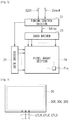
- Fig. 26 illustrates one configuration example of the display 1F.
- the display 1F includes an image input section 11F and a signal conversion section 40F.
- the image input section 11F is adapted to output image signals which are in the form of the YUV signal as image signals SY, SU, and SV, and a synchronous signal Sync0 that synchronizes with the image signals SY, SU, and SV.
- the signal conversion section 40F is adapted to convert (the YUV/RGB conversion) the YUV signal into an RGB signal.
- the signal conversion section 40F performs the YUV/RGB conversion on the basis of the image signals SY, SU, and SV that configure the YUV signal and the synchronous signal Sync0, and generates the image signals SR1, SG1, and SB1 that configure the RGB signal and the synchronous signal Sync1.
- the signal conversion section 40F corresponds to one specific example of a "conversion section" in one embodiment of the present disclosure. It is to be noted that although in this example, the signal conversion section 40F has been provided at the upstream of the color correction section 12, the present disclosure is not limited to this, and the signal conversion section 40F may be provided at any location as long as it is provided at the upstream of the memory control section 13.
- the memory control section 13 has been configured to write the pieces of one-frame luminance information IR, IG, and IB included in the image signals SR2, SG2, and SB2 into the memory 9 and to read out only the luminance information to be displayed among them from the memory 9, the present disclosure is not limited to this configuration.
- the memory control section 13 may be configured to write only the luminance information to be displayed into the memory 9.
- the emission luminances of the light emitting sections 30R, 30G, and 30B have been fixed regardless of the number of the subfields SF in the one-frame period, the present disclosure is not limited to this configuration.
- the emission luminances of the light emitting sections 30R, 30G, and 30B may be set to be reduced, for example, as the number of the subfields SF is reduced.
- the possibility that the viewer feels unnaturalness due to a rapid increase in display luminance is reduced.
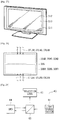
- Fig. 27 illustrates one example of the outside appearance of a television apparatus to which the display according to any of the above-mentioned embodiment and modification examples is applied.
- the television apparatus may include, for example, an image display screen section 510 including a front panel 511 and a filter glass 512, and the image display screen section 510 is configured by the display according to any of the above-mentioned embodiment and modification examples.
- the backlight 30 includes the three light emitting sections 30R, 30G, and 30B
- the present disclosure is not limited to this configuration.
- the backlight may include two or less, or four or more light emitting sections that emit light of different colors from one another, and/or may include a light emitting section or sections that emit(s) light of a color or colors other than red, green, and blue.
- the backlight 30 includes the light emitting sections 30R, 30G, and 30B
- the present disclosure is not limited to this configuration.
- the backlight may include light emitting sections 30AR, 30AG, and 30AB on its upper half part and light emitting sections 30BR, 30BG, and 30BB on its lower half part as in, for example, a backlight 30G illustrated in Fig. 28 .
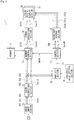
- the light emitting sections 30AR, 30AG, and 30AB are adapted to respectively emit the red (R) light, the green (G) light, and the blue (B) light on the basis of light emission control signals CTLAR, CTLAG, and CTLAB, and the light emitting sections 30BR, 30BG, and 30BB are adapted to respectively emit the red (R) light, the green (G) light, and the blue (B) light on the basis of light emission control signals CTLBR, CTLBG, and CTLBB in the same way.
- the present disclosure has been applied to the liquid crystal display, the present disclosure is not limited to this application. It is possible to apply the present disclosure to any display as long as it is the display of the type configured by a display device and a light emitting device other than a so-called self-emitting type display. Specifically, the present disclosure may be applied to a display, for example, using DLP (a registered trademark) (Digital Light Processing) technology.
- Fig. 29 schematically illustrates one example of a projector 60 using the DLP technology.
- the projector 60 includes a light source system 61, a prism 63, a DMD (Digital Mirror Device) 64, and a projection lens 65.
- the red (R) light, the green (G) light, and the blue (B) light are radiated in time division from the light source system 61.
- the light of each color is incident upon the DMD 64 that includes a plurality of movable micro-mirrors via the prism 63.
- the light reflected from the DMD 64 is incident upon the projection lens 65 again via the prism 63 and projected onto the screen.
Landscapes
- Engineering & Computer Science (AREA)
- Physics & Mathematics (AREA)
- Computer Hardware Design (AREA)
- General Physics & Mathematics (AREA)
- Theoretical Computer Science (AREA)
- Multimedia (AREA)
- Chemical & Material Sciences (AREA)
- Crystallography & Structural Chemistry (AREA)
- Control Of Indicators Other Than Cathode Ray Tubes (AREA)
- Liquid Crystal Display Device Control (AREA)
- Liquid Crystal (AREA)
Description
- This application claims the benefit of Japanese Priority Patent Application
JP 2013-132443 filed on June 25, 2013 - The present disclosure relates to a display that includes a backlight, a display control method and a display control device used in such a display, and an electronic apparatus including such a display.
- In recent years, a display is applied to various types of electronic apparatus with diversification and multi-functionalization of the electronic apparatus. Specifically, the display is applied to a stationary display such as a television receiver (a television apparatus), a display of portable electronic apparatus (a portable terminal) such as a mobile phone, a projection type display such as a projector, and a wearable display such as a head mounted display.
- In general, the display may generate light of any color by combining together light beams of, for example, red (R), green (G), and blue (B) (primary colors) so as to perform display with the light of any color. Specifically, there is a display such as, for example, a liquid crystal display that may include a plurality of pixels each including red, green, and blue sub-pixels so as to perform display using the plurality of pixels. In addition, there is another display such as, for example, a projector that may include red, green, and blue display devices and an optical component such as a prism or the like so as to perform display by overlapping, by the optical component, images that the above-mentioned display devices have generated. Further, there is still another display such as, for example, a so-called field sequential driving type display that may perform display of red, green, and blue in time division (for example,
Patent Literatures 1 and 2). Further display devices are known fromJP 2003 248462A EP2410509 ,US2008/0143736 andUS 2009/058794 A1 . -
- PTL 1:
JP 2010-55120A - PTL 2:
JP 2009-134156A - In general, it is desirable that a display be high in image quality and further improvement in image quality of the display is expected.
- It is desirable to provide a display, a display control method, a display control device, and an electronic apparatus that make it possible to improve the image quality.
- The above objects are achieved by the claimed matter according to the independent claims.
- It is noted that, among all the presented embodiments, only those which fall under the scope of the appended claims are to be intended as embodiments of the invention, whereas the other embodiments shall be understood as examples useful to understand the invention but not forming part of the same.
- A display according to an embodiment of the present disclosure includes: a predetermined number of light emitting sections configured to emit respective color light beams having respective colors that are different from one another; a light emission control section configured to determine, out of the predetermined number of light emitting sections, one or a plurality of light emitting sections caused to perform light emission in each frame period, and control the light emission of the determined one or the plurality of light emitting sections; and a display section configured to perform display by allowing the color light beams to transmit therethrough or by reflecting the color light beams.
- A display device according to an embodiment of the present disclosure is configured to display at least one image, and includes: at least one light emitter configured to emit a plurality of colored light beams, each of the plurality of colored light beams being a respective color different than the others; and a light emission controller configured to determine, based on at least one characteristic of the at least one image, one or more light beams of the plurality of colored light beams to emit in a frame period corresponding to the at least one image.
- A display control device according to an embodiment of the present disclosure is configured, for a display section configured to perform display by allowing color light beams to transmit therethrough or by reflecting the color light beams, to determine, out of a predetermined number of light emitting sections configured to emit the respective color light beams having respective colors that are different from one another, one or a plurality of light emitting sections caused to perform light emission in each frame period, and control the light emission of the determined one or the plurality of light emitting sections.
- A light emission controller according to an embodiment of the present disclosure is configured to control at least one light emitter, and includes: an analyzer configured to: receive a plurality of image signals, each of the plurality of image signals corresponding to a respective color; create a plurality of comparison results by comparing a plurality of luminance values, based on a respective one of the plurality of image signals, to at least one threshold value; and determine which of the plurality of image
signals to display based on the plurality of comparison results; and a controller configured to control the at least one light emitter based on the determination of the analyzer. - A light emitting device according to an embodiment of the present disclosure includes: a plurality of light emitters, each of the plurality of light emitters configured to emit light of a different color; a light emission controller configured to: receive a plurality of image signals, each of the image signals corresponding to a respective one of the plurality of colors; determine at least one of the plurality of light emitters to emit light based on the plurality of image signals; and output a control signal to each of the plurality of light emitters based on the determination of the light emission controller.
- According to the display, the display control method, the display control device, and the electronic apparatus in the above-described embodiments of the present disclosure, out of the predetermined number of light emitting sections, the one or the plurality of light emitting sections that is/are made to emit light in each of the frame periods is/are determined. Therefore, it is possible to improve the image quality.
-
- [
fig.1]Fig. 1 is a block diagram illustrating one configuration example of a display according to an embodiment of the present disclosure. - [
fig.2]Fig. 2 is a block diagram illustrating one configuration example of a liquid crystal display section illustrated inFig. 1 . - [
fig.3]Fig. 3 is an explanatory diagram illustrating one configuration example of a backlight illustrated inFig. 1 . - [
fig.4]Fig. 4 is a timing chart illustrating one operation example of the display illustrated inFig. 1 . - [
fig.5]Fig. 5 is a timing chart illustrating another operational example of the display illustrated inFig. 1 . - [
fig.6]Fig. 6 is a timing chart illustrating still another operational example of the display illustrated inFig. 1 . - [
fig.7]Fig. 7 is a block diagram illustrating one configuration example of a display according to a comparative example. - [
fig.8]Fig. 8 is a timing chart illustrating one operational example of the display illustrated inFig. 7 . - [
fig.9]Fig. 9 is a timing chart illustrating another operational example of the display illustrated inFig. 7 . - [
fig. 10] Fig. 10 is a timing chart illustrating one operational example of a display according to one modification example. - [
fig.11]Fig. 11 a timing chart illustrating one operational example of a display according to another modification example. - [
fig.12]Fig. 12 a timing chart illustrating one operational example of a display according to still another modification example. - [
fig.13]Fig. 13 a timing chart illustrating one operational example of a display according to still another modification example. - [
fig.14]Fig. 14 is another timing chart illustrating one operational example of the display illustrated inFig. 7 . - [
fig.15]Fig. 15 is a timing chart illustrating one operational example of a display according to still another modification example. - [
fig.16]Fig. 16 is a block diagram illustrating one configuration example of a display according to still another modification example. - [
fig.17]Fig. 17 is a timing chart illustrating one operational example of the display illustrated inFig. 16 . - [
fig.18]Fig. 18 is a timing chart illustrating one operational example of a display according to still another modification example. - [
fig.19]Fig. 19 is a timing chart illustrating one operational example of a display according to still another modification example. - [
fig.20]Fig. 20 is a timing chart illustrating one operational example of a display according to still another modification example. - [
fig.21]Fig. 21 is a block diagram illustrating one configuration example of a display according to still another modification example. - [
fig.22]Fig. 22 is a block diagram illustrating one configuration example of a display according to still another modification example. - [
fig.23]Fig. 23 is a block diagram illustrating one configuration example of a display according to still another modification example. - [
fig.24]Fig. 24 is a block diagram illustrating one configuration example of a display according to still another modification example. - [
fig.25]Fig. 25 is a block diagram illustrating one configuration example of a display according to still another modification example. - [
fig.26]Fig. 26 is a block diagram illustrating one configuration example of a display according to still another modification example. - [
fig.27]Fig. 27 is a perspective view illustrating one external configuration example of a television apparatus to which the display according to one embodiment of the present disclosure has been applied. - [
fig.28]Fig. 28 is an explanatory diagram illustrating one configuration example of a backlight according to another modification example. - [
fig.29]Fig. 29 is a schematic diagram illustrating one configuration example of a projector to which the display according to one embodiment of the present disclosure has been applied. - In the following, some embodiments of the present disclosure will be described with reference to the drawings. It is to be noted that description will be made in the following order.
- 1. Embodiment
- 2. Application Example
-
Fig. 1 illustrates one configuration example of a display according to an embodiment of the present disclosure. Adisplay 1 is a display that operates by a so-called field sequential driving scheme. It is to be noted that since a display control method and a display control device according to embodiments of the present disclosure are embodied by the present embodiment, description thereof will be made together with description of thedisplay 1. - The
display 1 includes animage input section 11, acolor correction section 12, amemory 9, amemory control section 13, asignal correction section 14, a liquidcrystal display section 20, ananalysis section 15, a thresholdvalue setting section 16, acontrol section 17, abacklight control section 18, and abacklight 30. - The
image input section 11 is an interface used to input an image signal which may be an RGB signal from external equipment such as a PC (Personal Computer) and so forth. Theimage input section 11 is adapted to output the image signal so input as image signals SR1, SG1, and SB1, and a synchronous signal Sync1 that synchronizes with the image signals SR1, SG1, and SB1. Here, the image signal SR1 is a signal that includes luminance information IR of red (R), the image signal SG1 is a signal that includes luminance information IG of green (G), and the image signal SB1 is a signal that includes luminance information IB of blue (B). - The
color correction section 12 is adapted to perform color-related correction such as gamma correction, color irregularity correction and so forth on the basis of the image signals SR1, SG1, and SB1, and the synchronous signal Sync1. Thecolor correction section 12 is configured to generate image signals SR2, SG2, and SB2 by performing such correction as mentioned above, and to generate a synchronous signal Sync2 that synchronizes with the image signals SR2, SG2, and SB2. It is to be noted that although in this example, thecolor correction section 12 is configured to perform the color-related correction, thecolor correction section 12 may be configured to perform signal processing other than the color-related correction. - The
memory 9 is a so-called frame memory that stores the luminance information IR included in the image signal SR2, the luminance information IG included in the image signal SG2, and the luminance information IB included in the image signal SB2 each by the amount of one frame. Thememory 9 is configured such that operations of writing and reading-out the pieces of luminance information IR, IG, and IB into and from thememory 9 are controlled by thememory control section 13. - The
memory control section 13 is adapted to control the operations of writing and reading-out the pieces of luminance information IR, IG, and IB into and from thememory 9. Specifically, in the writing operation, thememory control section 13 makes thememory 9 store the pieces of luminance information IR, IG, and IB included in the image signals SR2, SG2, and SB2 on the basis of the image signals SR2, SG2, and SB2, and the synchronous signal Sync2. Thus, for example, the pieces of luminance information IR, IG, and IB corresponding to one frame may be stored into thememory 9. In addition, in the reading-out operation, thememory control section 13 reads out only the luminance information to be displayed out of the pieces of one-frame luminance information IR, IG, and IB from thememory 9 in instructed order on the basis of a memory control signal SMEM as described later. Specifically, thememory control section 13 sequentially reads out any of the one-frame luminance information IR (a red image PR), the one-frame luminance information IG (a green image PG), and the one-frame luminance information IB (a blue image PB) in each subfield SF (described later) on the basis of the memory control signal SMEM. At that time, thememory control section 13 reads out only an image to be displayed out of the red image PR, the green image PG, and the blue image PB. Thememory control section 13 is configured to then output one or more of the pieces of luminance information IR, IG, and IB read out from thememory 9 as an image signal SIG3 (a field sequential signal), and to generate and output a synchronous signal Sync3 that synchronizes with the image signal SIG3. - The
signal correction section 14 is adapted to perform signal correction on the basis of the image signal SIG3 and the synchronous signal Sync3. Specifically, thesignal correction section 14 may be adapted to correct the one or more pieces of luminance information IR, IG, and IB on the basis of, for example, the one or more pieces of luminance information IR, IG, and IB in the plurality of adjacent subfields SF (described later). One example of such correction may include overdrive correction. Thesignal correction section 14 is configured to generate an image signal SIG4 by performing the above-mentioned correction, and to generate a synchronous signal Sync4 that synchronizes with the image signal SIG4. - The liquid
crystal display section 20 is adapted to perform display by driving liquid crystal display elements and modulating light emitted from thebacklight 30. -
Fig. 2 illustrates one example of a block diagram of the liquidcrystal display section 20. The liquidcrystal display section 20 includes atiming control section 21, agate driver 22, adata driver 23, and apixel array section 24. Thetiming control section 21 is adapted to control drive timings of thegate driver 22 and thedata driver 23 on the basis of the image signal SIG4 and the synchronous signal Sync4, to generate an image signal Sdisp on the basis of the image signal SIG4, and to supply the image signal Sdisp to thedata driver 23. Thegate driver 22 is adapted to sequentially select and sequentially scan pixels Pix in thepixel array section 24 row by row in accordance with timing control by thetiming control section 21. Thedata driver 23 is adapted to generate a pixel voltage Vpix which is an analog signal by performing D/A (digital/analog) conversion on the basis of the image signal Sdisp and to supply the pixel voltage Vpix to each pixel Pix in thepixel array section 24. - The
pixel array section 24 is a section in which the pixels Pix are arranged in a matrix. Each pixel Pix is adapted to perform display in time division on the basis of the pixel voltage Vpix corresponding to the luminance information IR, the pixel voltage Vpix corresponding to the luminance information IG, and the pixel voltage Vpix corresponding to the luminance information IB. That is, each pixel Pix does not include so-called sub-pixels and is configured to perform display of red, green, and blue in time division. It is to be noted that thebacklight 30 emits red light, green light, and blue light in time division in synchronization with a displaying operation on thepixel array section 24 as described later. Thus, thedisplay 1 displays the red image PR, the green image PG, and the blue image PB in time division. - Since it is possible to achieve a simple configuration of the
display 1 in comparison with a case where the plurality of sub-pixels are included in each pixel Pix in the liquidcrystal display section 20 owing to the above-mentioned configuration, it is possible to miniaturize thedisplay 1 and/or to increase the resolution of thedisplay 1. In addition, for example, when thedisplay 1 is applied to a projector, it is possible to reduce the number of liquid crystal display sections to one and to eliminate an optical component in comparison with a case where, for example, red, green and blue liquid crystal display sections and the optical component such as a prism or the like are provided. Therefore, miniaturization of thedisplay 1 is possible and cost saving is possible. - The
analysis section 15 is adapted to determine the image to be displayed out of the red image PR, the green image PG, and the blue image PB on the basis of the image signals SR2, SG2, and SB2 and the synchronous signal Sync1 and to output a result of determination as color information CI. Specifically, theanalysis section 15 may obtain a histogram concerning to luminance levels of, for example, the image signal SR2 on the basis of the one-frame luminance information IR included in the image signal SR2, and may determine that the red image PR is to be displayed when the luminance levels are equal to or are distributed above a predetermined luminance level (a threshold value Lth). In other words, theanalysis section 15 determines that the red image is not to be displayed when all of the luminance levels of the one-frame luminance information IR are less than the threshold value Lth. Theanalysis section 15 determines whether the green image PG is to be displayed on the basis of the one-frame luminance information IG included in the image signal SG2 and determines whether the blue image PB is to be displayed on the basis of the one-frame luminance information IB included in the image signal SB2 in the same way. Then, theanalysis section 15 is configured to output each result of determination so performed as the color information CI. - It is to be noted that although in this example, the
analysis section 15 performs determination using the histogram, the way of determining the image to be displayed is not limited to the above-mentioned one, and, for example, the histogram may not be used. For example, the luminance levels of the one-frame luminance information IR included in the image signal SR2 may be monitored, and when there exists a luminance level which is more than or equal to the predetermined luminance level (the threshold value Lth) in the luminance information IR, it may be determined that the red image PR is to be displayed. The same also applies to the green image PG and the blue image PB. - The threshold
value setting section 16 is adapted to supply the threshold value Lth to theanalysis section 15. The threshold value Lth serves as an evaluation standard when theanalysis section 15 determines the image to be displayed out of the red image PR, the green image PG, and the blue image PB. For example, 0 (zero) or a sufficiently low value which is higher than zero may be set as the threshold value Lth. In this case, it may be desirable to set the threshold value Lth in consideration of, for example, characteristics of gamma correction and so forth performed by thecolor correction section 12. The threshold value Lth may be set (preset) to a predetermined value in advance or a user may optionally set the threshold value Lth. - The
control section 17 is adapted to set the subfields SF of the number which is the same as the number of the images to be displayed out of the red image PR, the green image PG, and the blue image PB in a one-frame period on the basis of the color information CI, and to control thedisplay 1 so as to display the images in the respective subfields SF. - Specifically, for example, when the color information CI indicates that all of the red image PR, the green image PG, and the blue image PB are to be displayed, the
control section 17 may set three subfields SF in the one-frame period. Then, thecontrol section 17 controls thedisplay 1 so as to display the red image PR, the green image PG, and the blue image PB in this order in the three subfields SF. It is to be noted that although in this example, the images are displayed in order of the red image PR, the green image PG, and the blue image PB, the order is not limited to the above-mentioned one and the images may be displayed in any other order. In addition, for example, when the color information CI indicates that two of the red image PR, the green image PG, and the blue image PB are to be displayed, thecontrol section 17 may set two subfields SF in the one-frame period. Then, thecontrol section 17 may control thedisplay 1 so as to sequentially display these two images in the two subfields SF. In addition, for example, when the color information CI indicates that only one of the red image PR, the green image PG, and the blue image PB is to be displayed, thecontrol section 17 may set one subfield SF in the one-frame period. Then, thecontrol section 17 may control thedisplay 1 so as to display this one image in the one subfield SF. - The
control section 17 generates the memory control signal SMEM and a backlight control signal SBL when performing the above-mentioned processing. The memory control signal SMEM is a signal used to control the operation of reading out the pieces of luminance information IR, IG, and IB from thememory 9 in accordance with the subfield(s) SF so set. Specifically, when the red image PR is to be displayed in a certain subfield SF, thecontrol section 17 instructs thememory control section 13 using the memory control signal SMEM so as to read out the one-frame luminance information IR from thememory 9 and to output the read-out luminance information IR as the image signal SIG3. When the green image PG is to be displayed in a certain subfield SF, thecontrol section 17 instructs thememory control section 13 using the memory control signal SMEM so as to read out the one-frame luminance information IG from thememory 9 and to output the read-out luminance information IG as the image signal SIG3 in the same way. In addition, when the blue image PB is to be displayed in a certain subfield SF, thecontrol section 17 instructs thememory control section 13 using the memory control signal SMEM so as to read out the one-frame luminance information IB from thememory 9 and to output the read-out luminance information IB as the image signal SIG3 in the same way. - The backlight control signal SBL is a signal used to control a light emitting operation of the
backlight 30 in accordance with the set subfield(s) SF. Specifically, when the red image PR is to be displayed in the certain subfield SF, thecontrol section 17 instructs thebacklight control section 18 so as to make alight emitting section 30R (described later) of thebacklight 30 emit light using the backlight control signal SBL. When the green image PG is to be displayed in the certain subfield SF, thecontrol section 17 instructs thebacklight control section 18 so as to make alight emitting section 30G (described later) of thebacklight 30 emit light using the backlight control signal SBL, and when the blue image PB is to be displayed in the certain subfield SF, thecontrol section 17 instructs thebacklight control section 18 so as to make alight emitting section 30B (described later) of thebacklight 30 emit light using the backlight control signal SBL in the same way. In addition, thecontrol section 17 also has a function of generating and outputting a synchronous signal SyncB that synchronizes with the backlight control signal SBL. - The
backlight control section 18 is adapted to generate light emission control signals CTLR, CTLG, and CTLB on the basis of the backlight control signal SBL and the synchronous signal SyncB. The light emission control signal CTLR is a signal used to control light emission of thelight emitting section 30R (described later) of thebacklight 30, the light emission control signal CTLG is a signal used to control light emission of thelight emitting section 30G (described later), and the light emission control signal CTLB is a signal used to control light emission of thelight emitting section 30B (described later). The light emission control signals CTLR, CTLG, and CTLB are used to indicate light emission timings, light emission periods, light emission luminances to the respectivelight emitting sections - The
backlight 30 is adapted to independently emit the red light, the green light, and the blue light on the basis of the light emission control signals CTLR, CTLG, and CTLB and radiate the light so emitted to the liquidcrystal display section 20. -
Fig. 3 schematically illustrates one configuration example of thebacklight 30. Thebacklight 30 includes thelight emitting sections light emitting sections light emitting section 30R performs surface-emission of the red (R) light on the basis of the light emission control signal CTLR, thelight emitting section 30G performs surface-emission of the green (G) light on the basis of the light emission control signal CTLG, and thelight emitting section 30B performs surface-emission of the blue (B) light on the basis of the light emission control signal CTLB. Thus, it is possible for thelight emitting sections - In the
display 1, the image(s) to be displayed out of the red image PR, the green image PG, and the blue image PB is/are determined so as to dynamically change the number of subfields SF in the one-frame period in this way. Thus, thedisplay 1 is configured to make it possible to increase display luminance and to make it possible to reduce power consumption when such an image that only one or two of the red light, the green light, and the blue light is/are used is to be displayed as in the case of a so-called blue screen as described later. - Here, the
light emitting sections analysis section 15, thecontrol section 17, and thebacklight control section 18 correspond to one specific example of a "light emission control section" in one embodiment of the present disclosure. The liquidcrystal display section 20 corresponds to one specific example of a "display section" in one embodiment of the present disclosure. Each of the pieces of the luminance information IR, IG, and IB corresponds to one specific example of "luminance information" in one embodiment of the present disclosure. Thememory control section 13 corresponds to one specific example of a "display control section" in one embodiment of the present disclosure. - First, an outline of the general operation of the
display 1 will be described with reference toFig. 1 and so forth. Theimage input section 11 inputs an image signal from external equipment. Thecolor correction section 12 performs the color-related correction such as the gamma correction, the color irregularity correction and so forth on the image signal and generates the image signals SR2, SG2, and SB2. Theanalysis section 15 determines the image to be displayed out of the red image PR, the green image PG, and the blue image PB on the basis of the image signals SR2, SG2, and SB2 and outputs the result of determination as the color information CI. Thecontrol section 17 sets the subfields SF of the number which is the same as the number of the images to be displayed out of the red image PR, the green image PG, and the blue image PB in the one-frame period on the basis of the color information CI, and generates the memory control signal SMEM and the backlight control signal SBL. Thememory 9 stores the pieces of luminance information IR, IG, and IB included in the image signals SR2, SG2, and SB2. Thememory control section 13 controls the operations of writing and reading out the pieces of luminance information IR, IG, and IB into and from thememory 9 on the basis of the memory control signal SMEM and outputs the read-out pieces of luminance information IR, IG, and/or IB as the image signal SIG3. Thesignal correction section 14 performs signal correction on the image signal SIG3. The liquidcrystal display section 20 performs display by driving the liquid crystal display elements and modulating the light radiated from thebacklight 30. Thebacklight control section 18 generates the light emission control signals CTLR, CTLG, and CTLB on the basis of the backlight control signal SBL. Thelight emitting section 30R of thebacklight 30 performs surface-emission of the red light on the basis of the light emission control signal CTLR, thelight emitting section 30G performs surface-emission of the green light on the basis of the light emission control signal CTLG, and thelight emitting section 30B performs surface-emission of the blue light on the basis of the light emission control signal CTLB. - In the following, the detailed operations of the
display 1 will be described. Here, description will be made by giving the following three cases C1 to C3 as examples. In the case C1, a case where a usual and general image is to be displayed is assumed. Specifically, the case C1 is applied when the pieces of luminance information IR, IG, and IB having luminance levels that are more than or equal to the threshold value Lth are included in the respective pieces of one-frame luminance information IR, IG, and IB. In the case C2, a case where an image in which a black letter or character is arranged against the yellow background is to be displayed is assumed. Specifically, the case C2 is applied when although the pieces of luminance information IR and IG having the luminance levels that are more than or equal to the threshold value Lth are included in the respective pieces of one-frame luminance information IR and IG, the luminance information IB having the luminance levels that are more than or equal to the threshold value Lth is not included in the one-frame luminance information IB. In the case C3, a case where, for example, an image (the so-called blue screen) in which the black letter or character is arranged against the blue background is to be displayed is assumed. Specifically, the case C3 is applied when although the luminance information IB having the luminance levels that are more than or equal to the threshold value Lth is included in the one-frame luminance information IB, the pieces of luminance information IR and IG having the luminance levels that are more than or equal to the threshold value Lth are not included in the respective pieces of one-frame luminance information IR and IG. - In the case C1, since the pieces of luminance information IR, IG, and IB having the luminance levels that are more than or equal to the threshold value Lth are included in the respective pieces of one-frame luminance information IR, IG, and IB, the
analysis section 15 determines that all of the red image PR, the green image PG, and the blue image PB are to be displayed and informs thecontrol section 17 of that determination using the color information CI. In this case, thecontrol section 17 sets three subfields SF in the one-frame period and generates the memory control signal SMEM and the backlight control signal SBL. Thememory control section 13 reads out the one-frame luminance information IR (the red image PR), the one-frame luminance information IG (the green image PG), and the one-frame luminance information IB (the blue image PB) in these respective three subfields SF from thememory 9 on the basis of the memory control signal SMEM, and outputs the information so read-out as the image signal SIG3. Then, thesignal correction section 14 performs correction on the image signal SIG3 and generates the image signal SIG4. In addition, thebacklight control section 18 generates the light emission control signals CTLR, CTLG, and CTLB on the basis of the backlight control signal SBL. -
Fig. 4 illustrates one example of the operation of thedisplay 1 in the case C1, in which (A) schematically illustrates an example of the image signal SIG4 and (B) illustrates examples of waveforms of the light emission control signals CTLR, CTLG, and CTLB. In (A) ofFig. 4 , "PR" indicates the one-frame luminance information IR (the red image PR), "PG" indicates the one-frame luminance information IG (the green image PG), and "PB" indicates the one-frame luminance information IB (the blue image PB). In addition, in this example, a high level indicates light emission and a low level indicates light extinction in each of the light emission control signals CTLR, CTLG, and CTLB. - In the case C1, the one-frame luminance information IR (the red image PR) is supplied to the liquid crystal display section 20 ((A) of
Fig. 4 ), and the high-level light emission control signal CTLR and the low-level light emission control signals CTLG and CTLB are supplied to the backlight 30 ((B) ofFig. 4 ) in the first subfield SF in the one-frame period. Thus, the liquidcrystal display section 20 displays the red image PR and thelight emitting section 30R of thebacklight 30 emits the red light. In addition, the one-frame luminance information IG (the green image PG) is supplied to the liquid crystal display section 20 ((A) ofFig. 4 ), and the high-level light emission control signal CTLG and the low-level light emission control signals CTLR and CTLB are supplied to the backlight 30 ((B) ofFig. 4 ) in the second subfield SF. Thus, the liquidcrystal display section 20 displays the green image PG and thelight emitting section 30G of thebacklight 30 emits the green light. In addition, the one-frame luminance information IB (the blue image PB) is supplied to the liquid crystal display section 20 ((A) ofFig. 4 ), and the high-level light emission control signal CTLB and the low-level light emission control signals CTLR and CTLG are supplied to the backlight 30 ((B) ofFig. 4 ) in the third subfield SF. Thus, the liquidcrystal display section 20 displays the blue image PB and thelight emitting section 30B of thebacklight 30 emits the blue light. Thedisplay 1 displays a colored image by displaying the red image PR, the green image PG, and the blue image PB in time division in this way. - In the case C2, although the pieces of luminance information IR and IG having the luminance levels that are more than or equal to the threshold value Lth are included in the respective pieces of one-frame luminance information IR and IG, the luminance information IB having the luminance levels that are more than or equal to the threshold value Lth is not included in the luminance information IB. Therefore, the
analysis section 15 determines that only the red image PR and the green image PG are to be displayed and informs thecontrol section 17 of this determination using the color information CI. In this case, thecontrol section 17 sets two subfields SF in the one-frame period and generates the memory control signal SMEM and the backlight control signal SBL. Thememory control section 13 reads out the one-frame luminance information IR (the red image PR) and the one-frame luminance information IG (the green image PG) from thememory 9 in the respective two subfields SF on the basis of the memory control signal SMEM, and outputs the information so read-out as the image signal SIG3. That is, thememory control section 13 does not read out the one-frame luminance information IB (the blue image PB) from thememory 9. Then, thesignal correction section 14 performs correction on the image signal SIG3 and generates the image signal SIG4. In addition, thebacklight control section 18 generates the light emission control signals CTLR, CTLG, and CTLB on the basis of the backlight control signal SBL. -
Fig. 5 illustrates one example of the operation of thedisplay 1 in the case C2, in which (A) schematically illustrates one example of the image signal SIG4 and (B) illustrates examples of the waveforms of the light emission control signals CTLR, CTLG, and CTLB. In the case C2, the one-frame luminance information IR (the red image PR) is supplied to the liquid crystal display section 20 ((A) ofFig. 5 ) and the high-level light emission control signal CTLR and the low-level light emission control signals CTLG and CTLB are supplied to the backlight 30 ((B) ofFig. 5 ) in the first subfield SF in the one-frame period. Thus, the liquidcrystal display section 20 displays the red image PR and thelight emitting section 30R of thebacklight 30 emits the red light. In addition, the one-frame luminance information IG (the green image PG) is supplied to the liquid crystal display section 20 ((A) ofFig. 5 ) and the high-level light emission control signal CTLG and the low-level light emission control signals CTLR and CTLB are supplied to the backlight 30 ((B) ofFig. 5 ) in the second subfield SF. Thus, the liquidcrystal display section 20 displays the green image PG and thelight emitting section 30G of thebacklight 30 emits the green light. Thedisplay 1 displays a yellow image by displaying the red image PR and the green image PG, in time division in this way. That is, since all of the luminance levels of the one-frame luminance information IB are less than the threshold value Lth, theanalysis section 15 determines that display of the blue image PB is not necessary and thedisplay 1 displays the two images (the red image PR and the green image PG) excluding the blue image PB in time division. - In the case C3, although the luminance information IB having the luminance levels that are more than or equal to the threshold value Lth is included in the one-frame luminance information IB, the pieces of luminance information IR and IG having the luminance values that are more than or equal to the threshold value Lth are not included in the respective pieces of one-frame luminance information IR and IG. Therefore, the
analysis section 15 determines that only the blue image PB is to be displayed and informs thecontrol section 17 of this determination using the color information CI. In this case, thecontrol section 17 sets one subfield SF in the one-frame period and generates the memory control signal SMEM and the backlight control signal SBL. Thememory control section 13 reads out the one-frame luminance information IB (the blue image PB) from thememory 9 in the one subfield SF and outputs the information so read-out as the image signal SIG3. That is, thememory control section 13 does not read out the one-frame luminance information IR (the red image PR) and the one-frame luminance information IG (the green image PG) from thememory 9. Then, thesignal correction section 14 performs correction on the image signal SIG3 and generates the image signal SIG4. In addition, thebacklight control section 18 generates the light emission control signals CTLR, CTLG, and CTLB on the basis of the backlight control signal SBL. -
Fig. 6 illustrates one example of the operation of thedisplay 1 in the case C3, in which (A) schematically illustrates one example of the image signal SIG4 and (B) illustrates examples of the waveforms of the light emission control signals CTLR, CTLG, and CTLB. In the case C3, the one-frame luminance information IB (the blue image PB) is supplied to the liquid crystal display section 20 ((A) ofFig. 6 ) and the high-level light emission control signal CTLB and the low-level light emission control signals CTLR and CTLG are supplied to the backlight 30 ((B) ofFig. 6 ) in the one-frame period (the subfield SF). Thus, the liquidcrystal display section 20 displays the blue image PB and thelight emitting section 30B of thebacklight 30 emits the blue light. Thedisplay 1 displays only the blue image PB in this way. That is, since all of the luminance levels of each of the pieces of one-frame luminance information IR and IG are less than the threshold value Lth, theanalysis section 15 determines that display of the red image PR and the green image PG is not necessary and thedisplay 1 displays only the blue image PB. - In the
display 1, theanalysis section 15 determines the image(s) to be displayed out of the red image PR, the green image PG, and the blue image PB in this way. Then, thecontrol section 17 dynamically changes the number of the subfields SF in the one-frame period in accordance with the number of images to be displayed out of the red image PR, the green image PG, and the blue image PB on the basis of a result of the above-mentioned determination, and controls thedisplay 1 so as to display the images in the respective subfields SF. In other words, in thedisplay 1, whether the image that has been supplied is the usual image (for example, the case C1) or the image that only one or two of the red light, the green light, and the blue light is/are used as in the case of the so-called blue screen (for example, the case C2 or C3) is determined, and in the latter case, the number of the subfields SF in the one-frame period is reduced. Thus, it is possible to increase the display luminance of thedisplay 1 and it is also possible to reduce the power consumption when the image that only one or two of the red light, the green light, and the blue light is/are used is to be displayed as described below in comparison with a comparative example. - In the following, a
display 1R according to the comparative example will be described. Thedisplay 1R is adapted to constantly set three subfields SF in the one-frame period. -
Fig. 7 illustrates one configuration example of thedisplay 1R according to the comparative example. Thedisplay 1R includes acontrol section 13R. Thecontrol section 13R is adapted to control the operations of writing and reading out the pieces of luminance information IR, IG, and/or IB into and from thememory 9 on the basis of the image signals SR2, SG2, and SB2, and the synchronous signal Sync2, and to output the read-out pieces of luminance information IR, IG, and/or IB as the image signal SIG3. Specifically, thecontrol section 13R constantly sets the three subfields SF in the one-frame period, reads out the one-frame luminance information IR (the red image PR), the one-frame luminance information IG (the green image PG), and the one-frame luminance information IB (the blue image PB) in the respective three subfields SF, and outputs the read-out information as the image signal SIG3. In addition, thecontrol section 13R also has a function of generating the light emission control signals CTLR, CTLG, and CTLB that synchronize with display of the red image PR, the green image PG, and the blue image PB. -
Fig. 8 illustrates one example of the operation of thedisplay 1R in the case C2 andFig. 9 illustrates one example of the operation of thedisplay 1R in the case C3. In each ofFigs. 8 and 9 , (A) schematically illustrates one example of the image signal SIG4 and (B) illustrates examples of the waveforms of the light emission control signals CTLR, CTLG, and CTLB. It is to be noted that the operation of thedisplay 1R in the case C1 is the same as that in the case (Fig. 4 ) of the present embodiment. Thecontrol section 13R sets the three subfields SF in the one-frame period irrespective of the cases C1 to C3 in this way. Then, the liquidcrystal display section 20 displays the red image PR and thelight emitting section 30R of thebacklight 30 emits the red light in the first subfield SF in the one-frame period, the liquidcrystal display section 20 displays the green image PG and thelight emitting section 30G of thebacklight 30 emits the green light in the second subfield SF, and the liquidcrystal display section 20 displays the blue image PB and thelight emitting section 30B of thebacklight 30 emits the blue light in the third subfield SF. - However, since in the case C2, all of the luminance levels of the one-frame luminance information IB are less than the threshold value Lth, the blue image PB is displayed as a near black blue image. Therefore, in the example in
Fig. 8 , although thelight emitting section 30B emits light, thedisplay 1R performs black display and therefore a period that hardly contributes to display is created in the third subfield SF. In the case C3, since all of the luminance levels of each of the pieces of one-frame luminance information IR and IG are less than the threshold value Lth, both of the red image PR and the green image PG are displayed as near black images similarly. Therefore, in the example inFig. 9 , although thelight emitting sections display 1R performs the black display and therefore the period that hardly contributes to display is created in each of the first and second subfields SF. - Since in the
display 1R according to the comparative example, the number of subfields SF in the one-frame period has been fixed to three as described above, the period that hardly contributes to display is created when the image in which only one or two of the red light, the green light, and the blue light is/are used is to be displayed as in the case of the so-called blue screen. In such a period, the power consumption may possibly be wasted due to light emission of the backlight 30 (thelight emitting sections - On the other hand, the
display 1 according to the present embodiment is configured such that the image(s) to be displayed out of the red image PR, the green image PG, and the blue image PB is/are determined and the number of subfields SF in the one-frame period is dynamically changed depending on the image(s) to be displayed. Thus, since it is possible to omit the period that does not contribute to display in thedisplay 1, it is possible to increase the display luminance of thedisplay 1 and it is also possible to suppress waste of the power consumption. That is, for example, as to the case C2, the example inFig. 5 according to the embodiment may correspond to an example in which the light emission period (the third subfield SF) of thelight emitting section 30B is omitted and the light emission periods (the first and second subfields SF) of thelight emitting sections Fig. 8 according to the comparative example. Thus, it is possible to increase the display luminance of thedisplay 1 and it is also possible to suppress waste of the power consumption caused by light emission of thelight emitting section 30B. For example, as for the case C3, the example inFig. 6 according to the present embodiment may correspond to an example in which the light emission periods (the first and second subfields SF) of thelight emitting sections light emitting section 30B is lengthened inFig. 9 according to the comparative example in the same way. Thus, it is possible to increase the display luminance and the image quality of thedisplay 1 and it is also possible to suppress waste of the power consumption caused by light emission of thelight emitting sections - In addition, since in the
display 1R according to the comparative example, the three subfields are constantly set in the one-frame period, it is necessary for the liquidcrystal display section 20 to perform scan driving three times in the one-frame period constantly and therefore the power consumption may possibly be increased. - On the other hand, since in the
display 1 according to the present embodiment, the number of subfields SF in the one-frame period is dynamically changed, it is possible to reduce the number of times of performing scan driving by the liquidcrystal display section 20 depending on the image(s) to be displayed and therefore it is possible to reduce the power consumption. - Since in the present embodiment, the number of subfields SF in the one-frame period is dynamically changed as described above, it is possible to increase the display luminance and the image quality of the display and it is also possible to reduce the power consumption when such display that only one or two of the red light, the green light, and the blue light is/are used is to be performed as in the case of the blue screen.
- Although the light emission control signals CTLR, CTLG, and CTLB have been made to transit at a start timing of each subfield SF in the above-mentioned embodiment, the present disclosure is not limited to this configuration. The
backlight control section 18 may be configured to set a start timing and a finish timing of each pulse (a pulse phase and a pulse width) in each of the light emission control signals CTLR, CTLG, and CTLB, for example, as illustrated inFig. 10 . In the example illustrated inFig. 10 , the timings are set such that the pulse widths of the light emission control signals CTLR, CTLG, and CTLB are made different from one another. It is possible to make each of thelight emitting sections crystal display section 20 are taken into account, by configuring so as to set the start timing and the finish timing of each pulse as described above. - Although in the above-mentioned embodiment, one subfield SF has been set in the one-frame period when one of the red image PR, the green image PG, and the blue image PB is to be displayed (for example, the case C3), the present disclosure is not limited to this configuration. Alternatively, for example, as illustrated in
Fig. 11 , a plurality (in this example, three) of the subfields SF may be set in the one-frame period and the same image (in this example, the blue image PB) may be repetitively displayed. Thus, since scan driving is performed a plurality of times (in this example, three times) in the one-frame period in the liquidcrystal display section 20, it is possible to reduce degradation of image quality caused by leakage in a transistor of the pixel Pix. Even in this case, a configuration that allows setting of the start timing and the finish timing (the pulse phase and the pulse width) of each pulse in each of the light emission control signals CTLR, CTLG, and CTLB may be possible as illustrated inFig. 12 . - Although, in the above-mentioned embodiment, the two subfields have been set in the one-frame period when two of the red image PR, the green image PG, and the blue image PB are to be displayed (for example, the case C2), the present disclosure is not limited to this configuration. Alternatively, three or more subfields SF may be set in the one-frame period or one subfield SF may be set in the one-frame period. In the following, the present modification example will be described in detail by giving several examples thereof.
- First, a display 2 according to the present modification example will be described. The display 2 is adapted to set four subfields SF in the one-frame period in the case C2.
-
Fig. 13 illustrates one example of the operation of the display 2 in the case C2, in which (A) schematically illustrates one example of the image signal SIG4 and (B) illustrates examples of the waveforms of the light emission control signals CTLR, CTLG, and CTLB. The display 2 sets the four subfields SF in the one-frame period in the case C2. In the display 2, the one-frame luminance information IR (the red image PR) is supplied to the liquid crystal display section 20 ((A) ofFig. 13 ) and the high-level light emission control signal CTLR and the low-level light emission control signals CTLG and CTLB are supplied to the backlight 30 ((B) ofFig. 13 ) in the first subfield SF. Thus, the liquidcrystal display section 20 displays the red image PR and thelight emitting section 30R of thebacklight 30 emits the red light. Then, the one-frame luminance information IG (the green image PG) is supplied to the liquid crystal display section 20 ((A) ofFig. 13 ) and the high-level light emission control signal CTLG and the low-level light emission control signals CTLR and CTLB are supplied to the backlight 30 ((B) ofFig. 13 ) in the second subfield SF. Thus, the liquidcrystal display section 20 displays the green image PG and thelight emitting section 30G of thebacklight 30 emits the green light. Then, the one-frame luminance information IR (the red image PR) which is the same as the information in the first subfield SF is again supplied to the liquid crystal display section 20 ((A) ofFig. 13 ) and the high-level light emission control signal CTLR and the low-level light emission control signals CTLG and CTLB are supplied to the backlight 30 ((B) ofFig. 13 ) in the third subfield SF. Thus, the liquidcrystal display section 20 displays the red image PR and thelight emitting section 30R of thebacklight 30 emits the red light. Then, the one-frame luminance information IG (the green image PG) which is the same as the information in the second subfield SF is again supplied to the liquid crystal display section 20 ((A) ofFig. 13 ) and the high-level light emission control signal CTLG and the low-level light emission control signals CTLR and CTLB are supplied to the backlight ((B) ofFig. 13 ) in the fourth subfield SF. Thus, the liquidcrystal display section 20 displays the green image PG and thelight emitting section 30G of thebacklight 30 emits the green light. - The display 2 displays the red image PR and the green image PG two times per image in time division in the one-frame period in this way. For example, it is possible to reduce the probability that a viewer feels as if the image quality has been reduced when the viewer has not viewed a display screen for a very short period of time by blinking eyes as described below in comparison with the
display 1R according to the comparative example. -
Fig. 14 illustrates one example of the operation of thedisplay 1R according to the comparative example in the case C2 andFig. 15 illustrates one example of the operation of the display 2 according to the modification example in the case C2. In each ofFig. 14 andFig. 15 , (A) schematically illustrates one example of the image signal SIG4 and (B) illustrates examples of the waveforms of the light emission control signals CTLR, CTLG, and CTLB. - In the
display 1R according to the comparative example, when the viewer has not observed the display screen of thedisplay 1R in a very short period PV from timings t1 to t2, the viewer may possibly see a color which is different from the original color immediately before the timing t1 and immediately after the timing t2 as illustrated inFig. 14 . Specifically, in this example, the viewer may possibly recognize that a somewhat reddish image is displayed on the display screen immediately before the timing t1 and may possibly recognize that a somewhat greenish image is displayed on the display screen immediately after the timing t2. In thedisplay 1R according to the comparative example, the viewer may possibly feel that the image quality has been reduced due to occurrence of so-called "color breakup" as described above. - On the other hand, in the display 2 according to the present modification example, it is possible for the viewer to see the color which is almost the same as the original color even immediately before the timing t1 and immediately after the timing t2 as illustrated in
Fig. 15 . That is, since in the display 2, many subfields SF are set in the one-frame period, it is possible to reduce the possibility of occurrence of the color breakup and therefore it is possible to increase the image quality. - In the following, a
display 3 according to the present modification example will be described. Thedisplay 3 is adapted to set one subfield SF in the one-frame period and to make two of thelight emitting sections -
Fig. 16 illustrates one configuration example of thedisplay 3 according to the present modification example. Thedisplay 3 includes acontrol section 47 and asignal generation section 43. - The
control section 47 is adapted to set one or the plurality of subfields SF in the one-frame period on the basis of the color information CI and to control thedisplay 3 so as to display each image in each of the subfields SF as in thecontrol section 17 according to the above-mentioned embodiment. At that time, when the color information CI indicates that two of the red image PR, the green image PG, and the blue image PB are to be displayed, thecontrol section 47 sets one subfield SF in the one-frame period. Then, in this case, thecontrol section 47 generates a control signal SSIG indicating that the two images correspond to which images of the red image PR, the green image PG, and the blue image PB. It is to be noted that when the color information CI indicates that all of the red image PR, the green image PG, and the blue image PB are to be displayed (for example, the case C1) or indicates that one of these images is to be displayed (for example, the case C3), thecontrol section 47 operates in the same way as thecontrol section 17. - The
signal generation section 43 is adapted to generate an image signal S10 and a synchronous signal Sync10 that synchronizes with the image signal S10 on the basis of the image signals SR2, SG2, and SB2, the synchronous signal Sync2, and the control signal SSIG. - At that time, when two of the red image PR, the green image PG, and the blue image PB are to be displayed (for example, the case C2), the
signal generation section 43 generates an image of a combination color of those two images on the basis of the control signal SSIG and outputs the image so generated as the image signal S10. Specifically, for example, when the control signal SSIG indicates that the red image PR and the green image PG are to be displayed, thesignal generation section 43 may generate a yellow image PY and may output the image signal S10 that includes luminance information IY of yellow (Y). In addition, for example, when the control signal SSIG indicates that the green image PG and the blue image PB are to be displayed, thesignal generation section 43 may generate a cyan image PC and may output the image signal S10 that includes luminance information IC of cyan (C). In addition, for example, when the control signal SSIG indicates that the red image PR and the blue image PB are to be displayed, thesignal generation section 43 may generate a magenta image PM and may output the image signal S10 that includes luminance information IM of magenta (M). Here, for example, RGB/YUV conversion may be performed on the basis of the pieces of luminance information IR, IG, and IB included in the image signals SR2, SG2, and SB2 and a Y component in the YUV signal so converted may be used as the pieces of luminance information IY, IC, and IM. - It is to be noted that when all of the red image PR, the green image PG, and the blue image PB are to be displayed (for example, the case C1) or when one of these images is to be displayed (for example, the case C3), the
signal generation section 43 may not generate any image and may output the image signals SR2, SG2, and SB2 as the image signal S10 as they are. - For example, when the color information CI indicates that two of the red image PR, the green image PG, and the blue image PB are to be displayed (for example, the case C2), the
control section 47 may set one subfield SF in the one-frame period and may generate the control signal SSIG owing to the above-mentioned configuration. In addition, thesignal generation section 43 may generate an image of a combination color of these two images and may output the image as the image signal S10 on the basis of the control signal SSIG. - Here, the
signal generation section 43 corresponds to one specific example of a "luminance information generation section" in one embodiment of the present disclosure. -
Fig. 17 illustrates one example of the operation of thedisplay 3 in the case C2, in which (A) schematically illustrates one example of the image signal SIG4 and (B) illustrates examples of the waveforms of the light emission control signals CTLR, CTLG, and CTLB. In this case, since theanalysis section 15 determines that two images, i.e., the red image PR and the green image PG are to be displayed, thesignal generation section 43 generates the yellow image PY. Then, luminance information that configures the yellow image PY is supplied to the liquid crystal display section 20 ((A) ofFig. 17 ) and the high-level light emission signals CTLR and CTLG and the low-level light emission control signal CTLB are supplied to the backlight 30 ((B) ofFig. 17 ) in the one-frame period (the subfield SF). Thus, the liquid crystal display section displays the yellow image PY and thebacklight 30 emits yellow light as red and green combination light. - It is possible to increase the display luminance of the
display 3 and it is also possible to reduce the power consumption by configuring as mentioned above, for example, not only when an image configured by one of red, green, and blue (the primary colors) is to be displayed but also when an image configured by a combination color of the primary colors is to be displayed. - Although in this example, the light emission control signals CTLR, CTLG, and CTLB have been made to be maintained at the high levels or the low levels over the period of the subfield SF, the present disclosure is not limited to this configuration. Alternatively, the start timing and the finish timing (the pulse phase and the pulse width) of each pulse in each of the light emission control signals CTLR, CTLG, and CTLB may be changed, for example, as illustrated in
Fig. 18 . Thus, it is possible to change a combination ratio among the red light that thelight emitting section 30R emits, the green light that thelight emitting section 30G emits, and the blue light that thelight emitting section 30B emits, and therefore it is possible to adjust the color that thebacklight 30 emits. In the above-mentioned case, this combination ratio may be changed, for example, using the pieces of luminance information IR, IG, and IB. Thus, it is possible for thebacklight 30 to emit light in a color according to the pieces of luminance information IR, IG, and IB. In addition, one or more of the light emission control signals CTLR, CTLG, and CTLB may be configured by a plurality of pulses as illustrated inFig. 19 . In this case, it is possible to reduce the probability that color breakup occurs and therefore it is possible to increase the image quality as in the case of the display 2 according to the above-mentioned present modification example. It is to be noted that although the combination ratio among the red light, the green light, and the blue light has been adjusted by changing the respective pulse widths in the above-mentioned examples, the present disclosure is not limited to this configuration. Alternatively, a color of the light that thebacklight 30 emits may be adjusted by changing the emission luminances of the respectivelight emitting sections Fig. 20 . In this example, the emission luminance of thelight emitting section 30G is made lower than the emission luminance of thelight emitting section 30R by supplying a voltage VH to thelight emitting section 30R and supplying a voltage VM which is lower than the voltage VH to thelight emitting section 30G. It is to be noted that although in this example, the emission luminances of thelight emitting sections - It is to be noted that although in the
display 3, one subfield SF has been set in the one-frame period and two of thelight emitting sections light emitting sections - Although, in the above-mentioned embodiment, the
analysis section 15 has determined the image(s) to be displayed out of the red image PR, the green image PG, and the blue image PB on the basis of the image signals SR2, SG2, and SB2 and the synchronous signal Sync2 which are the output signals from thecolor correction section 12, the present disclosure is not limited to this configuration. For example, as in a display 1A illustrated inFig. 21 , theanalysis section 15 may perform this processing (image determination) on the basis of the image signals SR1, SG1, and SB1 and the synchronous signal Sync1 which are the input signals into thecolor correction section 12. - Although in the above-mentioned embodiment, the
display 1 includes theanalysis section 15, the present disclosure is not limited to this configuration. Alternatively, theanalysis section 15 may not be included when it is possible to supply the color signal (the color information) CI from the outside, for example, as in adisplay 1B illustrated inFig. 22 . For example, when a circuit that is disposed at a stage preceding thedisplay 1B performs analysis of the image to be displayed in thedisplay 1B and outputs the color signal CI, application of the present modification example is possible. It is to be noted that although in this example, the image signals and the color signal CI have been made to be separately supplied, the present disclosure is not limited to this configuration and they may be supplied, for example, in the form of one time-division-multiplexed signal. - In addition, for example, as in a display 1C illustrated in
Fig. 23 , an operationmode setting section 49 that sets one of a plurality of operation modes including a normal display mode M1 and a monochromatic display mode M2 may be included so as to make the operationmode setting section 49 generate the color information CI. Specifically, for example, when a user has selected the normal display mode M1, the operationmode setting section 49 may generate the color information CI indicating that all of the red image PR, the green image PG, and the blue image PB are to be displayed and the display 1C may operate in a manner as in the case C1. In addition, for example, when the user has selected the monochromatic display mode M2, the operationmode setting section 49 may generate the color information CI indicating, for example, that only the blue image PB is to be displayed and the display 1C may operate in a manner as in the case C3. Thus, it is possible to increase the display luminance of the display 1C and therefore it is possible to reduce the power consumption in the monochromatic display mode M2. - Although in the above-mentioned embodiment, the
color correction section 12 has been provided at the upstream of thememory control section 13, the present disclosure is not limited to this configuration. Alternatively, acolor correction section 12D may be provided at the downstream of thememory control section 13, for example, as in adisplay 1D illustrated inFig. 24 . In this example, thecolor correction section 12D performs color-related correction on the basis of the image signal SIG3 and the synchronous signal Sync3 output from thememory control section 13. Then, thecolor correction section 12D generates an image signal SIG11 by performing the correction, generates a synchronous signal Sync11 that synchronizes with the image signal SIG11, and supplies the generated signals to thesignal correction section 14. - Although in the above-mentioned embodiment, the
signal correction section 14 has been provided at the downstream of thememory control section 13, the present disclosure is not limited to this configuration. Alternatively, thesignal correction section 14 may be provided, for example, at the upstream of thememory control section 13. In the following, adisplay 1E according to the present modification example will be described. -
Fig. 25 illustrates one configuration example of thedisplay 1E. Thedisplay 1E includes acontrol section 17E and asignal correction section 14E. Thecontrol section 17E has a function which is the same as that of thecontrol section 17 according to the above-mentioned embodiment, and is configured to generate subfield information INFO indicating which one of the red image PR, the green image PG, and the blue image PB is made in one-to-one correspondence with which subfield SF and to supply the information INFO to thesignal correction section 14E. Thesignal correction section 14E performs correction on the signal received on the basis of the image signals SR2, SG2, and SB2 and the synchronous signal Sync2 output from thecolor correction section 12. Specifically, thesignal correction section 14E performs correction based on the pieces of luminance information IR, IG, and IB in the plurality of adjacent subfields SF in the same way as thesignal correction section 14. In that case, thesignal correction section 14E performs this correction on the basis of the subfield information INFO. Then, thesignal correction section 14E generates image signals SR12, SG12, and SB12 by performing the above-mentioned correction and a synchronous signal Sync12 that synchronizes with the image signals SR12, SG12, and SB12, and supplies the generated signals to thememory control section 13 and theanalysis section 15. - Although in the above-mentioned embodiment, the RGB signal has been made to be input into the
display 1, the present disclosure is not limited to this configuration, and a signal of any other format may be input into the display. In the following, adisplay 1F into which a YUV signal is input will be described. -
Fig. 26 illustrates one configuration example of thedisplay 1F. Thedisplay 1F includes animage input section 11F and asignal conversion section 40F. Theimage input section 11F is adapted to output image signals which are in the form of the YUV signal as image signals SY, SU, and SV, and a synchronous signal Sync0 that synchronizes with the image signals SY, SU, and SV. Thesignal conversion section 40F is adapted to convert (the YUV/RGB conversion) the YUV signal into an RGB signal. Specifically, thesignal conversion section 40F performs the YUV/RGB conversion on the basis of the image signals SY, SU, and SV that configure the YUV signal and the synchronous signal Sync0, and generates the image signals SR1, SG1, and SB1 that configure the RGB signal and the synchronous signal Sync1. Here, thesignal conversion section 40F corresponds to one specific example of a "conversion section" in one embodiment of the present disclosure. It is to be noted that although in this example, thesignal conversion section 40F has been provided at the upstream of thecolor correction section 12, the present disclosure is not limited to this, and thesignal conversion section 40F may be provided at any location as long as it is provided at the upstream of thememory control section 13. - Although in the above-mentioned embodiment, the
memory control section 13 has been configured to write the pieces of one-frame luminance information IR, IG, and IB included in the image signals SR2, SG2, and SB2 into thememory 9 and to read out only the luminance information to be displayed among them from thememory 9, the present disclosure is not limited to this configuration. For example, when the information is to be written into thememory 9, thememory control section 13 may be configured to write only the luminance information to be displayed into thememory 9. - Although in the above-mentioned embodiment, the emission luminances of the
light emitting sections light emitting sections - In the following, an application example of any of the displays described in the above-mentioned embodiment and modification examples will be described.
-
Fig. 27 illustrates one example of the outside appearance of a television apparatus to which the display according to any of the above-mentioned embodiment and modification examples is applied. The television apparatus may include, for example, an imagedisplay screen section 510 including afront panel 511 and afilter glass 512, and the imagedisplay screen section 510 is configured by the display according to any of the above-mentioned embodiment and modification examples. - It is possible to apply the display according to any of the above-mentioned embodiment and modification examples to an electronic apparatus in any field including a projector, a digital camera, a book-size personal computer, a portable terminal device such as a mobile phone, a portable game machine and/or a video camera and so forth, in addition to its application to the television apparatus as mentioned above. In other words, it is possible to apply the display according to any of the above-mentioned embodiment and modification examples to electronic apparatuses in all fields that display images.
- Although the present disclosure has been described by giving the example embodiment, the several modification examples, and the application example to the electronic apparatus as mentioned above, the present disclosure is not limited to the above-mentioned embodiment, modification examples, and application example, and may be modified in a variety of ways.
- For example, although in the above-mentioned embodiment and modification examples, the
backlight 30 includes the three light emittingsections - In addition, although, for example, in the above-mentioned embodiment and modification examples, the
backlight 30 includes thelight emitting sections backlight 30G illustrated inFig. 28 . The light emitting sections 30AR, 30AG, and 30AB are adapted to respectively emit the red (R) light, the green (G) light, and the blue (B) light on the basis of light emission control signals CTLAR, CTLAG, and CTLAB, and the light emitting sections 30BR, 30BG, and 30BB are adapted to respectively emit the red (R) light, the green (G) light, and the blue (B) light on the basis of light emission control signals CTLBR, CTLBG, and CTLBB in the same way. - In addition, although in the above-mentioned embodiment and modification examples and so forth, the present disclosure has been applied to the liquid crystal display, the present disclosure is not limited to this application. It is possible to apply the present disclosure to any display as long as it is the display of the type configured by a display device and a light emitting device other than a so-called self-emitting type display. Specifically, the present disclosure may be applied to a display, for example, using DLP (a registered trademark) (Digital Light Processing) technology.
Fig. 29 schematically illustrates one example of aprojector 60 using the DLP technology. Theprojector 60 includes alight source system 61, aprism 63, a DMD (Digital Mirror Device) 64, and aprojection lens 65. In theprojector 60, the red (R) light, the green (G) light, and the blue (B) light are radiated in time division from thelight source system 61. The light of each color is incident upon theDMD 64 that includes a plurality of movable micro-mirrors via theprism 63. The light reflected from theDMD 64 is incident upon theprojection lens 65 again via theprism 63 and projected onto the screen. - Furthermore, the technology encompasses any possible combination of some or all of the various embodiments described herein and incorporated herein.
- It should be understood by those skilled in the art that various modifications, combinations, sub-combinations and alterations may occur depending on design requirements and other factors insofar as they are within the scope of the appended claims.
-
- 1 to 3, 1A to 1F Display
- 9 Memory
- 11, 11F Image input section
- 12, 12D Color correction section
- 13 Memory control section
- 14, 14E Signal correction section
- 15 Analysis section
- 16 Threshold value setting section
- 17, 17E, 47 Control section
- 18 Backlight control section
- 20 Liquid crystal display section
- 21 Timing control section
- 22 Gate driver
- 23 Data driver
- 24 Pixel array section
- 30 Backlight
- 30R, 30G, 30B Light emitting section
- 40F Signal conversion section
- 49 Operation mode setting section
- 43 Signal generation section
- 60 Projector
- 61 Light source
- 63 Prism
- 64 DMD
- 65 Projection lens
- CI Color information
- CTLR, CTLG, CTLB Light emission control signal
- Pix Pixel
- PR Red image
- PG Green image
- PB Blue image
- PY Yellow image
- SBL Backlight control signal
- SF Subfield
- SMEM Memory control signal
- SR1, SG1, SB1, SR2, SG2, SB2, SR12, SG12, SB12, SY, SU, SV, SIG3, SIG4, SIG11, S10 Image signal
- SSIG Control signal
- Sync1 to Sync4, Sync10, Sync11, Sync12, SyncB Synchronous signal
Claims (10)
- A display device (1) of the field color sequential driving type and configured to display at least one image, the display device (1) comprising:at least one light emitter (30) that is configured to emit red light, green light, and blue light, each corresponding to image signals (SR2, SG2, SB2) that are configured to generate together the image during a one-frame period in the display device (1), each of the plurality of image signals (SR2, SG2, SB2) being configured to generate an image in respective red, green, and blue subfields, into which subfields the one-frame period is divided;a display section (20);an analyzer (15) configuredto receive the plurality of image signals (SR2, SG2, SB2);to create a plurality of comparison results by comparing a plurality of luminance values, based on a respective one of the plurality of image signals (SR2, SG2, SB2), to at least one threshold value; andto generate color information that determines which of the plurality of image signals (SR2, SG2, SB2) is displayed based on the plurality of comparison results, excluding an image signal of the plurality of image signals (SR2, SG2, SB2), when the comparison result is below the at least one threshold value;a controller (17) configuredto receive the color information from the analyzer (15);to dynamically change the number of subfields in the one-frame period based on the color information, excluding subfields corresponding to an excluded image signal;to provide, to a light emission controller (18), a first control signal that indicates an order of subfields in the one-frame period; andto provide, to the display section (20), a second control signal that indicates which of the plurality of image signals to display according to the order of subfields and the color information; andthe light emission controller (18) configuredto receive the first control signal;to control based on the first control signal the at least one light emitter (30) such as to emit during the one-frame period in each of the red, green, and blue subfields red, green, and blue light, respectively, characterized in thatif none of the image signals of the plurality of image signals (SR2, SG2, SB2) is excluded from display, the one-frame period will be divided into exactly one red subfield, one green subfield, and one blue subfield;if one of the image signals of the plurality of image signals (SR2, SG2, SB2) is excluded from display, the one-frame period will be divided into four subfields that alternate in color between the two colors, of which the corresponding image signals are not excluded from display; andif two of the image signals of the plurality of image signals (SR2, SG2, SB2) are excluded from display, the one-frame period will contain only one subfield of the color, of which the corresponding image signal is not excluded from display.
- The display device (1) of claim 1, further being configured to extend a light emission for emitted light of at least one color.
- The display device (1) according to claim 1, further being configured to time-divisionally control the light emission for emitted light of at least one color.
- The display device (1) according to claim 3, further being configured to control light emission periods for emitted light of at least one color such that respective light emission periods overlap at least partially with one another.
- The display device (1) according to claim 1, further being configured to control a light emission start time and/or a light emission finish time for emitted light of at least one color.
- The display device (1) according to claim 1, further being configured to control an emission luminance for emitted light of at least one color.
- The display device (1) of claim 1, further comprising:a display controller (13) configured to drive the display section (20) based on the second control signal and the plurality of image signals.
- The display device (1) of claim 7, further comprising:a memory (9) configured to store the plurality of luminance values, wherein:
the display controller (13) is configuredto read, from the memory (9), luminance values of the plurality of luminance values in accordance with the second control signal; andto drive the display section (20) based on the read ones of the plurality of luminance values. - The display device (1) of claim 8, wherein the display controller (13) is further configured
to write into memory (9) only luminance values of the plurality of luminance values in accordance with the second control signal. - The display device (1) of claim 1, further comprising a converter (40F) configured to convert a signal other than an RGB signal into an RGB signal corresponding to the image signals.
Applications Claiming Priority (2)
| Application Number | Priority Date | Filing Date | Title |
|---|---|---|---|
| JP2013132443A JP6367529B2 (en) | 2013-06-25 | 2013-06-25 | Display device, display control method, display control device, and electronic apparatus |
| PCT/JP2014/003229 WO2014208046A1 (en) | 2013-06-25 | 2014-06-17 | Display, display control method, display control device, and electronic apparatus |
Publications (2)
| Publication Number | Publication Date |
|---|---|
| EP3014603A1 EP3014603A1 (en) | 2016-05-04 |
| EP3014603B1 true EP3014603B1 (en) | 2018-09-05 |
Family
ID=51225866
Family Applications (1)
| Application Number | Title | Priority Date | Filing Date |
|---|---|---|---|
| EP14744204.0A Not-in-force EP3014603B1 (en) | 2013-06-25 | 2014-06-17 | Field-sequential color display device |
Country Status (5)
| Country | Link |
|---|---|
| US (1) | US9899000B2 (en) |
| EP (1) | EP3014603B1 (en) |
| JP (1) | JP6367529B2 (en) |
| CN (1) | CN104541321B (en) |
| WO (1) | WO2014208046A1 (en) |
Families Citing this family (22)
| Publication number | Priority date | Publication date | Assignee | Title |
|---|---|---|---|---|
| JP5499854B2 (en) | 2010-04-08 | 2014-05-21 | ソニー株式会社 | Optical position adjustment method for head mounted display |
| JP5434848B2 (en) | 2010-08-18 | 2014-03-05 | ソニー株式会社 | Display device |
| JP5780129B2 (en) | 2011-11-22 | 2015-09-16 | ソニー株式会社 | Light beam expansion device, image display device, and optical device |
| JP5879973B2 (en) | 2011-11-30 | 2016-03-08 | ソニー株式会社 | Light reflecting member, light beam extending device, image display device, and optical device |
| EP2808725B1 (en) | 2012-01-24 | 2018-09-26 | Sony Corporation | Head-mounted display device with a light-shielding member |
| JP6145966B2 (en) | 2012-05-09 | 2017-06-14 | ソニー株式会社 | Display device |
| US9658456B2 (en) | 2013-01-10 | 2017-05-23 | Sony Corporation | Image display apparatus, image generating device, and transmissive spatial light modulating device |
| JP6123342B2 (en) | 2013-02-20 | 2017-05-10 | ソニー株式会社 | Display device |
| US10663736B2 (en) | 2013-04-11 | 2020-05-26 | Sony Corporation | Image display device and display apparatus |
| US10527859B2 (en) | 2013-04-11 | 2020-01-07 | Sony Corporation | Image display device and display apparatus |
| WO2015008530A1 (en) | 2013-07-16 | 2015-01-22 | ソニー株式会社 | Display device |
| US9952435B2 (en) | 2013-07-16 | 2018-04-24 | Sony Corporation | Display apparatus having curved image forming apparatus |
| JP6314518B2 (en) | 2014-02-10 | 2018-04-25 | ソニー株式会社 | Image display device and display device |
| JP2015148782A (en) | 2014-02-10 | 2015-08-20 | ソニー株式会社 | Image display device and display device |
| JP6391952B2 (en) | 2014-03-17 | 2018-09-19 | ソニー株式会社 | Display device and optical device |
| JP2015184561A (en) | 2014-03-25 | 2015-10-22 | ソニー株式会社 | Light guide device, image display device, and display device |
| JP2015184560A (en) | 2014-03-25 | 2015-10-22 | ソニー株式会社 | Light guide device, image display device, and display device |
| KR20160147122A (en) * | 2015-06-11 | 2016-12-22 | 삼성디스플레이 주식회사 | Display device and control method of the same |
| WO2017030033A1 (en) * | 2015-08-18 | 2017-02-23 | シャープ株式会社 | Display device and method for driving same |
| US10942355B2 (en) * | 2018-01-22 | 2021-03-09 | Facebook Technologies, Llc | Systems, devices, and methods for tiled multi-monochromatic displays |
| US11259384B2 (en) * | 2020-05-09 | 2022-02-22 | Tcl China Star Optoelectronics Technology Co., Ltd. | Backlight unit and control method thereof, and liquid crystal display device |
| KR20220016346A (en) * | 2020-07-30 | 2022-02-09 | 삼성디스플레이 주식회사 | Display device |
Citations (2)
| Publication number | Priority date | Publication date | Assignee | Title |
|---|---|---|---|---|
| US20070229444A1 (en) * | 2006-03-29 | 2007-10-04 | Chun-Ting Liu | Liquid crystal display, method for displaying color images, and method for controlling light sources of an lcd panel |
| US20110157244A1 (en) * | 2009-06-03 | 2011-06-30 | Nami Nakano | Image display apparatus |
Family Cites Families (54)
| Publication number | Priority date | Publication date | Assignee | Title |
|---|---|---|---|---|
| JPH09244166A (en) | 1996-03-08 | 1997-09-19 | Nikon Corp | Stereoscopic display device |
| US7317438B2 (en) | 1998-10-30 | 2008-01-08 | Semiconductor Energy Laboratory Co., Ltd. | Field sequential liquid crystal display device and driving method thereof, and head mounted display |
| JP2000199886A (en) | 1998-10-30 | 2000-07-18 | Semiconductor Energy Lab Co Ltd | Field sequential liquid crystal display device, its driving method and head mount display |
| JP2001203956A (en) | 2000-01-24 | 2001-07-27 | Mixed Reality Systems Laboratory Inc | Head-mounted display device and information processing system |
| US6813085B2 (en) | 2000-06-26 | 2004-11-02 | Angus Duncan Richards | Virtual reality display device |
| JP3878030B2 (en) * | 2002-02-22 | 2007-02-07 | 富士通株式会社 | Image display device and image display method |
| IL148804A (en) * | 2002-03-21 | 2007-02-11 | Yaacov Amitai | Optical device |
| DE60204557T2 (en) * | 2002-07-04 | 2006-03-16 | Koninklijke Philips Electronics N.V. | display device |
| JP4742575B2 (en) | 2004-12-03 | 2011-08-10 | 株式会社ニコン | Image display optical system and image display apparatus |
| CN1957269A (en) | 2004-05-17 | 2007-05-02 | 株式会社尼康 | Optical elements and combiner optical systems and image-display units |
| JP5282358B2 (en) | 2004-12-06 | 2013-09-04 | 株式会社ニコン | Image display optical system and image display apparatus |
| US20070205969A1 (en) * | 2005-02-23 | 2007-09-06 | Pixtronix, Incorporated | Direct-view MEMS display devices and methods for generating images thereon |
| JP4810949B2 (en) | 2005-09-29 | 2011-11-09 | ソニー株式会社 | Optical device and image display device |
| KR101227136B1 (en) * | 2005-12-30 | 2013-01-28 | 엘지디스플레이 주식회사 | Liquid crystal display of field sequential color type and method for driving the same |
| KR101227602B1 (en) * | 2006-02-02 | 2013-01-29 | 삼성전자주식회사 | Field sequential color image display and method for driving the same |
| JP5052170B2 (en) * | 2007-03-15 | 2012-10-17 | スタンレー電気株式会社 | Liquid crystal display element, projection display device using the same, and driving method thereof |
| JP4247269B2 (en) * | 2006-11-21 | 2009-04-02 | 株式会社ルネサステクノロジ | Display device drive circuit |
| US7982827B2 (en) * | 2006-12-14 | 2011-07-19 | Texas Instruments Incorporated | System and method for dynamically altering a color gamut |
| JP2009020384A (en) * | 2007-07-13 | 2009-01-29 | Seiko Epson Corp | Electrooptical device, its control method and electronic equipment |
| US20090058794A1 (en) * | 2007-08-31 | 2009-03-05 | Stanley Electric Co., Ltd | Liquid crystal display device with improved display luminance |
| JP2009075508A (en) | 2007-09-25 | 2009-04-09 | Seiko Epson Corp | Driving method, driving circuit and electro-optical device and electronic equipment |
| JP2009134156A (en) | 2007-11-30 | 2009-06-18 | Univ Of Electro-Communications | Signal processing method for image display, and image display device |
| JP5401827B2 (en) * | 2008-05-20 | 2014-01-29 | ソニー株式会社 | Display device, display device driving method, and electronic apparatus |
| WO2010009758A1 (en) * | 2008-07-22 | 2010-01-28 | Nokia Corporation | Stereoscopic field sequential colour display control |
| JP4636164B2 (en) | 2008-10-23 | 2011-02-23 | ソニー株式会社 | Head-mounted display |
| JP5321011B2 (en) | 2008-11-25 | 2013-10-23 | ソニー株式会社 | Image signal processing apparatus, image signal processing method, and image projection apparatus |
| JP4758491B2 (en) * | 2009-03-19 | 2011-08-31 | 財団法人21あおもり産業総合支援センター | Color sequential display type liquid crystal display device |
| JP2011070052A (en) | 2009-09-28 | 2011-04-07 | Sony Corp | Deformable mirror device and signal processing apparatus |
| US8605015B2 (en) | 2009-12-23 | 2013-12-10 | Syndiant, Inc. | Spatial light modulator with masking-comparators |
| JP5678460B2 (en) | 2010-04-06 | 2015-03-04 | ソニー株式会社 | Head-mounted display |
| JP5499854B2 (en) | 2010-04-08 | 2014-05-21 | ソニー株式会社 | Optical position adjustment method for head mounted display |
| JP5494153B2 (en) | 2010-04-08 | 2014-05-14 | ソニー株式会社 | Image display method for head mounted display |
| JP5434848B2 (en) | 2010-08-18 | 2014-03-05 | ソニー株式会社 | Display device |
| JP5598281B2 (en) | 2010-11-19 | 2014-10-01 | ソニー株式会社 | Projection display system |
| JP5655626B2 (en) | 2011-02-24 | 2015-01-21 | ソニー株式会社 | Image processing apparatus, image processing method, and program |
| JP5748846B2 (en) * | 2011-05-18 | 2015-07-15 | シャープ株式会社 | Image display device and image display method |
| JP5780129B2 (en) | 2011-11-22 | 2015-09-16 | ソニー株式会社 | Light beam expansion device, image display device, and optical device |
| JP5879973B2 (en) | 2011-11-30 | 2016-03-08 | ソニー株式会社 | Light reflecting member, light beam extending device, image display device, and optical device |
| EP2808725B1 (en) | 2012-01-24 | 2018-09-26 | Sony Corporation | Head-mounted display device with a light-shielding member |
| JP6035793B2 (en) | 2012-03-14 | 2016-11-30 | ソニー株式会社 | Image display device and image generation device |
| JP6145966B2 (en) | 2012-05-09 | 2017-06-14 | ソニー株式会社 | Display device |
| US9658456B2 (en) * | 2013-01-10 | 2017-05-23 | Sony Corporation | Image display apparatus, image generating device, and transmissive spatial light modulating device |
| JP6123342B2 (en) | 2013-02-20 | 2017-05-10 | ソニー株式会社 | Display device |
| US10527859B2 (en) | 2013-04-11 | 2020-01-07 | Sony Corporation | Image display device and display apparatus |
| US10663736B2 (en) | 2013-04-11 | 2020-05-26 | Sony Corporation | Image display device and display apparatus |
| JP2014225725A (en) | 2013-05-15 | 2014-12-04 | ソニー株式会社 | Display device and light source for image display device |
| WO2015008530A1 (en) | 2013-07-16 | 2015-01-22 | ソニー株式会社 | Display device |
| US9952435B2 (en) | 2013-07-16 | 2018-04-24 | Sony Corporation | Display apparatus having curved image forming apparatus |
| JP2015052635A (en) | 2013-09-05 | 2015-03-19 | ソニー株式会社 | Optical unit and imaging apparatus |
| JP2015148782A (en) | 2014-02-10 | 2015-08-20 | ソニー株式会社 | Image display device and display device |
| JP6314518B2 (en) | 2014-02-10 | 2018-04-25 | ソニー株式会社 | Image display device and display device |
| JP6391952B2 (en) | 2014-03-17 | 2018-09-19 | ソニー株式会社 | Display device and optical device |
| JP2015184561A (en) | 2014-03-25 | 2015-10-22 | ソニー株式会社 | Light guide device, image display device, and display device |
| JP2015184560A (en) | 2014-03-25 | 2015-10-22 | ソニー株式会社 | Light guide device, image display device, and display device |
-
2013
- 2013-06-25 JP JP2013132443A patent/JP6367529B2/en not_active Expired - Fee Related
-
2014
- 2014-06-17 EP EP14744204.0A patent/EP3014603B1/en not_active Not-in-force
- 2014-06-17 CN CN201480002108.2A patent/CN104541321B/en not_active Expired - Fee Related
- 2014-06-17 US US14/422,103 patent/US9899000B2/en not_active Expired - Fee Related
- 2014-06-17 WO PCT/JP2014/003229 patent/WO2014208046A1/en active Application Filing
Patent Citations (2)
| Publication number | Priority date | Publication date | Assignee | Title |
|---|---|---|---|---|
| US20070229444A1 (en) * | 2006-03-29 | 2007-10-04 | Chun-Ting Liu | Liquid crystal display, method for displaying color images, and method for controlling light sources of an lcd panel |
| US20110157244A1 (en) * | 2009-06-03 | 2011-06-30 | Nami Nakano | Image display apparatus |
Also Published As
| Publication number | Publication date |
|---|---|
| JP6367529B2 (en) | 2018-08-01 |
| JP2015007691A (en) | 2015-01-15 |
| CN104541321A (en) | 2015-04-22 |
| CN104541321B (en) | 2018-12-11 |
| EP3014603A1 (en) | 2016-05-04 |
| US9899000B2 (en) | 2018-02-20 |
| WO2014208046A1 (en) | 2014-12-31 |
| US20150235620A1 (en) | 2015-08-20 |
Similar Documents
| Publication | Publication Date | Title |
|---|---|---|
| EP3014603B1 (en) | Field-sequential color display device | |
| US7002539B2 (en) | Field sequential color display device | |
| KR102148484B1 (en) | Organic light emitting diode display device and driving method the same | |
| US9406269B2 (en) | System and method for pulse width modulating a scrolling color display | |
| US20100097358A1 (en) | Drive circuit for display panel, display panel module, display device, and method for driving display panel | |
| TW201040918A (en) | Color sequential controlling method and field sequential color display using the same | |
| US9620044B2 (en) | Image display device and drive method therefor | |
| JP6252031B2 (en) | Electro-optical device drive device, electro-optical device drive method, electro-optical device, and electronic apparatus | |
| JPWO2002056288A1 (en) | Color image display | |
| KR101675847B1 (en) | display device | |
| US20110298832A1 (en) | Color sequential display and light source control method thereof | |
| EP2813888A1 (en) | Synchronisation of stereoscopic shutter glasses | |
| US20230300304A1 (en) | Projection device and method of controlling projection device | |
| US8902261B2 (en) | Light source control method of projector | |
| US11386830B2 (en) | Display apparatus and driving method of display apparatus | |
| JP4820025B2 (en) | Optical scanning image display device and image display method thereof | |
| JP5150183B2 (en) | Projection display device | |
| JP2009229758A (en) | Display, display method, and program | |
| US9183775B2 (en) | Display device, video processing device and video display method | |
| CN220651620U (en) | Driving device for two-piece LCOS display | |
| JP6508277B2 (en) | projector | |
| TWI524816B (en) | Color sequential display and light source control method thereof | |
| US8836732B2 (en) | Image display device | |
| JP2009156887A (en) | Image display method and device | |
| JP2009229923A (en) | Display, display method, and program |
Legal Events
| Date | Code | Title | Description |
|---|---|---|---|
| PUAI | Public reference made under article 153(3) epc to a published international application that has entered the european phase |
Free format text: ORIGINAL CODE: 0009012 |
|
| 17P | Request for examination filed |
Effective date: 20150116 |
|
| AK | Designated contracting states |
Kind code of ref document: A1 Designated state(s): AL AT BE BG CH CY CZ DE DK EE ES FI FR GB GR HR HU IE IS IT LI LT LU LV MC MK MT NL NO PL PT RO RS SE SI SK SM TR |
|
| AX | Request for extension of the european patent |
Extension state: BA ME |
|
| DAX | Request for extension of the european patent (deleted) | ||
| STAA | Information on the status of an ep patent application or granted ep patent |
Free format text: STATUS: EXAMINATION IS IN PROGRESS |
|
| 17Q | First examination report despatched |
Effective date: 20170323 |
|
| GRAP | Despatch of communication of intention to grant a patent |
Free format text: ORIGINAL CODE: EPIDOSNIGR1 |
|
| STAA | Information on the status of an ep patent application or granted ep patent |
Free format text: STATUS: GRANT OF PATENT IS INTENDED |
|
| INTG | Intention to grant announced |
Effective date: 20180507 |
|
| GRAS | Grant fee paid |
Free format text: ORIGINAL CODE: EPIDOSNIGR3 |
|
| GRAA | (expected) grant |
Free format text: ORIGINAL CODE: 0009210 |
|
| STAA | Information on the status of an ep patent application or granted ep patent |
Free format text: STATUS: THE PATENT HAS BEEN GRANTED |
|
| AK | Designated contracting states |
Kind code of ref document: B1 Designated state(s): AL AT BE BG CH CY CZ DE DK EE ES FI FR GB GR HR HU IE IS IT LI LT LU LV MC MK MT NL NO PL PT RO RS SE SI SK SM TR |
|
| REG | Reference to a national code |
Ref country code: GB Ref legal event code: FG4D |
|
| REG | Reference to a national code |
Ref country code: CH Ref legal event code: EP |
|
| REG | Reference to a national code |
Ref country code: AT Ref legal event code: REF Ref document number: 1038769 Country of ref document: AT Kind code of ref document: T Effective date: 20180915 |
|
| REG | Reference to a national code |
Ref country code: IE Ref legal event code: FG4D |
|
| REG | Reference to a national code |
Ref country code: DE Ref legal event code: R096 Ref document number: 602014031792 Country of ref document: DE |
|
| REG | Reference to a national code |
Ref country code: NL Ref legal event code: MP Effective date: 20180905 |
|
| REG | Reference to a national code |
Ref country code: LT Ref legal event code: MG4D |
|
| PG25 | Lapsed in a contracting state [announced via postgrant information from national office to epo] |
Ref country code: BG Free format text: LAPSE BECAUSE OF FAILURE TO SUBMIT A TRANSLATION OF THE DESCRIPTION OR TO PAY THE FEE WITHIN THE PRESCRIBED TIME-LIMIT Effective date: 20181205 Ref country code: LT Free format text: LAPSE BECAUSE OF FAILURE TO SUBMIT A TRANSLATION OF THE DESCRIPTION OR TO PAY THE FEE WITHIN THE PRESCRIBED TIME-LIMIT Effective date: 20180905 Ref country code: SE Free format text: LAPSE BECAUSE OF FAILURE TO SUBMIT A TRANSLATION OF THE DESCRIPTION OR TO PAY THE FEE WITHIN THE PRESCRIBED TIME-LIMIT Effective date: 20180905 Ref country code: GR Free format text: LAPSE BECAUSE OF FAILURE TO SUBMIT A TRANSLATION OF THE DESCRIPTION OR TO PAY THE FEE WITHIN THE PRESCRIBED TIME-LIMIT Effective date: 20181206 Ref country code: NO Free format text: LAPSE BECAUSE OF FAILURE TO SUBMIT A TRANSLATION OF THE DESCRIPTION OR TO PAY THE FEE WITHIN THE PRESCRIBED TIME-LIMIT Effective date: 20181205 Ref country code: FI Free format text: LAPSE BECAUSE OF FAILURE TO SUBMIT A TRANSLATION OF THE DESCRIPTION OR TO PAY THE FEE WITHIN THE PRESCRIBED TIME-LIMIT Effective date: 20180905 Ref country code: RS Free format text: LAPSE BECAUSE OF FAILURE TO SUBMIT A TRANSLATION OF THE DESCRIPTION OR TO PAY THE FEE WITHIN THE PRESCRIBED TIME-LIMIT Effective date: 20180905 |
|
| REG | Reference to a national code |
Ref country code: AT Ref legal event code: MK05 Ref document number: 1038769 Country of ref document: AT Kind code of ref document: T Effective date: 20180905 |
|
| PG25 | Lapsed in a contracting state [announced via postgrant information from national office to epo] |
Ref country code: AL Free format text: LAPSE BECAUSE OF FAILURE TO SUBMIT A TRANSLATION OF THE DESCRIPTION OR TO PAY THE FEE WITHIN THE PRESCRIBED TIME-LIMIT Effective date: 20180905 Ref country code: HR Free format text: LAPSE BECAUSE OF FAILURE TO SUBMIT A TRANSLATION OF THE DESCRIPTION OR TO PAY THE FEE WITHIN THE PRESCRIBED TIME-LIMIT Effective date: 20180905 Ref country code: LV Free format text: LAPSE BECAUSE OF FAILURE TO SUBMIT A TRANSLATION OF THE DESCRIPTION OR TO PAY THE FEE WITHIN THE PRESCRIBED TIME-LIMIT Effective date: 20180905 |
|
| PG25 | Lapsed in a contracting state [announced via postgrant information from national office to epo] |
Ref country code: NL Free format text: LAPSE BECAUSE OF FAILURE TO SUBMIT A TRANSLATION OF THE DESCRIPTION OR TO PAY THE FEE WITHIN THE PRESCRIBED TIME-LIMIT Effective date: 20180905 Ref country code: PL Free format text: LAPSE BECAUSE OF FAILURE TO SUBMIT A TRANSLATION OF THE DESCRIPTION OR TO PAY THE FEE WITHIN THE PRESCRIBED TIME-LIMIT Effective date: 20180905 Ref country code: IS Free format text: LAPSE BECAUSE OF FAILURE TO SUBMIT A TRANSLATION OF THE DESCRIPTION OR TO PAY THE FEE WITHIN THE PRESCRIBED TIME-LIMIT Effective date: 20190105 Ref country code: EE Free format text: LAPSE BECAUSE OF FAILURE TO SUBMIT A TRANSLATION OF THE DESCRIPTION OR TO PAY THE FEE WITHIN THE PRESCRIBED TIME-LIMIT Effective date: 20180905 Ref country code: AT Free format text: LAPSE BECAUSE OF FAILURE TO SUBMIT A TRANSLATION OF THE DESCRIPTION OR TO PAY THE FEE WITHIN THE PRESCRIBED TIME-LIMIT Effective date: 20180905 Ref country code: CZ Free format text: LAPSE BECAUSE OF FAILURE TO SUBMIT A TRANSLATION OF THE DESCRIPTION OR TO PAY THE FEE WITHIN THE PRESCRIBED TIME-LIMIT Effective date: 20180905 Ref country code: IT Free format text: LAPSE BECAUSE OF FAILURE TO SUBMIT A TRANSLATION OF THE DESCRIPTION OR TO PAY THE FEE WITHIN THE PRESCRIBED TIME-LIMIT Effective date: 20180905 Ref country code: RO Free format text: LAPSE BECAUSE OF FAILURE TO SUBMIT A TRANSLATION OF THE DESCRIPTION OR TO PAY THE FEE WITHIN THE PRESCRIBED TIME-LIMIT Effective date: 20180905 Ref country code: ES Free format text: LAPSE BECAUSE OF FAILURE TO SUBMIT A TRANSLATION OF THE DESCRIPTION OR TO PAY THE FEE WITHIN THE PRESCRIBED TIME-LIMIT Effective date: 20180905 |
|
| PG25 | Lapsed in a contracting state [announced via postgrant information from national office to epo] |
Ref country code: PT Free format text: LAPSE BECAUSE OF FAILURE TO SUBMIT A TRANSLATION OF THE DESCRIPTION OR TO PAY THE FEE WITHIN THE PRESCRIBED TIME-LIMIT Effective date: 20190105 Ref country code: SK Free format text: LAPSE BECAUSE OF FAILURE TO SUBMIT A TRANSLATION OF THE DESCRIPTION OR TO PAY THE FEE WITHIN THE PRESCRIBED TIME-LIMIT Effective date: 20180905 Ref country code: SM Free format text: LAPSE BECAUSE OF FAILURE TO SUBMIT A TRANSLATION OF THE DESCRIPTION OR TO PAY THE FEE WITHIN THE PRESCRIBED TIME-LIMIT Effective date: 20180905 |
|
| REG | Reference to a national code |
Ref country code: DE Ref legal event code: R097 Ref document number: 602014031792 Country of ref document: DE |
|
| PLBE | No opposition filed within time limit |
Free format text: ORIGINAL CODE: 0009261 |
|
| STAA | Information on the status of an ep patent application or granted ep patent |
Free format text: STATUS: NO OPPOSITION FILED WITHIN TIME LIMIT |
|
| PG25 | Lapsed in a contracting state [announced via postgrant information from national office to epo] |
Ref country code: DK Free format text: LAPSE BECAUSE OF FAILURE TO SUBMIT A TRANSLATION OF THE DESCRIPTION OR TO PAY THE FEE WITHIN THE PRESCRIBED TIME-LIMIT Effective date: 20180905 |
|
| 26N | No opposition filed |
Effective date: 20190606 |
|
| PG25 | Lapsed in a contracting state [announced via postgrant information from national office to epo] |
Ref country code: SI Free format text: LAPSE BECAUSE OF FAILURE TO SUBMIT A TRANSLATION OF THE DESCRIPTION OR TO PAY THE FEE WITHIN THE PRESCRIBED TIME-LIMIT Effective date: 20180905 |
|
| PG25 | Lapsed in a contracting state [announced via postgrant information from national office to epo] |
Ref country code: MC Free format text: LAPSE BECAUSE OF FAILURE TO SUBMIT A TRANSLATION OF THE DESCRIPTION OR TO PAY THE FEE WITHIN THE PRESCRIBED TIME-LIMIT Effective date: 20180905 |
|
| REG | Reference to a national code |
Ref country code: CH Ref legal event code: PL |
|
| GBPC | Gb: european patent ceased through non-payment of renewal fee |
Effective date: 20190617 |
|
| REG | Reference to a national code |
Ref country code: BE Ref legal event code: MM Effective date: 20190630 |
|
| PG25 | Lapsed in a contracting state [announced via postgrant information from national office to epo] |
Ref country code: TR Free format text: LAPSE BECAUSE OF FAILURE TO SUBMIT A TRANSLATION OF THE DESCRIPTION OR TO PAY THE FEE WITHIN THE PRESCRIBED TIME-LIMIT Effective date: 20180905 |
|
| PG25 | Lapsed in a contracting state [announced via postgrant information from national office to epo] |
Ref country code: GB Free format text: LAPSE BECAUSE OF NON-PAYMENT OF DUE FEES Effective date: 20190617 Ref country code: IE Free format text: LAPSE BECAUSE OF NON-PAYMENT OF DUE FEES Effective date: 20190617 |
|
| PG25 | Lapsed in a contracting state [announced via postgrant information from national office to epo] |
Ref country code: CH Free format text: LAPSE BECAUSE OF NON-PAYMENT OF DUE FEES Effective date: 20190630 Ref country code: LU Free format text: LAPSE BECAUSE OF NON-PAYMENT OF DUE FEES Effective date: 20190617 Ref country code: LI Free format text: LAPSE BECAUSE OF NON-PAYMENT OF DUE FEES Effective date: 20190630 Ref country code: BE Free format text: LAPSE BECAUSE OF NON-PAYMENT OF DUE FEES Effective date: 20190630 |
|
| PG25 | Lapsed in a contracting state [announced via postgrant information from national office to epo] |
Ref country code: FR Free format text: LAPSE BECAUSE OF NON-PAYMENT OF DUE FEES Effective date: 20190630 |
|
| PGFP | Annual fee paid to national office [announced via postgrant information from national office to epo] |
Ref country code: DE Payment date: 20200618 Year of fee payment: 7 |
|
| PG25 | Lapsed in a contracting state [announced via postgrant information from national office to epo] |
Ref country code: CY Free format text: LAPSE BECAUSE OF FAILURE TO SUBMIT A TRANSLATION OF THE DESCRIPTION OR TO PAY THE FEE WITHIN THE PRESCRIBED TIME-LIMIT Effective date: 20180905 |
|
| PG25 | Lapsed in a contracting state [announced via postgrant information from national office to epo] |
Ref country code: HU Free format text: LAPSE BECAUSE OF FAILURE TO SUBMIT A TRANSLATION OF THE DESCRIPTION OR TO PAY THE FEE WITHIN THE PRESCRIBED TIME-LIMIT; INVALID AB INITIO Effective date: 20140617 Ref country code: MT Free format text: LAPSE BECAUSE OF FAILURE TO SUBMIT A TRANSLATION OF THE DESCRIPTION OR TO PAY THE FEE WITHIN THE PRESCRIBED TIME-LIMIT Effective date: 20180905 |
|
| REG | Reference to a national code |
Ref country code: DE Ref legal event code: R119 Ref document number: 602014031792 Country of ref document: DE |
|
| PG25 | Lapsed in a contracting state [announced via postgrant information from national office to epo] |
Ref country code: DE Free format text: LAPSE BECAUSE OF NON-PAYMENT OF DUE FEES Effective date: 20220101 |
|
| PG25 | Lapsed in a contracting state [announced via postgrant information from national office to epo] |
Ref country code: MK Free format text: LAPSE BECAUSE OF FAILURE TO SUBMIT A TRANSLATION OF THE DESCRIPTION OR TO PAY THE FEE WITHIN THE PRESCRIBED TIME-LIMIT Effective date: 20180905 |