US9664899B2 - Optical scanning device and image reading system - Google Patents
Optical scanning device and image reading system Download PDFInfo
- Publication number
- US9664899B2 US9664899B2 US14/517,529 US201414517529A US9664899B2 US 9664899 B2 US9664899 B2 US 9664899B2 US 201414517529 A US201414517529 A US 201414517529A US 9664899 B2 US9664899 B2 US 9664899B2
- Authority
- US
- United States
- Prior art keywords
- mirror
- optical scanning
- scanning device
- frequency
- electric signal
- Prior art date
- Legal status (The legal status is an assumption and is not a legal conclusion. Google has not performed a legal analysis and makes no representation as to the accuracy of the status listed.)
- Expired - Fee Related, expires
Links
Images



Classifications
-
- G—PHYSICS
- G02—OPTICS
- G02B—OPTICAL ELEMENTS, SYSTEMS OR APPARATUS
- G02B26/00—Optical devices or arrangements for the control of light using movable or deformable optical elements
- G02B26/08—Optical devices or arrangements for the control of light using movable or deformable optical elements for controlling the direction of light
- G02B26/10—Scanning systems
- G02B26/105—Scanning systems with one or more pivoting mirrors or galvano-mirrors
-
- G—PHYSICS
- G02—OPTICS
- G02B—OPTICAL ELEMENTS, SYSTEMS OR APPARATUS
- G02B26/00—Optical devices or arrangements for the control of light using movable or deformable optical elements
- G02B26/08—Optical devices or arrangements for the control of light using movable or deformable optical elements for controlling the direction of light
- G02B26/0816—Optical devices or arrangements for the control of light using movable or deformable optical elements for controlling the direction of light by means of one or more reflecting elements
- G02B26/0825—Optical devices or arrangements for the control of light using movable or deformable optical elements for controlling the direction of light by means of one or more reflecting elements the reflecting element being a flexible sheet or membrane, e.g. for varying the focus
-
- G—PHYSICS
- G02—OPTICS
- G02B—OPTICAL ELEMENTS, SYSTEMS OR APPARATUS
- G02B26/00—Optical devices or arrangements for the control of light using movable or deformable optical elements
- G02B26/08—Optical devices or arrangements for the control of light using movable or deformable optical elements for controlling the direction of light
- G02B26/0816—Optical devices or arrangements for the control of light using movable or deformable optical elements for controlling the direction of light by means of one or more reflecting elements
- G02B26/0833—Optical devices or arrangements for the control of light using movable or deformable optical elements for controlling the direction of light by means of one or more reflecting elements the reflecting element being a micromechanical device, e.g. a MEMS mirror, DMD
- G02B26/085—Optical devices or arrangements for the control of light using movable or deformable optical elements for controlling the direction of light by means of one or more reflecting elements the reflecting element being a micromechanical device, e.g. a MEMS mirror, DMD the reflecting means being moved or deformed by electromagnetic means
Definitions
- the present invention relates to an optical scanning device that performs scanning with a light flux such as laser light, and an image reading system including the same.
- laser-type devices As devices that read an optical pattern such as a barcode, laser-type devices, line-sensor-type devices using a CCD line sensor, and image-sensor-type devices using a CMOS sensor are practically used.
- the laser-type devices are of a type in which scanning with a laser light is performed using a vibrating mirror and a change in intensity of reflected light with time is detected, and have a significant advantage in terms of cost since an inexpensive optical sensor can be used.
- variable focus mirror is disposed between a laser diode and an optical scanner, and is driven at a speed that is slower than the laser scanning speed. Accordingly, scanning in which a focal length is varied in each scanning step is performed, that is, the laser beam waist position varies periodically, thus enlarging the readable range and improving the reading rate.
- Patent reference 1 Japanese Patent Laid Open No. 07-121645
- Patent reference 1 since the optical scanner and the variable focus mirror are separate optical components, the number of components is large and the cost advantage of the laser-type device cannot be realized. Furthermore, the invention of Patent reference 1 cannot satisfy the requirement for downsizing a reading device as well.
- an object of the present invention to provide, for example, an optical scanning device that can be downsized and has an advantage in cost.
- the present invention provides, for example, an optical scanning device that includes a torsion beam, and a variable focus mirror that is supported by the torsion beam, wherein the variable focus mirror changes the direction of a light flux, and an object to be scanned is scanned with the light flux.
- a vibrating mirror itself that reflects light is configured by the variable focus mirror, and thus it is possible to reduce the number of components as compared with that of the conventional technique in which a vibrating mirror and a variable focus mirror are provided separately. That is, by reducing the number of components, it is possible to provide an optical scanning device that can be downsized and has an advantage in cost.
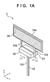
- FIG. 1A is a perspective view illustrating a first embodiment of the present invention.
- FIG. 1B is a diagram illustrating the first embodiment of the present invention.
- FIG. 1C is a plan view illustrating the first embodiment of the present invention.
- FIG. 2A is a plan view illustrating the function of the present invention.
- FIG. 2B shows plan views illustrating the function of the present invention.
- FIG. 2C shows plan views illustrating the function of the present invention.
- FIG. 3 is a graph illustrating drive signals of the present invention.
- FIG. 4 is a plan view illustrating another function of the present invention.
- FIG. 5A is a perspective view illustrating another configuration of the first embodiment of the present invention.
- FIG. 5B is a diagram illustrating the other configuration of the first embodiment of the present invention.
- FIG. 6A is a diagram illustrating another configuration of the first embodiment of the present invention.
- FIG. 6B is a diagram illustrating yet another configuration of the first embodiment of the present invention.
- FIG. 7 is a perspective view illustrating a second embodiment of the present invention.
- FIG. 8 is a graph illustrating a stress of the present invention.
- FIG. 9 is a perspective view illustrating Example 1 of the present invention.
- FIG. 10A is a perspective view illustrating Example 2 of the present invention.
- FIG. 10B is a perspective view illustrating Example 2 of the present invention.
- FIG. 11 is a perspective view illustrating Example 2 of the present invention.
- FIG. 12A is a plan view illustrating the function of the present invention.
- FIG. 12B is a plan view illustrating the function of the present invention.
- FIG. 12C is a plan view illustrating the function of the present invention.
- FIG. 13 is a graph illustrating drive signals of the present invention.
- FIG. 14 is a plan view illustrating an operation of an optical scanning device of the present invention.
- FIG. 15A is a graph illustrating an operation of the optical scanning device of the present invention.
- FIG. 15B is a graph illustrating an operation of the optical scanning device of the present invention.
- FIG. 15C is a graph illustrating an operation of the optical scanning device of the present invention.
- FIG. 16A is a graph illustrating an operation of the optical scanning device of the present invention.
- FIG. 16B is a graph illustrating an operation of the optical scanning device of the present invention.
- FIGS. 1A, 1B, and 1C show an optical scanning device 1 , serving as a vibrating mirror of a first embodiment of the present invention.
- the x-axis, y-axis, and z-axis are defined as shown in FIGS. 1A, 1B , and 1 C.
- a vibrating member 10 includes a torsion beam 101 , a mirror section 104 , and supporting sections 102 and 103 that support the mirror section 104 .
- the torsion beam may also be referred to as a gimbal, a hinge, or a torsion bar.
- the torsion beam 101 and the mirror section 104 are provided in one piece.
- the torsion beam 101 and the mirror section 104 are made from the same metal material.
- the upper parts of the supporting sections 102 and 103 are connected to the lower part of the mirror section 104 .
- the lower parts of the supporting sections 102 and 103 are connected to each other via a connection. Note that, in FIG. 1A , the connection is hidden since it is sandwiched between magnets 50 and 51 .
- the upper part of the torsion beam 101 is connected to the lower part of the connection.
- the mirror section 104 rotates around the torsion beam 101 that serves as the axis of rotation.
- the direction of the length of the torsion beam 101 is in parallel to the z-axis direction.
- a reflective film 20 is formed on a surface of the mirror section 104 as needed.
- the direction of the thickness of the mirror section 104 is in parallel to the y-axis direction. Also, the front and rear surfaces of the mirror section 104 are flat and in parallel to the x-axis direction. Note that, when the reflective film 20 is provided on the mirror section 104 , the surface of the reflective film 20 substantially serves as a mirror surface, and the mirror section 104 serves as a base body that is formed in one piece with the torsion beam 101 .
- the reflective film may be provided on one or both of the surfaces of the mirror section. In either case, by forming the torsion beam 101 and the mirror section 104 , serving as a variable focus mirror, in one piece, it is possible to downsize the entire device.
- the magnets 50 and 51 are arranged in the vicinity of the connection for the supporting sections 102 and 103 . That is, the magnets 50 and 51 are magnets that are mounted on the two supporting sections 102 and 103 .
- a driving coil 55 is a coil that is arranged corresponding to the magnets 50 and 51 , and generates a magnetic field upon application of an electric signal of a first frequency. Note that the magnetizing directions of the magnets 50 and 51 are the same.
- the magnetizing direction of the magnets 50 and 51 is a direction that is orthogonal to the z-axis direction of the torsion beam 101 (for example, the direction of an arrow D 1 or D 2 of FIG. 1A , or a direction opposite thereto).
- An electric signal is supplied to the driving coil 55 from a driving circuit 60 , and thereby the driving coil 55 generates a magnetic field. With this magnetic field, the magnets 50 and 51 attract or repel so as to induce torsional vibration to the torsion beam 101 .
- the torsional vibration of the torsion beam 101 rotates and vibrates the mirror section 104 . Therefore, the mirror section 104 changes (deviates) the direction of a light flux (laser light) that was output from a light source. Accordingly, optical scanning is realized by the mirror section 104 .
- a piezoelectric element 30 that changes the curvature of the mirror section 104 is arranged on the surface that is opposite to the mirror surface of the mirror section 104 , serving as the variable focus mirror.
- the piezoelectric element 30 functions as a second piezoelectric element that changes the curvature of the mirror surface upon application of an electric signal.
- FIG. 1C the mirror section 104 is subjected to bending deformation by the piezoelectric element 30 expanding and contracting depending on an electric signal (of a frequency f 2 and f 3 ) supplied from a driving circuit 61 .
- FIG. 1B shows the vibrating member 10 made from a metal material. Accordingly, the vibrating member 10 functions as an electrode or a wiring of the piezoelectric element 30 . Since the curvature of the surface of the mirror section 104 is changed due to this bending deformation caused by the piezoelectric element 30 , the mirror section 104 functions as a variable focus mirror.
- the present invention since an optical scanning mirror and a focus adjustment mirror are realized by the single mirror section 104 , serving as a variable focus mirror, the number of components can be reduced as compared with that of the conventional technique in which a vibrating mirror and a variable focus mirror are provided separately. That is, the present invention allows the provision of an optical scanning device that can be downsized by a reduction in number of components, and has an advantage in cost.
- the supporting sections 102 and 103 which extend from the connection that extends in two directions from the torsion beam 101 , are connected to the mirror section 104 .
- the supporting sections 102 and 103 function as two supporting sections that are arranged at two symmetrical positions with respect to the axis of rotation of the torsion beam 101 , and support the variable focus mirror. With this, even when a bending vibration is induced to the mirror section 104 , the gravity center of the mirror section 104 is not displaced.
- the vibrating member 10 has a one-piece structure, but may not necessarily have the one-piece structure.
- the vibrating member 10 having a one-piece structure is advantageous in terms of durability of the joint section, simplification of the manufacture processing, and a reduction in cost.
- the vibrating member 10 can be made from a metal material, a silicon wafer, a ceramic substrate, or the like. As a forming method, etching, press working, laser processing, wire electric discharge machining, or the like can be adopted. However, use of a metal material is advantageous in terms of impact resistance. This is because a metal material is not easily broken.
- a Co—Ni base alloy such as SPRON 510 manufactured by Seiko Instruments Inc. has a particularly high endurance limit.
- a Co—Ni base alloy is suitable for the optical scanning device 1 of the present invention to which a torsional stress and a bending stress are repeatedly applied.
- the reflective film 20 is made of, for example, a vapor-deposited film of Au, Ag, Al, or the like, and an enhanced reflective film may be formed as needed.
- the material of the magnets 50 and 51 is not particularly limited. However, when a magnet that is as small as possible and has a magnetic force as strong as possible is adopted, it is possible to reduce the moment of inertia caused by vibration. For example, an Nd—Fe—B base magnet or a Sm—Co base magnet that has a strong magnetic force, a Fe—Cr—Co base magnet whose shape can be downsized and that is excellent in workability or the like may be adopted.
- the material of the piezoelectric element 30 is not limited only to this.
- a material having a piezoelectric property such as barium titanate, lead titanate, or lead niobate, may be adopted.
- the piezoelectric element 30 is formed by adhesion of a sintered compact element or direct film formation.
- the piezoelectric element having a structure in which a sintered compact is stacked has an excellent property since it is largely displaced.
- direct film formation on the mirror section 104 of the vibrating member 10 is advantageous in terms of durability of the adhesion section.
- an aerosol deposition method and a gas deposition method have a high deposition rate, and can easily form a thick film having a good film quality.
- PZT is used for the material of the piezoelectric element 30 and a metal material is used for the vibrating member 10
- an improvement in piezoelectric property is achieved by forming an intermediate layer for preventing lead from diffusing.
- a high temperature can be set for a heat treatment. For example, an age-hardening treatment at about 500° C. to 600° C. can be performed on a Co—Ni base alloy.
- FIG. 2A is a plan view showing laser light scanning by the optical scanning device 1 , the optical scanning device 1 being viewed from above.
- laser light moves from the upper end of a surface P 1 to the middle, to the lower end thereof, to the middle, and to the upper end thereof, in this stated order.
- a distance from the laser light scanning center to the upper end of the surface P 1 is defined as R 1 ′
- the distance to the middle thereof is defined as R 1
- R 1′′ the distance to the lower end thereof
- R 2 ′ the distance from the laser light scanning center to the upper end of the surface P 2
- R 2 ′′ the distance to the middle thereof
- R 2 ′′ the distance to the lower end thereof.
- a barcode 90 is arranged in parallel to the surface P 1 and the surface P 2 at any position between the surface P 1 and the surface P 2 .
- FIG. 2B shows the state of the mirror section 104 when the upper end of the surface P 1 is scanned (hereinafter, referred to as a state (R 1 ′)), the state of the mirror section 104 when the middle of the surface P 1 is scanned (hereinafter, referred to as a state (R 1 )), and the state of the mirror section 104 when the lower end of the surface P 1 is scanned (hereinafter, referred to as a state (R 1 ′′)).
- FIG. 2C shows the state of the mirror section 104 when the upper end of the surface P 2 is scanned (hereinafter, referred to as a state (R 2 ′)), the state of the mirror section 104 when the middle of the surface P 2 is scanned (hereinafter, referred to as a state (R 2 )), and the state of the mirror section 104 when the lower end of the surface P 2 is scanned (hereinafter, referred to as a state (R 2 ′′)).
- the beam waist is located at the middle of the surface P 1 that is at the distance R 1 from the scanning center.
- the driving circuit 61 varies the electric signal that is applied to the piezoelectric element 30 so that the curvature of the mirror section 104 is 1/R 1 ′ and the radius of curvature is R 1 ′ (R 1 ⁇ R 1 ′). Accordingly, the radius of curvature is reduced from 1/R 1 to 1/R 1 ′, and the beam waist is located at the upper end of the surface P 1 that is at the distance R 1 ′ from the scanning center.
- the beam waist would be located at the distance R 1 from the scanning center, and thus the beam diameter increases at the upper end of the surface P 1 , resulting in a decrease in resolution and a deterioration in reading rate. Therefore, according to the present embodiment, when the upper end of the surface P 1 is scanned, the radius of curvature of the mirror section 104 is changed to R 1 ′ so that the beam waist is located on the surface P 1 .
- the beam waist is maintained on the surface P 1 by changing the radius of curvature to R 1 ′′ in the state (R 1 ′′) of FIG. 2B .
- an optical pattern such as the barcode 90 is disposed on the surface P 1 , it is possible to obtain the same resolution between the middle of the scan and the ends of the scan. Particularly, even when the scan angle is enlarged in order to cover a wide barcode, there is the effect that a significant improvement in reading rate is achieved.
- FIG. 2C shows the modified states of the mirror section 104 in which the beam waist is maintained on the surface P 2 .
- the beam waist is always maintained on the surface P 2 .
- by continuously moving the scan surface from the surface P 1 to the surface P 2 it is possible to reliably detect the barcode with a high resolution as long as it is positioned in the range from the surface P 1 to the surface P 2 . For example, a plurality of times of scanning are performed while moving the barcode from the surface P 1 to the surface P 2 , and the scanning results are decoded, and when an effective reading result has been obtained, the scanning may end.
- FIG. 3 shows examples of drive signals for performing scanning as shown in FIGS. 2A to 2C , the drive signals being generated by the driving circuits 60 and 61 .
- the driving circuits 60 and 61 serve as drive controllers that simultaneously generate a first drive signal for inducing torsional vibration to the torsion beam 101 and a second drive signal for inducing bending deformation to the variable focus mirror (mirror section 104 ).
- the driving circuits 60 and 61 are shown as separate circuits, and may be provided on individual substrates or a single substrate.
- the driving circuit 61 generates, as the second drive signal, a signal obtained by superimposing a plurality of frequencies that are different from the first frequency of the first drive signal that is output from the driving circuit 60 .
- the driving circuit 61 preferably generates, as the second drive signal, a signal including a signal of a frequency that corresponds to an even multiple of (e.g., two-times or four-times higher than) the first frequency. This is because efficient driving of the variable focus mirror can be realized.
- the driving circuit 61 preferably generates, as the second drive signal, a signal obtained by superimposing a signal having a frequency that is two times higher than the first frequency of the first drive signal, and a signal having a frequency that is four times higher than the first frequency. Note that the driving circuit 61 generates the second drive signal while generating the first drive signal, thereby making it possible to drive the variable focus mirror by an efficient operation.
- the driving circuit 60 serves as a first electric signal generation unit for generating a first electric signal of a first frequency so as to induce torsional vibration to the torsion beam 101 . That is, the driving circuit 60 outputs a first electric signal of a first frequency f 1 in order to induce rotational vibration to the mirror section 104 .
- the driving circuit 61 serves as a second electric signal generation unit that generates a second electric signal having a frequency that is an even multiple of (here, two-times higher than) the first frequency, and a third electric signal having a third frequency that is lower than the first frequency, so as to induce, to the variable focus mirror, a bending vibration that is obtained by superimposing deformation by the second electric signal and deformation by the electric signal of the third frequency.
- the driving circuit 61 outputs an electric signal that is obtained by superimposing the second electric signal, which has a second frequency f 2 that is two times higher than the first frequency f 1 , and the third electric signal, which has the third frequency f 3 that is sufficiently lower than the first frequency f 1 .
- the second electric signal is a signal for maintaining the beam waist always on the scan surface during one scanning.
- the third electric signal is a signal for continuously varying the distance from the scanning center to the scan surface.
- the number of times of scanning in a range from the surface P 1 to the surface P 2 increases as a difference between the frequency f 1 and the frequency f 3 is greater. Therefore, the focus accuracy is improved.
- a read time needed for bringing the barcode into focus and obtaining an effective signal is extended.
- the read time also depends on a time of one scanning, that is, the frequency of rotation of the mirror section 104 . For example, when reading in which the frequency of rotation of the mirror section 104 is in the range from 50 Hz to 100 Hz is performed within 0.2 second, the frequency f 3 is about 10 to 20 times higher than the frequency f 1 .
- the scan angle of the mirror section 104 is proportional to the amplitude of the drive signal of the frequency f 1 when the torsion beam 101 is used within an elastic range of the material of the torsion beam 101 . Furthermore, the mirror section 104 configures a unimorph-type piezoelectric vibrator to which the piezoelectric element 30 is adhered. Therefore, the magnitude of the curvature depends on the amplitude of a drive signal that is applied to the piezoelectric element 30 , the drive signal being obtained by synthesizing the frequency f 2 and the frequency f 3 .
- the magnitudes of bending deformation in the states (R 1 ′) and (R 1 ′′) of FIG. 2B are the same so that the distance from the scanning center to the beam waist is the same between the upper end and the lower end of the scan.
- the magnitudes of bending deformation in the states (R 1 ′) and (R 1 ′′) may also be different from each other, by adjusting the frequency of the drive signal that is applied to the piezoelectric element 30 by the driving circuit 61 . With this, it is possible to incline the scan surface on which the beam waist position is maintained as a surface P 1 ′ shown in FIG. 4 .
- this makes it possible to rotate the scan surface from the surface P 1 ′ to a surface P 1 ′′.
- the curvature of the mirror surface of the variable focus mirror is changed by the second electric signal and the third electric signal so that the beam waist of a light flux reflected by the mirror section 104 is located on the scan surface of the object being scanned that is an object on a plane.
- FIGS. 5A and 5B show an example of another configuration of the first embodiment of the present invention.
- An optical scanning device 2 differs from the optical scanning device shown in FIG. 1A in the rotational mechanism of the mirror section 104 .
- a connecting member 501 which is hidden in FIG. 1A , for connecting two supporting sections 102 and 103 is shown.
- the torsion beam 101 is constituted by two beams 11 and 12 , which extend from the connecting member 501 and are in parallel to each other.
- the beams 11 and 12 are respectively provided with piezoelectric elements 31 and 32 .
- the piezoelectric elements 31 and 32 are respectively provided on two beams 11 and 12 , and serve as first piezoelectric elements to which the first electric signal is applied.
- a driving circuit 62 shown in FIG. 5B applies an electric signal to the piezoelectric elements 31 and 32 so that the beams 11 and 12 are bent and deformed in opposite directions, thereby inducing rotational vibration to the mirror section 104 . Since the piezoelectric elements 31 and 32 can be formed similarly to the piezoelectric element 30 , it is possible to simplify the manufacturing process. Furthermore, since the magnets and the coil can be omitted, it is possible to achieve further downsizing by a reduction in number of components.
- a configuration in which a coil pattern is formed on the mirror section 104 , and a magnet is externally arranged may be used, the configuration inducing rotational vibration to the mirror section 104 by driving of a moving coil method.
- the mirror section 104 is supported on one side, a two-sided-supported configuration may be used in which the torsion beams and the supporting sections are provided on both sides of the mirror section 104 (the upper part and the lower part). The two-sided-supported configuration is advantageous in that falling of the mirror surface can be prevented.
- FIGS. 6A and 6B show examples of other configurations of the piezoelectric element 30 .
- FIG. 6A shows the configuration in which a plurality of piezoelectric elements 33 that have the same shape are arranged on the rear surface of the mirror section 104 at substantially the same distance apart.
- the driving circuit 60 applying different driving voltages to the respective piezoelectric elements 33 , it is possible to form a curvature distribution of the mirror surface and to perform spherical aberration correction. That is, the variation width of the curvature of the mirror surface is limited when only one piezoelectric element is used, but a curvature distribution can freely be formed when a plurality of piezoelectric elements are used, making aberration correction easy.
- the drive signals that are applied to the plurality of piezoelectric elements 33 have different amplitudes, but may have the same phase and frequency.
- FIG. 6B shows the configuration in which a plurality of uniform piezoelectric elements 34 are arranged at a different distance apart at the ends from those in the middle of the back surface of the mirror surface.
- the driving circuit 60 applies the same voltage to the plurality of piezoelectric elements 34 , but the amount of bending deformation of the mirror section 104 is different depending on the position thereof. This is because the distances between the plurality of piezoelectric elements 34 are different between the ends and the middle of the mirror section 104 . That is, drive signals that have, in all respects, the same amplitude as well as the same phase and frequency are supplied to the plurality of piezoelectric elements 34 .
- the piezoelectric elements 33 and 34 function as second piezoelectric elements for varying the curvature of the mirror surface.
- FIG. 7 The configuration of FIG. 7 is similar to the configuration shown in FIG. 5A , but differs therefrom in that the mirror section 104 is already curved without any voltage being applied to the piezoelectric element 30 .
- a processing for forming a curvature of the mirror section 104 mechanical bending processing, thermal bending processing using a laser, or the like may be adopted.
- a metal material is used for the vibrating member 10 .
- a metal glass may be used for the metal material. By performing bending processing on the metal glass in a supercooled region, it is possible to make formation of a curvature and formation of a mirror surface by transfer of the mold at the same time.
- the reflective film 20 is not necessary.
- Giving a curvature to the mirror section 104 may be performed using a roller at the same time as metal rolling if the mirror section 104 is made from a metal material.
- the piezoelectric element 30 may also be formed by direct film deposition.
- FIG. 8 is a diagram illustrating a stress change when the mirror section 104 is repeatedly bent and deformed.
- the mirror section 104 is not deformed in advance (that is, when the mirror surface is flat while a voltage is not applied to the piezoelectric element 30 )
- an offset voltage for obtaining a minimum required curvature is applied to the piezoelectric element 30 , and then an electric signal obtained by superimposing the second frequency f 2 and the third frequency f 3 shown in FIG. 3 is applied.
- a change in stress that is applied to the joint surfaces of the piezoelectric element 30 and the mirror section 104 is offset as indicated by ⁇ 1 of FIG. 8 , and thus the maximum stress that is to be applied to the mirror section 104 is very large. This may cause a problem that the piezoelectric element 30 is detached due to repeated deformation, for example.
- the maximum stress can relatively be reduced since a change in stress that is applied to the joint surfaces of the piezoelectric element 30 and the mirror section 104 varies equally between the positive and the negative as indicated by ⁇ 2 of FIG. 8 . Accordingly, the problem that the piezoelectric element 30 is detached, for example, is not likely to occur even in the case of repeated deformation, and thus it is possible to realize a highly reliable optical scanning device 3 .
- the torsion beams 11 and 12 and the mirror section 104 serving as a variable focus mirror, from a metal material, and configuring the mirror surface of the mirror section 104 that is bent and deformed in a state in which none of the first electric signal, the second electric signal, and the third electric signal is generated, it is possible to improve the durability of the optical scanning device.
- FIG. 9 shows an image reading system 5 according to an example.
- the optical scanning device 3 shown in FIG. 7 is used as an optical scanning device, but either one of the optical scanning devices 1 and 2 may be used.
- As a material of the vibrating member 10 SPRON 510 (manufactured by Seiko Instruments Inc.) of Co—Ni—Cr—Mo alloy is used, and the vibrating member 10 is formed by wire cut processing.
- As the piezoelectric element 30 that is arranged on the rear surface of the mirror section 104 a PZT film that is formed by an aerosol deposition method is used.
- laser light output from a laser light source 70 is reflected by the optical scanning device 3 , and scans the barcode 90 , serving as an object to be scanned, that is arranged on the scan surface.
- the beam waist of the laser light is always maintained on the barcode.
- a driving circuit 63 outputs the above-described first to third drive signals. Scattered light from the barcode 90 , which is reflected light from the object being scanned, is collected on a photosensor 80 via a collecting lens 35 , which is a light collecting member for collecting scattered light, and is detected by the photosensor 80 .
- the photosensor 80 functions as a light receiving element for receiving the reflected light collected by the light collecting member.
- a signal processing circuit 64 converts an analog signal that is output from the photosensor 80 into a digital signal, generates an image signal that corresponds to the barcode 90 , and outputs the generated signal to a decoder 65 .
- the decoder 65 decodes the barcode 90 based on the image signal. Since the image reading system 5 of the present example uses the optical scanning device 3 of the present invention, the image reading system 5 can detect even a high-resolution wide pattern, with a high resolution, and can be downsized.
- FIGS. 10A and 10B show an example of an optical scanning device of the present invention.
- An optical scanning device 4 adopts a two-sided-supported configuration in which torsion beams 101 and 107 are provided on two sides, the configuration being developed from the configuration of FIGS. 1A to 1C .
- An outer mirror 108 for efficiently detecting return light from an optical pattern is provided.
- a coil pattern 56 is formed on the rear surface of the outer mirror 108 , and magnets 52 and 53 are provided outside the outer mirror 108 . That is, the optical scanning device 4 adopts a configuration for inducing torsional vibration by a moving coil method.
- the coil pattern 56 functions as a coil that is arranged corresponding to the magnets 52 and 53 , and generates a magnetic field upon application of an electric signal of a first frequency.
- the magnetizing directions of the magnets 52 and 53 are parallel to the magnetic field generated by the coil pattern 56 . That is, the magnetizing directions of the magnets 52 and 53 only need to be the direction of the arrow D 1 or the opposite direction. With this, a rotational torque is generated.
- a reflective film 21 is formed on the surface of the outer mirror 108 so as to increase the reflection ratio.
- a space is formed in the middle of the outer mirror 108 , and the mirror section 104 is arranged in this space.
- the mirror section 104 is connected to the outer mirror 108 by four supporting sections 102 , 103 , 105 , and 106 .
- the supporting sections 105 and 106 are connected to the upper part of the mirror section 104
- the supporting sections 102 and 103 are connected to the lower part of the mirror section 104 .
- the supporting sections 102 , 103 , 105 , and 106 are arranged at positions of the mirror section 104 that are not displaced in the y-axis direction at the time of the bending vibration.
- FIG. 11 shows an image reading system 6 , which is an example using the optical scanning device 4 of FIG. 10A .
- Laser light L 1 that was emitted from the laser light source 70 is reflected on the mirror section 104 , and scans the barcode 90 .
- Scattered light L 2 from the barcode 90 is reflected on the outer mirror 108 , and travels to a light collecting mirror 36 , which is a light collecting member.
- the scattered light L 2 is collected by the light collecting mirror 36 , and enters the photosensor 80 .
- the outer mirror 108 selectively reflects, on the light collecting mirror 36 , only the scattered light L 2 in the direction in which the laser light L 1 has been projected, making it possible to further improve the detection accuracy.
- the size of the image reading system 6 is larger than the size of the image reading system 5 shown in FIG. 9 , but the image reading system 6 can realize an image reading system that has a high reading rate even with respect to a high-resolution wide pattern, due to an interactive effect of a high resolution by displacing the beam waist position of the laser light L 1 , and an improvement in detection accuracy using direction selective detection.
- FIG. 12A shows a state of laser light scanning by the optical scanning device according to the present invention. Furthermore, FIG. 12B shows aspects of deformation of the mirror member 104 that is arranged on the vibrating member 10 , which serves as a rotating and vibrating body. This deformation is the same in an optical scanning direction and a sub-scanning direction that is perpendicular thereto.
- the beam waist is located in the middle of the projection surface P 1 that is at the distance R 1 from the scanning center.
- the curvature of the mirror member 104 decreases from that of the state R 1 due to the change in the electric signal that is applied to the piezoelectric material.
- the beam waist is located at the right end of the projection surface P 1 that is at the distance R 1 ′ from the scanning center.
- the beam waist would be located at the distance R 1 in the direction to the end of scan, and the beam diameter would be extended on the right end of the projection surface P 1 .
- the beam waist is maintained on the projection surface P 1 by changing the curvature in the state R′′ of FIG. 12B .
- control for changing mirror curvature two times during one reciprocation scan may be performed, that is, the mirror curvature is controlled using a signal having a frequency that is two times higher than a scan frequency.
- FIG. 12C shows the modified state of the mirror member 104 for maintaining the beam waist on the projection surface P 2 that has a longer projection distance than that of the surface P 1 .
- the beam waist position is shifted from R 2 , to R 2 ′, to R 2 , to R 2 ′′, and to R 2 , in the stated order. Accordingly, it is also possible to change the surface on which the beam waist is maintained by controlling a drive signal of the piezoelectric material.
- FIG. 13 shows examples of drive signals for performing scanning as shown in FIGS. 12A to 12C .
- the driving circuit 60 for inducing rotational vibration to the rotating and vibrating body applies a drive signal of the frequency f 1
- the driving circuit 61 for inducing curvature deformation to the mirror member 104 applies a signal obtained by adding an offset voltage ⁇ V to a drive signal of the frequency f 2 that is two times higher than the frequency f 1
- the drive signal of the frequency f 2 is a signal component for maintaining the beam waist on the scan surface during one scanning.
- ⁇ V is a signal component for changing the surface on which the beam waist is maintained.
- the phases of the drive signal f 1 and the rotation angle of the mirror are shifted by 90 degrees, and thus the phase of the drive signal of the frequency f 2 is shifted from the phase of the drive signal of the frequency f 1 so that the curvature deformation of the mirror is controlled depending on the rotation angle.
- the beam intensity is varied based on time-series data while the beam is scanned, or a change in intensity of reflected light during beam scanning is detected as time-series data.
- image formation and projection, reading of an optical pattern, and the like are performed.
- a distortion of the image or a change in reading resolution may be caused.
- a method for correcting the time-series data so that a change in beam intensity corresponds to a change in moving speed of the beam, and a method for letting the reading speed correspond to the change in moving speed are also considered.
- these methods need expensive controlling means that operates with a high speed.
- the beam spot is required to move on the projection surface with a speed that is as constant as possible.
- the scan angle of the beam of the vibrating mirror varies in the shape of a sine curve, but, among them, a scan angle that is in a range in which a constant speed is obtained on the projection surface may be used.
- FIG. 14 shows the state of optical scanning.
- the maximum scan angle of the beam due to rotational vibration of the mirror member 104 is defined as ⁇ o.
- An effective range in which scan light is actually used, of the maximum scan angle, is defined as ⁇ eff.
- the range that corresponds to ⁇ eff on a projection surface P located at the distance L from the scanning center is defined as Xeff.
- the position of Xeff corresponds to the position of R 1 ′ that is at the end of the projection surface P 1 .
- the beam direction is the direction of angle ⁇ .
- the moving speed of the beam spot formed on the projection surface P is V
- the change rate V/Vo of the moving speed V with respect to the angle ⁇ is as shown in FIG. 15A .
- the horizontal axis shows an angle ⁇ that indicates the beam direction
- the vertical axis shows the change rate V/Vo of the moving speed V.
- the angle in this range of the graph iii that is, the effective scan angle ⁇ eff is ⁇ 3 .
- the effective scan angle extends to ⁇ 4 .
- the effective scan angle is ⁇ 5 and thus smaller than ⁇ 4 . Therefore, even by increasing the maximum scan angle ⁇ o as compared with ⁇ 4 , it is not possible to extend the effective scan angle ⁇ eff.
- FIG. 15B shows the relationship between the maximum scan angle ⁇ o and the effective scan angle ⁇ eff. According to FIG. 15B , the maximum scan angle in which the effective scan angle ⁇ eff is the largest differs depending on the magnitude of the allowable error ⁇ v.
- FIG. 15C shows the maximum effective scan angle ⁇ eff with respect to the magnitude of the allowable error ⁇ v, and the maximum scan angle ⁇ o that is needed for obtaining the maximum effective scan angle ⁇ eff.
- the maximum scan angle ⁇ o of at least 40 degree is needed, although there is a difference due to the allowable error ⁇ v.
- the effective scan angle ⁇ eff is set as wide as possible.
- the maximum scan angle ⁇ eff may also be set as narrow as possible in view of downsizing of the vibrating mirror or power consumption.
- the vibrating mirror is operated at the maximum scan angle ⁇ o at which the effective scan angle ⁇ eff achieves a peak. Accordingly, it is also possible to set a maximum scan angle with respect to the scanning center to ⁇ 40 degrees or more, and a rotational vibration amplitude of the vibrating mirror to ⁇ 20 degrees or more.
- the torsion beam 101 that supports the mirror needs to have a high strength and durability.
- an age-hardening Co—Ni base alloy may be used as a material of the torsion beam 101 .
- the diameter of the beam spot largely affects the resolution of an image that is formed or projected by optical scanning, or the reading resolution of an optical pattern. Therefore, a change in diameter of the beam spot within the effective scan region may be reduced as much as possible.
- FIG. 16A shows an example of a change in diameter of the beam spot at a position on the projection surface.
- FIG. 16A shows a change in diameter of the beam spot when, in FIG. 14 , the projection distance L is set to 174 mm, and the beam spot is moved from the middle O of the projection surface in the x-axis direction by rotational vibration of the vibrating mirror.
- the horizontal axis shows a distance from the middle of the projection surface
- the vertical axis shows the diameter of the beam spot.
- FIG. 16B shows examples of drive signals that are applied to the piezoelectric material in order to change the curvature of the mirror member 104 .
- the drive signal of the frequency f 2 is a signal having the frequency of rotational vibration of the vibrating mirror, that is, a frequency that is two times higher than the scan frequency f 1 . This is the same signal as the drive signal of the frequency f 2 shown in FIG. 13 .
- the drive signal of the frequency f 4 is a signal having a frequency that is four times higher than the frequency f 1 .
- the drive signal of the frequency f 2 +f 4 is a signal generated by superimposing the drive signal of the frequency f 2 and the drive signal of the frequency f 4 in an appropriate proportion.
- the diameter of the beam spot when the curvature of the mirror member 104 is varied by the drive signal of the frequency f 2 is shown by the graph “only f 2 ” of FIG. 16A .
- the diameter of the beam spot when the curvature of the mirror member 104 is varied by the drive signal obtained by superimposing the drive signals of frequencies f 2 and f 4 is shown by the graph “f 2 +f 4 ” of FIG. 16A . It is possible to obtain a substantially constant diameter of the beam spot irrespective of the position.
- the above-described effects of constant speed characteristics or the stabilized diameter of the beam spot can be obtained when the vibrating mirror can perform stable optical scanning without causing abnormal vibration or the like.
- the vibrating mirror of the present invention may be used to appropriately set the maximum scan angle, and to control the curvature of the mirror with drive signals having frequencies that are two and four times higher than the scan frequency. Accordingly, it is possible to realize an optical scanning device that can perform image formation and projection, reading of an optical pattern, and the like with high accuracy.
- the optical scanning device 1 according to the present embodiment is applicable to the above-described image reading device of Example 1 and the image reading system of Example 2, achieving the same effects as those of the above-described other embodiments. Furthermore, the present invention is also applicable to an image forming device or an image projecting device.
Landscapes
- Physics & Mathematics (AREA)
- General Physics & Mathematics (AREA)
- Optics & Photonics (AREA)
- Electromagnetism (AREA)
- Mechanical Optical Scanning Systems (AREA)
- Mechanical Light Control Or Optical Switches (AREA)
- Mounting And Adjusting Of Optical Elements (AREA)
- Facsimile Scanning Arrangements (AREA)
Applications Claiming Priority (3)
| Application Number | Priority Date | Filing Date | Title |
|---|---|---|---|
| JP2012-098229 | 2012-04-23 | ||
| JP2012098229 | 2012-04-23 | ||
| PCT/JP2013/002720 WO2013161271A1 (ja) | 2012-04-23 | 2013-04-23 | 光走査装置及び画像読取装置 |
Related Parent Applications (1)
| Application Number | Title | Priority Date | Filing Date |
|---|---|---|---|
| PCT/JP2013/002720 Continuation WO2013161271A1 (ja) | 2012-04-23 | 2013-04-23 | 光走査装置及び画像読取装置 |
Publications (2)
| Publication Number | Publication Date |
|---|---|
| US20150036202A1 US20150036202A1 (en) | 2015-02-05 |
| US9664899B2 true US9664899B2 (en) | 2017-05-30 |
Family
ID=49482614
Family Applications (1)
| Application Number | Title | Priority Date | Filing Date |
|---|---|---|---|
| US14/517,529 Expired - Fee Related US9664899B2 (en) | 2012-04-23 | 2014-10-17 | Optical scanning device and image reading system |
Country Status (3)
| Country | Link |
|---|---|
| US (1) | US9664899B2 (ja) |
| JP (1) | JP5952391B2 (ja) |
| WO (1) | WO2013161271A1 (ja) |
Families Citing this family (9)
| Publication number | Priority date | Publication date | Assignee | Title |
|---|---|---|---|---|
| JP6224432B2 (ja) * | 2013-11-19 | 2017-11-01 | キヤノン電子株式会社 | 振動装置、光走査装置、それを用いた画像形成装置および映像投射装置 |
| JP6231361B2 (ja) * | 2013-11-25 | 2017-11-15 | キヤノン電子株式会社 | 振動素子および光走査装置 |
| JP6301184B2 (ja) * | 2014-04-28 | 2018-03-28 | キヤノン電子株式会社 | 振動素子、光走査装置、画像形成装置、画像投影装置および光学パターン読み取り装置 |
| JP6350057B2 (ja) * | 2014-07-16 | 2018-07-04 | 株式会社デンソー | 光走査装置 |
| JP6451115B2 (ja) * | 2014-07-16 | 2019-01-16 | 株式会社デンソー | 光走査装置 |
| JP6442919B2 (ja) * | 2014-08-21 | 2018-12-26 | 株式会社デンソー | 光走査装置 |
| JP6862154B2 (ja) * | 2016-11-22 | 2021-04-21 | キヤノン株式会社 | 光学素子、露光装置、および物品の製造方法 |
| DE102017002862A1 (de) * | 2017-03-24 | 2018-09-27 | Blickfeld GmbH | Winkelmagnetfeldsensor für Scanner |
| GB202101833D0 (en) * | 2021-02-10 | 2021-03-24 | Sintef Tto As | Actuating device |
Citations (10)
| Publication number | Priority date | Publication date | Assignee | Title |
|---|---|---|---|---|
| JPS6333060A (ja) | 1986-07-25 | 1988-02-12 | Konica Corp | 画像情報読取装置 |
| JPH07121645A (ja) | 1993-09-02 | 1995-05-12 | Nippondenso Co Ltd | 光学的情報読取装置 |
| US5498868A (en) | 1993-09-02 | 1996-03-12 | Nippondenso Co., Ltd. | Optical data reader capable of quickly changing a condensing position of a light beam |
| WO1999045441A1 (en) | 1998-03-02 | 1999-09-10 | Micronic Laser Systems Ab | Improved modulator design for pattern generator |
| JP2001013428A (ja) | 1999-06-28 | 2001-01-19 | Seiko Epson Corp | 光変調デバイス及び表示装置 |
| JP2001100119A (ja) | 1999-09-30 | 2001-04-13 | Seiko Epson Corp | 光変調デバイス及び表示装置 |
| JP2006084495A (ja) | 2004-09-14 | 2006-03-30 | Nippon Signal Co Ltd:The | 可変焦点型光学装置 |
| US20090021818A1 (en) * | 2007-07-20 | 2009-01-22 | Ethicon Endo-Surgery, Inc. | Medical scanning assembly with variable image capture and display |
| JP2010008543A (ja) | 2008-06-25 | 2010-01-14 | Panasonic Corp | 光走査装置 |
| JP2012242685A (ja) | 2011-05-20 | 2012-12-10 | Canon Electronics Inc | 光走査装置及び光学パターン読取装置 |
-
2013
- 2013-04-23 JP JP2014512353A patent/JP5952391B2/ja not_active Expired - Fee Related
- 2013-04-23 WO PCT/JP2013/002720 patent/WO2013161271A1/ja not_active Ceased
-
2014
- 2014-10-17 US US14/517,529 patent/US9664899B2/en not_active Expired - Fee Related
Patent Citations (12)
| Publication number | Priority date | Publication date | Assignee | Title |
|---|---|---|---|---|
| JPS6333060A (ja) | 1986-07-25 | 1988-02-12 | Konica Corp | 画像情報読取装置 |
| JPH07121645A (ja) | 1993-09-02 | 1995-05-12 | Nippondenso Co Ltd | 光学的情報読取装置 |
| US5498868A (en) | 1993-09-02 | 1996-03-12 | Nippondenso Co., Ltd. | Optical data reader capable of quickly changing a condensing position of a light beam |
| WO1999045441A1 (en) | 1998-03-02 | 1999-09-10 | Micronic Laser Systems Ab | Improved modulator design for pattern generator |
| US6285488B1 (en) | 1998-03-02 | 2001-09-04 | Micronic Laser Systems Ab | Pattern generator for avoiding stitching errors |
| JP2002506236A (ja) | 1998-03-02 | 2002-02-26 | マイクロニック レーザー システムズ アクチボラゲット | 変調装置の設計を改良したパターン・ジェネレータ |
| JP2001013428A (ja) | 1999-06-28 | 2001-01-19 | Seiko Epson Corp | 光変調デバイス及び表示装置 |
| JP2001100119A (ja) | 1999-09-30 | 2001-04-13 | Seiko Epson Corp | 光変調デバイス及び表示装置 |
| JP2006084495A (ja) | 2004-09-14 | 2006-03-30 | Nippon Signal Co Ltd:The | 可変焦点型光学装置 |
| US20090021818A1 (en) * | 2007-07-20 | 2009-01-22 | Ethicon Endo-Surgery, Inc. | Medical scanning assembly with variable image capture and display |
| JP2010008543A (ja) | 2008-06-25 | 2010-01-14 | Panasonic Corp | 光走査装置 |
| JP2012242685A (ja) | 2011-05-20 | 2012-12-10 | Canon Electronics Inc | 光走査装置及び光学パターン読取装置 |
Non-Patent Citations (1)
| Title |
|---|
| JPO Office Action dated Oct. 9, 2015 in counterpart Japanese Patent Application No. 2014-512353, together with partial English language translation. |
Also Published As
| Publication number | Publication date |
|---|---|
| WO2013161271A1 (ja) | 2013-10-31 |
| US20150036202A1 (en) | 2015-02-05 |
| JP5952391B2 (ja) | 2016-07-13 |
| JPWO2013161271A1 (ja) | 2015-12-21 |
Similar Documents
| Publication | Publication Date | Title |
|---|---|---|
| US9664899B2 (en) | Optical scanning device and image reading system | |
| US7436567B2 (en) | Optical scanner and scanning type projector | |
| US8395834B2 (en) | Deflecting mirror for deflecting and scanning light beam | |
| JP4277921B2 (ja) | アクチュエータ、光スキャナおよび画像形成装置 | |
| US20100309536A1 (en) | Optical deflector, optical scanner, image forming apparatus, and image projector | |
| JP2008139886A (ja) | 2次元マイクロ光スキャナー | |
| JP2005128147A (ja) | 光偏向器及び光学装置 | |
| JP2008170565A (ja) | 揺動体装置、及び揺動体装置を用いた画像形成装置 | |
| JP2008076696A (ja) | アクチュエータ、光スキャナおよび画像形成装置 | |
| JP5170983B2 (ja) | 光偏向器、及びそれを用いた光学機器 | |
| JP2015210451A (ja) | 振動素子、光走査装置、画像形成装置、画像投影装置および光学パターン読み取り装置 | |
| JP2009198702A (ja) | 揺動構造体、及び揺動構造体を用いた揺動体装置 | |
| JP4620789B1 (ja) | 光走査装置 | |
| JP2015210450A (ja) | 振動素子、光走査装置、画像形成装置、画像投影装置および光学パターン読み取り装置 | |
| JP2008111882A (ja) | アクチュエータ、光スキャナおよび画像形成装置 | |
| JP2016114715A (ja) | 振動素子、光走査装置、画像形成装置、画像投影装置および画像読み取り装置 | |
| US8717653B2 (en) | Light scanner and image forming apparatus | |
| JP2006084495A (ja) | 可変焦点型光学装置 | |
| JP2016012023A (ja) | 振動素子および光走査装置 | |
| JP6231361B2 (ja) | 振動素子および光走査装置 | |
| JP2015210452A (ja) | 光走査装置、画像形成装置、画像投影装置および読み取り装置 | |
| JP2013225081A (ja) | 光走査装置及び画像形成装置 | |
| JPH08122679A (ja) | 光走査用アクチュエータ | |
| JP6301184B2 (ja) | 振動素子、光走査装置、画像形成装置、画像投影装置および光学パターン読み取り装置 | |
| JP2015210449A (ja) | 振動素子、光走査装置、画像形成装置、画像投影装置および光学パターン読み取り装置 |
Legal Events
| Date | Code | Title | Description |
|---|---|---|---|
| AS | Assignment |
Owner name: CANON DENSHI KABUSHIKI KAISHA, JAPAN Free format text: ASSIGNMENT OF ASSIGNORS INTEREST;ASSIGNORS:SUZUKI, NARUKI;WAKABAYASHI, TAKAYUKI;ARAI, KATSUMI;REEL/FRAME:033986/0348 Effective date: 20141016 |
|
| STCF | Information on status: patent grant |
Free format text: PATENTED CASE |
|
| MAFP | Maintenance fee payment |
Free format text: PAYMENT OF MAINTENANCE FEE, 4TH YEAR, LARGE ENTITY (ORIGINAL EVENT CODE: M1551); ENTITY STATUS OF PATENT OWNER: LARGE ENTITY Year of fee payment: 4 |
|
| FEPP | Fee payment procedure |
Free format text: MAINTENANCE FEE REMINDER MAILED (ORIGINAL EVENT CODE: REM.); ENTITY STATUS OF PATENT OWNER: LARGE ENTITY |
|
| LAPS | Lapse for failure to pay maintenance fees |
Free format text: PATENT EXPIRED FOR FAILURE TO PAY MAINTENANCE FEES (ORIGINAL EVENT CODE: EXP.); ENTITY STATUS OF PATENT OWNER: LARGE ENTITY |
|
| STCH | Information on status: patent discontinuation |
Free format text: PATENT EXPIRED DUE TO NONPAYMENT OF MAINTENANCE FEES UNDER 37 CFR 1.362 |
|
| FP | Lapsed due to failure to pay maintenance fee |
Effective date: 20250530 |