US9602713B2 - Imaging apparatus and method for controlling the same - Google Patents
Imaging apparatus and method for controlling the same Download PDFInfo
- Publication number
- US9602713B2 US9602713B2 US14/217,795 US201414217795A US9602713B2 US 9602713 B2 US9602713 B2 US 9602713B2 US 201414217795 A US201414217795 A US 201414217795A US 9602713 B2 US9602713 B2 US 9602713B2
- Authority
- US
- United States
- Prior art keywords
- image
- signal
- imaging apparatus
- image signal
- image sensor
- Prior art date
- Legal status (The legal status is an assumption and is not a legal conclusion. Google has not performed a legal analysis and makes no representation as to the accuracy of the status listed.)
- Active
Links
Images


Classifications
-
- H04N5/23212—
-
- H—ELECTRICITY
- H04—ELECTRIC COMMUNICATION TECHNIQUE
- H04N—PICTORIAL COMMUNICATION, e.g. TELEVISION
- H04N23/00—Cameras or camera modules comprising electronic image sensors; Control thereof
- H04N23/60—Control of cameras or camera modules
- H04N23/67—Focus control based on electronic image sensor signals
- H04N23/673—Focus control based on electronic image sensor signals based on contrast or high frequency components of image signals, e.g. hill climbing method
-
- H—ELECTRICITY
- H04—ELECTRIC COMMUNICATION TECHNIQUE
- H04N—PICTORIAL COMMUNICATION, e.g. TELEVISION
- H04N23/00—Cameras or camera modules comprising electronic image sensors; Control thereof
- H04N23/60—Control of cameras or camera modules
- H04N23/67—Focus control based on electronic image sensor signals
-
- H—ELECTRICITY
- H04—ELECTRIC COMMUNICATION TECHNIQUE
- H04N—PICTORIAL COMMUNICATION, e.g. TELEVISION
- H04N25/00—Circuitry of solid-state image sensors [SSIS]; Control thereof
- H04N25/10—Circuitry of solid-state image sensors [SSIS]; Control thereof for transforming different wavelengths into image signals
- H04N25/11—Arrangement of colour filter arrays [CFA]; Filter mosaics
- H04N25/13—Arrangement of colour filter arrays [CFA]; Filter mosaics characterised by the spectral characteristics of the filter elements
- H04N25/134—Arrangement of colour filter arrays [CFA]; Filter mosaics characterised by the spectral characteristics of the filter elements based on three different wavelength filter elements
-
- H—ELECTRICITY
- H04—ELECTRIC COMMUNICATION TECHNIQUE
- H04N—PICTORIAL COMMUNICATION, e.g. TELEVISION
- H04N25/00—Circuitry of solid-state image sensors [SSIS]; Control thereof
- H04N25/60—Noise processing, e.g. detecting, correcting, reducing or removing noise
- H04N25/61—Noise processing, e.g. detecting, correcting, reducing or removing noise the noise originating only from the lens unit, e.g. flare, shading, vignetting or "cos4"
-
- H—ELECTRICITY
- H04—ELECTRIC COMMUNICATION TECHNIQUE
- H04N—PICTORIAL COMMUNICATION, e.g. TELEVISION
- H04N25/00—Circuitry of solid-state image sensors [SSIS]; Control thereof
- H04N25/70—SSIS architectures; Circuits associated therewith
- H04N25/703—SSIS architectures incorporating pixels for producing signals other than image signals
- H04N25/704—Pixels specially adapted for focusing, e.g. phase difference pixel sets
-
- H04N5/3572—
-
- H—ELECTRICITY
- H10—SEMICONDUCTOR DEVICES; ELECTRIC SOLID-STATE DEVICES NOT OTHERWISE PROVIDED FOR
- H10F—INORGANIC SEMICONDUCTOR DEVICES SENSITIVE TO INFRARED RADIATION, LIGHT, ELECTROMAGNETIC RADIATION OF SHORTER WAVELENGTH OR CORPUSCULAR RADIATION
- H10F39/00—Integrated devices, or assemblies of multiple devices, comprising at least one element covered by group H10F30/00, e.g. radiation detectors comprising photodiode arrays
- H10F39/80—Constructional details of image sensors
- H10F39/805—Coatings
- H10F39/8057—Optical shielding
-
- H—ELECTRICITY
- H10—SEMICONDUCTOR DEVICES; ELECTRIC SOLID-STATE DEVICES NOT OTHERWISE PROVIDED FOR
- H10F—INORGANIC SEMICONDUCTOR DEVICES SENSITIVE TO INFRARED RADIATION, LIGHT, ELECTROMAGNETIC RADIATION OF SHORTER WAVELENGTH OR CORPUSCULAR RADIATION
- H10F39/00—Integrated devices, or assemblies of multiple devices, comprising at least one element covered by group H10F30/00, e.g. radiation detectors comprising photodiode arrays
- H10F39/80—Constructional details of image sensors
- H10F39/806—Optical elements or arrangements associated with the image sensors
- H10F39/8063—Microlenses
Definitions
- the present disclosure relates to an imaging apparatus and a method for controlling the imaging apparatus.
- the present disclosure also relates to a technique for obtaining a pupil division image using an image sensor configured of a microlens corresponding to a plurality of photoelectric conversion units, and more particularly to a technique for preferably correcting distortion of an image caused by saturation occurring in each of the photoelectric conversion units of a pixel.
- Japanese Patent Application Laid-Open No. 2001-83407 discusses a technique for generating a view image by a conventional signal processing technique, in which focus detection is performed by acquiring a phase difference of pupil-divided images while all values of photoelectric conversion units corresponding to the same microlens are added up to treat that addition value as a value of one pixel so that the pixel array thereof is the same as that of the conventional imaging pixel.
- an analog-digital (AD) converter exceeds its conversion range to reach the apparent saturation level.
- An amount of electric charges that can be stored in the division pixel as the addition value thereof is up to twice as much as the amount of AD conversion range. In such a state, even if a value of one division pixel is subtracted from an addition value of the division pixels, a value of another division pixel cannot be restored.
- the present disclosure is directed to an imaging apparatus capable of performing focus detection with respect to a saturated signal.
- an imaging apparatus includes: an image sensor configured of an imaging pixel having a plurality of photoelectric conversion units; and a focus adjustment unit which performs a phase-difference detection type focus adjustment using a pair of image signals detected by a plurality of the photoelectric conversion units.
- the imaging apparatus includes a subtraction unit and a suppression unit. One signal of a pair of the image signals is a first image signal whereas the other signal of a pair of the image signals is a second image signal.
- the subtraction unit generates the second image signal by subtracting the first image signal, that is output from the image sensor, from an addition signal that is acquired by adding the first image signal and the second image signal output from the image sensor, and the suppression unit suppresses the first image signal to a value equal to or less than a predetermined value.
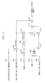
- FIG. 1 is a block diagram illustrating a focus detection pixel separation unit according to an exemplary embodiment of the present invention.
- FIG. 2 is a cross-sectional view of an image sensor according to the exemplary embodiment of the present invention.
- FIGS. 3A and 3B are graphs illustrating output characteristics of incident light according to the exemplary embodiment of the present invention.
- FIG. 4 is a timing chart of respective portions according to the exemplary embodiment of the present invention.
- FIG. 5 is an area divisional diagram of the image sensor according to the exemplary embodiment of the present invention.
- FIG. 6 is a block diagram illustrating an imaging apparatus according to a first exemplary embodiment of the present invention.
- FIGS. 7A through 7C are waveform charts illustrating respective portions of signals according to the exemplary embodiment of the present invention.
- FIG. 8 is a flowchart of a program for focus detection pixel separation processing according to a second exemplary embodiment of the present invention.
- FIGS. 9A and 9B are waveform charts illustrating signal waveforms of images A, A+B, and B according to third and fourth exemplary embodiments of the present invention.
- FIGS. 10A through 10C are graphs illustrating output characteristics of incident light according to the third exemplary embodiment of the present invention.
- FIG. 11 is a circuit block diagram according to the third exemplary embodiment of the present invention.
- FIG. 12 is a schematic diagram of an image-forming surface, illustrating refocusing processing according to a fifth exemplary embodiment of the present invention.
- FIGS. 13A and 13B are diagrams illustrating shading characteristics according to a sixth exemplary embodiment of the present invention.
- FIG. 14 is a front view illustrating an imaging plane of the image sensor according to the sixth exemplary embodiment of the present invention.
- FIGS. 15A through 15C are principle diagrams of imaging plane phase-difference autofocus (AF) according to the exemplary embodiment of the present invention.
- FIG. 2 is a cross-sectional view illustrating a pixel of an image sensor according to the exemplary embodiment of the present invention.
- the pixel includes a microlens 204 , a color filter 203 , photoelectric conversion units 201 and 202 , and a wiring layer 205 .
- pupil division is performed by providing one microlens with the two photoelectric conversion units 201 and 202
- focus detection is performed using a phase difference of the images obtained from the respective photoelectric conversion units 201 and 202 .
- a complete-pupil image can be obtained by adding the values of the photoelectric conversion units 201 and 202 .
- the color filter 203 is configured of respective filters of red (R), green (G), and blue (B) arranged in a Bayer array, a color image can be obtained using an addition image of the photoelectric conversion units 201 and 202 .
- An image obtained from the photoelectric conversion unit 201 is referred to as an image A
- an image obtained from the photoelectric conversion unit 202 is referred to as an image B
- an image obtained by adding the images of the photoelectric conversion units 201 and 202 is referred to as an image A+B.
- the image sensor according to the exemplary embodiment of the present invention includes a function for reading only the image A in a non-saturated state, and a function for adding up and reading the electric charges of the photoelectric conversion units 201 and 202 as the image A+B.
- FIG. 5 is a diagram illustrating a light receiving surface of the image sensor according to the exemplary embodiment of the present invention.
- a width 501 represents effective pixels of the entire image sensor, serving as a readout area of the image A+B.
- a width 502 represents an area into which the image A can be read.
- the image sensor is designed to read the image A into only an area used for the focus detection.
- a signal 405 represents one horizontal period of readout signal of the image sensor.
- the signal 405 includes a horizontal blanking period 401 , an image A readout period 402 , and an image A+B readout period 403 .
- required information can be read within a shorter horizontal period than that for the case of reading the image A and the image B individually.
- the image B is obtained by subtracting the read image A from the read image A+B.
- FIG. 3A is a graph illustrating the characteristics of the image sensor in a case of ISO 100.
- sensitivity of the image sensor is illustrated as “ISO 100” for convenience because the image sensor is commonly designed based on ISO100. Therefore, this “ISO 100” is used synonymously with the minimum sensitivity of the image sensor.
- a horizontal axis is an amount of incident light whereas a vertical axis is an output level.
- the outputs are increased according to the amount of incident light. However, after the images A and B have reached the saturation levels, the output levels will not be increased even though the amount of incident light is increased.
- the image A+B is an addition value of signal levels of the images A and B, if both the images A and B are saturated, the output level thereof will not be increased even if the amount of incident light is increased.
- FIG. 3B is a graph illustrating the characteristics of the image sensor in a case of ISO 200 in which the signal is amplified to twice as much as that in ISO 100.
- the saturation level in ISO200 is determined according to the AD conversion range.
- the output level of the image A signal continuously rises up even though the image A+B reaches the saturation level of the AD conversion range, so that the output level thereof reaches a value that is the same as the saturation level of the image A+B.
- the image B has the same characteristics as that of the image A. However, an output of the image B generated by subtracting the image A from the image A+B starts decreasing when the output of the image A exceeds half the saturation level of the image A+B and becomes zero when the signal level of the image A conforms to the image A+B.
- FIG. 7A an image A+B 701 is a waveform of the image A+B, whereas an image A 702 is a waveform of the image A.
- the saturation occurs at the central portions of the waveforms 701 and 702 .
- FIG. 7B illustrates a waveform of the image B generated by the characteristics of FIG. 3B .
- the image A 702 is a waveform of the image A
- an image B 703 is a waveform of the image B.
- a signal level of the image B 703 is zero at the portion where the image A 702 is saturated.
- the focus detection the phase difference between the image A and the image B has to be detected. However, a result of the focus detection will be deviated because the image is considerably distorted at the saturated portion.
- a purpose of the present invention is to solve the above problem.
- an imaging apparatus includes: an image sensor configured of an imaging pixel having a plurality of photoelectric conversion units; and a focus adjustment unit which performs an imaging plane phase-difference detection type focus adjustment using a pair of image signals detected by a plurality of the photoelectric conversion units.
- the imaging apparatus includes a subtraction unit and a suppression unit. One signal of a pair of the image signals is a first image signal whereas the other signal of a pair of the image signals is a second image signal.
- the subtraction unit generates the second image signal by subtracting the first image signal, that is output from the image sensor, from an addition signal that is acquired by adding the first image signal and the second image signal output from the image sensor, and the suppression unit suppresses the first image signal to a value equal to or less than a predetermined value.
- the addition signal is an image signal of the image A+B
- the second image signal is either an image signal of the image A or an image signal of the image B.
- FIGS. 15A through 15C An optical principle of the imaging plane phase-difference AF according to the first through fourth exemplary embodiments of the present invention will be described with reference to FIGS. 15A through 15C .
- the image sensor includes a plurality of unit pixel cells P having pixels a and b that are separately arranged under each microlens (ML). It is known that the pixels a and b arranged under the ML are pupil-divided pixels that take the ML as an exit pupil.
- ML microlens
- an image-forming position of the image optical system is a position PD under the ML of the unit pixel cell P7, so that the pixel group of the image A and the pixel group of the image B approximately conform to each other.
- a value of an image disparity amount D(a) of the image A pixel group and the image B pixel group acquired by the correlation calculation is approximately close to zero.
- an image disparity amount D(c) disparity between the image A pixel group and the image B pixel group shifted in a direction opposite to a disparity direction of the rear-focus state in FIG. 15B , is acquired by the correlation calculation.
- a defocus amount is obtained by a known technique based on the image disparity amount D and a base-line length, and output to a driving unit. Then, the in-focus operation with respect to the object is performed by moving the image optical system.
- the imaging apparatus includes a focusing lens 601 , an image sensor 602 including a pixel configuration illustrated in FIG. 2 , and a focus detection pixel separation unit 604 .
- the image is separated into images A, B, and A+B by the focus detection pixel separation unit 604 .
- the image A+B is input to a signal processing circuit 607 , so as to be converted into a color video signal.
- the images A and B are input to a focus detection circuit 608 and used for the focus detection.
- a control microcomputer 609 reads a focus detection result acquired by the focus detection circuit 608 and controls the focusing lens 601 .
- the control microcomputer 609 controls the entire imaging apparatus.
- the control microcomputer 609 includes a function of a subtraction unit.
- FIG. 1 is a block diagram illustrating an internal circuit of the focus detection pixel separation unit 604 of FIG. 6 .
- An output 101 is the output of the image sensor 602 , and a line memory 103 stores an image A signal.
- a timing generation unit 104 controls the timing of the focus detection pixel separation unit 604 . With respect to an input signal, the timing generation unit 104 synchronizes the image A+B with the image A by controlling switches 105 , 106 , 107 , and 108 at a predetermined timing.
- the timing will be described with reference to the timing chart of FIG. 4 .
- the signal 405 represents the output signal 101 .
- the signal 405 is input in the order of the horizontal blanking period 401 , the image A readout period 402 , and the image A+B readout period 403 .
- An image A signal input in the image A readout period 402 is input to the image A line memory 103 by the switch 105 .
- An image A limiter unit 109 serves as a suppression unit according to the present invention.
- the image A limiter unit 109 compares an input limit value 102 with an output of the switch 107 . Then, in a case where the output thereof exceeds the limit value 102 , the image A limiter unit 109 replaces the output with the limit value 102 by switching an internal switch.
- the thus generated image A signal is subtracted from the image A+B signal output from the switch 106 , so that the image B signal is generated and output to a terminal 110 .
- the control microcomputer 609 sets an appropriate value as the limit value 102 .
- the limit value 102 is set to a value approximately half of the saturation level of the image A+B.
- signals 408 and 407 represent the synchronized images A and B, respectively.
- a signal 406 represents the image A+B output from the switch 108 . Because the image A limiter unit 109 is provided, the characteristics illustrated in FIG. 3A can be obtained even if the gain is increased to have the higher sensitivity such as ISO200.
- FIG. 7C is a waveform chart illustrating the waveforms of the image A and the image B for the case where the value of the image A is restricted by the image A limiter unit 109 so as not to exceed a predetermined value.
- the image A 702 is a waveform of the image A
- the image B 703 is a waveform of the image B.
- FIG. 7C because conformity level of the image A and the image B is increased, a preferable result can be acquired by the correlation calculation, and accuracy of the focus detection will be improved.
- a defocus amount will be calculated by acquiring the amount of disparity between the image A and the image B.
- detailed descriptions thereof will be omitted as it departs from the essential spirit of the present invention.
- each of the image A limiter unit 109 and the focus detection pixel separation unit 604 is configured of a circuit.
- a function as a suppression unit is executed by a microcomputer.
- FIG. 8 is a flowchart of the program of limit processing of the image A and separation processing of the image B, each of which is executed based on the images A and A+B stored in a memory of the microcomputer.
- step S 801 a central processing unit (CPU) starts the program.
- the CPU initializes the addresses in the memory where the input images A, A+B, and the output image B are stored.
- step S 803 the CPU reads the image A pixel.
- step S 804 the CPU compares a value of the image A pixel with the limit value. In a case where the value of the image A pixel exceeds the limit value (YES in step S 804 ), the processing proceeds to step S 805 .
- step S 805 the CPU replaces the value of the image A pixel with the limit value.
- step S 805 the CPU subsequently advances the processing to step S 806 and reads the image A+B pixel.
- the processing proceeds to step S 806 .
- step S 806 the CPU reads the image A+B pixel.
- step S 807 the CPU subtracts the image A pixel from the image A+B pixel to generate the image B pixel, and writes the image B pixel into the memory area of the image B pixel.
- step S 808 the CPU determines whether all of the pixels have been processed. In a case where the processing thereof has not been completed (NO in step S 808 ), the processing proceeds to step S 809 .
- step S 809 the CPU moves an input-output pointer forward and advances the processing to step S 803 .
- the CPU repeatedly executes the processing in steps S 803 through S 808 for all of the pixels.
- the processing proceeds to step S 810 so that the CPU ends the processing.
- FIG. 9A is a waveform chart illustrating the signals of the images A, A+B, and B.
- An image A+B 901 is a signal waveform of the image A+B
- an image B 902 is a signal waveform of the image B
- an image A 903 is a signal waveform of the image A.
- FIG. 9B illustrates the signal waveforms of the image A 903 and the image B 902 which are obtained using the circuit described in the first exemplary embodiment.
- a line 905 represents a limit value for the image A 903 and the image B 902 .
- the image A+B 901 has not yet reached the saturation level, the image B 902 can be obtained correctly even if the image A 903 is not limited to the limit value.
- the image A 903 is limited, the amplitude originally included in the image A 903 is transferred to the image B 902 after the subtraction.
- an area indicated by a portion 906 shows that the amplitude of the image A 903 is transferred to the image B 902 .
- the image B 902 can be correctly obtained by the subtraction even if the image A 903 exceeds the predetermined value (threshold). Therefore, in order to prevent the above-described phenomenon, a value thereof may be replaced with the limit value after determining whether the image A+B 901 is saturated.
- the limit value and the non-limit value have to be replaced smoothly.
- FIG. 10C is a graph illustrating a relationship between the incident light amount and the output for the case where the non-limit value is smoothly replaced with the limit value.
- Mixing ratio of the limit value to the non-limit value is gradually changed from the value slightly less than the saturation value of the image A+B 901 , so that the value thereof is completely changed to the limit value at the point where the image A+B 901 has reached the saturation level.
- the limit value will not be applied.
- the images A 903 and B 902 as illustrated in FIG. 9A can be obtained in many cases.
- FIG. 11 is a circuit diagram according to the present exemplary embodiment, illustrating a portion corresponding to the image A limiter unit 109 of FIG. 1 .
- An image A limit value 1105 is the same limit value as described in the first exemplary embodiment.
- a signal immediately after a switch 1110 is the same signal as described in the first exemplary embodiment.
- the image A+B is also employed in addition to the signal of the configuration described in the first exemplary embodiment.
- a difference between an image A+B 1103 and a limiter effective predetermined value (threshold) 1101 is acquired by a calculation unit 1107 , and an acquired value is input to a limiter 1108 .
- the limiter 1108 replaces a negative value with zero. Accordingly, when a value of the image A+B 1103 is less than the limiter effective predetermined value (threshold value) 1101 , a value of the limiter 1108 will be zero.
- a value that is to be input as a full-limit threshold 1102 is a predetermined value (threshold) that is fully replaced with the limit value.
- a value equivalent to the saturation level of the image A+B is set thereto.
- a subtraction unit 1106 outputs a difference value between the limiter effective predetermined value (threshold) 1101 and the saturation level. This difference value serves as a resolution for change in the mixing ratio of the limit value to the non-limit value.
- the output from the limiter 1108 is “Ratio” and the output from the subtraction unit 1106 is “Resolution”, “Ratio” can take a value from zero to “Resolution”.
- a subtraction unit 1113 subtracts “Ratio” from “Resolution”, an output value of the subtraction unit 1113 is equal to “Resolution” when “Ratio” is 0, whereas the output value is 0 when “Ratio” is equal to “Resolution”.
- An image A 1104 and an image A limit value 1105 are respectively multiplied by “Ratio” and “Resolution ⁇ Ratio”, added together by an addition unit 1114 , and divided by “Resolution” by a division unit 1115 . Through the above configuration, the image A 1104 and the image A limit value 1105 are mixed at the ratio determined by the calculation “Ratio/Resolution”.
- a mixing ratio of the post-limit image A signal to the pre-limit image A signal is determined based on an addition signal, and a phase-difference detection type focus adjustment is executed using a signal mixed at the mixing ratio.
- an imaging apparatus includes a first correlation calculation unit and a second correlation calculation unit.
- the first correlation calculation unit executes correlation calculation using the images A and B of FIG. 9A without applying the limit value to the image A
- the second correlation calculation unit executes correlation calculation using the images A and B of FIG. 9B which are obtained by employing the image A limiter unit 109 described in the first exemplary embodiment.
- the imaging apparatus uses the most reliable correlation calculation result by selecting from the correlation calculation result acquired by the first correlation calculation unit and the correlation calculation result acquired by the second correlation calculation unit.
- sum of absolute difference (SAD) is employed to determine a minimum value of the most reliable correlation calculation result.
- the SAD serves as an index that indicates a degree of similarity between the most correlated images with respect to the disparity amount thereof.
- the imaging apparatus includes a reliability determination unit configured to perform reliability determination of a first phase-difference signal and a second phase-difference signal.
- the first phase-difference signal is acquired from a first image signal (image A signal) before suppression by the suppression unit and a second image signal (image B signal) that is calculated using the first image signal before suppression by the suppression unit.
- the second phase-difference signal is acquired from a first image signal after suppression by the suppression unit and a second image signal that is calculated using the first image signal after suppression by the suppression unit.
- the focus adjustment unit performs a phase-difference detection type focus adjustment using a phase-difference signal with higher reliability from among the first phase-difference signal and the second phase-difference signal.
- FIG. 12 is a schematic diagram of an image-forming surface illustrating the refocusing processing.
- the image sensor is configured of a microlens 204 and photoelectric conversion elements 1201 through 1204 .
- the photoelectric conversion elements 1201 and 1204 are disposed on a surface of the image sensor, and the photoelectric conversion element 1201 is disposed on an image B pixel B2, that is the second image B pixel from the left.
- the image A+B formed on an imaging plane is acquired by adding the signals of pixels A and B corresponding to the same microlens such as signals of pixels A1 and B1, or A2 and B2 in FIG. 12 .
- a plane slightly behind the imaging plane is a refocusing position
- a light beam that enters the photoelectric conversion element 1201 will enter a sensor of the photoelectric conversion element 1202 .
- a light beam that enters the photoelectric conversion element 1204 will enter the photoelectric conversion element 1203 .
- the imaging apparatus includes a subtraction unit and a suppression unit.
- One signal of a pair of signals is a first signal whereas the other signal of a pair of the signals is a second signal.
- the subtraction unit generates the second signal by subtracting the first signal output from the image sensor, from an addition signal acquired by adding the first signal and the second signal output from the image sensor, and the suppression unit suppresses the first signal to a value equal to or less than a predetermined value.
- images obtained at front and rear positions of the imaging plane can be obtained in a pseudo manner by adding the signals of pixels A and B combining the photoelectric conversion elements 1202 and 1203 .
- the technique according to the present invention can be also applied to the acquisition of the above-described refocusing image in addition to the focus detection.
- the limit value is changed according to a position of the imaging plane or optical characteristics of a lens.
- the lens includes a front lens 1301 , a diaphragm 1302 , and a rear lens 1303 .
- a frame of the front lens 1301 is referred to as a front frame, whereas a frame of the rear lens 1303 is referred to as a rear frame.
- An imaging plane 1304 is located on the side of the rear lens 1303 .
- FIG. 13B is a diagram illustrating an overlapping state of respective frames of the front lens 1301 , the diaphragm 1302 , and the rear lend 1303 , viewed from a position x and a position y of the imaging plane 1304 .
- the diaphragm 1302 restricts the amount of light when viewed from the position x.
- the front frame and the rear frame of the front lens 1301 and the rear lens 1303 also restrict the amount of light in addition to the restriction by the diaphragm 1302 .
- FIG. 14 is a diagram illustrating a state in which a light receiving range in the position y of FIG. 13B is overlapped with the photoelectric conversion units 201 and 202 of the image sensor. As illustrated in FIG. 14 , the light receiving range is considerably different in the photoelectric conversion units 201 and 202 .
- “shading” is a phenomenon in which the amount of light decreases as the imaging plane departs from the center of an optical axis to cause an image height to increase, and the pupil-divided image has characteristics in that the image becomes off-balance as the image height thereof increases.
- the limit value 102 is set to half the saturation level of the image A+B.
- a ratio of signal level of the pixels on the in-focus plane, or a ratio of signal level of the pixels A to B is approximately the same as the value of shading variation. Accordingly, the limit value may desirably conform to a shading balance ratio.
- the state of shading is influenced by a size of the lens frame and a distance between the imaging plane and the lens frame.
- the limit value is changed according to the position of the imaging plane.
- the limit value is also changed according to the configuration of the lens.
- the microlens including two photoelectric conversion units is described. However, the same effect as described above can be obtained if the microlens includes more than two photoelectric conversion units. Furthermore, in the first and second exemplary embodiments, the RGB color filters arranged in the Bayer array has been described. However, the same effect can be obtained by arrays of complementary color filters.
- a saturation signal in a system for subtracting one signal from an addition signal, a saturation signal can be processed properly.
- Embodiments of the present invention can also be realized by a computer of a system or apparatus that reads out and executes computer executable instructions recorded on a storage medium (e.g., non-transitory computer-readable storage medium) to perform the functions of one or more of the above-described embodiment(s) of the present invention, and by a method performed by the computer of the system or apparatus by, for example, reading out and executing the computer executable instructions from the storage medium to perform the functions of one or more of the above-described embodiment(s).
- the computer may comprise one or more of a central processing unit (CPU), micro processing unit (MPU), or other circuitry, and may include a network of separate computers or separate computer processors.
- the computer executable instructions may be provided to the computer, for example, from a network or the storage medium.
- the storage medium may include, for example, one or more of a hard disk, a random-access memory (RAM), a read only memory (ROM), a storage of distributed computing systems, an optical disk (such as a compact disc (CD), digital versatile disc (DVD), or Blu-ray Disc (BD)TM), a flash memory device, a memory card, and the like.
Landscapes
- Engineering & Computer Science (AREA)
- Multimedia (AREA)
- Signal Processing (AREA)
- Physics & Mathematics (AREA)
- Spectroscopy & Molecular Physics (AREA)
- Focusing (AREA)
- Automatic Focus Adjustment (AREA)
- Studio Devices (AREA)
Applications Claiming Priority (2)
| Application Number | Priority Date | Filing Date | Title |
|---|---|---|---|
| JP2013058767A JP6116301B2 (ja) | 2013-03-21 | 2013-03-21 | 撮像装置及びその制御方法 |
| JP2013-058767 | 2013-03-21 |
Publications (2)
| Publication Number | Publication Date |
|---|---|
| US20140285707A1 US20140285707A1 (en) | 2014-09-25 |
| US9602713B2 true US9602713B2 (en) | 2017-03-21 |
Family
ID=51553384
Family Applications (1)
| Application Number | Title | Priority Date | Filing Date |
|---|---|---|---|
| US14/217,795 Active US9602713B2 (en) | 2013-03-21 | 2014-03-18 | Imaging apparatus and method for controlling the same |
Country Status (4)
| Country | Link |
|---|---|
| US (1) | US9602713B2 (enExample) |
| JP (1) | JP6116301B2 (enExample) |
| KR (1) | KR101628680B1 (enExample) |
| CN (1) | CN104065871B (enExample) |
Families Citing this family (22)
| Publication number | Priority date | Publication date | Assignee | Title |
|---|---|---|---|---|
| JP6234054B2 (ja) * | 2013-04-25 | 2017-11-22 | キヤノン株式会社 | 撮像装置および撮像装置の制御方法 |
| JP5865299B2 (ja) * | 2013-06-27 | 2016-02-17 | オリンパス株式会社 | 焦点調節装置、カメラシステム、及び焦点調節方法 |
| JP6600170B2 (ja) * | 2014-07-07 | 2019-10-30 | キヤノン株式会社 | 撮像素子及びその制御方法並びに撮像装置 |
| JP6486051B2 (ja) * | 2014-09-29 | 2019-03-20 | キヤノン株式会社 | 発光制御装置、その制御方法、および制御プログラム、並びに撮像装置 |
| JP6426992B2 (ja) * | 2014-12-08 | 2018-11-21 | キヤノン株式会社 | 撮像装置、焦点検出方法、プログラム、及び記憶媒体 |
| JP6218799B2 (ja) | 2015-01-05 | 2017-10-25 | キヤノン株式会社 | 撮像素子及び撮像装置 |
| US10070088B2 (en) * | 2015-01-05 | 2018-09-04 | Canon Kabushiki Kaisha | Image sensor and image capturing apparatus for simultaneously performing focus detection and image generation |
| JP6465704B2 (ja) * | 2015-03-11 | 2019-02-06 | キヤノン株式会社 | 撮像装置及びその制御方法 |
| JP6491539B2 (ja) * | 2015-05-22 | 2019-03-27 | キヤノン株式会社 | 撮像装置及びその制御方法、システムならびにプログラム |
| JP6541477B2 (ja) * | 2015-07-02 | 2019-07-10 | キヤノン株式会社 | 画像処理装置、撮像装置、画像処理方法、およびプログラム |
| JP2017022528A (ja) * | 2015-07-09 | 2017-01-26 | キヤノン株式会社 | 画像処理装置及びその制御方法、プログラムならびに撮像装置 |
| JP6602109B2 (ja) * | 2015-08-28 | 2019-11-06 | キヤノン株式会社 | 制御装置、撮像装置、制御方法、プログラム、および、記憶媒体 |
| US9961255B2 (en) | 2016-02-09 | 2018-05-01 | Canon Kabushiki Kaisha | Image capturing apparatus, control method thereof, and storage medium |
| EP3211673B1 (de) | 2016-02-16 | 2020-11-04 | Espros Photonics AG | Hdr pixel |
| US10523860B2 (en) * | 2016-05-12 | 2019-12-31 | Canon Kabushiki Kaisha | Focus detection device, control method thereof, and image capture apparatus |
| JP2018072390A (ja) * | 2016-10-24 | 2018-05-10 | オリンパス株式会社 | 撮像装置 |
| JP6941011B2 (ja) | 2017-09-04 | 2021-09-29 | キヤノン株式会社 | 撮像装置及びその制御方法、プログラム、記憶媒体 |
| US10924655B2 (en) | 2017-11-06 | 2021-02-16 | Canon Kabushiki Kaisha | Image-capturing apparatus and control method thereof |
| JP7051613B2 (ja) * | 2017-11-06 | 2022-04-11 | キヤノン株式会社 | 撮像装置およびその制御方法 |
| JP7425562B2 (ja) | 2019-08-14 | 2024-01-31 | キヤノン株式会社 | 撮像装置およびその制御方法 |
| JP7826039B2 (ja) * | 2022-02-09 | 2026-03-09 | キヤノン株式会社 | 制御装置、電子機器、制御方法、及びプログラム |
| JP2024008154A (ja) | 2022-07-07 | 2024-01-19 | キヤノン株式会社 | 画像処理装置、表示装置および画像処理方法 |
Citations (12)
| Publication number | Priority date | Publication date | Assignee | Title |
|---|---|---|---|---|
| JP2001003407A (ja) | 1999-06-21 | 2001-01-09 | Yoshitaka Aoyama | 蛇口ユニット |
| US20080317454A1 (en) * | 2007-06-20 | 2008-12-25 | Canon Kabushiki Kaisha | Image capturing apparatus and control method therefor |
| KR20100053558A (ko) | 2007-07-13 | 2010-05-20 | 실리콘 하이브 비.브이. | 이미지 프로세싱 기기, 이미징 기기, 이미지 프로세싱 방법, 이미징 방법 및 이미징 프로세싱 프로그램 |
| JP2010140013A (ja) | 2008-11-11 | 2010-06-24 | Canon Inc | 焦点検出装置及びその制御方法 |
| JP4691930B2 (ja) | 2004-09-10 | 2011-06-01 | ソニー株式会社 | 物理情報取得方法および物理情報取得装置、並びに物理量分布検知の半導体装置、プログラム、および撮像モジュール |
| US20110228127A1 (en) * | 2008-11-14 | 2011-09-22 | Canon Kabushiki Kaisha | Image capturing apparatus |
| US20120081594A1 (en) * | 2010-09-30 | 2012-04-05 | Nikon Corporation | Interchangeable lens, camera body and camera system |
| US20130002936A1 (en) * | 2011-06-30 | 2013-01-03 | Nikon Corporation | Image pickup apparatus, image processing apparatus, and storage medium storing image processing program |
| US20130088633A1 (en) * | 2011-10-11 | 2013-04-11 | Raytheon Company | Blur-calibration system for electro-optical sensors and method using a moving multi-focal multi-target constellation |
| US20130120643A1 (en) * | 2010-08-03 | 2013-05-16 | Canon Kabushiki Kaisha | Focus detection apparatus and image pickup apparatus |
| US20140285627A1 (en) * | 2013-03-19 | 2014-09-25 | Sony Corporation | Solid-state image pickup device, method of driving solid-state image pickup device, and electronic apparatus |
| US20140307134A1 (en) * | 2013-04-10 | 2014-10-16 | Canon Kabushiki Kaisha | Image capturing apparatus and method of controlling the same |
Family Cites Families (7)
| Publication number | Priority date | Publication date | Assignee | Title |
|---|---|---|---|---|
| JP3486316B2 (ja) * | 1996-03-15 | 2004-01-13 | ペンタックス株式会社 | 測量機の自動焦点装置 |
| JP2000266991A (ja) * | 1999-03-18 | 2000-09-29 | Canon Inc | 焦点検出装置及びオートフォーカスカメラ |
| JP3774597B2 (ja) * | 1999-09-13 | 2006-05-17 | キヤノン株式会社 | 撮像装置 |
| JP2012027390A (ja) * | 2010-07-27 | 2012-02-09 | Olympus Corp | 撮像装置 |
| JP4821921B2 (ja) * | 2010-09-03 | 2011-11-24 | ソニー株式会社 | 固体撮像装置および電子機器 |
| JP5742313B2 (ja) * | 2011-03-10 | 2015-07-01 | 株式会社ニコン | 撮像装置 |
| JP5618943B2 (ja) * | 2011-08-19 | 2014-11-05 | キヤノン株式会社 | 画像処理方法、撮像装置、画像処理装置、および、画像処理プログラム |
-
2013
- 2013-03-21 JP JP2013058767A patent/JP6116301B2/ja active Active
-
2014
- 2014-03-17 KR KR1020140030786A patent/KR101628680B1/ko active Active
- 2014-03-18 US US14/217,795 patent/US9602713B2/en active Active
- 2014-03-20 CN CN201410105635.8A patent/CN104065871B/zh active Active
Patent Citations (14)
| Publication number | Priority date | Publication date | Assignee | Title |
|---|---|---|---|---|
| JP2001003407A (ja) | 1999-06-21 | 2001-01-09 | Yoshitaka Aoyama | 蛇口ユニット |
| JP4691930B2 (ja) | 2004-09-10 | 2011-06-01 | ソニー株式会社 | 物理情報取得方法および物理情報取得装置、並びに物理量分布検知の半導体装置、プログラム、および撮像モジュール |
| US20080317454A1 (en) * | 2007-06-20 | 2008-12-25 | Canon Kabushiki Kaisha | Image capturing apparatus and control method therefor |
| US20100182478A1 (en) * | 2007-07-03 | 2010-07-22 | Yasuhiro Sawada | Image Processing Device, Imaging Device, Image Processing Method, Imaging Method, And Image Processing Program |
| KR20100053558A (ko) | 2007-07-13 | 2010-05-20 | 실리콘 하이브 비.브이. | 이미지 프로세싱 기기, 이미징 기기, 이미지 프로세싱 방법, 이미징 방법 및 이미징 프로세싱 프로그램 |
| US20110199506A1 (en) * | 2008-11-11 | 2011-08-18 | Canon Kabushiki Kaisha | Focus detection apparatus and control method therefor |
| JP2010140013A (ja) | 2008-11-11 | 2010-06-24 | Canon Inc | 焦点検出装置及びその制御方法 |
| US20110228127A1 (en) * | 2008-11-14 | 2011-09-22 | Canon Kabushiki Kaisha | Image capturing apparatus |
| US20130120643A1 (en) * | 2010-08-03 | 2013-05-16 | Canon Kabushiki Kaisha | Focus detection apparatus and image pickup apparatus |
| US20120081594A1 (en) * | 2010-09-30 | 2012-04-05 | Nikon Corporation | Interchangeable lens, camera body and camera system |
| US20130002936A1 (en) * | 2011-06-30 | 2013-01-03 | Nikon Corporation | Image pickup apparatus, image processing apparatus, and storage medium storing image processing program |
| US20130088633A1 (en) * | 2011-10-11 | 2013-04-11 | Raytheon Company | Blur-calibration system for electro-optical sensors and method using a moving multi-focal multi-target constellation |
| US20140285627A1 (en) * | 2013-03-19 | 2014-09-25 | Sony Corporation | Solid-state image pickup device, method of driving solid-state image pickup device, and electronic apparatus |
| US20140307134A1 (en) * | 2013-04-10 | 2014-10-16 | Canon Kabushiki Kaisha | Image capturing apparatus and method of controlling the same |
Also Published As
| Publication number | Publication date |
|---|---|
| US20140285707A1 (en) | 2014-09-25 |
| CN104065871B (zh) | 2017-10-24 |
| KR20140115989A (ko) | 2014-10-01 |
| KR101628680B1 (ko) | 2016-06-09 |
| JP6116301B2 (ja) | 2017-04-19 |
| CN104065871A (zh) | 2014-09-24 |
| JP2014182360A (ja) | 2014-09-29 |
Similar Documents
| Publication | Publication Date | Title |
|---|---|---|
| US9602713B2 (en) | Imaging apparatus and method for controlling the same | |
| US10015376B2 (en) | Imaging apparatus with phase difference focus detection and method for controlling same | |
| US10362214B2 (en) | Control apparatus, image capturing apparatus, control method, and non-transitory computer-readable storage medium | |
| US10033951B2 (en) | Image sensor that performs different readout operations and image capturing apparatus including image sensor | |
| CN107306335B (zh) | 摄像设备及其控制方法 | |
| JP6381274B2 (ja) | 撮像装置、その制御方法、および制御プログラム | |
| US20160044231A1 (en) | Image capturing apparatus and method of controlling the same | |
| US10009559B2 (en) | Imaging apparatus, method for controlling the same, and program | |
| CN104919352B (zh) | 摄像装置和图像校正方法以及图像处理装置和图像处理方法 | |
| US10630882B2 (en) | Image pickup apparatus having function of correcting defocusing and method for controlling the same | |
| US9503661B2 (en) | Imaging apparatus and image processing method | |
| US10182186B2 (en) | Image capturing apparatus and control method thereof | |
| US10462352B2 (en) | Focus detection apparatus and image pickup apparatus | |
| US11140310B2 (en) | Focus detection apparatus and method which performs highly accurate AF control independent of the brightness of the subject | |
| US9736354B2 (en) | Control apparatus, image pickup apparatus, control method, and storage medium | |
| US10477098B2 (en) | Control apparatus which sets defocus amount used for focusing, image capturing apparatus, control method, and storage medium | |
| US10205870B2 (en) | Image capturing apparatus and control method thereof | |
| US10341556B2 (en) | Image capturing apparatus and control method therefor | |
| US20200296274A1 (en) | Image capturing apparatus and method for controlling same, and storage medium | |
| JP2018004706A (ja) | 焦点検出装置、焦点検出方法、およびプログラム |
Legal Events
| Date | Code | Title | Description |
|---|---|---|---|
| AS | Assignment |
Owner name: CANON KABUSHIKI KAISHA, JAPAN Free format text: ASSIGNMENT OF ASSIGNORS INTEREST;ASSIGNOR:OGAWA, TAKESHI;REEL/FRAME:033105/0041 Effective date: 20140303 |
|
| STCF | Information on status: patent grant |
Free format text: PATENTED CASE |
|
| MAFP | Maintenance fee payment |
Free format text: PAYMENT OF MAINTENANCE FEE, 4TH YEAR, LARGE ENTITY (ORIGINAL EVENT CODE: M1551); ENTITY STATUS OF PATENT OWNER: LARGE ENTITY Year of fee payment: 4 |
|
| MAFP | Maintenance fee payment |
Free format text: PAYMENT OF MAINTENANCE FEE, 8TH YEAR, LARGE ENTITY (ORIGINAL EVENT CODE: M1552); ENTITY STATUS OF PATENT OWNER: LARGE ENTITY Year of fee payment: 8 |