US9496862B2 - Circuit arrangement for actuating a semiconductor switching element - Google Patents
Circuit arrangement for actuating a semiconductor switching element Download PDFInfo
- Publication number
- US9496862B2 US9496862B2 US14/397,732 US201314397732A US9496862B2 US 9496862 B2 US9496862 B2 US 9496862B2 US 201314397732 A US201314397732 A US 201314397732A US 9496862 B2 US9496862 B2 US 9496862B2
- Authority
- US
- United States
- Prior art keywords
- electrode
- connection
- pulse generator
- circuit arrangement
- switching element
- Prior art date
- Legal status (The legal status is an assumption and is not a legal conclusion. Google has not performed a legal analysis and makes no representation as to the accuracy of the status listed.)
- Active, expires
Links
- 239000004065 semiconductor Substances 0.000 title claims abstract description 64
- 239000003990 capacitor Substances 0.000 claims abstract description 107
- 238000010586 diagram Methods 0.000 description 17
- 238000004088 simulation Methods 0.000 description 5
- 230000001052 transient effect Effects 0.000 description 4
- 238000004804 winding Methods 0.000 description 4
- 230000001133 acceleration Effects 0.000 description 3
- 230000001419 dependent effect Effects 0.000 description 2
- 238000007599 discharging Methods 0.000 description 1
- 238000009434 installation Methods 0.000 description 1
- 230000000630 rising effect Effects 0.000 description 1
Images


Classifications
-
- H—ELECTRICITY
- H03—ELECTRONIC CIRCUITRY
- H03K—PULSE TECHNIQUE
- H03K17/00—Electronic switching or gating, i.e. not by contact-making and –breaking
- H03K17/04—Modifications for accelerating switching
- H03K17/0406—Modifications for accelerating switching in composite switches
-
- H—ELECTRICITY
- H02—GENERATION; CONVERSION OR DISTRIBUTION OF ELECTRIC POWER
- H02M—APPARATUS FOR CONVERSION BETWEEN AC AND AC, BETWEEN AC AND DC, OR BETWEEN DC AND DC, AND FOR USE WITH MAINS OR SIMILAR POWER SUPPLY SYSTEMS; CONVERSION OF DC OR AC INPUT POWER INTO SURGE OUTPUT POWER; CONTROL OR REGULATION THEREOF
- H02M7/00—Conversion of ac power input into dc power output; Conversion of dc power input into ac power output
- H02M7/02—Conversion of ac power input into dc power output without possibility of reversal
- H02M7/04—Conversion of ac power input into dc power output without possibility of reversal by static converters
- H02M7/12—Conversion of ac power input into dc power output without possibility of reversal by static converters using discharge tubes with control electrode or semiconductor devices with control electrode
- H02M7/21—Conversion of ac power input into dc power output without possibility of reversal by static converters using discharge tubes with control electrode or semiconductor devices with control electrode using devices of a triode or transistor type requiring continuous application of a control signal
- H02M7/217—Conversion of ac power input into dc power output without possibility of reversal by static converters using discharge tubes with control electrode or semiconductor devices with control electrode using devices of a triode or transistor type requiring continuous application of a control signal using semiconductor devices only
-
- H—ELECTRICITY
- H03—ELECTRONIC CIRCUITRY
- H03K—PULSE TECHNIQUE
- H03K17/00—Electronic switching or gating, i.e. not by contact-making and –breaking
- H03K17/04—Modifications for accelerating switching
- H03K17/041—Modifications for accelerating switching without feedback from the output circuit to the control circuit
- H03K17/0412—Modifications for accelerating switching without feedback from the output circuit to the control circuit by measures taken in the control circuit
- H03K17/04123—Modifications for accelerating switching without feedback from the output circuit to the control circuit by measures taken in the control circuit in field-effect transistor switches
-
- H—ELECTRICITY
- H03—ELECTRONIC CIRCUITRY
- H03K—PULSE TECHNIQUE
- H03K17/00—Electronic switching or gating, i.e. not by contact-making and –breaking
- H03K17/04—Modifications for accelerating switching
- H03K17/041—Modifications for accelerating switching without feedback from the output circuit to the control circuit
- H03K17/0416—Modifications for accelerating switching without feedback from the output circuit to the control circuit by measures taken in the output circuit
- H03K17/04163—Modifications for accelerating switching without feedback from the output circuit to the control circuit by measures taken in the output circuit in field-effect transistor switches
-
- H—ELECTRICITY
- H03—ELECTRONIC CIRCUITRY
- H03K—PULSE TECHNIQUE
- H03K17/00—Electronic switching or gating, i.e. not by contact-making and –breaking
- H03K17/06—Modifications for ensuring a fully conducting state
- H03K17/063—Modifications for ensuring a fully conducting state in field-effect transistor switches
-
- H—ELECTRICITY
- H03—ELECTRONIC CIRCUITRY
- H03K—PULSE TECHNIQUE
- H03K17/00—Electronic switching or gating, i.e. not by contact-making and –breaking
- H03K17/51—Electronic switching or gating, i.e. not by contact-making and –breaking characterised by the components used
- H03K17/56—Electronic switching or gating, i.e. not by contact-making and –breaking characterised by the components used by the use, as active elements, of semiconductor devices
- H03K17/687—Electronic switching or gating, i.e. not by contact-making and –breaking characterised by the components used by the use, as active elements, of semiconductor devices the devices being field-effect transistors
- H03K17/689—Electronic switching or gating, i.e. not by contact-making and –breaking characterised by the components used by the use, as active elements, of semiconductor devices the devices being field-effect transistors with galvanic isolation between the control circuit and the output circuit
- H03K17/691—Electronic switching or gating, i.e. not by contact-making and –breaking characterised by the components used by the use, as active elements, of semiconductor devices the devices being field-effect transistors with galvanic isolation between the control circuit and the output circuit using transformer coupling
-
- H—ELECTRICITY
- H03—ELECTRONIC CIRCUITRY
- H03K—PULSE TECHNIQUE
- H03K17/00—Electronic switching or gating, i.e. not by contact-making and –breaking
- H03K17/06—Modifications for ensuring a fully conducting state
- H03K2017/066—Maximizing the OFF-resistance instead of minimizing the ON-resistance
Definitions
- the application relates to a circuit arrangement for actuating a first voltage-controlled semiconductor switching element and to a bridge circuit and a power converter comprising such a circuit arrangement.
- DE 697 20 176 T2 discloses a power supply circuit comprising a current source, a power transformer whose secondary side is connected to a circuit arrangement to which power is to be supplied from the power supply circuit, and a voltage-controlled switching element comprising a control connection.
- the power supply circuit contains an LC resonant circuit, which is connected in series with the switching element and whose inductance forms the first winding of the power transformer, a feedback winding for supplying a feedback voltage corresponding to a radiofrequency current of the LC resonant circuit to the control connection of the switching element and a bias circuit, which is connected in parallel with the series circuit comprising the LC resonant circuit and the switching element and is connected to the feedback winding in order to supply a bias to the control connection via the feedback winding.
- the power supply circuit has a bias control circuit for controlling the bias which is connected between the bias circuit and the series circuit comprising the LC resonant circuit and the switching element, and a resistor, which is connected to the control connection of the switching element, wherein the bias and the feedback voltage are supplied to the control connection of the switching element via the resistor, and wherein the resistor is selected to delay the feedback voltage by a preset time period.
- One embodiment provides a circuit arrangement for actuating a first voltage-controlled semiconductor switching element comprising a first electrode, a second electrode, and a control electrode, the circuit arrangement comprising: a pulse generator configured to generate a control voltage input signal for actuating the first semiconductor switching element, wherein the control voltage input signals contain a switch-on voltage signal for switching on the first semiconductor switching element and a switch-off voltage signal for switching off the first semiconductor switching element; a bias capacitor electrically connected to the pulse generator such that the bias capacitor is configured to vary an amplitude of a switch-off voltage signal to the control electrode; a first electrical resistor connected electrically in series with the bias capacitor in an electrical path between a first connection of the pulse generator and a second connection of the pulse generator, wherein the control electrode is electrically connected to a first connection of the bias capacitor and to a first connection of the first electrical resistor, and wherein the first electrode is electrically connected to a second connection of the pulse generator and to a second connection of the first electrical resistor; and a further capacitor connected electrically in
- the bias capacitor is configured to vary the amplitude of the switch-off voltage signal to the control electrode such way that the switch-off voltage signal has a polarity which is opposite that of a switch-on voltage signal.
- the circuit arrangement comprises a first diode connected electrically in series with the first electrical resistor and the bias capacitor in the electrical path between the first connection of the pulse generator and the second connection of the pulse generator.
- the first electrical resistor and the first diode are integrated monolithically in the circuit arrangement.
- the bias capacitor has a first capacitance C 1 and the capacitor has a third capacitance C 3 that substantially corresponds to the first capacitance C 1 .
- the first semiconductor switching element comprises a MOSFET, and wherein the first electrode forms a source electrode, the second electrode forms a drain electrode and the control electrode forms a gate electrode of the MOSFET.
- the first semiconductor switching element comprises an IGBT, and wherein the first electrode forms an emitter electrode, the second electrode forms a collector electrode and the control electrode forms a gate electrode of the IGBT.
- the circuit arrangement further comprises a discharge circuit configured to discharge the control electrode, wherein the discharge circuit is connected electrically in parallel with the bias capacitor and has a second electrical resistor and a second semiconductor switching element.
- the circuit arrangement further comprises a second diode connected electrically in parallel with the bias capacitor, wherein the first electrical resistor is connected electrically in series with the parallel circuit comprising the second diode and the bias capacitor in the electrical path between the first connection of the pulse generator and the second connection of the pulse generator.
- the second diode comprises a Zener diode.
- Another embodiment provides a power converter comprising a circuit arrangement as disclosed above.
- FIG. 1A shows a block circuit diagram of a circuit arrangement in accordance with a first embodiment of the application
- FIG. 1B shows a block circuit diagram of a circuit arrangement in accordance with a second embodiment of the application
- FIG. 2 shows a block circuit diagram of a circuit arrangement in accordance with a third embodiment of the application
- FIG. 3A shows a block circuit diagram of a circuit arrangement in accordance with a fourth embodiment of the application.
- FIG. 3B shows a block circuit diagram of a circuit arrangement in accordance with a fifth embodiment of the application.
- FIG. 4 shows a block circuit diagram of a circuit arrangement in accordance with a sixth embodiment of the application.
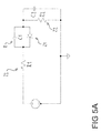
- FIG. 5A shows a schematic block circuit diagram of a circuit arrangement for simulation purposes
- FIG. 5B shows a schematic block circuit diagram of a circuit arrangement for simulation purposes
- FIGS. 6A and 6B show voltage-time graphs for a first set of parameters
- FIGS. 7A and 7B show voltage-time graphs for a second set of parameters
- FIGS. 8A and 8B show voltage-time graphs for a third set of parameters
- FIGS. 9A and 9B show voltage-time graphs for a fourth set of parameters
- FIGS. 10A and 10B show voltage-time graphs for a fifth set of parameters.
- FIGS. 11A and 11B show voltage-time graphs for a sixth set of parameters.
- Embodiments of the invention provide a circuit arrangement for actuating a first voltage-controlled semiconductor switching element and a bridge circuit and a power converter comprising such a circuit arrangement, which make it possible to reduce the duration for the provision of a matched switch-off voltage.
- Some embodiments provide a circuit arrangement for actuating a first voltage-controlled semiconductor switching element comprising a first electrode, a second electrode and a control electrode having a pulse generator, which is designed to generate an in particular unipolar control voltage input signal for actuating the first semiconductor switching element, wherein the control voltage input signals contain a switch-on voltage signal for switching on the first semiconductor switching element and a switch-off voltage signal for switching off the first semiconductor switching element.
- the circuit arrangement has a bias capacitor, whereas the bias capacitor is electrically connected or coupled to the pulse generator in such a way that an amplitude of a switch-off voltage signal which can be applied to the control electrode is variable by means of the bias capacitor.
- the circuit arrangement has a first electrical resistor.
- the first electrical resistor and the bias capacitor are connected electrically in series in an electrical path between a first connection of the pulse generator and a second connection of the pulse generator.
- the control electrode is electrically connected to a first connection of the bias capacitor and to a first connection of the first electrical resistor.
- the first electrode is electrically connected to a second connection of the pulse generator and to a second connection of the first electrical resistor.
- the circuit arrangement furthermore has a further capacitor, which is connected electrically in series with the first electrical resistor and the bias capacitor in the line path between the first connection of the pulse generator and the second connection of the pulse generator.
- a first connection of the pulse generator and a second connection of the pulse generator are understood here and below to mean that the first connection and the second connection are electrically connected or coupled to the pulse generator and therefore are electrically and operatively connected to the pulse generator without necessarily being connected to the pulse generator via a line path, however.
- the first electrical resistor will be understood here and below to mean a passive electrical component and not the physical quantity.
- the circuit arrangement in accordance with the mentioned embodiment enables a reduction in the duration for the provision of a varied or matched switch-off voltage.
- the amplitude of the switch-off voltage signal which can be applied to the control electrode can be varied by means of a superposition of the control voltage input signals with a charging voltage of the bias capacitor.
- the charging of the bias capacitor takes place when the circuit arrangement is switched on or when the component containing the circuit arrangement is switched on stepwise by virtue of the energy with which the control electrode is charged. This operation typically lasts a few milliseconds, during which the first semiconductor switching element can be switched off more slowly than a subsequent continuous operating mode.
- acceleration of the provision of the matched switch-off voltage is advantageously made possible.
- the charging of the bias capacitor is dependent on the energy which is output by the circuit arrangement to the control electrode of the first semiconductor switching element during each switch-on operation.
- the charging of the bias capacitor can be accelerated by virtue of the fact that an additional load is connected to the output of the circuit arrangement.
- this takes place by means of the first electrical resistor, which is arranged between the control electrode and the first electrode of the first semiconductor switching element. The costs for the entire circuit arrangement are in this case not significantly increased in an advantageous manner.
- the first electrical resistor and the bias capacitor are therefore arranged electrically in parallel with one another in a line path between the first electrode and the control electrode.
- the amplitude of the switch-off voltage signal which can be applied to the control electrode is variable by means of the bias capacitor in such a way that the switch-off voltage signal has a polarity which is opposite that of a switch-on voltage signal. As a result, a susceptibility to faults of the first semiconductor switching element can be reduced.
- the circuit arrangement furthermore has a first diode, wherein the first diode is connected electrically in series with the first electrical resistor and the bias capacitor in the electrical path between the first connection of the pulse generator and the second connection of the pulse generator.
- the first diode may be selected from the group consisting of a Schottky diode and a bipolar diode.
- the first electrical resistor and the first diode can be integrated monolithically in the circuit arrangement.
- the bias capacitor has a first capacitance C 1
- the capacitor has a third capacitance C 3 , wherein the first capacitance C 1 substantially corresponds to the third capacitance C 3 .
- C 1 C 3 .
- the further switching response of the circuit arrangement i.e. the switching response apart from the accelerated provision of the matched switched-off voltage
- the additional load in the form of the first electrical resistor not to subject the circuit arrangement to loading, as far as possible, after a transient phenomenon. This takes place by means of the provision of the capacitor and the first diode, which are connected in series with the first electrical resistor.
- the first electrical resistor loads the circuit arrangement thereby only as long as the capacitor is still not charged.
- the first semiconductor switching element can in particular be in the form of a MOSFET.
- the first electrode forms a source electrode
- the second electrode forms a drain electrode
- the control electrode forms a gate electrode of the MOSFET.
- the first semiconductor switching element can be in the form of a normally off n-channel MOSFET.
- the varied switch-off voltage signal in this configuration has a negative polarity
- the switch-on voltage signal has a positive polarity.
- the first semiconductor switching element can be in the form of an IGBT.
- the first electrode forms an emitter electrode
- the second electrode forms a collector electrode
- the control electrode forms a gate electrode of the IGBT.
- the circuit arrangement furthermore has a discharge circuit, which is designed to discharge the control electrode.
- the discharge circuit is in this case connected electrically in parallel with the bias capacitor, when viewed from the pulse generator, and has a second electrical resistor and a second semiconductor switching element.
- the second semiconductor switching element can in particular be in the form of a MOSFET or in the form of a bipolar transistor.
- the circuit arrangement furthermore has a second diode, wherein the second diode is connected electrically in parallel with the bias capacitor.
- the first electrical resistor is connected electrically in series with the parallel circuit comprising the second diode and the bias capacitor in the electrical path between the first connection of the pulse generator and the second connection of the pulse generator.
- a maximum charging voltage for the bias capacitor can be set by means of the second diode.
- the second diode may be in the form of a Zener diode for this purpose.
- the first electrical resistor has a resistance of 100 ohms. It is thus possible to ensure that the first electrical resistor does not short-circuit the circuit arrangement even during a transient phenomenon.
- bridge circuit which has a circuit arrangement in accordance with one of the mentioned embodiments.
- the bridge circuit can be in the form of a half-bridge circuit.
- the bridge circuit and the power converter in accordance with the application have the advantages which have already been mentioned in connection with the circuit arrangement according to the application and which will not be set forth again at this juncture so as to avoid repetition.
- FIG. 1A shows a block circuit diagram of a circuit arrangement 1 for actuating voltage-controlled semiconductor switching elements 2 and 2 ′.
- the semiconductor switching elements 2 and 2 ′ are in the form of normally off n-channel MOSFETs and each have a first electrode 3 in the form of a source electrode, a second electrode 4 in the form of a drain electrode, and a control electrode 5 in the form of a gate electrode.
- the circuit arrangement 1 therefore forms a gate driver circuit in the embodiment shown, and the first electrode 3 forms a reference electrode for the control electrode 5 .
- the semiconductor switching elements 2 and 2 ′ are part of a half-bridge circuit, wherein the semiconductor switching elements 2 form a so-called high-side switch, and the semiconductor switching elements 2 ′ form a so-called low-side switch of the half-bridge circuit.
- the circuit arrangement 1 has a first pulse generator and a second pulse generator.
- the first pulse generator comprises a first amplifier 6 and a transformer 24 having a primary side 25 and a secondary side 26 , wherein the first amplifier 6 is electrically connected to the primary side 25 of the transformer 24 .
- the second pulse generator comprises a second amplifier 6 ′ and a transformer 24 having a primary side 25 and a secondary side 26 , wherein the second amplifier 6 is electrically connected to the primary side 25 of the transformer 24 .
- the first and second pulse generators have a common transformer 24 .
- the transformer 24 has a common input coil on the primary side 25 , which common input coil is connected between the first and second amplifiers 6 , 6 ′.
- the transformer 24 has in each case one output coil, each having a first electrical connection 10 and a second electrical connection 11 .
- the first pulse generator is designed to generate unipolar control voltage input signals 7
- the second pulse generator is designed to generate unipolar control voltage input signals 7 ′.
- the control voltage input signals 7 and 7 ′ each have a switch-on voltage signal for switching on the semiconductor switching element 2 and 2 ′, respectively, and a switch-off voltage signal for switching off the semiconductor switching element 2 and 2 ′, respectively, wherein the control voltage input signals 7 and 7 ′ are phase-shifted through 180° with respect to one another in relation to the pulse/no-pulse ratio.
- the switch-off voltage signal which can be applied to the respective control electrode 5 it is effected that no electrically conductive channel is formed in the semiconductor switching element 2 or 2 ′, whereas, by means of the switch-on voltage signal, a control voltage is applied to the control electrode 5 , in which an electrically conductive channel is formed. Further details in respect of the actuation of the semiconductor switching elements 2 and 2 ′ will be explained in more detail below.
- the circuit arrangement 1 has in each case one bias capacitor 8 for the semiconductor switching elements 2 and 2 ′.
- the bias capacitors 8 are in this case electrically connected to the respective pulse generator via the respective first connection 10 and the respective second connection 11 in such a way that an amplitude of a switch-off voltage signal which can be applied to the control electrode 5 of the corresponding semiconductor switching element 2 or 2 ′ is variable by means of the respective bias capacitor 8 .
- the amplitude is variable in such a way that a negative switch-off voltage signal can be provided which therefore has the opposite polarity to that of a positive switch-on voltage signal.
- the circuit arrangement 1 has, on the secondary side of the transformer 24 , in each case one first electrical resistor 9 for the semiconductor switching elements 2 and 2 ′.
- the circuit arrangement 1 has in each case one second diode 21 for the semiconductor switching elements 2 and 2 ′, wherein the second diode 21 is connected electrically in parallel with the respective bias capacitor 8 . Therefore, in the embodiment shown, the first electrical resistor 9 is connected electrically in series with the parallel circuit comprising the second diode 21 and the bias capacitor 8 in an electrical path between the first connection 10 and the second connection 11 of the corresponding pulse generator.
- the second diode 21 is in the form of a Zener diode, for example.
- the maximum charging voltage of the bias capacitor 8 can be set by means of the second diode 21 .
- the control electrode 5 of the respective semiconductor switching element 2 or 2 ′ is electrically connected to a first connection 12 of the corresponding bias capacitor 8 and to a first connection 13 of the corresponding first electrical resistor 9 .
- the first electrode 3 of the respective semiconductor switching element 2 or 2 ′ is electrically connected to a second connection 14 of the corresponding bias capacitor 8 and to a second connection 15 of the corresponding first electrical resistor 9 .
- the first electrical resistor 9 and the parallel circuit comprising the second diode 21 and the bias capacitor 8 are arranged electrically in parallel with one another in a line path between the first electrode 3 and the control electrode 5 and are electrically connected to the first electrode 3 and the control electrode 5 .
- the circuit arrangement 1 furthermore has a first diode 16 and a capacitor 17 , wherein the first diode 16 and the capacitor 17 are connected electrically in series with the first electrical resistor 9 and the parallel circuit comprising the second diode 21 and the bias capacitor 8 in the electrical path between the first connection 10 and the second connection 11 of the corresponding pulse generator.
- the first diode 16 is, for example, selected from the group consisting of a Schottky diode and a bipolar diode
- the bias capacitor 8 typically has a first capacitance C 1 , which substantially corresponds to a third capacitance C 3 of the capacitor 17 .
- the relationship C 1 C 3 can apply.
- the first connection 12 of the bias capacitor 8 is electrically connected to the first diode 16
- the first diode 16 is furthermore electrically connected to the first connection 13 of the first electrical resistor 9
- the second connection 15 of the first electrical resistor 9 is in addition electrically connected to the capacitor 17 .
- the control voltage input signals 7 and 7 ′ for actuating the semiconductor switching elements 2 and 2 ′, respectively, are transmitted to the semiconductor switching elements 2 and 2 ′ by means of the transformer 24 .
- the discharge of the respective gate electrode takes place on the secondary side 26 of the transformer by means of a discharge circuit 18 , wherein the discharge circuit 18 is connected electrically in parallel with the series circuit comprising the respective bias capacitor 8 and the respective control electrode 5 and has a second electrical resistor 19 and a second semiconductor switching element 20 , wherein the second semiconductor switching element 20 forms a switch-off MOSFET in the embodiment shown.
- the charging voltage of the corresponding bias capacitor 8 is superposed on the respective gate signal.
- the charging of the bias capacitor 8 during switch-on in this case takes place stepwise owing to the energy with which the respective MOSFET gate is charged.
- the provision of the negative switch-off voltage can be accelerated without the other switching response of the circuit arrangement 1 being changed. Since the charging of the bias capacitors 8 is dependent on the energy which is emitted by the gate driver during each switch-on operation to the respective gate of the semiconductor switching elements 2 and 2 ′, this can be accelerated by virtue of the fact that an additional load is connected to the output of the gate driver.
- the first electrical resistor 9 which has a relatively low resistance between the respective gate and source connections of the two MOSFETs.
- the first electrical resistor 9 is in this case dimensioned in such a way that it does not short-circuit the circuit arrangement 1 even during the transient condition and is typically 100 ohms.
- the capacitor 17 and the first diode 16 are connected in series with the first electrical resistor 9 .
- the first electrical resistor 9 thus loads the circuit arrangement 1 only as long as the capacitor 17 is not yet charged.
- the circuit arrangement 1 in the embodiment shown has a second electrical resistor 22 , which is connected electrically in parallel with the capacitor 17 and is used for discharging the capacitor 17 .
- the circuit arrangement 1 has a third electrical resistor 23 , which is connected electrically in series with the parallel circuit comprising the second diode 21 and the bias capacitor 8 and forms a charging resistor for the bias capacitor 8 .
- FIG. 1B shows a block circuit diagram of a circuit arrangement in accordance with a second embodiment of the application.
- Components having the same functions as in FIG. 1A are identified by the same reference symbols and will not be explained again below.
- the second embodiment shown in FIG. 1B differs from the first embodiment shown in FIG. 1A to the extent that the order of the arrangement of the first electrical resistor 9 and the first diode 16 in the electrical path between the first connection 10 and the second connection 11 is swapped over, i.e. the first connection 12 of the bias capacitor 8 is electrically connected to the first connection 13 of the first electrical resistor 9 , and the second connection 15 of the first electrical resistor 9 is electrically connected to the first diode 16 .
- the first diode 16 is connected to the capacitor 17 .
- the order of the arrangement of the first electrical resistor 9 , the first diode 16 and the capacitor 17 in the electrical series circuit formed by these components can be switched as desired, wherein the second electrical resistor 22 is always connected electrically in parallel with the capacitor 17 .
- FIG. 2 shows a block circuit diagram of a circuit arrangement 1 in accordance with a third embodiment of the application.
- Components with the same functions as in the previous figures are identified by the same reference symbols and will not be explained again below.
- the third embodiment shown in FIG. 2 differs from the previous embodiments in that only one pulse generator is arranged on the primary side 25 of the transformer 24 , wherein again an amplifier 6 of the pulse generator is illustrated. Thus, the voltage amplitude is halved in comparison with the previous embodiments. Correspondingly, only control voltage input signals 7 for actuating the semiconductor switching elements 2 and 2 ′ are generated by means of the pulse generator.
- FIG. 3A shows a block circuit diagram of a circuit arrangement 1 in accordance with a fourth embodiment of the application.
- the embodiment shown in FIG. 3A differs from the previous embodiments in that the circuit arrangement 1 has only one semiconductor switching element 2 in the form of a normally off n-channel MOSFET.
- the embodiment shown does not have a transformer. The pulse generator is therefore not galvanically isolated from the further components.
- the embodiment shown in FIG. 3A does not contain any further capacitor in addition to the bias capacitor 8 and does not contain a second electrical resistor arranged in parallel with said further capacitor or a discharge circuit in accordance with the previous embodiments.
- FIG. 3B shows a block circuit diagram of a circuit arrangement in accordance with a fifth embodiment of the application.
- Components having the same functions as in the previous figures are identified by the same reference symbols and will not be explained again below.
- the embodiment shown in FIG. 3B differs from the embodiment shown in FIG. 3A in that the circuit arrangement 1 has a capacitor 17 in addition to the bias capacitor 8 , wherein the capacitor 17 is connected electrically in series with the first electrical resistor 9 and the parallel circuit comprising the second diode 21 and the bias capacitor 8 in the line path between the first connection 10 of the pulse generator and the second connection 11 of the pulse generator.
- the circuit arrangement 1 has a second electrical resistor 22 , which is connected electrically in parallel with the capacitor 17 .
- FIG. 4 shows a block circuit diagram of a circuit arrangement 1 in accordance with a sixth embodiment of the application.
- Components with the same functions as in the previous figures are identified by the same reference symbols and will not be explained again below.
- the embodiment shown in FIG. 4 differs from the embodiment shown in FIG. 2 in that the discharge circuit 18 has a second semiconductor switching element 20 in the form of a bipolar transistor.
- the embodiments of the circuit arrangement 1 shown in FIGS. 1A to 4 merely represent exemplary gate driver circuits.
- the acceleration circuit in accordance with the application can in this case be used in any gate driver which has a bias capacitor 8 which is charged by the gate energy.
- Such gate drivers are used, for example, in DC-to-DC converters of the medium power class, i.e. from several hundred watts to several kilowatts.
- the circuit arrangement 1 can be used for DC-to-DC converters which are used in solar installations.
- FIG. 5A shows a schematic block circuit diagram of a circuit arrangement which forms the basis for the simulations shown in FIGS. 6A and 6B
- FIG. 5B shows a schematic block circuit diagram of a circuit arrangement which forms the basis for the simulations shown in FIGS. 7A to 11B .
- Components with the same functions as in the previous figures are identified by the same reference symbols and will not be explained again below.
- FIG. 5A in this case shows a schematic block circuit diagram of a circuit arrangement which does not have an acceleration circuit in accordance with the application
- FIG. 5B shows a circuit arrangement in accordance with the application.
- the pulse generator is illustrated merely schematically as voltage source in FIGS. 5A and 5B .
- the semiconductor switching element in the form of a MOSFET to be actuated is not illustrated in any more detail in FIGS. 5A and 5B .
- the pulse generator generates unipolar square-wave control voltage input signals, which are between zero volts and 18 V, wherein the rising and falling edges each have a rise and fall time, respectively, of 100 ns.
- the pulse duration is 4.9 ⁇ s and the period is 10 ⁇ s, i.e. the interval between the pulses is 4.9 ⁇ s, taking into consideration the rise and fall times.
- FIGS. 6A and 6B show voltage-time graphs for the first set of parameters.
- FIG. 6A shows an overview of the characteristic of the voltage over time in a time interval of 2 ms
- FIG. 6B shows a detail view of a time interval of 200 ⁇ s, wherein the control voltage input signals generated by the pulse generator are illustrated in the respective upper voltage-time graph, and the voltage applied to the control electrode in the form of the gate electrode is illustrated in the respective lower voltage-time graph.
- FIGS. 7A and 7B show voltage-time graphs for the second set of parameters, which in this case contains optimally selected parameters.
- FIG. 7A shows an overview of the characteristic of the voltage over time in a time interval of 2 ms
- FIG. 7B shows a detail view of a time interval of 200 ⁇ s, wherein the voltage of the capacitor is illustrated in the respective upper voltage-time graph, the control voltage input signals generated by the pulse generator are illustrated in the respective central voltage-time graph, and the voltage applied to the control electrode in the form of the gate electrode is illustrated in the respective lower voltage-time graph.
- the negative amplitude of a switch-off voltage signal which can be applied to the control electrode can be varied from 0 V to ⁇ 2 V by virtue of the provision of the bias capacitor 8 and therefore a negative switch-off voltage can be provided.
- the duration of the provision of the negative switch-off voltage can in this case be advantageously shortened in comparison with the duration of the circuit arrangement shown in FIG. 5A by the provision of the first electrical resistor 9 .
- FIGS. 8A to 11B show voltage-time graphs for the further sets of parameters, wherein again an overview of the characteristic of the voltage over time in a time interval of 2 ms and a detail view of the time interval of 200 ⁇ s are shown.
- the duration for the provision of the negative switch-off voltage can be reduced if the resistance of the resistor and/or the capacitance are reduced.
Landscapes
- Engineering & Computer Science (AREA)
- Power Engineering (AREA)
- Electronic Switches (AREA)
- Power Conversion In General (AREA)
- Generation Of Surge Voltage And Current (AREA)
Applications Claiming Priority (4)
| Application Number | Priority Date | Filing Date | Title |
|---|---|---|---|
| DE102012207155 | 2012-04-30 | ||
| DE102012207155.5 | 2012-04-30 | ||
| DE201210207155 DE102012207155B4 (de) | 2012-04-30 | 2012-04-30 | Schaltungsanordnung zum Ansteuern eines Halbleiter-Schaltelements |
| PCT/EP2013/058371 WO2013164222A1 (de) | 2012-04-30 | 2013-04-23 | Schaltungsanordnung zum ansteuern eines halbleiter-schaltelements |
Publications (2)
| Publication Number | Publication Date |
|---|---|
| US20150124507A1 US20150124507A1 (en) | 2015-05-07 |
| US9496862B2 true US9496862B2 (en) | 2016-11-15 |
Family
ID=48170483
Family Applications (1)
| Application Number | Title | Priority Date | Filing Date |
|---|---|---|---|
| US14/397,732 Active 2033-10-28 US9496862B2 (en) | 2012-04-30 | 2013-04-23 | Circuit arrangement for actuating a semiconductor switching element |
Country Status (4)
| Country | Link |
|---|---|
| US (1) | US9496862B2 (de) |
| CN (1) | CN104620504B (de) |
| DE (1) | DE102012207155B4 (de) |
| WO (1) | WO2013164222A1 (de) |
Cited By (2)
| Publication number | Priority date | Publication date | Assignee | Title |
|---|---|---|---|---|
| US9966837B1 (en) | 2016-07-08 | 2018-05-08 | Vpt, Inc. | Power converter with circuits for providing gate driving |
| US10680527B2 (en) * | 2018-05-30 | 2020-06-09 | Yokogawa Electric Corporation | Pulse signal output circuit |
Families Citing this family (10)
| Publication number | Priority date | Publication date | Assignee | Title |
|---|---|---|---|---|
| DE102012207155B4 (de) | 2012-04-30 | 2013-11-21 | Conti Temic Microelectronic Gmbh | Schaltungsanordnung zum Ansteuern eines Halbleiter-Schaltelements |
| WO2015016891A1 (en) * | 2013-07-31 | 2015-02-05 | Schneider Electric Solar Inverters Usa, Inc. | Isolated uni-polar transistor gate drive |
| CN104716816A (zh) * | 2013-12-17 | 2015-06-17 | 台达电子企业管理(上海)有限公司 | 功率转换装置、隔离驱动电路与隔离驱动方法 |
| US9461642B1 (en) * | 2015-08-26 | 2016-10-04 | Southwest Research Institute | Radiation-tolerant high-speed high-voltage pulser |
| JP6745660B2 (ja) * | 2016-07-08 | 2020-08-26 | ローム株式会社 | ゲート駆動回路 |
| KR101806731B1 (ko) * | 2016-08-17 | 2017-12-08 | 현대자동차주식회사 | 게이트 구동 장치 |
| US10211828B2 (en) * | 2016-09-08 | 2019-02-19 | Panasonic Intellectual Property Management Co., Ltd. | Driving device for insulated gate semiconductor element, and driving system for the same element |
| JP6985600B2 (ja) * | 2018-01-25 | 2021-12-22 | 富士通株式会社 | 波形成形回路、半導体装置及びスイッチング電源装置 |
| CN110868073B (zh) * | 2019-08-26 | 2021-04-13 | 哈尔滨工业大学 | 一种基于多绕组变压器耦合的串联SiC MOSFET驱动电路 |
| DE102021214521A1 (de) | 2021-12-16 | 2023-06-22 | Robert Bosch Gesellschaft mit beschränkter Haftung | Vorrichtung, Halbbrücke und Verfahren zum Betreiben einer Vorrichtung |
Citations (11)
| Publication number | Priority date | Publication date | Assignee | Title |
|---|---|---|---|---|
| US4052623A (en) | 1976-08-10 | 1977-10-04 | General Electric Company | Isolated semiconductor gate control circuit |
| DE4441492A1 (de) | 1994-11-22 | 1996-05-23 | Abb Research Ltd | Potentialtrennende Treiberschaltung zur Ansteuerung spannungsgesteuerter Halbleiterventile |
| US5763962A (en) * | 1995-09-22 | 1998-06-09 | Ecg Co., Ltd. | Semiconductor switch driving circuit |
| US5786687A (en) * | 1996-12-03 | 1998-07-28 | Compaq Computer Corporation | Transformer-isolated pulse drive circuit |
| US6016259A (en) | 1996-12-24 | 2000-01-18 | Matsushita Electric Works, Ltd. | Power supply circuit |
| US6094087A (en) * | 1997-07-30 | 2000-07-25 | Lucent Technologies Inc. | Gate drive circuit for isolated gate devices and method of operation thereof |
| DE102005029353A1 (de) | 2005-06-22 | 2006-12-28 | Iav Gmbh Ingenieurgesellschaft Auto Und Verkehr | Steuerschaltung für spannungsgesteuerte Halbleiterschalter vorzugsweise in Halbbbrückenkonfiguration |
| JP2010130786A (ja) | 2008-11-27 | 2010-06-10 | Denso Corp | パワースイッチング素子の駆動回路 |
| US20110285447A1 (en) * | 2010-05-19 | 2011-11-24 | Sanken Electric Co., Ltd. | Drive circuit |
| US20120008344A1 (en) * | 2010-07-07 | 2012-01-12 | Jian-Hong Zeng | Driver for driving power switch element |
| WO2013164222A1 (de) | 2012-04-30 | 2013-11-07 | Conti Temic Microelectronic Gmbh | Schaltungsanordnung zum ansteuern eines halbleiter-schaltelements |
Family Cites Families (3)
| Publication number | Priority date | Publication date | Assignee | Title |
|---|---|---|---|---|
| JP4640495B2 (ja) * | 2008-11-27 | 2011-03-02 | トヨタ自動車株式会社 | 電気絶縁型スイッチング素子駆動装置 |
| JP4787350B2 (ja) * | 2009-10-14 | 2011-10-05 | Smk株式会社 | 自励式スイッチング電源回路 |
| CN201781466U (zh) * | 2010-09-07 | 2011-03-30 | 中国电子科技集团公司第十四研究所 | 单脉冲变压器沿触发小型浮动板调制器 |
-
2012
- 2012-04-30 DE DE201210207155 patent/DE102012207155B4/de active Active
-
2013
- 2013-04-23 CN CN201380022790.7A patent/CN104620504B/zh active Active
- 2013-04-23 WO PCT/EP2013/058371 patent/WO2013164222A1/de active Application Filing
- 2013-04-23 US US14/397,732 patent/US9496862B2/en active Active
Patent Citations (12)
| Publication number | Priority date | Publication date | Assignee | Title |
|---|---|---|---|---|
| US4052623A (en) | 1976-08-10 | 1977-10-04 | General Electric Company | Isolated semiconductor gate control circuit |
| DE4441492A1 (de) | 1994-11-22 | 1996-05-23 | Abb Research Ltd | Potentialtrennende Treiberschaltung zur Ansteuerung spannungsgesteuerter Halbleiterventile |
| US5763962A (en) * | 1995-09-22 | 1998-06-09 | Ecg Co., Ltd. | Semiconductor switch driving circuit |
| US5786687A (en) * | 1996-12-03 | 1998-07-28 | Compaq Computer Corporation | Transformer-isolated pulse drive circuit |
| US6016259A (en) | 1996-12-24 | 2000-01-18 | Matsushita Electric Works, Ltd. | Power supply circuit |
| DE69720176T2 (de) | 1996-12-24 | 2003-10-23 | Matsushita Electric Works Ltd | Stromversorgungsschaltung |
| US6094087A (en) * | 1997-07-30 | 2000-07-25 | Lucent Technologies Inc. | Gate drive circuit for isolated gate devices and method of operation thereof |
| DE102005029353A1 (de) | 2005-06-22 | 2006-12-28 | Iav Gmbh Ingenieurgesellschaft Auto Und Verkehr | Steuerschaltung für spannungsgesteuerte Halbleiterschalter vorzugsweise in Halbbbrückenkonfiguration |
| JP2010130786A (ja) | 2008-11-27 | 2010-06-10 | Denso Corp | パワースイッチング素子の駆動回路 |
| US20110285447A1 (en) * | 2010-05-19 | 2011-11-24 | Sanken Electric Co., Ltd. | Drive circuit |
| US20120008344A1 (en) * | 2010-07-07 | 2012-01-12 | Jian-Hong Zeng | Driver for driving power switch element |
| WO2013164222A1 (de) | 2012-04-30 | 2013-11-07 | Conti Temic Microelectronic Gmbh | Schaltungsanordnung zum ansteuern eines halbleiter-schaltelements |
Non-Patent Citations (1)
| Title |
|---|
| International Search Report and Written Opinion, Application No. PCT/EP2013/058371, 19 pages, Oct. 10, 2013. |
Cited By (2)
| Publication number | Priority date | Publication date | Assignee | Title |
|---|---|---|---|---|
| US9966837B1 (en) | 2016-07-08 | 2018-05-08 | Vpt, Inc. | Power converter with circuits for providing gate driving |
| US10680527B2 (en) * | 2018-05-30 | 2020-06-09 | Yokogawa Electric Corporation | Pulse signal output circuit |
Also Published As
| Publication number | Publication date |
|---|---|
| WO2013164222A1 (de) | 2013-11-07 |
| CN104620504A (zh) | 2015-05-13 |
| CN104620504B (zh) | 2018-06-12 |
| US20150124507A1 (en) | 2015-05-07 |
| DE102012207155A1 (de) | 2013-10-31 |
| DE102012207155B4 (de) | 2013-11-21 |
Similar Documents
| Publication | Publication Date | Title |
|---|---|---|
| US9496862B2 (en) | Circuit arrangement for actuating a semiconductor switching element | |
| US9397658B2 (en) | Gate drive circuit and a method for controlling a power transistor | |
| JP6402591B2 (ja) | 半導体装置 | |
| US20230275397A1 (en) | Pulsed laser diode driver | |
| US9729060B2 (en) | Power conversion apparatus having DC-DC converters with different gate resistances | |
| US9923557B2 (en) | Switching circuit and power conversion circuit | |
| CN113098469A (zh) | 用于GaN开关的时间可编程失效安全下拉电路 | |
| US10020731B2 (en) | Power switch circuit | |
| JP2009515501A (ja) | 半導体スイッチをガルバニック絶縁で制御する方法および回路装置 | |
| JP2007336694A (ja) | 絶縁ゲート型半導体素子の駆動回路 | |
| US20080197904A1 (en) | Circuit Arrangement for Switching a Load | |
| US9344006B2 (en) | Driving circuit for a transistor | |
| US7355351B2 (en) | Circuit arrangement having a converter without a transformer but with an inductor for the pulsed operation of dielectric barrier discharge lamps | |
| EP2890009A1 (de) | Spannungsregler und resonanter Gattertreiber dafür | |
| JP5761656B2 (ja) | ゲートドライブ回路 | |
| JP5254386B2 (ja) | ゲート駆動回路、およびパワー半導体モジュール | |
| JP5407618B2 (ja) | ゲート駆動回路及び電力変換回路 | |
| JP6295268B2 (ja) | 半導体駆動装置 | |
| JP2014150654A (ja) | ゲート駆動回路 | |
| KR20160071842A (ko) | 게이트 구동부 및 그의 구동방법 | |
| JP5563050B2 (ja) | ゲート駆動回路、およびパワー半導体モジュール | |
| US9660510B2 (en) | Voltage converter for a motor vehicle | |
| US10560018B2 (en) | Modulated power supply | |
| JP2004088892A (ja) | 絶縁ゲート型半導体素子のゲート回路 | |
| US11863077B2 (en) | Power supply system with active clamping |
Legal Events
| Date | Code | Title | Description |
|---|---|---|---|
| AS | Assignment |
Owner name: CONTI TEMIC MICROELECTRONIC GMBH, GERMANY Free format text: ASSIGNMENT OF ASSIGNORS INTEREST;ASSIGNOR:RIDDER, MATTHIAS;REEL/FRAME:037207/0624 Effective date: 20151122 |
|
| AS | Assignment |
Owner name: CONTI TEMIC MICROELECTRONIC GMBH, GERMANY Free format text: ASSIGNMENT OF ASSIGNORS INTEREST;ASSIGNOR:RIDDER, MATTHIAS;REEL/FRAME:038364/0907 Effective date: 20151122 |
|
| STCF | Information on status: patent grant |
Free format text: PATENTED CASE |
|
| FEPP | Fee payment procedure |
Free format text: PAYOR NUMBER ASSIGNED (ORIGINAL EVENT CODE: ASPN); ENTITY STATUS OF PATENT OWNER: LARGE ENTITY |
|
| MAFP | Maintenance fee payment |
Free format text: PAYMENT OF MAINTENANCE FEE, 4TH YEAR, LARGE ENTITY (ORIGINAL EVENT CODE: M1551); ENTITY STATUS OF PATENT OWNER: LARGE ENTITY Year of fee payment: 4 |
|
| AS | Assignment |
Owner name: VITESCO TECHNOLOGIES GERMANY GMBH, GERMANY Free format text: ASSIGNMENT OF ASSIGNORS INTEREST;ASSIGNOR:CONTI TEMIC MICROELECTRONIC GMBH;REEL/FRAME:053107/0097 Effective date: 20200610 |
|
| MAFP | Maintenance fee payment |
Free format text: PAYMENT OF MAINTENANCE FEE, 8TH YEAR, LARGE ENTITY (ORIGINAL EVENT CODE: M1552); ENTITY STATUS OF PATENT OWNER: LARGE ENTITY Year of fee payment: 8 |