US9335371B2 - Semiconductor evaluating device and semiconductor evaluating method - Google Patents
Semiconductor evaluating device and semiconductor evaluating method Download PDFInfo
- Publication number
- US9335371B2 US9335371B2 US14/065,064 US201314065064A US9335371B2 US 9335371 B2 US9335371 B2 US 9335371B2 US 201314065064 A US201314065064 A US 201314065064A US 9335371 B2 US9335371 B2 US 9335371B2
- Authority
- US
- United States
- Prior art keywords
- fluid
- measuring object
- semiconductor
- evaluating device
- semiconductor device
- Prior art date
- Legal status (The legal status is an assumption and is not a legal conclusion. Google has not performed a legal analysis and makes no representation as to the accuracy of the status listed.)
- Active, expires
Links
Images


Classifications
-
- G—PHYSICS
- G01—MEASURING; TESTING
- G01R—MEASURING ELECTRIC VARIABLES; MEASURING MAGNETIC VARIABLES
- G01R31/00—Arrangements for testing electric properties; Arrangements for locating electric faults; Arrangements for electrical testing characterised by what is being tested not provided for elsewhere
- G01R31/28—Testing of electronic circuits, e.g. by signal tracer
- G01R31/2851—Testing of integrated circuits [IC]
- G01R31/2886—Features relating to contacting the IC under test, e.g. probe heads; chucks
Definitions
- the present invention relates to a semiconductor evaluating device and a semiconductor evaluating method which execute evaluation for an electrical characteristic of a measuring object in a state in which a fluid is sprayed onto the measuring object.
- a surface where the measuring object is to be provided is fixed by vacuum adsorption or the like in a state where the surface thereof is in contact with a surface of a chuck stage, and a contact prober is then caused to come in contact with a front surface of the measuring object in order to carry out electrical input/output.
- the number of pins in the contact probe has been increased by a request for applying a large current or a high voltage, or the like.
- the Japanese Patent Application Laid-Open No. 2003-130889 describes the technique for inspecting the characteristic of an electronic component in an insulating liquid, thereby preventing a discharge from occurring during the characteristic inspection.
- the Japanese Patent Application Laid-Open No. 10-96746 (1998) describes the technique for executing the characteristic inspection for a thing to be inspected in a closed space filled with an inert gas without using the insulating liquid, thereby preventing the discharge from occurring during the characteristic inspection.
- the technique described in the Japanese Patent Application Laid-Open No. 2003-130889 has a problem in that an expensive prober is necessary, and furthermore, a time required for the evaluating step is increased and a cost cannot be reduced because of the evaluation in the liquid.
- the measuring object is a semiconductor element in a wafer test and a chip test
- a semiconductor evaluating device includes a chuck stage for holding a measuring object, a contact probe for evaluating an electrical characteristic of the measuring object held on the chuck stage in contact with the measuring object, and a fluid spraying portion for spraying a fluid onto the measuring object.
- the semiconductor evaluating device includes the chuck stage for holding a measuring object, the contact probe for evaluating an electrical characteristic of the measuring object held on the chuck stage in contact with the measuring object, and the fluid spraying portion for spraying a fluid onto the measuring object.
- the fluid is sprayed onto the measuring object by the fluid spraying portion. Consequently, it is possible to easily prevent the partial discharge from occurring in the evaluation.
- the fluid is sprayed onto the measuring object. For this reason, it is not necessary to tightly seal a measurement space in which the contact probe and the measuring object are disposed. Moreover, there is not required additional processing for filling with the fluid every evaluation or removing the fluid from the measuring object after the evaluation. Therefore, it is possible to reduce a cost and to prevent a time required for an evaluating process from being increased.
- a semiconductor evaluating method includes the steps of electrically evaluating the measuring object by causing the contact probe to come in contact with the measuring object, and spraying a fluid onto a front surface of the measuring object by the fluid spraying portion in the step of electrically evaluating the measuring object.
- the semiconductor evaluating method includes the steps of electrically evaluating the measuring object by causing the contact probe to come in contact with the measuring object, and spraying a fluid onto a front surface of the measuring object by the fluid spraying portion in the step of electrically evaluating the measuring object.
- the fluid is sprayed onto the measuring object by the fluid spraying portion. Consequently, it is possible to easily prevent the partial discharge from occurring in the evaluation.
- FIG. 1 is a schematic view showing a semiconductor evaluating device according to a first preferred embodiment
- FIG. 2 is a view for explaining an operation of a contact probe in the semiconductor evaluating device according to the first preferred embodiment
- FIG. 3 is a plan view showing a structure in which a fluid spraying portion and a fluid sucking portion are disposed in the semiconductor evaluating device according to the first preferred embodiment
- FIG. 4 is a plan view showing a structure in which a fluid spraying portion and a fluid sucking portion are disposed in a semiconductor evaluating device according to a first variant of the first preferred embodiment
- FIG. 5 is a front view showing a structure in which a fluid spraying portion is disposed in a semiconductor evaluating device according to a second variant of the first preferred embodiment
- FIG. 6 is a front view showing a structure in which a fluid spraying portion is disposed in a semiconductor evaluating device according to a third variant of the first preferred embodiment
- FIG. 7 is a plan view showing a structure in which a fluid spraying portion and a fluid sucking portion are disposed in a semiconductor evaluating device according to a fourth variant of the first preferred embodiment
- FIG. 8 is a plan view showing a structure in which a fluid spraying portion and a fluid sucking portion are disposed in a semiconductor evaluating device according to a fifth variant of the first preferred embodiment
- FIG. 9 is a schematic view showing a semiconductor evaluating device according to a second preferred embodiment.
- FIG. 10 is a schematic view showing a semiconductor evaluating device according to a third preferred embodiment.
- FIG. 11 is a plan view showing a structure in which a fluid spraying portion is disposed in the semiconductor evaluating device according to the third preferred embodiment
- FIG. 12 is a view for explaining an operation of a contact probe in the semiconductor evaluating device according to the third preferred embodiment.
- FIG. 13 is a plan view showing a structure in which a fluid spraying portion is disposed in a semiconductor evaluating device according to a first variant of the third preferred embodiment.
- FIG. 1 is a schematic view showing a semiconductor evaluating device 1 according to the first preferred embodiment.
- the semiconductor evaluating device 1 includes a probe substrate 2 , a chuck stage 3 , a control unit 4 , a fluid spraying portion 7 , a fluid sucking portion 17 , and a moving arm 9 .
- the probe substrate 2 includes a contact probe 10 , an insulating substrate 16 and a connecting portion 8 b .
- the fluid spraying portion 7 and the fluid sucking portion 17 are provided on the insulating substrate 16 , and an electrical characteristic of a semiconductor device 5 is evaluated in a state in which a fluid is sprayed onto a surface of the semiconductor device 5 .
- the semiconductor device 5 having a longitudinal structure for causing a large current to flow in a longitudinal direction of the semiconductor device 5 that is, an out-of-plane direction
- the present invention is not restricted thereto but it is also possible to employ a semiconductor device having a horizontal structure which carries out input/output in one of surfaces of the semiconductor device.
- one of electrodes for connection to an outside is the contact probe 10 which comes in contact with a connecting pad 18 (see FIG. 2 ) provided on an upper surface of the semiconductor device 5 .
- the other electrode is a lower surface of the semiconductor device 5 , that is, an upper surface of the chuck stage 3 to come in contact at an installation surface.
- the contact probe 10 is fixed to the insulating substrate 16 and is connected to the control unit 4 through a signal line 6 b connected to the connecting portion 8 b of the insulating substrate 16 .
- the chuck stage 3 is connected to the control unit 4 through a signal line 6 a connected to a connecting portion 8 a provided on a side surface of the chuck stage 3 .
- the plurality of contact probes 10 are provided on the assumption that a large current is applied. It is desirable that the respective connecting portions 8 a and 8 b should be provided in positions in which a distance from each of the contact probes 10 to the connecting portion 8 b to be a connecting position for the signal line 6 b and the insulating substrate 16 and a distance from each of the contact probes 10 to the connecting portion 8 a provided on the side surface of the chuck stage 3 are almost coincident with each other through any of the contact probes 10 in such a manner that current densities to be applied to the respective contact probes 10 are almost equal to each other. In other words, it is desirable that the connecting portion 8 a and the connecting portion 8 b should be placed in opposed positions to each other through the contact probe 10 . Moreover, each of the contact probes 10 and the connecting portion 8 b are connected to each other through a metal plate (not shown) which is provided on the insulating substrate 16 , for example.
- the probe substrate 2 is held movably in an optional direction by means of the moving arm 9 .
- the moving arm 9 may have a structure in which the chuck stage 3 is held movably to move the semiconductor device 5 , that is, the chuck stage 3 side in place of the probe substrate 2 .
- the chuck stage 3 is a seat for fixing (holding) the semiconductor device 5 in contact with an installation surface of the semiconductor device 5 , and has a function of vacuum adsorption as means for fixing the semiconductor device 5 , for example.
- the means for fixing the semiconductor device 5 is not restricted to the vacuum adsorption but may be electrostatic adsorption or the like.
- FIG. 2 is a view for explaining an operation of the contact probe 10 in the semiconductor evaluating device 1 according to the first preferred embodiment, and part (a) of FIG. 2 shows an initial state, part (b) of FIG. 2 shows a contact state and part (c) of FIG. 2 shows a pressing state.
- the contact probe 10 is formed as a base and is fixed to the insulating substrate 16 in a downward direction (in a ⁇ Z direction).
- the contact probe 10 includes an installing portion 14 to be fixed to the insulating substrate 16 , a tip portion 12 having a contact portion 11 to mechanically and electrically come in contact with the connecting pad 18 provided on the upper surface of the semiconductor device 5 , a push-in portion 13 which is slidable in contact through a spring member such as a spring incorporated into an inner part, and an electrical connecting portion 15 which is electrically conducted to the tip portion 12 and serves as an output terminal to an outside.
- the contact probe 10 is formed by a metallic material such as copper, tungsten or rhenium tungsten which has an electrical conductivity
- the present invention is not restricted thereto but the contact portion 11 may be particularly covered with another member, for example, gold, palladium, tantalum, platinum or the like in respect of enhancement in electrical conductivity, improvement in durability and the like.
- the fluid spraying portion 7 and the fluid sucking portion 17 are disposed on the insulating substrate 16 .
- a gas which is thermally and chemically stable is excellent in insulating performance and has a low ionizing property.
- the gas includes a sulfur hexafluoride gas, a carbon dioxide gas, a nitrogen gas and the like, the present invention is not restricted thereto.
- the sulfur hexafluoride gas is also known as an excellent arc-extinguishing medium and is utilized in a buffer type gas blast circuit breaker.
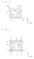
- FIG. 3 is a plan view showing a structure in which the fluid spraying portion 7 and the fluid sucking portion 17 are disposed in the semiconductor evaluating device 1 , and the insulating substrate 16 is omitted for easy understanding of the drawing.
- the single fluid spraying portion 7 is provided in an inclining state with respect to a vertical direction (to a Z direction), for example, in a corresponding position to an almost center of a single corner portion of the semiconductor device 5 in the insulating substrate 16 , and a fluid 20 is sprayed onto the whole front surface of the semiconductor device 5 by the fluid spraying portion 7 .
- the single fluid sucking portion 17 is provided in a corresponding position to an almost center of a corner portion which is opposed to the corner portion of the semiconductor device 5 in which the fluid spraying portion 7 is disposed in the insulating substrate 16 , and the fluid 20 sprayed onto the semiconductor device 5 is sucked by the fluid sucking portion 17 .
- the fluid sucking portion 17 is disposed in order to suppress pressurization of a measurement space which is limited in the semiconductor evaluating device 1 and to prevent the fluid 20 from scattering.
- the fluid spraying portion 7 is connected to a fluid supplying portion (not shown) through a fluid outlet pipe (not shown), and furthermore, the fluid sucking portion 17 is connected to the fluid supplying portion through a fluid inlet pipe (not shown) so that the fluid supplying portion is controlled by the control unit 4 .
- the control unit 4 controls the fluid supplying portion so as to start the evaluation for the electrical characteristic of the semiconductor device 5 , and at the same time, to start the supply of the fluid 20 from the fluid supplying portion to the fluid spraying portion 7 through the fluid outlet pipe and to start the suction of the fluid 20 by the fluid sucking portion 17 .
- the semiconductor device 5 is fixed onto the chuck stage 3 in such a manner that the installation surface of the semiconductor device 5 comes in contact with the chuck stage 3 .
- a semiconductor wafer having a plurality of semiconductor chips formed thereon or the semiconductor chip itself is proposed as the semiconductor device 5 , for example, the present invention is not restricted thereto but the semiconductor device 5 to be fixed by vacuum adsorption or the like is preferable.
- the contact probe 10 is caused to come in contact with the semiconductor device 5 through the connecting pad 18 .
- evaluation related to a desirable electrical characteristic is executed.
- the control unit 4 sprays the fluid 20 onto the front surface of the semiconductor device 5 by the fluid spraying portion 7 , and furthermore, sucks the sprayed fluid 20 by the fluid sucking portion 17 simultaneously with the start of the evaluation. Consequently, it is possible to maintain a state in which the atmospheric concentration of the fluid 20 is high in the vicinity of the front surface of the semiconductor device 5 during the evaluation.
- the control unit 4 ends the spraying and suction of the fluid 20 simultaneously with the end of the evaluation. Since the evaluation is executed in the state in which the atmospheric concentration of the fluid 20 is high, it is possible to effectively prevent a partial discharge from occurring in the vicinity of the front surface of the semiconductor device 5 .
- the semiconductor evaluating device 1 includes the chuck stage 3 for fixing the semiconductor device 5 which is the measuring object, the contact probe 10 for evaluating the electrical characteristic of the semiconductor device 5 by getting contact with the semiconductor device 5 fixed onto the chuck stage 3 through the connecting pad 18 , and the fluid spraying portion 7 for spraying the fluid 20 onto the semiconductor device 5 .
- the fluid 20 is sprayed onto the semiconductor device 5 by the fluid spraying portion 7 . Consequently, it is possible to easily prevent the partial discharge from occurring in the evaluation. Therefore, it is possible to enhance yield of the semiconductor device 5 .
- the fluid 20 is sprayed onto the semiconductor device 5 . For this reason, it is not necessary to tightly seal the measurement space in which the contact probe 10 and the semiconductor device 5 are provided. Moreover, it is not necessary to carry out additional processing for filling with the fluid 20 every evaluation or removing the fluid 20 from the semiconductor device 5 after the evaluation. Consequently, it is possible to reduce a cost and to prevent a time required for the evaluating process from being increased.
- the fluid sucking portion 17 is disposed in the opposed position to the fluid spraying portion 7 and serves to suck the fluid 20 sprayed by the fluid spraying portion 7 . Therefore, it is possible to prevent the sprayed fluid 20 from scattering, and furthermore, to suppress the pressurization of the measurement space.
- the insulating substrate 16 for installing the contact probe 10 thereon, and the fluid spraying portion 7 is disposed on the insulating substrate 16 .
- the insulating substrate 16 for installing the contact probe 10 and the fluid spraying portion 7 and the fluid sucking portion 17 are disposed on the insulating substrate 16 .
- the semiconductor device 5 By approaching the semiconductor device 5 to be the evaluation target to spray the fluid 20 thereonto, therefore, it is possible to enhance the effect for suppressing the partial discharge.
- By carrying out approach to suck the fluid 20 moreover, it is possible to efficiently prevent the sprayed fluid 20 from scattering, and furthermore, to efficiently suppress the pressurization of the measurement space.
- control unit 4 for starting to spray the fluid 20 by the fluid spraying portion 7 simultaneously with the start of the evaluation for the electrical characteristic of the semiconductor device 5 .
- the fluid 20 to be sprayed by the fluid spraying portion 7 is a sulfur hexafluoride gas, a carbon dioxide gas or a nitrogen gas. Therefore, it is possible to enhance the effect for suppressing the partial discharge.
- the fluid spraying portion 7 is provided in such a manner that the fluid 20 can be sprayed onto the whole surface of the semiconductor device 5 . Therefore, it is possible to efficiently spray the fluid 20 .
- the fluid spraying portion 7 may include a nozzle.
- a spraying port of the fluid spraying portion 7 may be formed to take a shape of the nozzle and may have a structure in which the fluid 20 is jetted at a high speed and reliably spreads over the front surface of the semiconductor device 5 . In this case, it is possible to efficiently spray the fluid 20 onto a target position in the semiconductor device 5 .
- the sucking port of the fluid sucking portion 17 may be wide, that is, may be formed as a cone-shaped sucking port to enhance sucking performance for the fluid 20 .
- FIG. 3 shows the example in which the single fluid spraying portion 7 and the single fluid sucking portion 17 are disposed respectively, furthermore, the present invention is not restricted thereto but it is also possible to employ a structure in which the plurality of fluid spraying portions 7 and the plurality of fluid sucking portions 17 are disposed to regulate the atmospheric concentration of the fluid 20 wholly or partially (for example, FIG. 4 which will be described below).
- FIG. 4 is a plan view showing a structure in which the fluid spraying portion 7 and the fluid sucking portion 17 are disposed in the semiconductor evaluating device 1 according to a first variant of the first preferred embodiment, and the insulating substrate 16 is omitted for easy understanding of the drawing.
- four fluid spraying portions 7 are disposed in corresponding positions to four corner portions of the semiconductor device 5 in the insulating substrate 16 respectively, and four fluid sucking portions 17 are disposed in corresponding positions to the opposed corner portions to the corner portions of the semiconductor device 5 in which the fluid spraying portions 7 are provided in the insulating substrate 16 respectively.
- the fluid spraying portion 7 and the fluid sucking portion 17 are shown to overlap with each other. As shown in FIG. 1 , however, the fluid spraying portion 7 sprays the fluid 20 from obliquely above the semiconductor device 5 toward the outer edge portion on one of sides of the semiconductor device 5 , and the fluid sucking portion 17 sucks the fluid 20 in the vicinity of the front surface of the semiconductor device 5 . Consequently, height positions in which the fluid spraying portion 7 and the fluid sucking portion 17 are to be provided are different from each other. For this reason, in the disposition, the fluid spraying portion 7 and the fluid sucking portion 17 do not interfere with each other.
- the fluid spraying portion 7 is provided in such a manner that the fluid 20 can be sprayed onto the outer edge portion of the semiconductor device 5 . Therefore, it is possible to particularly prevent the partial discharge from often occurring in the vicinity of the termination portion of the semiconductor device 5 .
- the present invention is not restricted thereto but a contact probe of a cantilever type may be employed (for example, the structure shown in FIG. 5 ).
- the contact probe having the sliding property in the Z-axis direction is not restricted to the spring type but may be a lamination probe, a wire probe or the like.
- FIG. 5 is a front view showing a structure in which the fluid spraying portion 7 is disposed in the semiconductor evaluating device 1 according to a second variant of the first preferred embodiment.
- a printed circuit board is employed as the insulating substrate 16 .
- Probe pins 10 a and 10 b constituting the contact probe 10 A are fixed to a lower surface of the insulating substrate 16 at a predetermined interval in an inclining state with respect to the vertical direction (the Z direction), respectively.
- base ends of the probe pins 10 a and 10 b are fixed to an outer peripheral part of a bored portion 16 a formed on the insulating substrate 16 , and the semiconductor device 5 is provided on tip sides of the probe pins 10 a and 10 b .
- the fluid spraying portion 7 is disposed on an upper side of the bored portion 16 a , and the fluid spraying portion 7 sprays the fluid 20 onto the whole front surface of the semiconductor device 5 through the bored portion 16 a.
- a temperature of the fluid 20 should be almost coincident with that of the semiconductor device 5 in the evaluation.
- a temperature characteristic is evaluated. In some cases, therefore, the temperature ranges from a low temperature to a high temperature, more specifically, approximately ⁇ 40° C. to +200° C., for example. For this reason, In the case where the temperature of the fluid 20 which is to be given in the evaluation is different from that of the semiconductor device 5 , the fluid 20 is sprayed so that the temperature of the semiconductor device 5 becomes unstable. As a result, desirable evaluation for the temperature characteristic cannot be obtained.
- FIG. 6 shows an example in which a first temperature control portion is added to the fluid spraying portion 7 .
- FIG. 6 is a front view showing a structure in which the fluid spraying portion 7 is disposed in the semiconductor evaluating device 1 according to a third variant of the first preferred embodiment.
- the first temperature control portion for controlling the temperature of the fluid 20 there is provided a heater portion 22 which is obtained by winding a heating wire like a coil upon the nozzle of the fluid spraying portion 7 .
- a current is applied to the heater portion 22 to control the temperature of the fluid spraying portion 7 , and furthermore, the temperature of the fluid 20 to be sprayed into a desirable value. Consequently, it is possible to suppress the instability of the temperature of the semiconductor device 5 which is caused by spraying the fluid 20 .
- the heater portion 22 controls the temperature of the fluid 20 to be equal to that of the semiconductor device 5 at the time of the evaluation for the electrical characteristic of the semiconductor device 5 , it is possible to suppress the instability of the temperature of the semiconductor device 5 still more by spraying the fluid 20 .
- the heater portion 22 is shown as an example of the first temperature control portion, the present invention is not restricted thereto but it is also possible to carry out heating by using a heater portion obtained by winding a near infrared wire like a coil. Moreover, it is also possible to employ a structure for taking a countermeasure against a low temperature by adding a Peltier element.
- FIG. 7 is a plan view showing a structure in which the fluid spraying portion 7 and the fluid sucking portion 17 are disposed in the semiconductor evaluating device 1 according to a fourth variant of the first preferred embodiment.
- the insulating substrate 16 is omitted for easy understanding of the drawing, and the fluid spraying portion 7 and the fluid sucking portion 17 are shown only in the outer edge portion on one of the sides in the semiconductor device 5 .
- the shielding portion 23 is formed in such a way as to take a shape of a frame as seen on a plane and is provided in a corresponding position to the outer edge portion of the semiconductor device 5 in the insulating substrate 16 in order to surround the element portion of the semiconductor device 5 .
- the fluid spraying portion 7 is disposed in a corresponding position to a predetermined corner portion of the semiconductor device 5 in the insulating substrate 16
- the fluid sucking portion 17 is disposed in a corresponding position to an opposed corner portion to the corner portion of the semiconductor device 5 in which the fluid spraying portion 7 is provided in the insulating substrate 16 .
- the flow of the fluid 20 sprayed by the fluid spraying portion 7 from the outer edge portion of the semiconductor device 5 into an inside of the outer edge portion of the semiconductor device 5 is shielded by the shielding portion 23 and is generally sprayed onto the outer edge portion of the semiconductor device 5 .
- the insulating substrate 16 is provided with the shielding portion 23 for shielding the flow of the fluid 20 sprayed by the fluid spraying portion 7 from the outer edge portion of the semiconductor device 5 into the inside of the outer edge portion of the semiconductor device 5 . Therefore, it is possible to prevent the fluid 20 from being sprayed onto the element portion of the semiconductor device 5 . Thus, it is possible to suppress a variation in temperature of the element portion of the semiconductor device 5 .
- the shielding portion 23 is formed by a metal plate or an insulator, for example. For this reason, In the case where the shielding portion 23 is formed by the metal plate, processing is easy to perform, and furthermore, a heat moving effect is enhanced. In the case where the shielding portion 23 is formed by the insulator, a heat capacity is large and a heat shielding effect is excellent.
- a second temperature control portion for controlling the temperature of the shielding portion 23 .
- the second temperature control portion a structure in which a heater portion obtained by winding a heating wire or a near infrared wire like a coil and a Peltier element are added in the same manner as in the first temperature control portion.
- the shielding portion 23 is provided with the second temperature control portion for controlling the temperature of the shielding portion 23 , it is possible to suppress a variation in temperature of the element portion, thereby enhancing the heat shielding effect by setting the temperature of the fluid 20 to be almost equal to that of the element portion through the second temperature control portion also when the fluid 20 passes through the shielding portion 23 and thus flows into the element portion of the semiconductor device 5 .
- the number of the shielding portions 23 is not restricted to be one but may be disposed in double or triple, for example, on the outer peripheral side of the shielding portion 23 in order to maintain the temperature of the element portion of the semiconductor device 5 with high precision so as not to be influenced by the temperature of the fluid 20 .
- FIG. 8 is a plan view showing a structure in which the fluid spraying portion 7 and the fluid sucking portion 17 are disposed in the semiconductor evaluating device 1 according to a fifth variant of the first preferred embodiment.
- the fluid spraying portion 7 and the fluid sucking portion 17 are provided in the same positions as those in FIG. 7 . Also in this case, it is possible to prevent the fluid 20 from being sprayed onto the element portion of the semiconductor device 5 by the shielding portion 24 . Consequently, it is possible to prevent the temperature of the element portion from being varied.
- FIG. 9 is a schematic view showing the semiconductor evaluating device 1 A according to the second preferred embodiment, illustrating the semiconductor evaluating device 1 A having a so-called double-sided probe structure in which a contact probe 10 is caused to come in contact from both front and back surfaces of a semiconductor device 5 .
- the same components as those described in the first preferred embodiment have the same reference numerals and description will be omitted.
- the semiconductor evaluating device 1 A includes a probe substrate 2 , a fluid spraying portion 7 , a fluid sucking portion 17 and a moving arm 9 which are provided on the front surface side and the back face side of the semiconductor device 5 , respectively, a control unit 4 , and a chuck stage 3 A for fixing both ends in an X direction of the semiconductor device 5 , respectively.
- FIG. 9 shows an example in which the semiconductor device 5 is provided in a horizontal direction (the X direction), the present invention is not restricted thereto but the semiconductor device 5 may be disposed in a vertical direction (in a Z direction).
- the contact probe 10 and the fluid spraying portion 7 are provided on the both front and back surface sides of the semiconductor device 5 . Therefore, it is possible to spray a fluid onto the whole front and back surfaces of the semiconductor device 5 . Consequently, it is also possible to prevent a partial discharge from occurring in the back surface of the semiconductor device 5 in addition to the front surface thereof.
- the fluid sucking portion 17 for sucking a fluid 20 sprayed by the fluid spraying portion 7 is provided in each of positions opposed to the fluid spraying portion 7 on both front and back surface sides of the semiconductor device 5 . Also at the back surface of the semiconductor device 5 in addition to the front surface thereof, therefore, it is possible to suck the fluid 20 , to efficiently prevent the sprayed fluid 20 from scattering, and furthermore, to efficiently suppress pressurization of a measurement space.
- FIG. 10 is a schematic view showing the semiconductor evaluating device 1 B according to the third preferred embodiment.
- FIG. 11 is a plan view showing a structure in which a fluid spraying portion 7 is disposed in the semiconductor evaluating device 1 B according to the third preferred embodiment.
- an insulating substrate 16 is omitted.
- FIG. 12 is a view for explaining an operation of a contact probe 10 in the semiconductor evaluating device 1 B according to the third preferred embodiment, and part (a) of FIG. 12 shows an initial state, part (b) of FIG. 12 shows a contact state and part (c) of FIG. 12 shows a pressing state.
- the same components as those described in the first and second preferred embodiments have the same reference numerals and description will be omitted.
- the fluid spraying portions 7 are provided in adjacent positions to the contact probes 10 , respectively, in a downward direction (in a ⁇ Z direction) in the insulating substrate 16 .
- the fluid spraying portion 7 includes a nozzle and serves to spray a fluid 20 in the downward direction (in the ⁇ Z direction).
- the fluid spraying portions 7 are provided in order to spray the fluid 20 onto the whole front surface of the semiconductor device 5 .
- a tip of the nozzle of the fluid spraying portion 7 has a height which is not equal to that of a contact portion 11 serving as a tip portion of the contact probe 10 . More specifically, the tip of the nozzle of the fluid spraying portion 7 is positioned above the contact portion 11 .
- the contact portion 11 comes in contact with a connecting pad 18 as shown in part (b) of FIG. 12 , and the tip of the nozzle is then positioned in the vicinity of an upper surface of the connecting pad 18 in the pressing state brought by the contact portion 11 shown in part (c) of FIG. 12 .
- the contact probe 10 and the fluid spraying portion 7 are provided to leave an interval in a horizontal direction (in an X direction) in such a manner that the contact portion 11 and the nozzle do not come in contact with each other.
- the fluid spraying portion 7 is disposed in an adjacent position to the contact probe 10 in the insulating substrate 16 . Therefore, it is possible to selectively prevent a partial discharge from occurring in the vicinity of the contact probe 10 .
- FIG. 13 is a plan view showing a structure in which the fluid spraying portion 7 is disposed in a semiconductor evaluating device according to a first variant of the third preferred embodiment.
- the insulating substrate 16 is omitted.
- the fluid spraying portion 7 is especially provided in a corresponding position to the peripheral edge portion of the semiconductor device 5 in the insulating substrate 16 , and four fluid spraying portions 7 are disposed in corresponding positions to respective sides of the semiconductor device 5 in the insulating substrate 16 .
- the fluid spraying portion 7 is disposed in a downward direction (a ⁇ Z direction) in the insulating substrate 16 in the same manner as in the case of FIG. 11 .
- the number of the fluid spraying portions 7 to be disposed in the corresponding positions to the respective sides of the semiconductor device 5 in the insulating substrate 16 is not restricted to be four but may be varied depending on a size of the semiconductor device 5 or precision of measurement.
Landscapes
- Engineering & Computer Science (AREA)
- Physics & Mathematics (AREA)
- General Physics & Mathematics (AREA)
- Computer Hardware Design (AREA)
- Microelectronics & Electronic Packaging (AREA)
- General Engineering & Computer Science (AREA)
- Testing Or Measuring Of Semiconductors Or The Like (AREA)
- Testing Of Individual Semiconductor Devices (AREA)
- Measuring Leads Or Probes (AREA)
Applications Claiming Priority (2)
| Application Number | Priority Date | Filing Date | Title |
|---|---|---|---|
| JP2013-013046 | 2013-01-28 | ||
| JP2013013046A JP6084469B2 (ja) | 2013-01-28 | 2013-01-28 | 半導体評価装置および半導体評価方法 |
Publications (2)
| Publication Number | Publication Date |
|---|---|
| US20140210500A1 US20140210500A1 (en) | 2014-07-31 |
| US9335371B2 true US9335371B2 (en) | 2016-05-10 |
Family
ID=51222223
Family Applications (1)
| Application Number | Title | Priority Date | Filing Date |
|---|---|---|---|
| US14/065,064 Active 2034-04-21 US9335371B2 (en) | 2013-01-28 | 2013-10-28 | Semiconductor evaluating device and semiconductor evaluating method |
Country Status (3)
| Country | Link |
|---|---|
| US (1) | US9335371B2 (enExample) |
| JP (1) | JP6084469B2 (enExample) |
| CN (1) | CN103969565B (enExample) |
Families Citing this family (17)
| Publication number | Priority date | Publication date | Assignee | Title |
|---|---|---|---|---|
| JP6218718B2 (ja) * | 2014-10-22 | 2017-10-25 | 三菱電機株式会社 | 半導体評価装置及びその評価方法 |
| JP6351763B2 (ja) * | 2015-01-23 | 2018-07-04 | 三菱電機株式会社 | 半導体装置評価用治具、半導体装置評価装置および半導体装置評価方法 |
| JP6386923B2 (ja) * | 2015-01-26 | 2018-09-05 | 三菱電機株式会社 | 半導体評価装置およびチャックステージの検査方法 |
| TWI530700B (zh) | 2015-03-11 | 2016-04-21 | 旺矽科技股份有限公司 | 測試機台及其操作方法 |
| JP2017009449A (ja) * | 2015-06-23 | 2017-01-12 | 三菱電機株式会社 | コンタクトプローブ型温度検出器、半導体装置の評価装置および半導体装置の評価方法 |
| JP6504971B2 (ja) * | 2015-08-20 | 2019-04-24 | 三菱電機株式会社 | 半導体チップテスト装置および半導体チップテスト方法 |
| JP6418118B2 (ja) * | 2015-09-24 | 2018-11-07 | 三菱電機株式会社 | 半導体装置の評価装置及び評価方法 |
| JP6478891B2 (ja) * | 2015-10-07 | 2019-03-06 | 三菱電機株式会社 | プローブ位置検査装置 |
| JP6515819B2 (ja) * | 2016-01-08 | 2019-05-22 | 三菱電機株式会社 | 評価装置、プローブ位置の検査方法 |
| JP2017129395A (ja) * | 2016-01-19 | 2017-07-27 | 三菱電機株式会社 | 半導体装置の検査装置および半導体装置の検査方法 |
| JP6593251B2 (ja) * | 2016-05-19 | 2019-10-23 | 三菱電機株式会社 | 半導体検査装置 |
| JP6562896B2 (ja) * | 2016-12-22 | 2019-08-21 | 三菱電機株式会社 | 半導体装置の評価装置およびそれを用いた半導体装置の評価方法 |
| JP6739326B2 (ja) * | 2016-12-27 | 2020-08-12 | 三菱電機株式会社 | 評価装置及び評価方法 |
| CN108535620A (zh) * | 2017-03-02 | 2018-09-14 | 叶秀慧 | 应用静电载具测试半导体制品的机构 |
| JP6822991B2 (ja) * | 2018-02-20 | 2021-01-27 | 株式会社東芝 | 可動端子装置と可動端子の出力を検出する装置 |
| US11378619B2 (en) * | 2019-12-18 | 2022-07-05 | Formfactor, Inc. | Double-sided probe systems with thermal control systems and related methods |
| CN114563677B (zh) * | 2022-03-01 | 2025-06-17 | 扬州扬杰电子科技股份有限公司 | 贴片二极管全自动检测装置 |
Citations (19)
| Publication number | Priority date | Publication date | Assignee | Title |
|---|---|---|---|---|
| JPS6165174A (ja) | 1984-09-06 | 1986-04-03 | Hitachi Electronics Eng Co Ltd | 電子部品加熱装置 |
| JPH0322454A (ja) | 1989-06-19 | 1991-01-30 | Nec Corp | 半導体検査装置 |
| JPH1096746A (ja) | 1996-09-25 | 1998-04-14 | Nakanihon Denshi Kk | 大電流用小型接触子 |
| JPH10319075A (ja) | 1997-05-16 | 1998-12-04 | U H T Kk | B・g・a、p・g・a等のicパッケージ用の基板の導通検査方法及びその装置 |
| JP2000164648A (ja) | 1998-11-25 | 2000-06-16 | Miyazaki Oki Electric Co Ltd | 電気的特性測定用装置および電気的特性測定方法 |
| US6248169B1 (en) * | 1999-06-01 | 2001-06-19 | Taiwan Semiconductor Manufacturing Company, Ltd. | Dual-cup coating apparatus |
| JP2002022770A (ja) | 2000-07-07 | 2002-01-23 | Micronics Japan Co Ltd | プローブカード |
| JP2003130889A (ja) | 2001-10-29 | 2003-05-08 | Vector Semicon Kk | 半導体装置検査装置及び検査方法 |
| JP2004111442A (ja) | 2002-09-13 | 2004-04-08 | Fujitsu Ltd | 半導体検査装置 |
| US6741445B1 (en) * | 2002-01-16 | 2004-05-25 | Advanced Micro Devices, Inc. | Method and system to monitor and control electro-static discharge |
| CN1536636A (zh) | 2003-04-08 | 2004-10-13 | 力晶半导体股份有限公司 | 晶圆表面离子取样系统及方法 |
| US20050000549A1 (en) * | 2003-07-03 | 2005-01-06 | Oikari James R. | Wafer processing using gaseous antistatic agent during drying phase to control charge build-up |
| JP2005030829A (ja) | 2003-07-09 | 2005-02-03 | Seiko Epson Corp | プッシャおよび半導体装置の特性検査装置 |
| JP2006337359A (ja) | 2005-05-02 | 2006-12-14 | Daytona Control Co Ltd | 温度制御装置 |
| US20070247177A1 (en) | 2006-04-19 | 2007-10-25 | Friedrich Ruckenbauer | Test Apparatus For Semiconductor Elements On A Semiconductor Wafer, And A Test Method Using The Test Apparatus |
| CN101113957A (zh) | 2006-07-27 | 2008-01-30 | 奥林巴斯株式会社 | 基板检查装置及基板检查装置使用的灯单元 |
| US20110017134A1 (en) * | 2007-11-07 | 2011-01-27 | Akihiko Tanioka | Immobilization apparatus |
| JP2011252792A (ja) | 2010-06-02 | 2011-12-15 | Fuji Electric Co Ltd | 試験装置および試験方法 |
| US20130229188A1 (en) * | 2012-03-01 | 2013-09-05 | Neuronexus Technologies, Inc. | System and method for testing electrical circuits using a photoelectrochemical effect |
-
2013
- 2013-01-28 JP JP2013013046A patent/JP6084469B2/ja not_active Expired - Fee Related
- 2013-10-28 US US14/065,064 patent/US9335371B2/en active Active
-
2014
- 2014-01-28 CN CN201410042200.3A patent/CN103969565B/zh active Active
Patent Citations (22)
| Publication number | Priority date | Publication date | Assignee | Title |
|---|---|---|---|---|
| JPS6165174A (ja) | 1984-09-06 | 1986-04-03 | Hitachi Electronics Eng Co Ltd | 電子部品加熱装置 |
| JPH0322454A (ja) | 1989-06-19 | 1991-01-30 | Nec Corp | 半導体検査装置 |
| JPH1096746A (ja) | 1996-09-25 | 1998-04-14 | Nakanihon Denshi Kk | 大電流用小型接触子 |
| JPH10319075A (ja) | 1997-05-16 | 1998-12-04 | U H T Kk | B・g・a、p・g・a等のicパッケージ用の基板の導通検査方法及びその装置 |
| JP2000164648A (ja) | 1998-11-25 | 2000-06-16 | Miyazaki Oki Electric Co Ltd | 電気的特性測定用装置および電気的特性測定方法 |
| US6248169B1 (en) * | 1999-06-01 | 2001-06-19 | Taiwan Semiconductor Manufacturing Company, Ltd. | Dual-cup coating apparatus |
| JP2002022770A (ja) | 2000-07-07 | 2002-01-23 | Micronics Japan Co Ltd | プローブカード |
| JP2003130889A (ja) | 2001-10-29 | 2003-05-08 | Vector Semicon Kk | 半導体装置検査装置及び検査方法 |
| US6741445B1 (en) * | 2002-01-16 | 2004-05-25 | Advanced Micro Devices, Inc. | Method and system to monitor and control electro-static discharge |
| JP2004111442A (ja) | 2002-09-13 | 2004-04-08 | Fujitsu Ltd | 半導体検査装置 |
| CN1536636A (zh) | 2003-04-08 | 2004-10-13 | 力晶半导体股份有限公司 | 晶圆表面离子取样系统及方法 |
| US20050000549A1 (en) * | 2003-07-03 | 2005-01-06 | Oikari James R. | Wafer processing using gaseous antistatic agent during drying phase to control charge build-up |
| JP2005030829A (ja) | 2003-07-09 | 2005-02-03 | Seiko Epson Corp | プッシャおよび半導体装置の特性検査装置 |
| JP2006337359A (ja) | 2005-05-02 | 2006-12-14 | Daytona Control Co Ltd | 温度制御装置 |
| US20070247177A1 (en) | 2006-04-19 | 2007-10-25 | Friedrich Ruckenbauer | Test Apparatus For Semiconductor Elements On A Semiconductor Wafer, And A Test Method Using The Test Apparatus |
| CN101113957A (zh) | 2006-07-27 | 2008-01-30 | 奥林巴斯株式会社 | 基板检查装置及基板检查装置使用的灯单元 |
| US20080049218A1 (en) | 2006-07-27 | 2008-02-28 | Olympus Corporation | Substrate inspection device and lamp unit used therein |
| US20110017134A1 (en) * | 2007-11-07 | 2011-01-27 | Akihiko Tanioka | Immobilization apparatus |
| JP2011252792A (ja) | 2010-06-02 | 2011-12-15 | Fuji Electric Co Ltd | 試験装置および試験方法 |
| US20110309850A1 (en) | 2010-06-02 | 2011-12-22 | Fuji Electric Co., Ltd. | Testing device and testing method |
| US8610446B2 (en) | 2010-06-02 | 2013-12-17 | Fuji Electric Co., Ltd. | Testing device and testing method |
| US20130229188A1 (en) * | 2012-03-01 | 2013-09-05 | Neuronexus Technologies, Inc. | System and method for testing electrical circuits using a photoelectrochemical effect |
Non-Patent Citations (2)
| Title |
|---|
| An Office Action; "Notification of Reason(s) for Refusal," issued by the Japanese Patent Office on Mar. 1, 2016, which corresponds to Japanese Patent Application No. 2013-013046 and is related to U.S. Appl. No. 14/065,064; with English language translation. |
| The First Office Action issued by the Chinese Patent Office on Jan. 21, 2016, which corresponds to Chinese Patent Application No. 201410042200.3 and is related to U.S. Appl. No. 14/065,064; with English language translation. |
Also Published As
| Publication number | Publication date |
|---|---|
| CN103969565A (zh) | 2014-08-06 |
| CN103969565B (zh) | 2016-12-07 |
| US20140210500A1 (en) | 2014-07-31 |
| JP6084469B2 (ja) | 2017-02-22 |
| JP2014145615A (ja) | 2014-08-14 |
Similar Documents
| Publication | Publication Date | Title |
|---|---|---|
| US9335371B2 (en) | Semiconductor evaluating device and semiconductor evaluating method | |
| US9678143B2 (en) | Semiconductor evaluation apparatus | |
| TWI631353B (zh) | Probe device | |
| CN108254667B (zh) | 评价装置及评价方法 | |
| US11428727B2 (en) | Prober | |
| JP5016892B2 (ja) | 検査装置及び検査方法 | |
| CN106935524A (zh) | 探针卡和晶圆测试系统及晶圆测试方法 | |
| JP6365953B1 (ja) | プローバ | |
| US20140184259A1 (en) | Method and device for testing wafers | |
| KR20090009707A (ko) | 검사 장치, 프로브 카드 및 검사 방법 | |
| JP6045993B2 (ja) | プローブ装置 | |
| US20160146882A1 (en) | Method of contacting integrated circuit components in a test system | |
| JP2016211977A (ja) | 半導体チップの試験装置及び試験方法 | |
| US9684015B2 (en) | Measuring apparatus and measuring method utilizing insulating liquid | |
| KR101500609B1 (ko) | 검사장치 | |
| KR101182361B1 (ko) | 반도체소자 캐리어유닛 | |
| CN102593106A (zh) | 一种用于防止封装样品被静电损伤的保护装置 | |
| US10725086B2 (en) | Evaluation apparatus of semiconductor device and method of evaluating semiconductor device using the same | |
| JP6686825B2 (ja) | 評価装置、半導体装置の評価方法 | |
| JP6731862B2 (ja) | 半導体装置の評価装置 | |
| US20240295599A1 (en) | Semiconductor testing apparatus and method of manufacturing semiconductor device | |
| KR200414883Y1 (ko) | 반도체소자 캐리어 유닛 | |
| KR101182362B1 (ko) | 반도체소자 캐리어유닛 | |
| JP2024062542A (ja) | 半導体装置および半導体装置の検査方法 | |
| JP2022159793A (ja) | 半導体テスト装置および半導体装置の製造方法 |
Legal Events
| Date | Code | Title | Description |
|---|---|---|---|
| AS | Assignment |
Owner name: MITSUBISHI ELECTRIC CORPORATION, JAPAN Free format text: ASSIGNMENT OF ASSIGNORS INTEREST;ASSIGNORS:AKIYAMA, HAJIME;OKADA, AKIRA;YAMASHITA, KINYA;REEL/FRAME:031492/0624 Effective date: 20130821 |
|
| STCF | Information on status: patent grant |
Free format text: PATENTED CASE |
|
| MAFP | Maintenance fee payment |
Free format text: PAYMENT OF MAINTENANCE FEE, 4TH YEAR, LARGE ENTITY (ORIGINAL EVENT CODE: M1551); ENTITY STATUS OF PATENT OWNER: LARGE ENTITY Year of fee payment: 4 |
|
| MAFP | Maintenance fee payment |
Free format text: PAYMENT OF MAINTENANCE FEE, 8TH YEAR, LARGE ENTITY (ORIGINAL EVENT CODE: M1552); ENTITY STATUS OF PATENT OWNER: LARGE ENTITY Year of fee payment: 8 |