US9245742B2 - Sulfur-containing thin films - Google Patents
Sulfur-containing thin films Download PDFInfo
- Publication number
- US9245742B2 US9245742B2 US14/133,509 US201314133509A US9245742B2 US 9245742 B2 US9245742 B2 US 9245742B2 US 201314133509 A US201314133509 A US 201314133509A US 9245742 B2 US9245742 B2 US 9245742B2
- Authority
- US
- United States
- Prior art keywords
- metal
- sulfur
- reactant
- precursor
- thin film
- Prior art date
- Legal status (The legal status is an assumption and is not a legal conclusion. Google has not performed a legal analysis and makes no representation as to the accuracy of the status listed.)
- Active
Links
Images


Classifications
-
- H01L21/02175—
-
- H—ELECTRICITY
- H10—SEMICONDUCTOR DEVICES; ELECTRIC SOLID-STATE DEVICES NOT OTHERWISE PROVIDED FOR
- H10P—GENERIC PROCESSES OR APPARATUS FOR THE MANUFACTURE OR TREATMENT OF DEVICES COVERED BY CLASS H10
- H10P14/00—Formation of materials, e.g. in the shape of layers or pillars
- H10P14/60—Formation of materials, e.g. in the shape of layers or pillars of insulating materials
- H10P14/69—Inorganic materials
- H10P14/692—Inorganic materials composed of oxides, glassy oxides or oxide-based glasses
- H10P14/6938—Inorganic materials composed of oxides, glassy oxides or oxide-based glasses the material containing at least one metal element, e.g. metal oxides, metal oxynitrides or metal oxycarbides
- H10P14/6939—Inorganic materials composed of oxides, glassy oxides or oxide-based glasses the material containing at least one metal element, e.g. metal oxides, metal oxynitrides or metal oxycarbides characterised by the metal
-
- H01L21/02192—
-
- H01L21/02194—
-
- H01L21/0228—
-
- H01L21/02334—
-
- H01L21/0237—
-
- H01L21/02557—
-
- H01L21/02568—
-
- H01L21/0262—
-
- H01L21/02661—
-
- H—ELECTRICITY
- H10—SEMICONDUCTOR DEVICES; ELECTRIC SOLID-STATE DEVICES NOT OTHERWISE PROVIDED FOR
- H10D—INORGANIC ELECTRIC SEMICONDUCTOR DEVICES
- H10D30/00—Field-effect transistors [FET]
- H10D30/40—FETs having zero-dimensional [0D], one-dimensional [1D] or two-dimensional [2D] charge carrier gas channels
- H10D30/47—FETs having zero-dimensional [0D], one-dimensional [1D] or two-dimensional [2D] charge carrier gas channels having two-dimensional [2D] charge carrier gas channels, e.g. nanoribbon FETs or high electron mobility transistors [HEMT]
- H10D30/471—High electron mobility transistors [HEMT] or high hole mobility transistors [HHMT]
- H10D30/475—High electron mobility transistors [HEMT] or high hole mobility transistors [HHMT] having wider bandgap layer formed on top of lower bandgap active layer, e.g. undoped barrier HEMTs such as i-AlGaN/GaN HEMTs
-
- H—ELECTRICITY
- H10—SEMICONDUCTOR DEVICES; ELECTRIC SOLID-STATE DEVICES NOT OTHERWISE PROVIDED FOR
- H10D—INORGANIC ELECTRIC SEMICONDUCTOR DEVICES
- H10D62/00—Semiconductor bodies, or regions thereof, of devices having potential barriers
- H10D62/80—Semiconductor bodies, or regions thereof, of devices having potential barriers characterised by the materials
- H10D62/82—Heterojunctions
-
- H—ELECTRICITY
- H10—SEMICONDUCTOR DEVICES; ELECTRIC SOLID-STATE DEVICES NOT OTHERWISE PROVIDED FOR
- H10D—INORGANIC ELECTRIC SEMICONDUCTOR DEVICES
- H10D64/00—Electrodes of devices having potential barriers
- H10D64/01—Manufacture or treatment
- H10D64/013—Manufacture or treatment of electrodes having a conductor capacitively coupled to a semiconductor by an insulator
- H10D64/01358—Manufacture or treatment of electrodes having a conductor capacitively coupled to a semiconductor by an insulator the insulator being formed after the semiconductor body, the semiconductor being a Group III-V material
-
- H—ELECTRICITY
- H10—SEMICONDUCTOR DEVICES; ELECTRIC SOLID-STATE DEVICES NOT OTHERWISE PROVIDED FOR
- H10P—GENERIC PROCESSES OR APPARATUS FOR THE MANUFACTURE OR TREATMENT OF DEVICES COVERED BY CLASS H10
- H10P14/00—Formation of materials, e.g. in the shape of layers or pillars
- H10P14/20—Formation of materials, e.g. in the shape of layers or pillars of semiconductor materials
- H10P14/24—Formation of materials, e.g. in the shape of layers or pillars of semiconductor materials using chemical vapour deposition [CVD]
-
- H—ELECTRICITY
- H10—SEMICONDUCTOR DEVICES; ELECTRIC SOLID-STATE DEVICES NOT OTHERWISE PROVIDED FOR
- H10P—GENERIC PROCESSES OR APPARATUS FOR THE MANUFACTURE OR TREATMENT OF DEVICES COVERED BY CLASS H10
- H10P14/00—Formation of materials, e.g. in the shape of layers or pillars
- H10P14/20—Formation of materials, e.g. in the shape of layers or pillars of semiconductor materials
- H10P14/29—Formation of materials, e.g. in the shape of layers or pillars of semiconductor materials characterised by the substrates
- H10P14/2901—Materials
-
- H—ELECTRICITY
- H10—SEMICONDUCTOR DEVICES; ELECTRIC SOLID-STATE DEVICES NOT OTHERWISE PROVIDED FOR
- H10P—GENERIC PROCESSES OR APPARATUS FOR THE MANUFACTURE OR TREATMENT OF DEVICES COVERED BY CLASS H10
- H10P14/00—Formation of materials, e.g. in the shape of layers or pillars
- H10P14/20—Formation of materials, e.g. in the shape of layers or pillars of semiconductor materials
- H10P14/34—Deposited materials, e.g. layers
- H10P14/3402—Deposited materials, e.g. layers characterised by the chemical composition
- H10P14/3424—Deposited materials, e.g. layers characterised by the chemical composition being Group IIB-VIA materials
- H10P14/3428—Sulfides
-
- H—ELECTRICITY
- H10—SEMICONDUCTOR DEVICES; ELECTRIC SOLID-STATE DEVICES NOT OTHERWISE PROVIDED FOR
- H10P—GENERIC PROCESSES OR APPARATUS FOR THE MANUFACTURE OR TREATMENT OF DEVICES COVERED BY CLASS H10
- H10P14/00—Formation of materials, e.g. in the shape of layers or pillars
- H10P14/20—Formation of materials, e.g. in the shape of layers or pillars of semiconductor materials
- H10P14/34—Deposited materials, e.g. layers
- H10P14/3402—Deposited materials, e.g. layers characterised by the chemical composition
- H10P14/3436—Deposited materials, e.g. layers characterised by the chemical composition being chalcogenide semiconductor materials not being oxides, e.g. ternary compounds
-
- H—ELECTRICITY
- H10—SEMICONDUCTOR DEVICES; ELECTRIC SOLID-STATE DEVICES NOT OTHERWISE PROVIDED FOR
- H10P—GENERIC PROCESSES OR APPARATUS FOR THE MANUFACTURE OR TREATMENT OF DEVICES COVERED BY CLASS H10
- H10P14/00—Formation of materials, e.g. in the shape of layers or pillars
- H10P14/20—Formation of materials, e.g. in the shape of layers or pillars of semiconductor materials
- H10P14/36—Formation of materials, e.g. in the shape of layers or pillars of semiconductor materials characterised by treatments done before the formation of the materials
- H10P14/3602—In-situ cleaning
-
- H—ELECTRICITY
- H10—SEMICONDUCTOR DEVICES; ELECTRIC SOLID-STATE DEVICES NOT OTHERWISE PROVIDED FOR
- H10P—GENERIC PROCESSES OR APPARATUS FOR THE MANUFACTURE OR TREATMENT OF DEVICES COVERED BY CLASS H10
- H10P14/00—Formation of materials, e.g. in the shape of layers or pillars
- H10P14/60—Formation of materials, e.g. in the shape of layers or pillars of insulating materials
- H10P14/63—Formation of materials, e.g. in the shape of layers or pillars of insulating materials characterised by the formation processes
- H10P14/6326—Deposition processes
- H10P14/6328—Deposition from the gas or vapour phase
- H10P14/6334—Deposition from the gas or vapour phase using decomposition or reaction of gaseous or vapour phase compounds, i.e. chemical vapour deposition
- H10P14/6339—Deposition from the gas or vapour phase using decomposition or reaction of gaseous or vapour phase compounds, i.e. chemical vapour deposition deposition by cyclic CVD, e.g. ALD, ALE or pulsed CVD
-
- H—ELECTRICITY
- H10—SEMICONDUCTOR DEVICES; ELECTRIC SOLID-STATE DEVICES NOT OTHERWISE PROVIDED FOR
- H10P—GENERIC PROCESSES OR APPARATUS FOR THE MANUFACTURE OR TREATMENT OF DEVICES COVERED BY CLASS H10
- H10P14/00—Formation of materials, e.g. in the shape of layers or pillars
- H10P14/60—Formation of materials, e.g. in the shape of layers or pillars of insulating materials
- H10P14/65—Formation of materials, e.g. in the shape of layers or pillars of insulating materials characterised by treatments performed before or after the formation of the materials
- H10P14/6516—Formation of materials, e.g. in the shape of layers or pillars of insulating materials characterised by treatments performed before or after the formation of the materials of treatments performed after formation of the materials
- H10P14/6528—In-situ cleaning after layer formation, e.g. removing process residues
-
- H—ELECTRICITY
- H10—SEMICONDUCTOR DEVICES; ELECTRIC SOLID-STATE DEVICES NOT OTHERWISE PROVIDED FOR
- H10P—GENERIC PROCESSES OR APPARATUS FOR THE MANUFACTURE OR TREATMENT OF DEVICES COVERED BY CLASS H10
- H10P14/00—Formation of materials, e.g. in the shape of layers or pillars
- H10P14/60—Formation of materials, e.g. in the shape of layers or pillars of insulating materials
- H10P14/69—Inorganic materials
- H10P14/692—Inorganic materials composed of oxides, glassy oxides or oxide-based glasses
- H10P14/6938—Inorganic materials composed of oxides, glassy oxides or oxide-based glasses the material containing at least one metal element, e.g. metal oxides, metal oxynitrides or metal oxycarbides
- H10P14/6939—Inorganic materials composed of oxides, glassy oxides or oxide-based glasses the material containing at least one metal element, e.g. metal oxides, metal oxynitrides or metal oxycarbides characterised by the metal
- H10P14/69396—Inorganic materials composed of oxides, glassy oxides or oxide-based glasses the material containing at least one metal element, e.g. metal oxides, metal oxynitrides or metal oxycarbides characterised by the metal the material containing at least one rare earth metal element, e.g. oxides of lanthanides, scandium or yttrium
-
- H—ELECTRICITY
- H10—SEMICONDUCTOR DEVICES; ELECTRIC SOLID-STATE DEVICES NOT OTHERWISE PROVIDED FOR
- H10P—GENERIC PROCESSES OR APPARATUS FOR THE MANUFACTURE OR TREATMENT OF DEVICES COVERED BY CLASS H10
- H10P14/00—Formation of materials, e.g. in the shape of layers or pillars
- H10P14/60—Formation of materials, e.g. in the shape of layers or pillars of insulating materials
- H10P14/69—Inorganic materials
- H10P14/692—Inorganic materials composed of oxides, glassy oxides or oxide-based glasses
- H10P14/6938—Inorganic materials composed of oxides, glassy oxides or oxide-based glasses the material containing at least one metal element, e.g. metal oxides, metal oxynitrides or metal oxycarbides
- H10P14/6939—Inorganic materials composed of oxides, glassy oxides or oxide-based glasses the material containing at least one metal element, e.g. metal oxides, metal oxynitrides or metal oxycarbides characterised by the metal
- H10P14/69397—Inorganic materials composed of oxides, glassy oxides or oxide-based glasses the material containing at least one metal element, e.g. metal oxides, metal oxynitrides or metal oxycarbides characterised by the metal the material containing two or more metal elements
-
- H01L21/02395—
-
- H—ELECTRICITY
- H10—SEMICONDUCTOR DEVICES; ELECTRIC SOLID-STATE DEVICES NOT OTHERWISE PROVIDED FOR
- H10D—INORGANIC ELECTRIC SEMICONDUCTOR DEVICES
- H10D30/00—Field-effect transistors [FET]
- H10D30/01—Manufacture or treatment
- H10D30/021—Manufacture or treatment of FETs having insulated gates [IGFET]
- H10D30/024—Manufacture or treatment of FETs having insulated gates [IGFET] of fin field-effect transistors [FinFET]
-
- H—ELECTRICITY
- H10—SEMICONDUCTOR DEVICES; ELECTRIC SOLID-STATE DEVICES NOT OTHERWISE PROVIDED FOR
- H10D—INORGANIC ELECTRIC SEMICONDUCTOR DEVICES
- H10D30/00—Field-effect transistors [FET]
- H10D30/60—Insulated-gate field-effect transistors [IGFET]
-
- H—ELECTRICITY
- H10—SEMICONDUCTOR DEVICES; ELECTRIC SOLID-STATE DEVICES NOT OTHERWISE PROVIDED FOR
- H10D—INORGANIC ELECTRIC SEMICONDUCTOR DEVICES
- H10D62/00—Semiconductor bodies, or regions thereof, of devices having potential barriers
- H10D62/80—Semiconductor bodies, or regions thereof, of devices having potential barriers characterised by the materials
- H10D62/86—Semiconductor bodies, or regions thereof, of devices having potential barriers characterised by the materials being Group II-VI materials, e.g. ZnO
- H10D62/8603—Binary Group II-VI materials wherein cadmium is the Group II element, e.g. CdTe
-
- H—ELECTRICITY
- H10—SEMICONDUCTOR DEVICES; ELECTRIC SOLID-STATE DEVICES NOT OTHERWISE PROVIDED FOR
- H10P—GENERIC PROCESSES OR APPARATUS FOR THE MANUFACTURE OR TREATMENT OF DEVICES COVERED BY CLASS H10
- H10P14/00—Formation of materials, e.g. in the shape of layers or pillars
- H10P14/20—Formation of materials, e.g. in the shape of layers or pillars of semiconductor materials
- H10P14/29—Formation of materials, e.g. in the shape of layers or pillars of semiconductor materials characterised by the substrates
- H10P14/2901—Materials
- H10P14/2907—Materials being Group IIIA-VA materials
- H10P14/2911—Arsenides
Definitions
- the invention relates generally to the field of semiconductor device manufacturing and, more particularly, to metal sulfide films and methods for forming sulfur-containing thin films, such as by atomic layer deposition (“ALD”) processes.
- metal sulfide films such as MgS films may be formed by ALD processes and may serve as an interface layer between a substrate and a dielectric layer.
- high-mobility substrate materials such as germanium, which exhibits desirable hole mobility
- group III-V materials which exhibit desirable electron mobility
- Suitable group III-V materials include, for example, GaAs, InP, InGaAs, InAs, and GaSb.
- problems with these new channel materials can be present at the interface between the high-mobility material and the overlying dielectric layer.
- the high-mobility semiconducting channel based on materials such as Ge and InGaAs, have a very high number of interface states. These states tend to pin the Fermi energy and can severely deteriorate the function of electronic devices. Sulfur passivation can be an efficient approach to minimize the interface states. Beyond passivating the surface, an interface layer is desirable for integration with a high-k dielectric layer.
- known interface layers have a variety of problems, such as not preventing oxidation of the underlying high-mobility channel and allowing for undesirable current leakage or charge trapping and not preventing up diffusion of group III-V elements or Ge into the gate dielectric.
- a metal sulfide thin film is deposited on a substrate in a reaction space in a cyclical process where at least one cycle includes alternately and sequentially contacting the substrate with a first vapor-phase metal reactant and a second vapor-phase sulfur reactant.
- the metal reactant comprises a metal selected from the group consisting of Mg, Ca, Y, Sc, Sr, Ba, La, and other lanthanides.
- a method for forming a metal sulfide thin film includes removing excess vapor-phase metal reactant and reaction byproducts from the reaction space after contacting the substrate with the first vapor-phase metal reactant. In some embodiments, excess vapor-phase sulfur reactant and reaction byproducts from the reaction space after contacting the substrate with the second vapor-phase sulfur reactant. In some embodiments, the second reactant is introduced into the reaction space before introducing the vapor-phase metal reactant into the reaction space in at least one deposition cycle.
- the metal sulfide film is formed using a metal reactant having at least one cyclopentadienyl (Cp) ligand.
- the metal of the metal sulfide thin film is magnesium (Mg).
- the metal reactant is Mg(Cp) 2 or a derivative thereof.
- the metal reactant comprises Cp or a derivative thereof and the metal is Ca, La or another lanthanide, Sc, or Y.
- the metal reactant includes a metal that is not present in the portion of the substrate surface upon which the metal sulfide thin film is being formed.
- a method for forming a metal sulfide thin film includes H 2 S as a sulfur precursor or reactant.
- the second reactant, or sulfur precursor comprises sulfur atoms, sulfur-containing plasma, or sulfur-radicals.
- the resulting metal sulfide thin film comprises MgS.
- the substrate surface on which the metal sulfide film is deposited does not include silicon.
- the substrate surface comprises InGaAs.
- the metal sulfide thin film comprises more than one metal.
- the metal sulfide thin film comprises non-metals in addition to sulfur, such as oxygen or nitrogen.
- a method for forming a metal sulfide thin film includes subjecting the substrate to a pretreatment reactant either ex situ or in situ prior to depositing the metal sulfide thin film.
- the metal sulfide film is subjected to a post-treatment reactant after deposition.
- the metal sulfide thin film has a thickness of between about 1 ⁇ and about 20 ⁇ .
- the magneiusm sulfide thin film is formed on a substrate in a reaction space in one or more deposition cycles.
- the deposition cycles include providing a vapor-phase magnesium reactant to the reaction space, removing excess vapor-phase magnesium reactant and reaction by-products, providing a second reactant comprising sulfur to the reaction space, and removing excess second reactant and reaction by-products.
- the second reactant is provided to the reaction space before providing the vapor-phase magnesium reactant to the reaction space.
- the magnesium sulfide thin film comprises at least one metal other than magnesium.
- the magnesium sulfide film comprises at least one non-metal element other than sulfur, such as nitrogen or oxygen.
- methods of forming a three-dimensional architecture on a substrate surface include forming a metal sulfide thin film on the substrate surface and forming a capping layer over the metal sulfide thin film.
- the substrate surface comprises a high-mobility channel.
- the metal of the metal sulfide thin film comprises at least one of the following: beryllium, magnesium, calcium, strontium, scandium, yttrium, and lanthanum.
- a method of forming a three-dimensional architecture includes subjecting the substrate surface to a pretreatment process prior to forming a metal sulfide thin film on the substrate surface.
- the pretreatment process comprises subjecting the substrate surface to at least one of the following pretreatment reactants: (NH 4 ) 2 S, H 2 S, HCl, HBr, Cl 2 , and HF.
- the pretreatment process comprises exposing the substrate surface to at least one pretreatment reactant for a period of between about 1 second and about 600 seconds, preferably between about 1 second and about 60 seconds.
- a barrier layer is formed over the capping layer.
- Some embodiments include, after forming a capping layer over the metal sulfide thin film, forming a metal gate over the capping layer. Some embodiments include subjecting the metal sulfide thin film and the capping layer to a post deposition treatment comprising an annealing process or a gas forming process.
- the metal of the metal sulfide thin film is different from the metal or metals of the underlying substrate surface. In some embodiments, the metal of the metal sulfide thin film is different from the metal or metals of the subsequently formed capping layer. In some embodiments, the metal of the metal sulfide thin film is the same as at least one of the metal or metals of the subsequently formed capping layer. According to some embodiments, the capping layer comprises a high-k dielectric material. And in some embodiments, the substrate surface comprises a high-mobility channel.
- the metal of the metal sulfide thin film comprises at least one of the following metals: Be, Mg, Ca, Ba, Sr, Y, Sc, La, Ce, Pr, Nd, Pm, Sm, Eu, Gd, Tb, Dy, Ho, Er, Tm, Yb, Lu, Al, Si, Zn, Cd, Pb, In, Ga, Ge, Gd, Ta, Mo, and W.
- the metal sulfide thin film has a thickness between about 5 ⁇ and about 20 ⁇ .
- methods of forming a three-dimensional architecture on a substrate surface include forming a metal sulfide thin film on the substrate surface using an ALD process and forming a capping layer comprising a high-k dielectric material over the metal sulfide thin film.
- the metal of the metal sulfide thin film comprises at least one of the following metals: Be, Mg, Ca, Ba, Sr, Y, Sc, La, Ce, Pr, Nd, Pm, Sm, Eu, Gd, Tb, Dy, Ho, Er, Tm, Yb, Lu, Al, Si, Zn, Cd, Pb, In, Ga, Ge, Gd, Ta, Mo, and W.
- the metal sulfide thin film is formed using a sulfur precursor selected from the following: elemental sulfur, sulfur plasma, H 2 S, and (NH 4 ) 2 S.
- the method includes subjecting the substrate surface to a pretreatment process prior to forming a metal sulfide thin film on the substrate surface, wherein the pretreatment process comprises exposing the substrate surface to at least one of the following: HCl, HF, H 2 S, HBr, Cl 2 , and HF.
- the method includes subjecting the previously formed capping layer and metal sulfide thin film to a post deposition treatment, wherein the post deposition treatment comprises exposure to at least one of the following compounds or processes: HCl, HF, H 2 S, (NH 4 ) 2 S, H 2 plasma, NF 3 , thermal H 2 bake, and an annealing process.
- the metal of the metal sulfide thin film is different from one or both of the metal or metals of the underlying substrate surface and the metal or metals of the capping layer.
- the substrate surface comprises a high-mobility channel, wherein the high-mobility channel includes germanium or a III-V material.
- FIG. 1 is a schematic representation of a gate stack that includes an interfacial layer.
- FIG. 2 is a flow chart illustrating an ALD process for forming a metal sulfide thin film according to some embodiments.
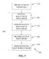
- FIG. 3 is a flow chart illustrating an ALD process for forming a magnesium sulfide thin film according to some embodiments.
- FIG. 4 illustrates an exemplary process for forming a three-dimensional architecture according to the present disclosure.
- FIG. 5 illustrates a capacitance vs. voltage curve with a frequency dispersion range from 100 Hz to 1 MHz for an interfacial layer.
- FIG. 6 illustrates a capacitance vs. voltage curve with a frequency dispersion range from 100 Hz to 1 MHz for a sulfur-containing thin film according to one embodiment of the present disclosure.
- metal sulfide films and methods of forming metal sulfide thin films are provided.
- the metal of the metal sulfide thin film may be selected from any number of metals, such as beryllium, magnesium, yttrium, calcium, strontium, barium, lanthanum and other lanthanides (such as cerium, praseodymium, neodymium, promethium, samarium, europium, gadolinium, terbium, dysprosium, holmium, erbium, thulium, ytterbium, and lutetium), silicon, zinc, cadmium, lead, indium, gallium, germanium, tantalum, molybdenum, and tungsten.
- metals such as beryllium, magnesium, yttrium, calcium, strontium, barium, lanthanum and other lanthanides (such as cerium, praseodymium, neodymium, prome
- a metal sulfide film is used as an interface layer, for example between a substrate and a dielectric layer.
- the interface layer comprises a part of a gate stack.
- the interface layer is located between a dielectric layer and a high-mobility channel.
- FIG. 1 illustrates a common gate stack configuration 100 that is formed on a substrate 110 .
- a high mobility channel 115 is located between a source 120 and a drain 130 .
- a metal sulfide interface layer 140 may be included between the high-mobility channel and the dielectric layer 150 .
- a metal gate 160 is present over the dielectric layer 150 .
- the metal sulfide interface layer 140 may be formed using the methods described herein.
- the metal in the metal sulfide thin film is chosen so as to be distinct from the metal in the underlying portion of the substrate.
- the metal in a metal sulfide film may be different from any metal in an underlying high-mobility channel.
- the metal in the metal sulfide film may be different from the metal in an overlying dielectric layer.
- a metal sulfide interlayer may comprise a metal that is different from any metal in an underlying channel region of the substrate and from an overlying dielectric layer.
- a metal sulfide interface layer comprises one or more of MgS, CaS, ScS x , YS x , LaS, a lanthanide sulfide, Al 2 S 3 , SiS 2 , ZnS, CdS, SrS, CaS, BaS, PbS, In 2 S 3 , Ga 2 S 3 , GeS 2 , Gd 2 S 3 , TaS 2 , MoS 2 and WS 2 .
- particular metals are expressly avoided, such as cesium and/or aluminum.
- suitable interfacial layers comprise a metal sulfide material that may protect the underlying high-mobility substrate material from undesirable oxidation.
- the metal sulfide thin film may be considered a passivation layer.
- gate stacks formed with the presently disclosed interfacial layers exhibit reduced leakage or reduced charge.
- metal sulfide films may be incorporated into a variety of integrated circuit architectures, such as FINFETs, planar transistors, vertical nanowire transistors, capacitors, power transistors, etc.
- the methods for forming metal sulfide thin films comprise an ALD process.
- a substrate may be alternately and sequentially contacted with a first reactant comprising metal (also referred to as a metal precursor) and a second reactant comprising sulfur (also referred to as a sulfur precursor).
- the metal precursor may be selected to provide the desired metal in the metal sulfide interface layer.
- the metal reactant is selected to provide a metal that is different from a metal in the underlying substrate region and/or from a metal in a dielectric layer that is to be subsequently deposited.
- a metal sulfide film comprising one or more of MgS, CaS, ScS x , YS x and lanthanide sulfides is deposited by an ALD process.
- methods of forming a metal sulfide film comprise an ALD cycle in which a metal source chemical and a sulfur source chemical are alternatively and sequentially pulsed into a reaction space comprising a substrate.
- the metal source chemical is provided to the reaction space where at least some of the metal source chemical contacts and adsorbs to the substrate surface.
- the sulfur source chemical is subsequently provided to the reaction space and reacts with the adsorbed metal source chemical to form metal sulfide.
- the sulfur source chemical may precede the metal source chemical.
- the sulfur may bond to the substrate and the subsequent metal source chemical reacts with the deposited sulfur, or the sulfur source chemical may change or remove and replace the surface termination to SH x -groups or other surface species comprising sulfur.
- reactants and reaction by-products are removed from the reaction space between provision of the metal source chemical and the sulfur source chemical. Removal may occur before and/or after each reactant pulse. Reactants and reaction by-products may be removed with the aid of a purge gas and/or by subjecting the reaction space to a low pressure produced by a vacuum pump to evacuate the reaction space.
- the step of exposing the substrate to a metal source chemical may be referred to as a metal phase
- the step of exposing the substrate to a sulfur source chemical may be referred to as a sulfur phase.
- Such an ALD cycle is repeated as desired to form a film of a desirable thickness.
- the ALD cycle is repeated until a complete, closed layer of a metal sulfide is formed.
- the ALD cycle is repeated until a physically continuous layer of a metal sulfide is formed.
- the ALD cycle is repeated until a minimum thickness is reached in which the deposited layer gives desired electrical properties.
- the desirable thickness will be a thickness considered thick enough to completely cover a channel area of the substrate surface.
- the desirable thickness is a thickness sufficient to substantially prevent oxidation of the underlying channel material of the substrate, such as during subsequent processing.
- a substrate surface may be subjected to a pretreatment process.
- a pretreatment process comprises exposing the substrate surface to a pretreatment reactant that removes undesirable contaminants and/or prepares the substrate surface for the subsequent formation of a metal sulfide layer.
- a pretreatment may comprise, for example, providing one or more of a pulse or a rinse of HCl, HF, or a sulfur-containing compound, such as H 2 S.
- a pretreatment may comprise a sulfur passivation process.
- metal sulfides are formed that consist essentially of metal and sulfur.
- additional reactants may be used to incorporate into or contribute other materials to the film, for example oxygen to form metal oxysulfides.
- a compound metal sulfide may be formed, comprising two or more different metals.
- a metal sulfide film may comprise AlMgS, MgSiS or MgHfS.
- an ALD process for forming the metal sulfide thin film may comprise phases in addition to the initial metal and sulfur phases. For example, they may include an oxidation phase where metal oxysulfides are desired.
- oxygen or an oxygen-containing precursor is provided in the reaction chamber and allowed to contact the substrate surface.
- the oxygen phase may be part of one or more deposition cycles.
- a separate nitrogen phase may be included in one or more deposition cycles.
- a second metal phase may be provided in one or more deposition cycles.
- the oxidation phase, or other desirable phase may follow the metal phase or the sulfur phase, but in either situation, it is desirable in some embodiments, to remove excess oxygen (or other reactant) and any reaction by-products from the reaction space before proceeding to the next phase.
- an additional phase such as an oxygen, nitrogen or additional metal phase may be provided after the final deposition cycle, or intermittently in the deposition process.
- a desirable metal sulfide of the present disclosure will include one or more metals and at least one element (such as oxygen or nitrogen) in addition to sulfur.
- element such as oxygen or nitrogen
- ternary and quaternary compositions would serve as suitable metal sulfides. Examples include, but are not limited to, MgHfOS, MgSN, etc.
- the deposited metal sulfide comprises at least about 5 at-% of sulfur, preferably more than about 15 at-% of sulfur and more preferably more than about 30 at-% of sulfur and most preferably more than about 40 at-% of sulfur.
- the metal sulfide may comprise sulfur from about 45 at-% to about 75 at-%.
- a magnesium sulfide (MgS x ) is formed.
- the metal sulfide thin film may comprise other metals, such as calcium, strontium, barium, lanthanum and/or other lanthanides, as described in more detail elsewhere.
- metals in addition to those listed above may be considered for use in forming the metal sulfide thin film.
- Metals such as yttrium, silicon, zinc, cadmium, lead, indium, gallium, germanium, tantalum, molybdenum, and tungsten could be suitably utilized.
- the chosen metal may be selected based on, for example, the substrate and/or the dielectric layer used in the architecture.
- the metal sulfide thin film when acting as an interface layer between a high-mobility channel and a dielectric layer, utilize a metal that is distinct from the metals used in one or both the channel and the dielectric layer.
- a metal that is distinct from the metals used in one or both the channel and the dielectric layer.
- a dielectric layer is then formed over the metal sulfide, and a post deposition treatment may be applied before, after, or before and after the formation of the dielectric layer.
- a subsequent layer, such a metal gate can then be formed over the dielectric layer.
- the substrate surface may comprise one or more three-dimensional structures.
- one or more structures may have an aspect ratio of 1:1 to 10:1 or greater.
- the film formed according to some embodiments is between about 1 ⁇ and about 20 ⁇ ; however, the actual thickness chosen may depend on the intended application of the thin film.
- a metal sulfide film is about 15 ⁇ or less, for example about 10 ⁇ .
- a thickness greater than 20 ⁇ , 30 ⁇ , or even 40 ⁇ is desirable.
- ALD Atomic Layer Deposition
- ALD type processes are based on controlled, self-limiting surface reactions and can provide precise control of the film composition.
- Gas phase reactions are avoided by contacting the substrate alternately and sequentially with reactants.
- Vapor phase reactants are separated from each other in the reaction chamber, for example, by removing excess reactants and/or reactant byproducts from the reaction chamber between reactant pulses. Removing excess reactants and/or reactant byproducts may be achieved, for example, by purging the reaction space after each pulse of reactant gas using a vacuum and/or a purge gas.
- a purge gas may also be flowed continuously before, during, and after each pulse of reactant gas.
- the purge gas may also serve as a carrier gas for one or more of the reactants.
- a substrate is loaded into a reaction chamber and is heated to a suitable deposition temperature, generally at lowered pressure.
- the substrate surface on which deposition is to take place comprises silicon.
- the substrate surface on which deposition is to take place comprises germanium.
- the substrate surface comprises one or more III-V materials.
- the substrate surface on which deposition is to take place comprises a high-mobility material.
- the substrate surface comprises InGaAs.
- Other suitable substrate surfaces include, GaAs, InP, InAs, and GaSb.
- the substrate may be a 300 mm or a 450 mm wafer.
- the substrate surface comprises multiple materials, such as one or more III-V materials, silicon, silicon oxide, silicon nitride, Si x Ge 1-x or Ge.
- Deposition temperatures are maintained below the precursor thermal decomposition temperature but at a high enough level to avoid condensation of reactants and to provide the activation energy for the desired surface reactions.
- the reaction temperature may be from about room temperature to about 500° C. or from about 20° C. to about 500° C.
- the reaction temperature is from about room temperature to about 400° C.
- the reaction temperature is from about 150° C. to about 400° C., from about 200° C. to about 350° C., or from about 250° C. to about 300° C.
- the reaction pressure may be from about 0.1 Torr to about 760 Torr. In some embodiments, the reaction pressure may be from about 0.5 Torr to about atmospheric pressure.
- At least one ALD cycle is used to form a metal sulfide thin film.
- the film formed according to some embodiments is between about 1 ⁇ and about 20 ⁇ ; however, the actual thickness chosen may be selected based on the intended application of the thin film.
- thicknesses of 2 ⁇ , 3 ⁇ , 4 ⁇ , or even 5 ⁇ will sufficiently cover the target substrate surface, e.g., a channel region.
- the film may be desirable to limit the film's thickness to no more than about 20 ⁇ with 15 ⁇ or even 10 ⁇ being the most desirable in some cases. It has been found, in some cases, that capacitance is undesirably reduced if too thick of a film is used. For other applications, thicknesses greater than about 20 ⁇ may be desirable. For example, films having a thickness of 30 ⁇ , 40 ⁇ , or greater than 40 ⁇ may be desirable in some applications, such as power transistors. Because of the various constraints and advantages of the film's thickness, in some embodiments it may be desirable to form films having a thickness that is between about 5 ⁇ and about 10 ⁇ . In some embodiments it may be desirable to form films with certain number of deposition cycles, such from about 5 deposition cycles to about 20 deposition cycles, preferably from about 7 cycles to about 15 cycles, instead of a target thickness.
- each pulse or phase of each cycle is preferably self-limiting.
- An excess of reactant is supplied in each phase to saturate the susceptible structure surfaces.
- Surface saturation ensures reactant occupation of all available reactive sites (subject, for example, to physical size or “steric hindrance” restraints) and thus provides excellent step coverage.
- the degree of self-limiting behavior can be adjusted by, e.g., allowing some overlap of reactant pulses to trade off deposition speed (by allowing some CVD-type reactions) against conformality.
- Ideal ALD conditions with reactants well separated in time and space provide self-limiting behavior and thus maximum conformality.
- less than a complete monolayer is deposited in one or more cycles, for example due to steric hindrance.
- more than one monolayer may be deposited by, for example, adjusting the conditions to achieve some decomposition reaction, such as would occur in CVD or CVD-like processes.
- Limited CVD reactions mixed with the self-limiting ALD reactions can raise the deposition rate.
- suitable reactors include commercially available ALD equipment such as the F-120® reactor, Pulsar® reactor and Advance® 400 Series reactor, available from ASM America, Inc of Phoenix, Ariz. and ASM Europe B.V., Almere, Netherlands.
- ALD reactors many other kinds of reactors capable of ALD growth of thin films, including CVD reactors equipped with appropriate equipment and means for pulsing the precursors can be employed.
- CVD reactors equipped with appropriate equipment and means for pulsing the precursors can be employed.
- a flow type ALD reactor is used.
- the reactor is a batch reactor and has more than about 50 substrates, more than about 100 substrates or more than about 125 substrates. In some embodiments the reactor is a mini-batch reactor and has from about 2 to about 20 substrates, from about 3 to about 15 substrates or from about 4 to about 10 substrates.
- the metal sulfide ALD processes described herein can optionally be carried out in a reactor or reaction space connected to a cluster tool.
- a cluster tool because each reaction space is dedicated to one type of process, the temperature of the reaction space in each module can be kept constant, which improves the throughput compared to a reactor in which is the substrate is heated up to the process temperature before each run.
- a stand-alone reactor can be equipped with a load-lock. In that case, it is not necessary to cool down the reaction space between each run.
- each ALD cycle comprises at least two distinct phases.
- the provision and removal of a reactant from the reaction space may be considered a phase.
- a first reactant comprising a suitable metal—such as magnesium, calcium, strontium, barium, scandium, yttrium, or a lanthanide—is provided and forms no more than about one monolayer on the substrate surface.
- This reactant is also referred to herein as “the metal precursor,” “metal reactant,” or “metal source chemical” and may be, for example, the corresponding beta-diketonate precursors and cyclopentadienyl-based precursors of the metals listed above.
- first and second may be applied to any particular precursor depending on the sequencing of any particular embodiment.
- the first reactant can be either a metal precursor or a sulfur precursor.
- FIG. 2 illustrates that, according to some embodiments, a metal sulfide thin film is formed by an ALD-type process comprising multiple pulsing cycles 200 , at least one cycle comprising:
- Purging the reaction chamber may comprise the use of a purge gas and/or the application of a vacuum to the reaction space.
- the purge gas may flow continuously or may be flowed through the reaction space only after the flow of a reactant gas has been stopped and before the next reactant gas begins flowing through the reaction space. It is also possible to continuously flow a purge or non-reactive gas through the reaction chamber so as to utilize the non-reactive gas as a carrier gas for the various reactive species.
- a gas such as nitrogen, continuously flows through the reaction space while the metal and sulfur precursors are pulsed as necessary into the reaction chamber. Because the carrier gas is continuously flowing, removing excess reactant or reaction by-products is achieved by merely stopping the flow of reactant gas into the reaction space.
- a metal sulfide thin film is formed by an ALD-type process comprising multiple pulsing cycles, each cycle comprising:
- the ratio of metal precursor pulses to sulfur precursor pulses is adjusted.
- a metal precursor is pulsed into the reaction chamber more than once relative to the pulse of the sulfur precursor in at least one cycle.
- the sulfur precursor is pulsed into the reaction chamber more than once relative to the pulse of the metal precursor in at least one cycle.
- at least one ALD cycle, every other ALD cycle, or every third, fourth, fifth, sixth cycle, etc. could include one or more additional metal precursor pulses.
- at least one ALD cycle, every other ALD cycle, or every third, fourth, fifth, sixth cycle, etc. could include one or more additional sulfur precursor pulses.
- one or more cycles may include a pulse of a second, third, or fourth metal in addition to or in lieu of the first metal.
- the metal sulfide film comprises aluminum and magnesium.
- the metal sulfide film comprises silicon and magnesium.
- the metal sulfide film comprises hafnium and magnesium.
- pulses of Al and Mg may be used in combination with sulfur precursor pulses to form AlMgS.
- Si and Mg pulses or Si and Hf pulses may be used in combination with sulfur precursor pulses to form MgSiS or MgHfS, respectively.
- sulfur precursor pulses may be used in combination with sulfur precursor pulses to form MgSiS or MgHfS, respectively.
- more than one metal may achieve particular benefits, such as suppressed crystallization at elevated temperatures, minimized hygroscopic characteristics, and/or enhanced dielectric constants.
- a pretreatment process at step 201 applied to the substrate surface.
- a pretreatment may comprise one or more steps.
- the substrate surface on which the metal sulfide is to be deposited may be exposed to one or more pretreatment reactants and/or to specific conditions, such as temperature or pressure.
- a pretreatment may be used for any number of reasons including to clean the substrate surface, remove impurities, remove native oxide, and provide desirable surface terminations.
- a pretreatment comprises exposing the substrate surface to one or more pretreatment reactant, such as (NH 4 ) 2 S, H 2 S, HCl, HBr, Cl 2 , or HF.
- a pretreatment process is carried out at about the same temperature as the subsequent deposition process.
- a pretreatment process comprises one or more pulses of a suitable chemical, the pulses ranging from about 0.05 s to about 600 s, preferably from about 0.1 s to about 60 s.
- the pressure during a pretreatment process is maintained between about 0.01 Torr and about 100 Torr, preferably from about 0.1 Torr to about 10 Torr.
- HCl may be used as the pretreatment reactant.
- HF may be used as the pretreatment reactant.
- multiple pretreatment reactants are used sequentially or simultaneously.
- a pretreatment may involve multiple applications of one or more pretreatment reactants.
- a pretreatment may comprise first exposing the substrate surface to HCl for a period of time and then exposing the substrate surface to H 2 S for a period of time. Additional steps may also be included. For example, in some embodiments, water may be used to wash the substrate surface between the respective HCl and H 2 S exposures.
- a suitable substrate surface may be exposed to HCl for a period of between 1 s and 5 minutes, washed with deionized (DI) H 2 O twice for about a period of between about 1 s and 60 s, and exposed to two exposures of H 2 S for a period of about 1 s to about 60 s at.
- DI deionized
- the preceding process may occur at any suitable temperature such as between about 100° C. and about 400° C.
- a pretreatment may comprise an ex-situ wet clean treatment followed by one or more in-situ processes.
- the in-situ process may comprise multiple stages with different pretreatment reactants.
- one in-situ sequence could comprise alternating exposure to HCl and H 2 S (HCl—H 2 S—HCl—H 2 S, etc.).
- HCl—H 2 S—HCl—H 2 S, etc. alternating exposure to HCl—H 2 S—HCl—H 2 S, etc.
- the substrate surface is pretreated with a sulfur-containing compound.
- the sulfur-containing compound may be the same as or different from the sulfur precursor used in a subsequent metal sulfide deposition process.
- a sulfur-containing pretreatment agent comprises a thiol with a general formula of R—S—H, wherein R can be an alkane, an alkene, or other carbon-containing group of atoms.
- the sulfur-containing pretreatment reactant comprises plasma or radicals derived from S-containing species.
- the pretreatment agent comprises elemental sulfur. The use of a pretreatment reactant comprising sulfur may provide —SH terminations on the substrate surface.
- a pretreatment is provided ex situ or in situ and may be provided as a liquid bath or by exposure to a vapor phase of a pretreatment reactant.
- the pretreatment process comprises a sulfur passivation process.
- surface terminations other than S—H terminations may be desired.
- the pretreatment reactant may provide N—H terminations on the substrate surface.
- such pretreatments could comprise an NH 3 anneal, N 2 plasma treatment, or exposure to N 2 H 4 , though other methods and other nitrogen-containing compounds may also be used. Similar to the result that may be achieved using sulfur-containing pretreatment reactants, the use of nitrogen-containing reactants may achieve N—H terminations on the substrate surface.
- a pretreatment process may utilize pretreatment reactants in vapor form and or in liquid form.
- the pretreatment process may be carried out at the same temperature and/or pressure as the subsequent deposition process.
- the pretreatment process may resemble the subsequent deposition process except that the pretreatment process will involve a longer pulse time or exposure time than used in the subsequent deposition process.
- HCl may be used as the pretreatment chemical and may be used in liquid form and the HCl may diluted (e.g., 1 (37%): 10) and may be used in a 1 minute etch.
- liquid (NH 4 ) 2 S having a concentration of 22% may be used in a 5 minutes dipping process to pretreat the substrate surface.
- the duration of the pretreatment process can be varied broadly without affecting the film properties of the subsequently deposited films.
- the pretreatment process may be performed at the same temperature and/or pressure as the subsequent ALD process; however, it may also be performed at a different temperature and/or pressure. In embodiments where the pretreatment is performed ex situ, it may be impossible or undesirable to perform the pretreatment at the same temperature and/or pressure as the subsequent ALD process. For example, where a pretreatment involves the immersion of the substrate in an aqueous solution, it may be desirable to allow the pretreatment to proceed at a higher pressure than the ALD process, which may be performed at relatively low pressures that could undesirably evaporate the pretreatment reactant.
- a first metal reactant or precursor is conducted into the chamber at step 220 in the form of vapor phase pulse and contacted with the surface of the substrate.
- Conditions are preferably selected such that no more than about one monolayer of the precursor is adsorbed on the substrate surface in a self-limiting manner.
- excess first reactant and reaction byproducts, if any, are removed from the reaction chamber, often by purging with a pulse of inert gas such as nitrogen or argon.
- Purging the reaction chamber means that vapor phase precursors and/or vapor phase byproducts are removed from the reaction chamber such as by evacuating the chamber with a vacuum pump and/or by replacing the gas inside the reactor with an inert gas such as argon or nitrogen.
- Typical purging times are from about 0.05 to 20 seconds, more preferably between about 1 and 10 seconds, and still more preferably between about 1 and 2 seconds. However, other purge times can be utilized if necessary, such as when depositing layers over extremely high aspect ratio structures or other structures with complex surface morphology is needed. The appropriate pulsing times can be readily determined by the skilled artisan based on the particular circumstances.
- a second gaseous, reactant comprising sulfur (also referred to as a sulfur reactant or sulfur precursor) is pulsed into the chamber where it reacts with the first reactant bound to the surface.
- the reaction forms up to a monolayer of metal sulfide on the substrate surface.
- excess second reactant and gaseous by-products of the surface reaction are removed from of the reaction chamber, as described above for step 230 .
- excess reactant and reaction byproducts are preferably removed with the aid of an inert gas.
- step 260 The steps of pulsing and purging are repeated at step 260 until a thin film of the desired thickness has been formed on the substrate, with each cycle leaving no more than a molecular monolayer. In some cases, it might be desirable to achieve at least partial decomposition of at least one the various precursors.
- Additional reactants can also be supplied that, in some embodiments, do not contribute elements to the growing film.
- Such reactants can be provided either in their own pulses or along with the metal and/or sulfur precursor pulses.
- the additional reactants can be used, for example, to provide a desired surface termination, or to strip or getter ligands from one or more of the reactants and/or free by-product.
- additional reactants are used in order to contribute additional species, such as oxygen or nitrogen, to the growing thin film.
- the additional reactants may be provided in the same phase as another precursor, such as during the metal phase or the sulfur phase.
- the additional reactant or reactants constitute their own phase or phases and are provided separate from both the metal and sulfur phases. Whether provided with another phase or separately, the additional reactant(s) may be provided in every cycle, some cycles, or only in one cycle in the deposition process.
- one or more additional non-metal elements may be desired in the metal sulfide film, such as nitrogen or oxygen.
- Additional phases can be incorporated in one or more deposition cycles, or provided after deposition of the metal sulfide film, in order to incorporate such materials.
- one or more cycles may include a nitrogen phase in which the substrate is exposed to a nitrogen reactant.
- the nitrogen phase incorporates at least some nitrogen into the metal sulfide thin film.
- the nitrogen phase comprises exposing the substrate surface or growing film to N 2 plasma.
- the nitrogen phase comprises subjecting the substrate surface or growing film to an annealing process using NH 3 .
- the nitrogen phase comprises subjecting the substrate surface or growing film to N 2 H 4 . In some embodiments, the nitrogen phase comprises exposing the substrate to nitrogen precursors, nitrogen radicals, atomic nitrogen, nitrogen plasma, or combinations thereof.
- a nitrogen phase can be included in one or more deposition cycles by providing a pulse of the nitrogen reactant and purging or after depositing some or all of the complete film. In some embodiments the nitrogen phase may follow the metal phase or the sulfur phase in one or more deposition cycles.
- one or more cycles may include an oxygen phase in which the substrate is exposed to an oxygen reactant.
- the oxygen phase incorporates at least some oxygen into the metal sulfide thin film.
- the oxygen phase comprises exposing the substrate surface or growing film to oxygen plasma.
- the oxygen phase comprises subjecting the substrate surface or growing film to an annealing process in an oxygen atmosphere.
- the nitrogen phase comprises exposing the substrate to nitrogen precursors, nitrogen radicals, atomic oxygen, oxygen plasma, or combinations thereof.
- An oxygen phase can be included in one or more deposition cycles by providing a pulse of the oxygen reactant and purging or after depositing some or all of the complete film.
- the oxygen phase may follow the metal phase or the sulfur phase in one or more deposition cycles.
- the metal sulfide thin films of the present disclosure can include any number of metals. Accordingly, suitable metal precursors comprising the desired metal of the metal sulfide can be selected. In some embodiments a metal sulfide comprising Mg, Ca, La, Sc, Y are formed. In other embodiments metal sulfides comprising Al, Si, Zn, Cd, Pb, In, Ga, Ge, Gd, Ta, Mo, or W are formed.
- Appropriate metal sulfides may include those that exhibit desirable characteristics, such as stability (e.g., does not reaction with substrate, capping layer, or air), high melting point (e.g., greater than about 1000° C., fewer charge trapping sites (e.g., D it ⁇ 5e11 1/cm 2 ), and a wide band gap (e.g., >3 eV).
- stability e.g., does not reaction with substrate, capping layer, or air
- high melting point e.g., greater than about 1000° C., fewer charge trapping sites (e.g., D it ⁇ 5e11 1/cm 2 )
- a wide band gap e.g., >3 eV
- additional non-metals other than sulfur such as oxygen or nitrogen
- additional deposition phases may be added to one or more deposition cycles to incorporate the additional materials. Accordingly, it is possible to achieve metal sulfide thin films with two or more metals, sulfur, and nitrogen or metal sulfide thin films with two or more metals, sulfur, and oxygen. Examples include, but are not limited to, MgHfOS, MgHfS, MgSiS, AlMgS, MgSO, and MgSN.
- the additional elements may already comprise a part of either the metal precursor or the sulfur precursor.
- either the metal or sulfur precursor may include oxygen or nitrogen, which could serve as the additional desirable component in the resulting metal sulfide film.
- the metal and sulfur precursors also includes the additional element, it may be desirable to use that particular precursor in all or only some of the deposition cycles.
- the sulfur precursor includes the additional desirable element, such as oxygen, then that precursor could be used for only one or some of the deposition cycles while a different, non-oxygen-containing sulfur precursor is used for the remaining cycles.
- the deposition may be performed as a two-step process, such as when forming a metal oxysulfide thin film.
- the first step may involve the formation of a metal sulfide film
- the second step may involve the formation or modification of the metal sulfide film into a metal oxysulfide film.
- a two-step process may be used to incorporate other materials, such as nitrogen, into the metal sulfide film.
- the first step may involve the formation of a metal sulfide film
- the second step may involve the exposure of the metal sulfide film to a nitrogen precursor or a nitrogen-rich atmosphere so as to incorporate at least some nitrogen in to the film.
- the magnesium precursor is provided first in an ALD cycle for forming MgS.
- a first magnesium precursor pulse is supplied to the workpiece.
- the first precursor pulse comprises a carrier gas flow and a volatile magnesium species that is reactive with the workpiece surfaces of interest.
- Exemplary magnesium precursors include magnesium beta-diketonates and cyclopentadienyl-based (“Cp”) precursors, such as MgCp 2 , which is desirable because of its high volatility and reactivity. Accordingly, the magnesium precursor adsorbs upon the workpiece surfaces.
- the reaction is self-limiting such that the first precursor pulse self-saturates the workpiece surfaces such that any excess constituents of the first precursor pulse do not further react with the molecular layer formed by this process.
- the first metal precursor pulse is preferably supplied in gaseous form.
- the metal precursor gas is considered “volatile” for purposes of the present description if the species exhibits sufficient vapor pressure under the process conditions to transport the species to the workpiece in sufficient concentration to saturate exposed surfaces.
- the metal precursor pulse is from about 0.01 seconds to about 60 seconds, from about 0.02 seconds to about 30 seconds, from about 0.025 seconds to about 20 seconds, from about 0.05 seconds to about 5.0 seconds, about 0.05 seconds to about 2.0 seconds or about 0.1 seconds to about 1.0 second.
- excess first precursor is then removed from the reaction space.
- the excess first precursor is purged by stopping the flow of the first chemistry while continuing to flow a carrier gas or purge gas for a sufficient time to diffuse or purge excess reactants and reactant by-products, if any, from the reaction space.
- the excess first precursor is purged with the aid of oxygen gas, or another purge gas, that is flowing throughout the ALD cycle.
- the first precursor is removed from the reaction space, which may involve a purge gas that flows for about 0.05 to 20 seconds, more preferably between about 1 and 10 seconds, and still more preferably between about 1 and 2 seconds.
- a sulfur precursor is provided to the reaction space.
- the adsorbed first reactant may then react with the sulfur precursor to form magnesium sulfide.
- the sulfur precursor pulse is from about 0.01 seconds to about 60 seconds, from about 0.02 seconds to about 30 seconds, from about 0.025 seconds to about 20 seconds, from about 0.05 seconds to about 5.0 seconds, about 0.05 seconds to about 2.0 seconds or about 0.1 seconds to about 1.0 second.
- the sulfur precursor pulsing time may be even higher than 10 seconds.
- pulsing times can be on the order of minutes. The optimum pulsing time can be readily determined by the skilled artisan based on the particular circumstances.
- the concentration of the sulfur precursor in the reaction chamber may be from about 0.01% by volume to about 99.0% by volume.
- the sulfur precursor may flow through the reaction chamber at a rate of between about 1 standard cm 3 /min and about 4000 standard cm 3 /min.
- the growth rate of the metal sulfide material is between about 0.01 ⁇ /cycle and about 2.0 ⁇ /cycle. In some embodiments, the growth rate is between about 0.1 ⁇ /cycle and about 1.0 ⁇ /cycle. In some embodiments, the growth rate is about 0.2 ⁇ /cycle.
- the metal sulfide ALD processes of the present disclosure comprise one or more cycles. Some embodiments involve the repetition of at least about 5 cycles, at least about 10 cycles, or at least about 50 cycles. In some embodiments, no more than 100 cycles are performed to form a thin film of a desirable thickness.
- any excess reactant and reaction byproducts are removed from the reaction space.
- this step may comprise stopping the flow of the sulfur precursor and continuing to flow a carrier gas, for a time period sufficient for excess reactive species and volatile reaction by-products to diffuse out of and be purged from the reaction space.
- a separate purge gas may be used.
- the purge may, in some embodiments, be from about 0.1 to about 10 s, about 0.1 to about 4 s or about 0.1 to about 0.5 s.
- the sulfur precursor provision and removal represent a second phase in a metal sulfide ALD cycle, and can also be considered a sulfur or sulfide phase.
- the metal precursor employed in the ALD type processes may be solid, liquid, or gaseous material under standard conditions (room temperature and atmospheric pressure), provided that the metal precursor is in vapor phase before it is conducted into the reaction chamber and contacted with the substrate surface.
- the sulfur precursor includes sulfur plasma or sulfur radicals.
- the sulfur may be energized within the reaction chamber or upstream of the reaction chamber.
- the flow of un-energized sulfur precursor may comprise a type of purge gas, such that after the substrate has been exposed to a sulfur plasma for a desired period of time, the plasma generator may be turned off and the flow of sulfur precursor itself is used to clear the reaction chamber of excess sulfur plasma and unreacted byproducts.
- appropriate sulfur precursors include sulfur-containing compounds that favorably react with the ligands or a previously or subsequently deposited metal precursor. Accordingly, selection of an appropriate sulfur precursor may depend on the specific metal precursor used and the nature of the ligands in the metal precursor.
- the metal precursor is MgCp 2
- the sulfur precursor is either H 2 S or (NH 4 ) 2 S.
- the substrate Before starting the deposition of the film, the substrate is typically heated to a suitable growth temperature, as discussed above.
- the preferred deposition temperature may vary depending on a number of factors, such as, and without limitation, the reactant precursors, the pressure, flow rate, the arrangement of the reactor, and the composition of the substrate including the nature of the material to be deposited on.
- ALD process 300 may be preceded by a pretreatment of the substrate at step 310 .
- the pretreatment reactant may comprise sulfur, and in some embodiments, the sulfur-containing pretreatment reactant may be the same as the sulfur precursor utilized in step 340 .
- the metal sulfide film comprises at least some oxygen.
- oxygen may be present because at least one of the precursors contains oxygen or because of a compound used with the precursor contains oxygen, such as H 2 O in an aqueous solution of ammonium sulfide.
- the presence of oxygen is undesirable.
- the amount of oxygen in the thin film will be kept to a minimum or will not be present in any appreciable amount.
- precursors having no or essentially no oxygen are utilized.
- a capping layer may be desirable in some embodiments, for example because some metal sulfide thin films are hygroscopic.
- a capping layer is deposited or formed on top of the metal sulfide thin film.
- a subsequently deposited or formed dielectric layer serves as a capping layer.
- the capping layer may protect the thin film during transport of the substrate.
- the metal sulfide thin film is subjected to a post deposition treatment process.
- the post treatment process is used subsequent to forming a dielectric layer above the interface layer.
- a pretreatment is carried out prior to any subsequent deposition, such as the deposition of a capping layer.
- a post deposition treatment process includes, for example, at least one of an annealing process, a forming gas annealing process, and a sulfur passivation process.
- a sulfur passivation process may remove at least some unbound or undesirable carbon that may be present in the metal sulfide thin film or the capping layer (e.g., the dielectric layer) on top of the metal sulfide thin film.
- H 2 S may be used in a suitable sulfur passivation process as described in greater detail below.
- the metal of the metal sulfide thin films of the present disclosure may be selected from any number of options.
- the metal precursor is selected from compounds containing Be, Mg, Ca, Ba, Sr, Y, Sc, La and other lanthanides (i.e., Ce, Pr, Nd, Pm, Sm, Eu, Gd, Tb, Dy, Ho, Er, Tm, Yb, and Lu).
- the metal precursor is selected from compounds containing Al, Si, Zn, Cd, Pb, In, Ga, Ge, Gd, Ta, Mo, or W.
- the metal precursor comprises one or more ligands, such as cyclopentadienyl (“Cp”) ligands.
- Cp cyclopentadienyl
- MgCp 2 is one example of a suitable metal precursor.
- the metal precursor is a metal beta-diketonate.
- the metal precursor is not a cyclopentadienyl-compound of Ba or Sr.
- the metal precursor is not a cyclopentadienyl-compound of Ce or Mn.
- the metal precursor has the following formula: ML 2 A x (I)
- each L can be independently selected to be a hydrocarbon group and M can be is Be, Mg, Ca, Ba or Sr and A can be neutral ligand or adduct, such as ethylenediamine or EtOH, and x can be from 0 to 2.
- L can be linear, branched, cyclic alkyl or unsaturated hydrocarbon group, such as alkenyl, alkynyl, aromatic, cyclopentadienyl, phenyl, cyclooctadienyl, or cycloheptatrienyl group.
- M is Mg or Ca.
- x is 0. More preferably L is cyclopentadienyl group. More preferably M is Mg.
- the L can be a bidentate ligand, such as betadiketonate, guanidinate or amidinate.
- the betadiketonate ligand can be acetylacetonate or 2,2,6,6-tetramethyl-3,5-heptanedionato (thd).
- the metal precursor is a cyclopentadienyl compound or derivated thereof, such as alkylsubstituted cyclopentadienyl compound and have the following formula: M(R 1 R 2 R 3 R 4 R 5 Cp) 2 (II)
- the metal M in formulas is Mg, Ca, Sc, Y or La. In more preferred embodiments, the metal in the formula is Mg.
- the metal precursor comprises one or more ligands, such as cyclopentadienyl (“Cp”) ligands.
- Cp cyclopentadienyl
- These source compounds can be selected from a group consisting of the following compounds: (Cp) x M (III); (Cp) x L y M (IV); (Cp) x W n M (V); (CP) x L y W n M (VI);
- the cyclopentadienyl and/or cyclooctadienyl groups can be in the same molecule, so that there is a bridge between two Cp-groups consisting of a substituted or unsubstituted C 1 -C 6 chain that may contain a heteroatom selected from Si, N, P, Se, S or B.
- L is preferably
- L is more preferably
- Cyclopentadienyl or cyclooctadienyl group Cp in chemical formulas I-IV has a form: Cp′R m H a-m (VII)
- R ligands can be the same with each other or different from one other.
- R can be a substituted or unsubstituted, cyclic, linear or branched, alkyl alkenyl, aryl, alkylaryl, arylalkyl, alkoxy, tbio, amino, cyano or silyl group.
- the cyclic or aromatic ring of the substituent may contain a hetero atom. Examples of the substituents are methyl, ethyl, propyl and isopropyl groups.
- Neutral adduct ligands L shown in chemical equations II and IV can be ethers, amines or solvent molecules such as tetrahydrofurane that form a bond to the metal with one atom.
- suitable neutral adduct ligands that form a bond to a metal with several atoms are polyethers and polyamines.
- the metal in the metal sulfide thin film be the same as the metal in a dielectric layer that is to be deposited over the metal sulfide layer.
- a metal precursor is selected that has the same metal.
- the precursor may be the same precursor that is used in a subsequent process to deposit a dielectric layer, such as a metal oxide.
- the metal is selected from metal oxides that are desirable dielectric or high-k materials, such as MgO, SrTiO x , and BaTiO x .
- the metal precursor used to form the metal oxide may be used in the presently disclosed methods to form a desirable metal sulfide interfacial layer.
- the metal precursor does not comprise cesium. However, cesium may comprise a component of the metal precursor in other embodiments. In some embodiments, the metal precursor does not comprise strontium and/or barium. However, strontium and/or barium may comprise a component of the metal precursor in other embodiments. In some embodiments, the metal precursor does not comprise calcium.
- the metal precursor is selected such that the metal of the metal precursor is distinct from any metal that may be present in the underlying substrate.
- the metal precursor may be selected so as to provide a metal that is distinct from a metal in an underlying high-mobility channel.
- the metal precursor specifically does not comprise Ga, As, In, Sb, etc. depending on the type of high-mobility channel or underlying substrate that is used.
- the metal precursor is selected such that the metal of the metal precursor is distinct from any metal that may be present in the high-k material or dielectric layer formed above the interfacial layer.
- the metal of the metal precursor may also be found in one or both the underlying high-mobility channel and the overlying high-k material or dielectric layer.
- suitable metal precursors can include, for example, compounds containing Mg, Al, In, Ga, Ge, and Gd.
- the sulfur precursor is selected from the following list: H 2 S, (NH 4 ) 2 S, dimethylsulfoxide ((CH 3 ) 2 SO), elemental or atomic S, other precursor containing S—H bond, such as H 2 S 2 or such as thiols R—S—H, wherein R can be substituted or unsubstituted hydrocarbon, preferably C 1 -C 8 alkyl group, more linear or branched preferably C 1 -C 5 alkyl group.
- Suitable sulfur precursors may include any number of sulfur-containing compounds so long as they include at least one S—H bond.
- the sulfur precursor may comprise a sulfur plasma or sulfur radicals. In some embodiments where energized sulfur is desired, a plasma may be generated in the reaction chamber or upstream of the reaction chamber.
- the (NH 4 ) 2 S may be provided in an aqueous solution.
- the sulfur precursor itself may comprise oxygen.
- an aqueous solution of SO x such as SO 4 , may be used as the sulfur precursor.
- metal sulfide thin films of the present disclosure may be used in a variety of semiconductor applications.
- metal sulfide films may be particularly useful in high-mobility channel applications, such as where III-V materials or germanium substrates are used. High-mobility channels are generally desirable in high-speed applications or high-switching applications.
- Metal sulfide films may be used, for example, in FinFETs, planar transistors, MOSFETs, capacitors, vertical nanowires, and power transistors.
- FIG. 4 illustrates an exemplary process flow 400 for the formation of a three-dimensional structure, such as a gate stack, capacitor, etc.
- a suitable semiconductor structure proceeds as follows:
- the substrate surface provided at step 410 will include a high-mobility channel.
- Exemplary high-mobility channels include those composed of InGaAs and similar III-V materials.
- the substrate surface may have been subject to prior processing before being provided for the metal sulfide film integration process 400 .
- the substrate may have been subjected to a doping process to form a source or a drain or both.
- process 400 will be used to form a three-dimensional architecture, such as a transistor, a FinFET, vertical nanowire transistors, a planar transistor, a capacitor, a power transistor, etc.
- a substrate is provided in step 400 .
- the substrate is placed into a reaction space that is part of a deposition reactor, such as an ALD reactor, where the metal sulfide interface film will be deposited.
- the substrate is provided to a tool for a pretreatment process 420 and subsequently provided to a deposition reactor.
- FIG. 4 illustrates an optional pretreatment at step 420 .
- a pretreatment may be used for any number of reasons including to clean the substrate surface, remove impurities, remove native oxide, and/or provide desirable surface terminations.
- the pretreatment reactant comprises any suitable reducing chemistry.
- a pretreatment comprises exposing the substrate surface to pretreatment reactant, which may comprise, for example, (NH 4 ) 2 S, H 2 S, HCl, or HF.
- pretreatment reactant may comprise, for example, (NH 4 ) 2 S, H 2 S, HCl, or HF.
- the appropriate pretreatment reactant may be selected by the skilled artisan based on the particular circumstances and desired effect.
- HCl may be used as the pretreatment reactant.
- An HCl dip may remove the surface contaminants, such as hydrocarbons, particles and metals, but not fully remove the native oxide.
- HCl concentration may vary, but not limited, from to concentrated about 37 weight-% to dilute 1 weight-%.
- HF may be used as the pretreatment reactant.
- HF dip may remove the surface contaminants, such as hydrocarbons, particles and metals, but not fully remove the native oxide.
- HCl concentration may vary, but not limited, from to concentrated about 50 weight-% to dilute 0.1 weight-%.
- a pretreatment process will utilize both HCl and HF.
- a substrate surface may be exposed first to an HCl solution and then to an HF solution or vice versa.
- the pretreatment process comprises a sulfur passivation process.
- the substrate is exposed to a pretreatment reactant comprising sulfur.
- the use of a pretreatment reactant comprising sulfur may provide —SH terminations on the substrate surface.
- a metal precursor in the beginning of step 430 such as a magnesium precursor, will result in the immediate formation of metal-sulfur bonds and the beginning of the metal sulfide interface layer.
- a pretreatment process may comprise the substrate surface being exposed to H 2 S.
- surface terminations other than —SH terminations may be desired.
- HCl and/or HF may be applied in-situ or in a clustered configuration.
- Pretreatment 420 may comprise exposure to a liquid reactant, such as by submerging the substrate in a liquid bath or by exposing the substrate to a vapor phase pretreatment reactant.
- a liquid reactant such as by submerging the substrate in a liquid bath or by exposing the substrate to a vapor phase pretreatment reactant.
- in-situ HCl or HF pretreatment from gas phase is done without airbreak or exposure to air.
- in-situ H 2 S pretreatment from gas phase is done without airbreak or exposure to air.
- pretreatment may comprise changing the temperature and atmosphere, such as hydrogen plasma treatment, NF 3 plasma treatment, or thermal H 2 bake.
- a metal sulfide interface layer is formed 430 .
- a suitable interface layer is one that comprises a metal sulfide.
- Suitable metal sulfides includes those where the metal is selected from the following: Be, Mg, Ca, Ba, Sr, Y, Sc, La and other lanthanides (i.e., Ce, Pr, Nd, Pm, Sm, Eu, Gd, Tb, Dy, Ho, Er, Tm, Yb, and Lu), Al, Si, Zn, Cd, Pb, In, Ga, Ge, Gd, Ta, Mo, and W.
- suitable metal sulfides includes those where the metal is not selected from the following: Al, Ga, or In.
- the metal of the metal sulfide film be distinct from the metal of either or both the underlying substrate surface and an overlying layer, such as a subsequently formed capping layer or dielectric layer.
- the interface layer is deposited to be a distinct layer from the substrate meaning that no material from the substrate is consumed for the interface layer, except that some bonds may form between the substrate and the interface layer.
- the metal sulfide thin film is deposited to achieve a particular thickness. Suitable thicknesses may be greater than or equal to about 1 ⁇ and less than or equal to about 50 ⁇ . In some embodiments, the thickness will be between about 5 ⁇ and about 30 ⁇ . In some embodiments, the thickness will be between about 5 ⁇ and about 15 ⁇ or 10 ⁇ . In some embodiments, the thickness is between about 1 ⁇ and about 5 ⁇ . In to some embodiments, the suitable thickness will be one that achieves a complete layer over the substrate surface (i.e., one that leaves no gaps). Accordingly, the actual thickness that achieves a complete layer may depend on the type of metal sulfide formed and the types of precursors used to achieve the metal sulfide.
- suitable metal sulfide materials include one or more of the following: beryllium sulfide (BeS), magnesium sulfide (MgS), calcium sulfide (CaS), barium sulfide (BaS), strontium sulfide (SrS), yttrium sulfide (Y 2 S 3 ), lead sulfide (PbS), indium sulfide (In 2 S 3 ), gallium sulfide (Ga 2 S 3 ), aluminum sulfide (Al 2 S 3 ), silicon sulfide (SiS 2 ), zinc sulfide (ZnS), cadmium sulfide (CdS), germanium sulfide (GeS 2 ), tantalum sulfide (TaS 2 ), molybdenum sulfide (MoS 2 ), lanthanum sulfide (LaS) and other sulf
- metal sulfides are also possible. For simplicity, these metal sulfides have been indicated to have these general stoichiometries. But it will be understood that the exact stoichiometry of any given metal sulfide will vary based on the oxidation state of the metal. Accordingly, other stoichiometries are expressly contemplated.
- the metal sulfide interface layer comprises Al 2 S, SiS 2 , ZnS, CdS, SrS, CaS, BaS, PbS, In 2 S 3 , Ga 2 S 3 , GeS 2 , Gd 2 S 3 , TaS 2 , MoS 2 or WS 2 .
- the metal sulfide interface layer is a MgS x layer.
- the metal sulfide further comprises oxygen and nitrogen as well as optionally additional metals, such as in MgHfOS, MgHfS, MgSiS, AlMgS, MgSO, and MgSN.
- the deposited metal sulfide interface comprises at least about 5 at-% of sulfur, preferably more than about 15 at-% of sulfur and more preferably more than about 30 at-% of sulfur and most preferably more than about 40 at-% of sulfur.
- the metal sulfide interface may comprise sulfur from about 45 at-% to about 75 at-%.
- the metal sulfide interlayer is formed by an ALD process as described above. In some embodiments, the metal sulfide is formed by a CVD process. CVD-like processes or a combination of ALD and CVD processes may also be used. In some embodiments, other processes, such as PVD, PEALD, etc. may be used.
- the metal sulfide interface layer can be subjected to a post-deposition treatment 440 prior to formation of a capping layer 450 .
- a sulfur passivation process or other suitable post deposition treatment, such as an annealing process or a forming gas annealing process
- a capping layer may be formed over the treated interface layer.
- a capping layer may be formed over the metal sulfide interface layer.
- a capping layer may be desirable in some embodiments, for example because some metal sulfide thin films are hygroscopic.
- a capping layer is deposited or formed on top of the metal sulfide thin film.
- a subsequently deposited or formed dielectric layer serves as a capping layer.
- the capping layer may protect the thin film during transport of the substrate.
- the capping layer 450 may be a dielectric layer. In some embodiments the capping layer is deposited and a separate dielectric layer is deposited over the capping layer, where the dielectric layer comprises a different material from the capping layer. For example, in some embodiments, a capping layer comprising a metal sulfide or metal oxysulfide having a different metal from the one used in interface layer 430 is deposited over interface layer 430 prior to depositing a dielectric or high-k material.
- the capping layer formed at step 450 may comprise a dielectric layer.
- the dielectric layer includes a high-k material, such as aluminum oxide, tantalum oxide, hafnium oxide, or titanium oxide.
- the capping layer may comprise a non-high-k material.
- the capping layer may be formed by ALD processes, CVD process, etc.
- the capping layer may have a thickness of from about 5 ⁇ to about 200 ⁇ , preferably from about 7 ⁇ to about 100 ⁇ , more preferably from about 10 ⁇ to about 80 ⁇ .
- the specific material and thickness can be selected by the skilled artisan based on the particular circumstances, including the specific type of structure being formed.
- the dielectric capping layer may have a thickness up to 100 nm to achieve desired properties.
- a post-deposition treatment step 460 may be performed after the formation of the capping layer at step 450 .
- the post deposition treatment may precede the formation of a capping layer.
- a post deposition treatment may be applied after the formation of the capping layer but before the formation of a dielectric layer.
- the post deposition treatment step may be carried out after formation of a dielectric layer.
- the post deposition treatment may involve the exposing the previously formed layers to specific conditions and/or reactants in order to improve the properties of the deposited films.
- a post deposition treatment step may serve to remove unreacted reactants or reaction by-products, and/or to remove undesirable impurities from the deposited layer or layers.
- the post deposition treatment step may also change the physical properties of the deposited layers.
- a post deposition treatment process may include, for example, an annealing process, for example annealing in a forming gas atmosphere, or a passivation process. The passivation may remove at least some unbound or undesirable carbon that may be present in the metal sulfide thin film or the capping layer (e.g., the dielectric layer) on top of the metal sulfide thin film.
- a suitable post deposition treatment may involve an anneal in a specific atmosphere performed at temperatures from about 300° C. to about 800° C., pressures from about 0.1 Torr to about 760 Torr, and a forming gas N 2 /H 2 or N 2 atmosphere.
- the use of a post deposition process may incorporate additional elements in the deposited materials.
- the use of a post deposition treatment involving a nitrogen precursor may result in the incorporation of nitrogen into the either or both the metal sulfide thin film and the capping layer.
- the use of a post deposition process involving oxygen may result in the incorporation of at least some oxygen into the metal sulfide thin film.
- Suitable materials for a barrier layer may include elemental metal, metal nitrides, silicon-doped metal nitrides, metal boron carbides, metal aluminum carbides, metal aluminum silicon carbides, metal boron silicon carbides, carbides, and carbonitrides of various metals, such as titanium, tantalum, etc., and mixtures thereof. Suitable examples include SiN, TaCN, TiSiN, and TaSiN. In the case of metal carbides, suitable metals include Ti, Zr, Hf, V, Nb, Ta, Cr, Mo, and W with Ti or Ta being the most preferable options in some embodiments.
- the barrier layer might also be an oxide, such as Al 2 O 3 , MgO or La 2 O 3 , which can help in tuning the properties of the device, such as the effective work function of the metal gate in the device.
- the barrier layer may be formed by ALD processes, CVD process, etc.
- a gate is formed.
- the gate is a metal gate.
- the gate may be formed by any process known in the art, such as by an ALD process, a CVD process, etc.
- the metal gate may comprise any number of materials, such as TiN, TiC, TiAlC, TaC, TaAlC, NbAlC, TiAl, Al, TaAl, Ta, TaN, TaCN, W, WN, TiWN, and Co.
- suitable metals for use in the metal gate materials include Ti, Zr, Hf, V, Nb, Ta, Cr, Mo, and W and nitrides, silicon-doped nitrides, boron carbides, aluminum carbides, aluminum silicon carbides, boron silicon carbides, carbides, and carbonitrides of those metals.
- a process such as the one outlined above is performed in situ or in a cluster tool. In some embodiments, only the metal sulfide formation and capping layer formation are performed in situ. In some cases, the presence of the capping layer allows for the substrate to be more easily transferred between tools.
- subsequent processing may occur after the formation of the metal gate.
- additional layers may be formed or patterning of the deposited layers may occur.
- the process is used to form a three dimensional structure, such as a fin in a FinFET device
- a number of metal sulfide films were formed using an ALD process in which process conditions were varied.
- the metal chosen for the metal sulfide was magnesium and precursor was Mg(Cp) 2
- the sulfur precursor was (NH 4 ) 2 S extracted from a bubbler containing (NH 4 ) 2 S solution in water.
- the metal and sulfide reactants or precursors were pulsed through a reaction space in an ALD process with pulse times ranging from 40 ms to 50 ms. Growth rates varied between about 0.2 ⁇ /cycle and about 0.5 ⁇ /cycle were observed with the faster growth rates occurring initially and the growth rate slowing to a steady 0.2 ⁇ /cycle.
- the reaction temperature was varied from about 250° C. to about 300° C.
- the resulting films were analyzed using XRR analysis, which determined a MgS density of about 2.6 g/cm 3 . This is within the range of bulk MgS density (2.6-2.8 g/cm 3 ). It was also determined by XRD analysis that a pulsing time for the sulfur precursor of about 50 ms achieved an MgS-dominated film and that a pulsing time of about 1000 ms achieved a MgO-dominated film. Almost pure films of MgS formed at very short exposure (pulse) times. As the exposure (pulse) time was increased, oxygen was incorporated into the film forming MgS x O 1-x to the limit for very long exposure (pulse) times where the film is almost pure MgO.
- suitable reaction condition would include the following: reaction temperature from about room temperature (e.g., 18° C.) to about 400° C., more preferably from about 50° C. to about 375° C., and most preferably from about 100° C. to about 350° C.; pulse time of between about 0.025 seconds to about 60 seconds; pressure ranging from about 0.5 Torr to about atmospheric pressure (i.e., 760 Torr); and a sulfur precursor provided in either vapor or liquid form.
- a number of metal sulfide films were formed using an ALD process in which process conditions were varied. Prior to film formation, the substrates were subjected to a pretreatment process comprising exposure to HCl and H 2 S.
- the metal chosen for the metal sulfide was magnesium, and the precursor was Mg(Cp) 2 , and the sulfur precursor was H 2 S.
- the metal and sulfide reactants or precursors were pulsed through a reaction space in an ALD process with pulse times ranging from about 50 ms to about 3 s. Growth rates varied between about 0.2 ⁇ /cycle and about 0.5 ⁇ /cycle with the faster growth rates occurring initially and the growth rate slowing to a steady 0.2 ⁇ /cycle.
- the reaction temperature was about 250° C.
- the films were subjected to a post deposition treatment comprising exposure to gas mixture of N 2 and H 2 at 400° C.
- MOSCAPs metal oxide semiconductor capacitors
- a first MOSCAP was formed with an Al 2 O 3 interface layer
- a second MOSCAP was formed with an MgS interface layer formed according to the present disclosure in which Mg(Cp) 2 served as the metal precursor, and H 2 S served as the sulfur precursor.
- Mg(Cp) 2 served as the metal precursor
- H 2 S served as the sulfur precursor.
- the MgS interfacial layer achieved a marked improved over the Al 3 O 2 interfacial layer particular with respect to dispersion, which is a reference to the variability of capacitance at various frequencies.
- FIG. 5 illustrates the undesirable dispersion resulting from the use of an Al 3 O 2 interfacial layer.
- FIG. 6 illustrates the drastic reduction in dispersion obtained by using an MgS interfacial layer formed according to the present disclosure. A lower dispersion indicates that the interface layer contains fewer defects.
- MOSCAP structures Similar to Examples 1-3, a number of MOSCAP structures were formed, some with interface layers of various compositions and thicknesses and some without interface layers, and their respective properties were measured. Each of the sample structures were formed on InGaAs channels.
- the substrate surface was first pretreated with a 1 minute exposure to 37% HCl then washed twice for 15 seconds each time with D1 H 2 O followed by an exposure to H 2 S at 250° C.
- interfacial layer comprising a metal sulfide.
- a metal sulfide thin film as an interfacial layer between a high-mobility channel and a dielectric layer substantially reduced the frequency dispersion of the capacitance-voltage curves of the films.
- dielectric materials such as Al 2 O 3 , AlSiO x , HfO 2 , HfSiO x , and TaSiO x .
- a thin film of aluminum oxide was used as an interface layer.
- the structures that did not include a metal sulfide interface layer generally exhibited a dispersion as low as 4 and as high as 8.8 with an average of 5.6 and a median of 4.9.
- the dispersion was as low as 0.7 and as high as 3.8 with an average of about 1.74 and median of 1.2.
Landscapes
- Chemical Vapour Deposition (AREA)
- Chemical & Material Sciences (AREA)
- Engineering & Computer Science (AREA)
- Materials Engineering (AREA)
Priority Applications (9)
| Application Number | Priority Date | Filing Date | Title |
|---|---|---|---|
| US14/133,509 US9245742B2 (en) | 2013-12-18 | 2013-12-18 | Sulfur-containing thin films |
| JP2016538624A JP6408584B2 (ja) | 2013-12-18 | 2014-11-19 | 硫黄含有薄膜 |
| PCT/US2014/066316 WO2015094551A1 (en) | 2013-12-18 | 2014-11-19 | Sulfur-containing thin films |
| KR1020167018327A KR102195954B1 (ko) | 2013-12-18 | 2014-11-19 | 황-함유 박막 |
| TW103143979A TWI615496B (zh) | 2013-12-18 | 2014-12-17 | 含硫薄膜 |
| US14/992,942 US9721786B2 (en) | 2013-12-18 | 2016-01-11 | Sulfur-containing thin films |
| US15/651,203 US10199213B2 (en) | 2013-12-18 | 2017-07-17 | Sulfur-containing thin films |
| US16/253,759 US10553424B2 (en) | 2013-12-18 | 2019-01-22 | Sulfur-containing thin films |
| US16/773,635 US10854444B2 (en) | 2013-12-18 | 2020-01-27 | Sulfur-containing thin films |
Applications Claiming Priority (1)
| Application Number | Priority Date | Filing Date | Title |
|---|---|---|---|
| US14/133,509 US9245742B2 (en) | 2013-12-18 | 2013-12-18 | Sulfur-containing thin films |
Related Child Applications (1)
| Application Number | Title | Priority Date | Filing Date |
|---|---|---|---|
| US14/992,942 Continuation US9721786B2 (en) | 2013-12-18 | 2016-01-11 | Sulfur-containing thin films |
Publications (2)
| Publication Number | Publication Date |
|---|---|
| US20150170907A1 US20150170907A1 (en) | 2015-06-18 |
| US9245742B2 true US9245742B2 (en) | 2016-01-26 |
Family
ID=53369358
Family Applications (5)
| Application Number | Title | Priority Date | Filing Date |
|---|---|---|---|
| US14/133,509 Active US9245742B2 (en) | 2013-12-18 | 2013-12-18 | Sulfur-containing thin films |
| US14/992,942 Active US9721786B2 (en) | 2013-12-18 | 2016-01-11 | Sulfur-containing thin films |
| US15/651,203 Active US10199213B2 (en) | 2013-12-18 | 2017-07-17 | Sulfur-containing thin films |
| US16/253,759 Active US10553424B2 (en) | 2013-12-18 | 2019-01-22 | Sulfur-containing thin films |
| US16/773,635 Active US10854444B2 (en) | 2013-12-18 | 2020-01-27 | Sulfur-containing thin films |
Family Applications After (4)
| Application Number | Title | Priority Date | Filing Date |
|---|---|---|---|
| US14/992,942 Active US9721786B2 (en) | 2013-12-18 | 2016-01-11 | Sulfur-containing thin films |
| US15/651,203 Active US10199213B2 (en) | 2013-12-18 | 2017-07-17 | Sulfur-containing thin films |
| US16/253,759 Active US10553424B2 (en) | 2013-12-18 | 2019-01-22 | Sulfur-containing thin films |
| US16/773,635 Active US10854444B2 (en) | 2013-12-18 | 2020-01-27 | Sulfur-containing thin films |
Country Status (5)
| Country | Link |
|---|---|
| US (5) | US9245742B2 (enExample) |
| JP (1) | JP6408584B2 (enExample) |
| KR (1) | KR102195954B1 (enExample) |
| TW (1) | TWI615496B (enExample) |
| WO (1) | WO2015094551A1 (enExample) |
Cited By (364)
| Publication number | Priority date | Publication date | Assignee | Title |
|---|---|---|---|---|
| US20160056033A1 (en) * | 2014-08-19 | 2016-02-25 | The Regents Of The University Of California | Low temperature atomic layer deposition of oxides on compound semiconductors |
| US9711396B2 (en) | 2015-06-16 | 2017-07-18 | Asm Ip Holding B.V. | Method for forming metal chalcogenide thin films on a semiconductor device |
| US9741815B2 (en) | 2015-06-16 | 2017-08-22 | Asm Ip Holding B.V. | Metal selenide and metal telluride thin films for semiconductor device applications |
| US20180108587A1 (en) * | 2016-10-13 | 2018-04-19 | Asm Ip Holding B.V. | Method for passivating a surface of a semiconductor and related systems |
| US10083836B2 (en) | 2015-07-24 | 2018-09-25 | Asm Ip Holding B.V. | Formation of boron-doped titanium metal films with high work function |
| US10134757B2 (en) | 2016-11-07 | 2018-11-20 | Asm Ip Holding B.V. | Method of processing a substrate and a device manufactured by using the method |
| US10199213B2 (en) | 2013-12-18 | 2019-02-05 | Asm Ip Holding B.V. | Sulfur-containing thin films |
| US10229833B2 (en) | 2016-11-01 | 2019-03-12 | Asm Ip Holding B.V. | Methods for forming a transition metal nitride film on a substrate by atomic layer deposition and related semiconductor device structures |
| US10249577B2 (en) | 2016-05-17 | 2019-04-02 | Asm Ip Holding B.V. | Method of forming metal interconnection and method of fabricating semiconductor apparatus using the method |
| US10249524B2 (en) | 2017-08-09 | 2019-04-02 | Asm Ip Holding B.V. | Cassette holder assembly for a substrate cassette and holding member for use in such assembly |
| US10262859B2 (en) | 2016-03-24 | 2019-04-16 | Asm Ip Holding B.V. | Process for forming a film on a substrate using multi-port injection assemblies |
| US10269558B2 (en) | 2016-12-22 | 2019-04-23 | Asm Ip Holding B.V. | Method of forming a structure on a substrate |
| US10276355B2 (en) | 2015-03-12 | 2019-04-30 | Asm Ip Holding B.V. | Multi-zone reactor, system including the reactor, and method of using the same |
| US10283353B2 (en) | 2017-03-29 | 2019-05-07 | Asm Ip Holding B.V. | Method of reforming insulating film deposited on substrate with recess pattern |
| US10290508B1 (en) | 2017-12-05 | 2019-05-14 | Asm Ip Holding B.V. | Method for forming vertical spacers for spacer-defined patterning |
| US10312129B2 (en) | 2015-09-29 | 2019-06-04 | Asm Ip Holding B.V. | Variable adjustment for precise matching of multiple chamber cavity housings |
| US10312055B2 (en) | 2017-07-26 | 2019-06-04 | Asm Ip Holding B.V. | Method of depositing film by PEALD using negative bias |
| US10319588B2 (en) | 2017-10-10 | 2019-06-11 | Asm Ip Holding B.V. | Method for depositing a metal chalcogenide on a substrate by cyclical deposition |
| US10322384B2 (en) | 2015-11-09 | 2019-06-18 | Asm Ip Holding B.V. | Counter flow mixer for process chamber |
| US10340125B2 (en) | 2013-03-08 | 2019-07-02 | Asm Ip Holding B.V. | Pulsed remote plasma method and system |
| US10340135B2 (en) | 2016-11-28 | 2019-07-02 | Asm Ip Holding B.V. | Method of topologically restricted plasma-enhanced cyclic deposition of silicon or metal nitride |
| US10343920B2 (en) | 2016-03-18 | 2019-07-09 | Asm Ip Holding B.V. | Aligned carbon nanotubes |
| US10361201B2 (en) | 2013-09-27 | 2019-07-23 | Asm Ip Holding B.V. | Semiconductor structure and device formed using selective epitaxial process |
| US10364496B2 (en) | 2011-06-27 | 2019-07-30 | Asm Ip Holding B.V. | Dual section module having shared and unshared mass flow controllers |
| US10366864B2 (en) | 2013-03-08 | 2019-07-30 | Asm Ip Holding B.V. | Method and system for in-situ formation of intermediate reactive species |
| US10367080B2 (en) | 2016-05-02 | 2019-07-30 | Asm Ip Holding B.V. | Method of forming a germanium oxynitride film |
| US10378106B2 (en) | 2008-11-14 | 2019-08-13 | Asm Ip Holding B.V. | Method of forming insulation film by modified PEALD |
| US10381226B2 (en) | 2016-07-27 | 2019-08-13 | Asm Ip Holding B.V. | Method of processing substrate |
| US10381219B1 (en) | 2018-10-25 | 2019-08-13 | Asm Ip Holding B.V. | Methods for forming a silicon nitride film |
| US10388513B1 (en) | 2018-07-03 | 2019-08-20 | Asm Ip Holding B.V. | Method for depositing silicon-free carbon-containing film as gap-fill layer by pulse plasma-assisted deposition |
| US10388509B2 (en) | 2016-06-28 | 2019-08-20 | Asm Ip Holding B.V. | Formation of epitaxial layers via dislocation filtering |
| US10395919B2 (en) | 2016-07-28 | 2019-08-27 | Asm Ip Holding B.V. | Method and apparatus for filling a gap |
| US10403504B2 (en) | 2017-10-05 | 2019-09-03 | Asm Ip Holding B.V. | Method for selectively depositing a metallic film on a substrate |
| US10435790B2 (en) | 2016-11-01 | 2019-10-08 | Asm Ip Holding B.V. | Method of subatmospheric plasma-enhanced ALD using capacitively coupled electrodes with narrow gap |
| US10438965B2 (en) | 2014-12-22 | 2019-10-08 | Asm Ip Holding B.V. | Semiconductor device and manufacturing method thereof |
| US10446393B2 (en) | 2017-05-08 | 2019-10-15 | Asm Ip Holding B.V. | Methods for forming silicon-containing epitaxial layers and related semiconductor device structures |
| US10458018B2 (en) | 2015-06-26 | 2019-10-29 | Asm Ip Holding B.V. | Structures including metal carbide material, devices including the structures, and methods of forming same |
| US10468251B2 (en) | 2016-02-19 | 2019-11-05 | Asm Ip Holding B.V. | Method for forming spacers using silicon nitride film for spacer-defined multiple patterning |
| US10468261B2 (en) | 2017-02-15 | 2019-11-05 | Asm Ip Holding B.V. | Methods for forming a metallic film on a substrate by cyclical deposition and related semiconductor device structures |
| US10483099B1 (en) | 2018-07-26 | 2019-11-19 | Asm Ip Holding B.V. | Method for forming thermally stable organosilicon polymer film |
| US10480072B2 (en) | 2009-04-06 | 2019-11-19 | Asm Ip Holding B.V. | Semiconductor processing reactor and components thereof |
| US10490475B2 (en) | 2015-06-03 | 2019-11-26 | Asm Ip Holding B.V. | Methods for semiconductor passivation by nitridation after oxide removal |
| US10504742B2 (en) | 2017-05-31 | 2019-12-10 | Asm Ip Holding B.V. | Method of atomic layer etching using hydrogen plasma |
| US10501866B2 (en) | 2016-03-09 | 2019-12-10 | Asm Ip Holding B.V. | Gas distribution apparatus for improved film uniformity in an epitaxial system |
| US10510536B2 (en) | 2018-03-29 | 2019-12-17 | Asm Ip Holding B.V. | Method of depositing a co-doped polysilicon film on a surface of a substrate within a reaction chamber |
| US10529563B2 (en) | 2017-03-29 | 2020-01-07 | Asm Ip Holdings B.V. | Method for forming doped metal oxide films on a substrate by cyclical deposition and related semiconductor device structures |
| US10529542B2 (en) | 2015-03-11 | 2020-01-07 | Asm Ip Holdings B.V. | Cross-flow reactor and method |
| US10529554B2 (en) | 2016-02-19 | 2020-01-07 | Asm Ip Holding B.V. | Method for forming silicon nitride film selectively on sidewalls or flat surfaces of trenches |
| US10535516B2 (en) | 2018-02-01 | 2020-01-14 | Asm Ip Holdings B.V. | Method for depositing a semiconductor structure on a surface of a substrate and related semiconductor structures |
| US10541131B2 (en) | 2017-08-07 | 2020-01-21 | International Business Machines Corporation | Indium gallium arsenide surface passivation by sulfur vapor treatment |
| US10541333B2 (en) | 2017-07-19 | 2020-01-21 | Asm Ip Holding B.V. | Method for depositing a group IV semiconductor and related semiconductor device structures |
| US10541173B2 (en) | 2016-07-08 | 2020-01-21 | Asm Ip Holding B.V. | Selective deposition method to form air gaps |
| US10559458B1 (en) | 2018-11-26 | 2020-02-11 | Asm Ip Holding B.V. | Method of forming oxynitride film |
| US10566223B2 (en) | 2012-08-28 | 2020-02-18 | Asm Ip Holdings B.V. | Systems and methods for dynamic semiconductor process scheduling |
| US10561975B2 (en) | 2014-10-07 | 2020-02-18 | Asm Ip Holdings B.V. | Variable conductance gas distribution apparatus and method |
| US10590535B2 (en) | 2017-07-26 | 2020-03-17 | Asm Ip Holdings B.V. | Chemical treatment, deposition and/or infiltration apparatus and method for using the same |
| US10600673B2 (en) | 2015-07-07 | 2020-03-24 | Asm Ip Holding B.V. | Magnetic susceptor to baseplate seal |
| US10604847B2 (en) | 2014-03-18 | 2020-03-31 | Asm Ip Holding B.V. | Gas distribution system, reactor including the system, and methods of using the same |
| US10605530B2 (en) | 2017-07-26 | 2020-03-31 | Asm Ip Holding B.V. | Assembly of a liner and a flange for a vertical furnace as well as the liner and the vertical furnace |
| US10607895B2 (en) | 2017-09-18 | 2020-03-31 | Asm Ip Holdings B.V. | Method for forming a semiconductor device structure comprising a gate fill metal |
| USD880437S1 (en) | 2018-02-01 | 2020-04-07 | Asm Ip Holding B.V. | Gas supply plate for semiconductor manufacturing apparatus |
| US10612137B2 (en) | 2016-07-08 | 2020-04-07 | Asm Ip Holdings B.V. | Organic reactants for atomic layer deposition |
| US10612136B2 (en) | 2018-06-29 | 2020-04-07 | ASM IP Holding, B.V. | Temperature-controlled flange and reactor system including same |
| US10643904B2 (en) | 2016-11-01 | 2020-05-05 | Asm Ip Holdings B.V. | Methods for forming a semiconductor device and related semiconductor device structures |
| US10643826B2 (en) | 2016-10-26 | 2020-05-05 | Asm Ip Holdings B.V. | Methods for thermally calibrating reaction chambers |
| US10655221B2 (en) | 2017-02-09 | 2020-05-19 | Asm Ip Holding B.V. | Method for depositing oxide film by thermal ALD and PEALD |
| US10658205B2 (en) | 2017-09-28 | 2020-05-19 | Asm Ip Holdings B.V. | Chemical dispensing apparatus and methods for dispensing a chemical to a reaction chamber |
| US10658181B2 (en) | 2018-02-20 | 2020-05-19 | Asm Ip Holding B.V. | Method of spacer-defined direct patterning in semiconductor fabrication |
| US10665452B2 (en) | 2016-05-02 | 2020-05-26 | Asm Ip Holdings B.V. | Source/drain performance through conformal solid state doping |
| US10683571B2 (en) | 2014-02-25 | 2020-06-16 | Asm Ip Holding B.V. | Gas supply manifold and method of supplying gases to chamber using same |
| US10685834B2 (en) | 2017-07-05 | 2020-06-16 | Asm Ip Holdings B.V. | Methods for forming a silicon germanium tin layer and related semiconductor device structures |
| US10692741B2 (en) | 2017-08-08 | 2020-06-23 | Asm Ip Holdings B.V. | Radiation shield |
| US10707106B2 (en) | 2011-06-06 | 2020-07-07 | Asm Ip Holding B.V. | High-throughput semiconductor-processing apparatus equipped with multiple dual-chamber modules |
| US10714315B2 (en) | 2012-10-12 | 2020-07-14 | Asm Ip Holdings B.V. | Semiconductor reaction chamber showerhead |
| US10714350B2 (en) | 2016-11-01 | 2020-07-14 | ASM IP Holdings, B.V. | Methods for forming a transition metal niobium nitride film on a substrate by atomic layer deposition and related semiconductor device structures |
| US10714385B2 (en) | 2016-07-19 | 2020-07-14 | Asm Ip Holding B.V. | Selective deposition of tungsten |
| US10714335B2 (en) | 2017-04-25 | 2020-07-14 | Asm Ip Holding B.V. | Method of depositing thin film and method of manufacturing semiconductor device |
| US10734244B2 (en) | 2017-11-16 | 2020-08-04 | Asm Ip Holding B.V. | Method of processing a substrate and a device manufactured by the same |
| US10731249B2 (en) | 2018-02-15 | 2020-08-04 | Asm Ip Holding B.V. | Method of forming a transition metal containing film on a substrate by a cyclical deposition process, a method for supplying a transition metal halide compound to a reaction chamber, and related vapor deposition apparatus |
| US10734497B2 (en) | 2017-07-18 | 2020-08-04 | Asm Ip Holding B.V. | Methods for forming a semiconductor device structure and related semiconductor device structures |
| US10741385B2 (en) | 2016-07-28 | 2020-08-11 | Asm Ip Holding B.V. | Method and apparatus for filling a gap |
| US10755922B2 (en) | 2018-07-03 | 2020-08-25 | Asm Ip Holding B.V. | Method for depositing silicon-free carbon-containing film as gap-fill layer by pulse plasma-assisted deposition |
| US10770336B2 (en) | 2017-08-08 | 2020-09-08 | Asm Ip Holding B.V. | Substrate lift mechanism and reactor including same |
| US10770286B2 (en) | 2017-05-08 | 2020-09-08 | Asm Ip Holdings B.V. | Methods for selectively forming a silicon nitride film on a substrate and related semiconductor device structures |
| US10767789B2 (en) | 2018-07-16 | 2020-09-08 | Asm Ip Holding B.V. | Diaphragm valves, valve components, and methods for forming valve components |
| US10787741B2 (en) | 2014-08-21 | 2020-09-29 | Asm Ip Holding B.V. | Method and system for in situ formation of gas-phase compounds |
| US10797133B2 (en) | 2018-06-21 | 2020-10-06 | Asm Ip Holding B.V. | Method for depositing a phosphorus doped silicon arsenide film and related semiconductor device structures |
| US10804098B2 (en) | 2009-08-14 | 2020-10-13 | Asm Ip Holding B.V. | Systems and methods for thin-film deposition of metal oxides using excited nitrogen-oxygen species |
| US10811256B2 (en) | 2018-10-16 | 2020-10-20 | Asm Ip Holding B.V. | Method for etching a carbon-containing feature |
| US10818758B2 (en) | 2018-11-16 | 2020-10-27 | Asm Ip Holding B.V. | Methods for forming a metal silicate film on a substrate in a reaction chamber and related semiconductor device structures |
| USD900036S1 (en) | 2017-08-24 | 2020-10-27 | Asm Ip Holding B.V. | Heater electrical connector and adapter |
| US10829852B2 (en) | 2018-08-16 | 2020-11-10 | Asm Ip Holding B.V. | Gas distribution device for a wafer processing apparatus |
| US10832903B2 (en) | 2011-10-28 | 2020-11-10 | Asm Ip Holding B.V. | Process feed management for semiconductor substrate processing |
| US10847371B2 (en) | 2018-03-27 | 2020-11-24 | Asm Ip Holding B.V. | Method of forming an electrode on a substrate and a semiconductor device structure including an electrode |
| US10847365B2 (en) | 2018-10-11 | 2020-11-24 | Asm Ip Holding B.V. | Method of forming conformal silicon carbide film by cyclic CVD |
| US10847366B2 (en) | 2018-11-16 | 2020-11-24 | Asm Ip Holding B.V. | Methods for depositing a transition metal chalcogenide film on a substrate by a cyclical deposition process |
| US10844484B2 (en) | 2017-09-22 | 2020-11-24 | Asm Ip Holding B.V. | Apparatus for dispensing a vapor phase reactant to a reaction chamber and related methods |
| USD903477S1 (en) | 2018-01-24 | 2020-12-01 | Asm Ip Holdings B.V. | Metal clamp |
| US10854498B2 (en) | 2011-07-15 | 2020-12-01 | Asm Ip Holding B.V. | Wafer-supporting device and method for producing same |
| US10851456B2 (en) | 2016-04-21 | 2020-12-01 | Asm Ip Holding B.V. | Deposition of metal borides |
| US10858737B2 (en) | 2014-07-28 | 2020-12-08 | Asm Ip Holding B.V. | Showerhead assembly and components thereof |
| US10867788B2 (en) | 2016-12-28 | 2020-12-15 | Asm Ip Holding B.V. | Method of forming a structure on a substrate |
| US10865475B2 (en) | 2016-04-21 | 2020-12-15 | Asm Ip Holding B.V. | Deposition of metal borides and silicides |
| US10867786B2 (en) | 2018-03-30 | 2020-12-15 | Asm Ip Holding B.V. | Substrate processing method |
| US10872771B2 (en) | 2018-01-16 | 2020-12-22 | Asm Ip Holding B. V. | Method for depositing a material film on a substrate within a reaction chamber by a cyclical deposition process and related device structures |
| US10883175B2 (en) | 2018-08-09 | 2021-01-05 | Asm Ip Holding B.V. | Vertical furnace for processing substrates and a liner for use therein |
| US10886123B2 (en) | 2017-06-02 | 2021-01-05 | Asm Ip Holding B.V. | Methods for forming low temperature semiconductor layers and related semiconductor device structures |
| US10892156B2 (en) | 2017-05-08 | 2021-01-12 | Asm Ip Holding B.V. | Methods for forming a silicon nitride film on a substrate and related semiconductor device structures |
| US10896820B2 (en) | 2018-02-14 | 2021-01-19 | Asm Ip Holding B.V. | Method for depositing a ruthenium-containing film on a substrate by a cyclical deposition process |
| US10910262B2 (en) | 2017-11-16 | 2021-02-02 | Asm Ip Holding B.V. | Method of selectively depositing a capping layer structure on a semiconductor device structure |
| US10914004B2 (en) | 2018-06-29 | 2021-02-09 | Asm Ip Holding B.V. | Thin-film deposition method and manufacturing method of semiconductor device |
| US10923344B2 (en) | 2017-10-30 | 2021-02-16 | Asm Ip Holding B.V. | Methods for forming a semiconductor structure and related semiconductor structures |
| US10928731B2 (en) | 2017-09-21 | 2021-02-23 | Asm Ip Holding B.V. | Method of sequential infiltration synthesis treatment of infiltrateable material and structures and devices formed using same |
| US10934619B2 (en) | 2016-11-15 | 2021-03-02 | Asm Ip Holding B.V. | Gas supply unit and substrate processing apparatus including the gas supply unit |
| US20210066080A1 (en) * | 2019-09-03 | 2021-03-04 | Asm Ip Holding B.V. | Methods and apparatus for depositing a chalcogenide film and structures including the film |
| US10941490B2 (en) | 2014-10-07 | 2021-03-09 | Asm Ip Holding B.V. | Multiple temperature range susceptor, assembly, reactor and system including the susceptor, and methods of using the same |
| US10975470B2 (en) | 2018-02-23 | 2021-04-13 | Asm Ip Holding B.V. | Apparatus for detecting or monitoring for a chemical precursor in a high temperature environment |
| US11001925B2 (en) | 2016-12-19 | 2021-05-11 | Asm Ip Holding B.V. | Substrate processing apparatus |
| US11018002B2 (en) | 2017-07-19 | 2021-05-25 | Asm Ip Holding B.V. | Method for selectively depositing a Group IV semiconductor and related semiconductor device structures |
| US11018047B2 (en) | 2018-01-25 | 2021-05-25 | Asm Ip Holding B.V. | Hybrid lift pin |
| US11015245B2 (en) | 2014-03-19 | 2021-05-25 | Asm Ip Holding B.V. | Gas-phase reactor and system having exhaust plenum and components thereof |
| US11024523B2 (en) | 2018-09-11 | 2021-06-01 | Asm Ip Holding B.V. | Substrate processing apparatus and method |
| US11022879B2 (en) | 2017-11-24 | 2021-06-01 | Asm Ip Holding B.V. | Method of forming an enhanced unexposed photoresist layer |
| US11031242B2 (en) | 2018-11-07 | 2021-06-08 | Asm Ip Holding B.V. | Methods for depositing a boron doped silicon germanium film |
| USD922229S1 (en) | 2019-06-05 | 2021-06-15 | Asm Ip Holding B.V. | Device for controlling a temperature of a gas supply unit |
| US11049751B2 (en) | 2018-09-14 | 2021-06-29 | Asm Ip Holding B.V. | Cassette supply system to store and handle cassettes and processing apparatus equipped therewith |
| US11056344B2 (en) | 2017-08-30 | 2021-07-06 | Asm Ip Holding B.V. | Layer forming method |
| US11056567B2 (en) | 2018-05-11 | 2021-07-06 | Asm Ip Holding B.V. | Method of forming a doped metal carbide film on a substrate and related semiconductor device structures |
| US11053591B2 (en) | 2018-08-06 | 2021-07-06 | Asm Ip Holding B.V. | Multi-port gas injection system and reactor system including same |
| US11069510B2 (en) | 2017-08-30 | 2021-07-20 | Asm Ip Holding B.V. | Substrate processing apparatus |
| US11081345B2 (en) | 2018-02-06 | 2021-08-03 | Asm Ip Holding B.V. | Method of post-deposition treatment for silicon oxide film |
| US11088002B2 (en) | 2018-03-29 | 2021-08-10 | Asm Ip Holding B.V. | Substrate rack and a substrate processing system and method |
| US11087997B2 (en) | 2018-10-31 | 2021-08-10 | Asm Ip Holding B.V. | Substrate processing apparatus for processing substrates |
| US11114283B2 (en) | 2018-03-16 | 2021-09-07 | Asm Ip Holding B.V. | Reactor, system including the reactor, and methods of manufacturing and using same |
| US11114294B2 (en) | 2019-03-08 | 2021-09-07 | Asm Ip Holding B.V. | Structure including SiOC layer and method of forming same |
| USD930782S1 (en) | 2019-08-22 | 2021-09-14 | Asm Ip Holding B.V. | Gas distributor |
| US11127617B2 (en) | 2017-11-27 | 2021-09-21 | Asm Ip Holding B.V. | Storage device for storing wafer cassettes for use with a batch furnace |
| US11127589B2 (en) | 2019-02-01 | 2021-09-21 | Asm Ip Holding B.V. | Method of topology-selective film formation of silicon oxide |
| USD931978S1 (en) | 2019-06-27 | 2021-09-28 | Asm Ip Holding B.V. | Showerhead vacuum transport |
| US11139308B2 (en) | 2015-12-29 | 2021-10-05 | Asm Ip Holding B.V. | Atomic layer deposition of III-V compounds to form V-NAND devices |
| US11139191B2 (en) | 2017-08-09 | 2021-10-05 | Asm Ip Holding B.V. | Storage apparatus for storing cassettes for substrates and processing apparatus equipped therewith |
| US11158513B2 (en) | 2018-12-13 | 2021-10-26 | Asm Ip Holding B.V. | Methods for forming a rhenium-containing film on a substrate by a cyclical deposition process and related semiconductor device structures |
| USD935572S1 (en) | 2019-05-24 | 2021-11-09 | Asm Ip Holding B.V. | Gas channel plate |
| US11171025B2 (en) | 2019-01-22 | 2021-11-09 | Asm Ip Holding B.V. | Substrate processing device |
| US11205585B2 (en) | 2016-07-28 | 2021-12-21 | Asm Ip Holding B.V. | Substrate processing apparatus and method of operating the same |
| US11217444B2 (en) | 2018-11-30 | 2022-01-04 | Asm Ip Holding B.V. | Method for forming an ultraviolet radiation responsive metal oxide-containing film |
| US11222772B2 (en) | 2016-12-14 | 2022-01-11 | Asm Ip Holding B.V. | Substrate processing apparatus |
| USD940837S1 (en) | 2019-08-22 | 2022-01-11 | Asm Ip Holding B.V. | Electrode |
| US11227789B2 (en) | 2019-02-20 | 2022-01-18 | Asm Ip Holding B.V. | Method and apparatus for filling a recess formed within a substrate surface |
| US11227782B2 (en) | 2019-07-31 | 2022-01-18 | Asm Ip Holding B.V. | Vertical batch furnace assembly |
| US11233133B2 (en) | 2015-10-21 | 2022-01-25 | Asm Ip Holding B.V. | NbMC layers |
| US11230766B2 (en) | 2018-03-29 | 2022-01-25 | Asm Ip Holding B.V. | Substrate processing apparatus and method |
| US11232963B2 (en) | 2018-10-03 | 2022-01-25 | Asm Ip Holding B.V. | Substrate processing apparatus and method |
| US11251068B2 (en) | 2018-10-19 | 2022-02-15 | Asm Ip Holding B.V. | Substrate processing apparatus and substrate processing method |
| US11251040B2 (en) | 2019-02-20 | 2022-02-15 | Asm Ip Holding B.V. | Cyclical deposition method including treatment step and apparatus for same |
| USD944946S1 (en) | 2019-06-14 | 2022-03-01 | Asm Ip Holding B.V. | Shower plate |
| US11270899B2 (en) | 2018-06-04 | 2022-03-08 | Asm Ip Holding B.V. | Wafer handling chamber with moisture reduction |
| US11274369B2 (en) | 2018-09-11 | 2022-03-15 | Asm Ip Holding B.V. | Thin film deposition method |
| US11282698B2 (en) | 2019-07-19 | 2022-03-22 | Asm Ip Holding B.V. | Method of forming topology-controlled amorphous carbon polymer film |
| US11286562B2 (en) | 2018-06-08 | 2022-03-29 | Asm Ip Holding B.V. | Gas-phase chemical reactor and method of using same |
| US11289326B2 (en) | 2019-05-07 | 2022-03-29 | Asm Ip Holding B.V. | Method for reforming amorphous carbon polymer film |
| US11286558B2 (en) | 2019-08-23 | 2022-03-29 | Asm Ip Holding B.V. | Methods for depositing a molybdenum nitride film on a surface of a substrate by a cyclical deposition process and related semiconductor device structures including a molybdenum nitride film |
| US11295980B2 (en) | 2017-08-30 | 2022-04-05 | Asm Ip Holding B.V. | Methods for depositing a molybdenum metal film over a dielectric surface of a substrate by a cyclical deposition process and related semiconductor device structures |
| USD947913S1 (en) | 2019-05-17 | 2022-04-05 | Asm Ip Holding B.V. | Susceptor shaft |
| USD948463S1 (en) | 2018-10-24 | 2022-04-12 | Asm Ip Holding B.V. | Susceptor for semiconductor substrate supporting apparatus |
| USD949319S1 (en) | 2019-08-22 | 2022-04-19 | Asm Ip Holding B.V. | Exhaust duct |
| US11306395B2 (en) | 2017-06-28 | 2022-04-19 | Asm Ip Holding B.V. | Methods for depositing a transition metal nitride film on a substrate by atomic layer deposition and related deposition apparatus |
| US11315794B2 (en) | 2019-10-21 | 2022-04-26 | Asm Ip Holding B.V. | Apparatus and methods for selectively etching films |
| US11342216B2 (en) | 2019-02-20 | 2022-05-24 | Asm Ip Holding B.V. | Cyclical deposition method and apparatus for filling a recess formed within a substrate surface |
| US11339476B2 (en) | 2019-10-08 | 2022-05-24 | Asm Ip Holding B.V. | Substrate processing device having connection plates, substrate processing method |
| US11345999B2 (en) | 2019-06-06 | 2022-05-31 | Asm Ip Holding B.V. | Method of using a gas-phase reactor system including analyzing exhausted gas |
| US11355338B2 (en) | 2019-05-10 | 2022-06-07 | Asm Ip Holding B.V. | Method of depositing material onto a surface and structure formed according to the method |
| US11361990B2 (en) | 2018-05-28 | 2022-06-14 | Asm Ip Holding B.V. | Substrate processing method and device manufactured by using the same |
| US11374112B2 (en) | 2017-07-19 | 2022-06-28 | Asm Ip Holding B.V. | Method for depositing a group IV semiconductor and related semiconductor device structures |
| US11378337B2 (en) | 2019-03-28 | 2022-07-05 | Asm Ip Holding B.V. | Door opener and substrate processing apparatus provided therewith |
| US11390946B2 (en) | 2019-01-17 | 2022-07-19 | Asm Ip Holding B.V. | Methods of forming a transition metal containing film on a substrate by a cyclical deposition process |
| US11393690B2 (en) | 2018-01-19 | 2022-07-19 | Asm Ip Holding B.V. | Deposition method |
| US11390945B2 (en) | 2019-07-03 | 2022-07-19 | Asm Ip Holding B.V. | Temperature control assembly for substrate processing apparatus and method of using same |
| US11401605B2 (en) | 2019-11-26 | 2022-08-02 | Asm Ip Holding B.V. | Substrate processing apparatus |
| US11414760B2 (en) | 2018-10-08 | 2022-08-16 | Asm Ip Holding B.V. | Substrate support unit, thin film deposition apparatus including the same, and substrate processing apparatus including the same |
| US11424119B2 (en) | 2019-03-08 | 2022-08-23 | Asm Ip Holding B.V. | Method for selective deposition of silicon nitride layer and structure including selectively-deposited silicon nitride layer |
| US11430640B2 (en) | 2019-07-30 | 2022-08-30 | Asm Ip Holding B.V. | Substrate processing apparatus |
| US11430674B2 (en) | 2018-08-22 | 2022-08-30 | Asm Ip Holding B.V. | Sensor array, apparatus for dispensing a vapor phase reactant to a reaction chamber and related methods |
| US11437241B2 (en) | 2020-04-08 | 2022-09-06 | Asm Ip Holding B.V. | Apparatus and methods for selectively etching silicon oxide films |
| US11443926B2 (en) | 2019-07-30 | 2022-09-13 | Asm Ip Holding B.V. | Substrate processing apparatus |
| US11447861B2 (en) | 2016-12-15 | 2022-09-20 | Asm Ip Holding B.V. | Sequential infiltration synthesis apparatus and a method of forming a patterned structure |
| US11447864B2 (en) | 2019-04-19 | 2022-09-20 | Asm Ip Holding B.V. | Layer forming method and apparatus |
| US11453943B2 (en) | 2016-05-25 | 2022-09-27 | Asm Ip Holding B.V. | Method for forming carbon-containing silicon/metal oxide or nitride film by ALD using silicon precursor and hydrocarbon precursor |
| USD965044S1 (en) | 2019-08-19 | 2022-09-27 | Asm Ip Holding B.V. | Susceptor shaft |
| USD965524S1 (en) | 2019-08-19 | 2022-10-04 | Asm Ip Holding B.V. | Susceptor support |
| US11469098B2 (en) | 2018-05-08 | 2022-10-11 | Asm Ip Holding B.V. | Methods for depositing an oxide film on a substrate by a cyclical deposition process and related device structures |
| US11473195B2 (en) | 2018-03-01 | 2022-10-18 | Asm Ip Holding B.V. | Semiconductor processing apparatus and a method for processing a substrate |
| US11476109B2 (en) | 2019-06-11 | 2022-10-18 | Asm Ip Holding B.V. | Method of forming an electronic structure using reforming gas, system for performing the method, and structure formed using the method |
| US11482418B2 (en) | 2018-02-20 | 2022-10-25 | Asm Ip Holding B.V. | Substrate processing method and apparatus |
| US11482412B2 (en) | 2018-01-19 | 2022-10-25 | Asm Ip Holding B.V. | Method for depositing a gap-fill layer by plasma-assisted deposition |
| US11482533B2 (en) | 2019-02-20 | 2022-10-25 | Asm Ip Holding B.V. | Apparatus and methods for plug fill deposition in 3-D NAND applications |
| US11488819B2 (en) | 2018-12-04 | 2022-11-01 | Asm Ip Holding B.V. | Method of cleaning substrate processing apparatus |
| US11488854B2 (en) | 2020-03-11 | 2022-11-01 | Asm Ip Holding B.V. | Substrate handling device with adjustable joints |
| US11495459B2 (en) | 2019-09-04 | 2022-11-08 | Asm Ip Holding B.V. | Methods for selective deposition using a sacrificial capping layer |
| US11492703B2 (en) | 2018-06-27 | 2022-11-08 | Asm Ip Holding B.V. | Cyclic deposition methods for forming metal-containing material and films and structures including the metal-containing material |
| US11501968B2 (en) | 2019-11-15 | 2022-11-15 | Asm Ip Holding B.V. | Method for providing a semiconductor device with silicon filled gaps |
| US11499226B2 (en) | 2018-11-02 | 2022-11-15 | Asm Ip Holding B.V. | Substrate supporting unit and a substrate processing device including the same |
| US11499222B2 (en) | 2018-06-27 | 2022-11-15 | Asm Ip Holding B.V. | Cyclic deposition methods for forming metal-containing material and films and structures including the metal-containing material |
| US11515187B2 (en) | 2020-05-01 | 2022-11-29 | Asm Ip Holding B.V. | Fast FOUP swapping with a FOUP handler |
| US11515188B2 (en) | 2019-05-16 | 2022-11-29 | Asm Ip Holding B.V. | Wafer boat handling device, vertical batch furnace and method |
| US11521851B2 (en) | 2020-02-03 | 2022-12-06 | Asm Ip Holding B.V. | Method of forming structures including a vanadium or indium layer |
| US11527403B2 (en) | 2019-12-19 | 2022-12-13 | Asm Ip Holding B.V. | Methods for filling a gap feature on a substrate surface and related semiconductor structures |
| US11527400B2 (en) | 2019-08-23 | 2022-12-13 | Asm Ip Holding B.V. | Method for depositing silicon oxide film having improved quality by peald using bis(diethylamino)silane |
| US11532757B2 (en) | 2016-10-27 | 2022-12-20 | Asm Ip Holding B.V. | Deposition of charge trapping layers |
| US11530876B2 (en) | 2020-04-24 | 2022-12-20 | Asm Ip Holding B.V. | Vertical batch furnace assembly comprising a cooling gas supply |
| US11530483B2 (en) | 2018-06-21 | 2022-12-20 | Asm Ip Holding B.V. | Substrate processing system |
| US11551912B2 (en) | 2020-01-20 | 2023-01-10 | Asm Ip Holding B.V. | Method of forming thin film and method of modifying surface of thin film |
| US11551925B2 (en) | 2019-04-01 | 2023-01-10 | Asm Ip Holding B.V. | Method for manufacturing a semiconductor device |
| USD975665S1 (en) | 2019-05-17 | 2023-01-17 | Asm Ip Holding B.V. | Susceptor shaft |
| US11557474B2 (en) | 2019-07-29 | 2023-01-17 | Asm Ip Holding B.V. | Methods for selective deposition utilizing n-type dopants and/or alternative dopants to achieve high dopant incorporation |
| US11562901B2 (en) | 2019-09-25 | 2023-01-24 | Asm Ip Holding B.V. | Substrate processing method |
| US11572620B2 (en) | 2018-11-06 | 2023-02-07 | Asm Ip Holding B.V. | Methods for selectively depositing an amorphous silicon film on a substrate |
| US11581186B2 (en) | 2016-12-15 | 2023-02-14 | Asm Ip Holding B.V. | Sequential infiltration synthesis apparatus |
| US11587814B2 (en) | 2019-07-31 | 2023-02-21 | Asm Ip Holding B.V. | Vertical batch furnace assembly |
| US11587815B2 (en) | 2019-07-31 | 2023-02-21 | Asm Ip Holding B.V. | Vertical batch furnace assembly |
| US11594600B2 (en) | 2019-11-05 | 2023-02-28 | Asm Ip Holding B.V. | Structures with doped semiconductor layers and methods and systems for forming same |
| USD979506S1 (en) | 2019-08-22 | 2023-02-28 | Asm Ip Holding B.V. | Insulator |
| US11594450B2 (en) | 2019-08-22 | 2023-02-28 | Asm Ip Holding B.V. | Method for forming a structure with a hole |
| USD980814S1 (en) | 2021-05-11 | 2023-03-14 | Asm Ip Holding B.V. | Gas distributor for substrate processing apparatus |
| USD980813S1 (en) | 2021-05-11 | 2023-03-14 | Asm Ip Holding B.V. | Gas flow control plate for substrate processing apparatus |
| US11605528B2 (en) | 2019-07-09 | 2023-03-14 | Asm Ip Holding B.V. | Plasma device using coaxial waveguide, and substrate treatment method |
| US11610774B2 (en) | 2019-10-02 | 2023-03-21 | Asm Ip Holding B.V. | Methods for forming a topographically selective silicon oxide film by a cyclical plasma-enhanced deposition process |
| US11610775B2 (en) | 2016-07-28 | 2023-03-21 | Asm Ip Holding B.V. | Method and apparatus for filling a gap |
| USD981973S1 (en) | 2021-05-11 | 2023-03-28 | Asm Ip Holding B.V. | Reactor wall for substrate processing apparatus |
| US11615970B2 (en) | 2019-07-17 | 2023-03-28 | Asm Ip Holding B.V. | Radical assist ignition plasma system and method |
| US11626316B2 (en) | 2019-11-20 | 2023-04-11 | Asm Ip Holding B.V. | Method of depositing carbon-containing material on a surface of a substrate, structure formed using the method, and system for forming the structure |
| US11626308B2 (en) | 2020-05-13 | 2023-04-11 | Asm Ip Holding B.V. | Laser alignment fixture for a reactor system |
| US11629406B2 (en) | 2018-03-09 | 2023-04-18 | Asm Ip Holding B.V. | Semiconductor processing apparatus comprising one or more pyrometers for measuring a temperature of a substrate during transfer of the substrate |
| US11629407B2 (en) | 2019-02-22 | 2023-04-18 | Asm Ip Holding B.V. | Substrate processing apparatus and method for processing substrates |
| US11637011B2 (en) | 2019-10-16 | 2023-04-25 | Asm Ip Holding B.V. | Method of topology-selective film formation of silicon oxide |
| US11637014B2 (en) | 2019-10-17 | 2023-04-25 | Asm Ip Holding B.V. | Methods for selective deposition of doped semiconductor material |
| US11639811B2 (en) | 2017-11-27 | 2023-05-02 | Asm Ip Holding B.V. | Apparatus including a clean mini environment |
| US11639548B2 (en) | 2019-08-21 | 2023-05-02 | Asm Ip Holding B.V. | Film-forming material mixed-gas forming device and film forming device |
| US11646184B2 (en) | 2019-11-29 | 2023-05-09 | Asm Ip Holding B.V. | Substrate processing apparatus |
| US11643724B2 (en) | 2019-07-18 | 2023-05-09 | Asm Ip Holding B.V. | Method of forming structures using a neutral beam |
| US11644758B2 (en) | 2020-07-17 | 2023-05-09 | Asm Ip Holding B.V. | Structures and methods for use in photolithography |
| US11646204B2 (en) | 2020-06-24 | 2023-05-09 | Asm Ip Holding B.V. | Method for forming a layer provided with silicon |
| US11646205B2 (en) | 2019-10-29 | 2023-05-09 | Asm Ip Holding B.V. | Methods of selectively forming n-type doped material on a surface, systems for selectively forming n-type doped material, and structures formed using same |
| US11658029B2 (en) | 2018-12-14 | 2023-05-23 | Asm Ip Holding B.V. | Method of forming a device structure using selective deposition of gallium nitride and system for same |
| US11658035B2 (en) | 2020-06-30 | 2023-05-23 | Asm Ip Holding B.V. | Substrate processing method |
| US11664199B2 (en) | 2018-10-19 | 2023-05-30 | Asm Ip Holding B.V. | Substrate processing apparatus and substrate processing method |
| US11664267B2 (en) | 2019-07-10 | 2023-05-30 | Asm Ip Holding B.V. | Substrate support assembly and substrate processing device including the same |
| US11664245B2 (en) | 2019-07-16 | 2023-05-30 | Asm Ip Holding B.V. | Substrate processing device |
| US11674220B2 (en) | 2020-07-20 | 2023-06-13 | Asm Ip Holding B.V. | Method for depositing molybdenum layers using an underlayer |
| US11680839B2 (en) | 2019-08-05 | 2023-06-20 | Asm Ip Holding B.V. | Liquid level sensor for a chemical source vessel |
| US11685991B2 (en) | 2018-02-14 | 2023-06-27 | Asm Ip Holding B.V. | Method for depositing a ruthenium-containing film on a substrate by a cyclical deposition process |
| US11688603B2 (en) | 2019-07-17 | 2023-06-27 | Asm Ip Holding B.V. | Methods of forming silicon germanium structures |
| USD990441S1 (en) | 2021-09-07 | 2023-06-27 | Asm Ip Holding B.V. | Gas flow control plate |
| USD990534S1 (en) | 2020-09-11 | 2023-06-27 | Asm Ip Holding B.V. | Weighted lift pin |
| US11705333B2 (en) | 2020-05-21 | 2023-07-18 | Asm Ip Holding B.V. | Structures including multiple carbon layers and methods of forming and using same |
| US11718913B2 (en) | 2018-06-04 | 2023-08-08 | Asm Ip Holding B.V. | Gas distribution system and reactor system including same |
| US11725280B2 (en) | 2020-08-26 | 2023-08-15 | Asm Ip Holding B.V. | Method for forming metal silicon oxide and metal silicon oxynitride layers |
| US11725277B2 (en) | 2011-07-20 | 2023-08-15 | Asm Ip Holding B.V. | Pressure transmitter for a semiconductor processing environment |
| US11735422B2 (en) | 2019-10-10 | 2023-08-22 | Asm Ip Holding B.V. | Method of forming a photoresist underlayer and structure including same |
| US11742198B2 (en) | 2019-03-08 | 2023-08-29 | Asm Ip Holding B.V. | Structure including SiOCN layer and method of forming same |
| US11769682B2 (en) | 2017-08-09 | 2023-09-26 | Asm Ip Holding B.V. | Storage apparatus for storing cassettes for substrates and processing apparatus equipped therewith |
| US11767589B2 (en) | 2020-05-29 | 2023-09-26 | Asm Ip Holding B.V. | Substrate processing device |
| US11776846B2 (en) | 2020-02-07 | 2023-10-03 | Asm Ip Holding B.V. | Methods for depositing gap filling fluids and related systems and devices |
| US11781221B2 (en) | 2019-05-07 | 2023-10-10 | Asm Ip Holding B.V. | Chemical source vessel with dip tube |
| US11781243B2 (en) | 2020-02-17 | 2023-10-10 | Asm Ip Holding B.V. | Method for depositing low temperature phosphorous-doped silicon |
| US11804364B2 (en) | 2020-05-19 | 2023-10-31 | Asm Ip Holding B.V. | Substrate processing apparatus |
| US11814747B2 (en) | 2019-04-24 | 2023-11-14 | Asm Ip Holding B.V. | Gas-phase reactor system-with a reaction chamber, a solid precursor source vessel, a gas distribution system, and a flange assembly |
| US11823876B2 (en) | 2019-09-05 | 2023-11-21 | Asm Ip Holding B.V. | Substrate processing apparatus |
| US11823866B2 (en) | 2020-04-02 | 2023-11-21 | Asm Ip Holding B.V. | Thin film forming method |
| US11821078B2 (en) | 2020-04-15 | 2023-11-21 | Asm Ip Holding B.V. | Method for forming precoat film and method for forming silicon-containing film |
| US11830730B2 (en) | 2017-08-29 | 2023-11-28 | Asm Ip Holding B.V. | Layer forming method and apparatus |
| US11830738B2 (en) | 2020-04-03 | 2023-11-28 | Asm Ip Holding B.V. | Method for forming barrier layer and method for manufacturing semiconductor device |
| US11827981B2 (en) | 2020-10-14 | 2023-11-28 | Asm Ip Holding B.V. | Method of depositing material on stepped structure |
| US11828707B2 (en) | 2020-02-04 | 2023-11-28 | Asm Ip Holding B.V. | Method and apparatus for transmittance measurements of large articles |
| US11840761B2 (en) | 2019-12-04 | 2023-12-12 | Asm Ip Holding B.V. | Substrate processing apparatus |
| US11873557B2 (en) | 2020-10-22 | 2024-01-16 | Asm Ip Holding B.V. | Method of depositing vanadium metal |
| US11876356B2 (en) | 2020-03-11 | 2024-01-16 | Asm Ip Holding B.V. | Lockout tagout assembly and system and method of using same |
| US11885023B2 (en) | 2018-10-01 | 2024-01-30 | Asm Ip Holding B.V. | Substrate retaining apparatus, system including the apparatus, and method of using same |
| US11887857B2 (en) | 2020-04-24 | 2024-01-30 | Asm Ip Holding B.V. | Methods and systems for depositing a layer comprising vanadium, nitrogen, and a further element |
| US11885013B2 (en) | 2019-12-17 | 2024-01-30 | Asm Ip Holding B.V. | Method of forming vanadium nitride layer and structure including the vanadium nitride layer |
| US11885020B2 (en) | 2020-12-22 | 2024-01-30 | Asm Ip Holding B.V. | Transition metal deposition method |
| USD1012873S1 (en) | 2020-09-24 | 2024-01-30 | Asm Ip Holding B.V. | Electrode for semiconductor processing apparatus |
| US11891696B2 (en) | 2020-11-30 | 2024-02-06 | Asm Ip Holding B.V. | Injector configured for arrangement within a reaction chamber of a substrate processing apparatus |
| US11898243B2 (en) | 2020-04-24 | 2024-02-13 | Asm Ip Holding B.V. | Method of forming vanadium nitride-containing layer |
| US11901179B2 (en) | 2020-10-28 | 2024-02-13 | Asm Ip Holding B.V. | Method and device for depositing silicon onto substrates |
| US11915929B2 (en) | 2019-11-26 | 2024-02-27 | Asm Ip Holding B.V. | Methods for selectively forming a target film on a substrate comprising a first dielectric surface and a second metallic surface |
| US11923181B2 (en) | 2019-11-29 | 2024-03-05 | Asm Ip Holding B.V. | Substrate processing apparatus for minimizing the effect of a filling gas during substrate processing |
| US11929251B2 (en) | 2019-12-02 | 2024-03-12 | Asm Ip Holding B.V. | Substrate processing apparatus having electrostatic chuck and substrate processing method |
| US11946137B2 (en) | 2020-12-16 | 2024-04-02 | Asm Ip Holding B.V. | Runout and wobble measurement fixtures |
| US11961741B2 (en) | 2020-03-12 | 2024-04-16 | Asm Ip Holding B.V. | Method for fabricating layer structure having target topological profile |
| US11959168B2 (en) | 2020-04-29 | 2024-04-16 | Asm Ip Holding B.V. | Solid source precursor vessel |
| USD1023959S1 (en) | 2021-05-11 | 2024-04-23 | Asm Ip Holding B.V. | Electrode for substrate processing apparatus |
| US11967488B2 (en) | 2013-02-01 | 2024-04-23 | Asm Ip Holding B.V. | Method for treatment of deposition reactor |
| US11976359B2 (en) | 2020-01-06 | 2024-05-07 | Asm Ip Holding B.V. | Gas supply assembly, components thereof, and reactor system including same |
| US11987881B2 (en) | 2020-05-22 | 2024-05-21 | Asm Ip Holding B.V. | Apparatus for depositing thin films using hydrogen peroxide |
| US11986868B2 (en) | 2020-02-28 | 2024-05-21 | Asm Ip Holding B.V. | System dedicated for parts cleaning |
| US11996309B2 (en) | 2019-05-16 | 2024-05-28 | Asm Ip Holding B.V. | Wafer boat handling device, vertical batch furnace and method |
| US11996289B2 (en) | 2020-04-16 | 2024-05-28 | Asm Ip Holding B.V. | Methods of forming structures including silicon germanium and silicon layers, devices formed using the methods, and systems for performing the methods |
| US11996292B2 (en) | 2019-10-25 | 2024-05-28 | Asm Ip Holding B.V. | Methods for filling a gap feature on a substrate surface and related semiconductor structures |
| US11993847B2 (en) | 2020-01-08 | 2024-05-28 | Asm Ip Holding B.V. | Injector |
| US11993843B2 (en) | 2017-08-31 | 2024-05-28 | Asm Ip Holding B.V. | Substrate processing apparatus |
| US12006572B2 (en) | 2019-10-08 | 2024-06-11 | Asm Ip Holding B.V. | Reactor system including a gas distribution assembly for use with activated species and method of using same |
| US12009224B2 (en) | 2020-09-29 | 2024-06-11 | Asm Ip Holding B.V. | Apparatus and method for etching metal nitrides |
| US12009241B2 (en) | 2019-10-14 | 2024-06-11 | Asm Ip Holding B.V. | Vertical batch furnace assembly with detector to detect cassette |
| US12020934B2 (en) | 2020-07-08 | 2024-06-25 | Asm Ip Holding B.V. | Substrate processing method |
| US12027365B2 (en) | 2020-11-24 | 2024-07-02 | Asm Ip Holding B.V. | Methods for filling a gap and related systems and devices |
| US12025484B2 (en) | 2018-05-08 | 2024-07-02 | Asm Ip Holding B.V. | Thin film forming method |
| US12033885B2 (en) | 2020-01-06 | 2024-07-09 | Asm Ip Holding B.V. | Channeled lift pin |
| US12040199B2 (en) | 2018-11-28 | 2024-07-16 | Asm Ip Holding B.V. | Substrate processing apparatus for processing substrates |
| US12040177B2 (en) | 2020-08-18 | 2024-07-16 | Asm Ip Holding B.V. | Methods for forming a laminate film by cyclical plasma-enhanced deposition processes |
| US12040200B2 (en) | 2017-06-20 | 2024-07-16 | Asm Ip Holding B.V. | Semiconductor processing apparatus and methods for calibrating a semiconductor processing apparatus |
| US12043899B2 (en) | 2017-01-10 | 2024-07-23 | Asm Ip Holding B.V. | Reactor system and method to reduce residue buildup during a film deposition process |
| US12051602B2 (en) | 2020-05-04 | 2024-07-30 | Asm Ip Holding B.V. | Substrate processing system for processing substrates with an electronics module located behind a door in a front wall of the substrate processing system |
| US12051567B2 (en) | 2020-10-07 | 2024-07-30 | Asm Ip Holding B.V. | Gas supply unit and substrate processing apparatus including gas supply unit |
| US12057314B2 (en) | 2020-05-15 | 2024-08-06 | Asm Ip Holding B.V. | Methods for silicon germanium uniformity control using multiple precursors |
| US12074022B2 (en) | 2020-08-27 | 2024-08-27 | Asm Ip Holding B.V. | Method and system for forming patterned structures using multiple patterning process |
| US12087586B2 (en) | 2020-04-15 | 2024-09-10 | Asm Ip Holding B.V. | Method of forming chromium nitride layer and structure including the chromium nitride layer |
| US12107005B2 (en) | 2020-10-06 | 2024-10-01 | Asm Ip Holding B.V. | Deposition method and an apparatus for depositing a silicon-containing material |
| US12106944B2 (en) | 2020-06-02 | 2024-10-01 | Asm Ip Holding B.V. | Rotating substrate support |
| US12112940B2 (en) | 2019-07-19 | 2024-10-08 | Asm Ip Holding B.V. | Method of forming topology-controlled amorphous carbon polymer film |
| US12125700B2 (en) | 2020-01-16 | 2024-10-22 | Asm Ip Holding B.V. | Method of forming high aspect ratio features |
| US12131885B2 (en) | 2020-12-22 | 2024-10-29 | Asm Ip Holding B.V. | Plasma treatment device having matching box |
| US12129545B2 (en) | 2020-12-22 | 2024-10-29 | Asm Ip Holding B.V. | Precursor capsule, a vessel and a method |
| US12148609B2 (en) | 2020-09-16 | 2024-11-19 | Asm Ip Holding B.V. | Silicon oxide deposition method |
| US12154824B2 (en) | 2020-08-14 | 2024-11-26 | Asm Ip Holding B.V. | Substrate processing method |
| US12159788B2 (en) | 2020-12-14 | 2024-12-03 | Asm Ip Holding B.V. | Method of forming structures for threshold voltage control |
| US12169361B2 (en) | 2019-07-30 | 2024-12-17 | Asm Ip Holding B.V. | Substrate processing apparatus and method |
| US12173404B2 (en) | 2020-03-17 | 2024-12-24 | Asm Ip Holding B.V. | Method of depositing epitaxial material, structure formed using the method, and system for performing the method |
| US12195852B2 (en) | 2020-11-23 | 2025-01-14 | Asm Ip Holding B.V. | Substrate processing apparatus with an injector |
| US12211742B2 (en) | 2020-09-10 | 2025-01-28 | Asm Ip Holding B.V. | Methods for depositing gap filling fluid |
| US12209308B2 (en) | 2020-11-12 | 2025-01-28 | Asm Ip Holding B.V. | Reactor and related methods |
| US12217954B2 (en) | 2020-08-25 | 2025-02-04 | Asm Ip Holding B.V. | Method of cleaning a surface |
| USD1060598S1 (en) | 2021-12-03 | 2025-02-04 | Asm Ip Holding B.V. | Split showerhead cover |
| US12218000B2 (en) | 2020-09-25 | 2025-02-04 | Asm Ip Holding B.V. | Semiconductor processing method |
| US12218269B2 (en) | 2020-02-13 | 2025-02-04 | Asm Ip Holding B.V. | Substrate processing apparatus including light receiving device and calibration method of light receiving device |
| US12217946B2 (en) | 2020-10-15 | 2025-02-04 | Asm Ip Holding B.V. | Method of manufacturing semiconductor device, and substrate treatment apparatus using ether-CAT |
| US12221357B2 (en) | 2020-04-24 | 2025-02-11 | Asm Ip Holding B.V. | Methods and apparatus for stabilizing vanadium compounds |
| US12230531B2 (en) | 2018-04-09 | 2025-02-18 | Asm Ip Holding B.V. | Substrate supporting apparatus, substrate processing apparatus including the same, and substrate processing method |
| US12241158B2 (en) | 2020-07-20 | 2025-03-04 | Asm Ip Holding B.V. | Method for forming structures including transition metal layers |
| US12243747B2 (en) | 2020-04-24 | 2025-03-04 | Asm Ip Holding B.V. | Methods of forming structures including vanadium boride and vanadium phosphide layers |
| US12243757B2 (en) | 2020-05-21 | 2025-03-04 | Asm Ip Holding B.V. | Flange and apparatus for processing substrates |
| US12243742B2 (en) | 2020-04-21 | 2025-03-04 | Asm Ip Holding B.V. | Method for processing a substrate |
| US12247286B2 (en) | 2019-08-09 | 2025-03-11 | Asm Ip Holding B.V. | Heater assembly including cooling apparatus and method of using same |
| US12255053B2 (en) | 2020-12-10 | 2025-03-18 | Asm Ip Holding B.V. | Methods and systems for depositing a layer |
| US12252785B2 (en) | 2019-06-10 | 2025-03-18 | Asm Ip Holding B.V. | Method for cleaning quartz epitaxial chambers |
| US12266524B2 (en) | 2020-06-16 | 2025-04-01 | Asm Ip Holding B.V. | Method for depositing boron containing silicon germanium layers |
| US12272527B2 (en) | 2018-05-09 | 2025-04-08 | Asm Ip Holding B.V. | Apparatus for use with hydrogen radicals and method of using same |
| US12278129B2 (en) | 2020-03-04 | 2025-04-15 | Asm Ip Holding B.V. | Alignment fixture for a reactor system |
| US12276023B2 (en) | 2017-08-04 | 2025-04-15 | Asm Ip Holding B.V. | Showerhead assembly for distributing a gas within a reaction chamber |
| US12288710B2 (en) | 2020-12-18 | 2025-04-29 | Asm Ip Holding B.V. | Wafer processing apparatus with a rotatable table |
| US12322591B2 (en) | 2020-07-27 | 2025-06-03 | Asm Ip Holding B.V. | Thin film deposition process |
| US12378665B2 (en) | 2018-10-26 | 2025-08-05 | Asm Ip Holding B.V. | High temperature coatings for a preclean and etch apparatus and related methods |
| US12406846B2 (en) | 2020-05-26 | 2025-09-02 | Asm Ip Holding B.V. | Method for depositing boron and gallium containing silicon germanium layers |
| US12410515B2 (en) | 2020-01-29 | 2025-09-09 | Asm Ip Holding B.V. | Contaminant trap system for a reactor system |
| US12431354B2 (en) | 2020-07-01 | 2025-09-30 | Asm Ip Holding B.V. | Silicon nitride and silicon oxide deposition methods using fluorine inhibitor |
| US12431334B2 (en) | 2020-02-13 | 2025-09-30 | Asm Ip Holding B.V. | Gas distribution assembly |
| US12428726B2 (en) | 2019-10-08 | 2025-09-30 | Asm Ip Holding B.V. | Gas injection system and reactor system including same |
| US12442082B2 (en) | 2020-05-07 | 2025-10-14 | Asm Ip Holding B.V. | Reactor system comprising a tuning circuit |
| USD1099184S1 (en) | 2021-11-29 | 2025-10-21 | Asm Ip Holding B.V. | Weighted lift pin |
| US12469693B2 (en) | 2019-09-17 | 2025-11-11 | Asm Ip Holding B.V. | Method of forming a carbon-containing layer and structure including the layer |
| US12518970B2 (en) | 2020-08-11 | 2026-01-06 | Asm Ip Holding B.V. | Methods for depositing a titanium aluminum carbide film structure on a substrate and related semiconductor structures |
| US12550644B2 (en) | 2020-10-06 | 2026-02-10 | Asm Ip Holding B.V. | Method and system for forming silicon nitride on a sidewall of a feature |
| US12564871B2 (en) | 2020-12-02 | 2026-03-03 | Asm Ip Holding B.V. | Cleaning fixture for showerhead assemblies |
| US12622218B2 (en) | 2020-07-22 | 2026-05-05 | Asm Ip Holding B.V. | Cassette lid opening device |
Families Citing this family (14)
| Publication number | Priority date | Publication date | Assignee | Title |
|---|---|---|---|---|
| KR102099881B1 (ko) | 2013-09-03 | 2020-05-15 | 삼성전자 주식회사 | 반도체 소자 및 그 제조 방법 |
| FR3016889B1 (fr) * | 2014-01-24 | 2016-01-22 | Commissariat Energie Atomique | Procede de reaslisation par ald d'une couche mince de formule myx |
| US11286557B2 (en) * | 2014-01-24 | 2022-03-29 | Commissariat A L'energie Atomique Et Aux Engergies Alternatives | Method of forming a crystalline thin film having the formula MY2 using an ALD-formed amorphous thin film having the formula MYx as a precursor |
| US9183968B1 (en) * | 2014-07-31 | 2015-11-10 | C3Nano Inc. | Metal nanowire inks for the formation of transparent conductive films with fused networks |
| FR3058162B1 (fr) * | 2016-11-02 | 2021-01-01 | Commissariat Energie Atomique | Procede de depot de films minces de chalcogenure |
| US10811254B2 (en) | 2017-08-29 | 2020-10-20 | Electronics And Telecommunications Research Institute | Method for fabricating metal chalcogenide thin films |
| CN112640064A (zh) * | 2018-08-24 | 2021-04-09 | 朗姆研究公司 | 用于高深宽比蚀刻的含金属钝化 |
| US11756828B2 (en) * | 2018-11-20 | 2023-09-12 | Applied Materials, Inc. | Cluster processing system for forming a transition metal material |
| KR20210021266A (ko) | 2019-08-14 | 2021-02-25 | 에이에스엠 아이피 홀딩 비.브이. | 웨이퍼를 처리하는 장치 및 방법 |
| KR20210127620A (ko) | 2020-04-13 | 2021-10-22 | 에이에스엠 아이피 홀딩 비.브이. | 질소 함유 탄소 막을 형성하는 방법 및 이를 수행하기 위한 시스템 |
| KR20210137395A (ko) | 2020-05-07 | 2021-11-17 | 에이에스엠 아이피 홀딩 비.브이. | 불소계 라디칼을 이용하여 반응 챔버의 인시츄 식각을 수행하기 위한 장치 및 방법 |
| US20230317634A1 (en) * | 2022-04-05 | 2023-10-05 | Applied Materials, Inc. | Coatings with diffusion barriers for corrosion and contamination protection |
| KR102691495B1 (ko) | 2022-08-24 | 2024-08-05 | 경상국립대학교산학협력단 | 다층 전이금속 디칼코게나이드 박막의 표면특성 및 두께 제어방법 |
| WO2024211486A2 (en) * | 2023-04-07 | 2024-10-10 | The Regents Of The University Of California | Low temperature formation of transition metal disulfide thin films |
Citations (51)
| Publication number | Priority date | Publication date | Assignee | Title |
|---|---|---|---|---|
| US4354198A (en) | 1980-05-30 | 1982-10-12 | International Business Machines Corporation | Zinc-sulphide capping layer for gallium-arsenide device |
| EP0265314A1 (fr) | 1986-10-06 | 1988-04-27 | France Telecom | procédé de formation d'une couche isolante comportant du sulfure, dérivés sulfures obtenus et appareillage pour la mise en oeuvre du procédé |
| US4751200A (en) | 1987-03-04 | 1988-06-14 | Bell Communications Research, Inc. | Passivation of gallium arsenide surfaces with sodium sulfide |
| US5124278A (en) | 1990-09-21 | 1992-06-23 | Air Products And Chemicals, Inc. | Amino replacements for arsine, antimony and phosphine |
| US5168077A (en) | 1989-03-31 | 1992-12-01 | Kabushiki Kaisha Toshiba | Method of manufacturing a p-type compound semiconductor thin film containing a iii-group element and a v-group element by metal organics chemical vapor deposition |
| US5393680A (en) | 1990-08-01 | 1995-02-28 | Sumitomo Electric Industries, Ltd. | MIS electrode forming process |
| US5451542A (en) | 1994-06-21 | 1995-09-19 | Sandia Corporation | Surface passivation process of compound semiconductor material using UV photosulfidation |
| US5646419A (en) | 1995-04-07 | 1997-07-08 | California Institute Of Technology | n-type wide bandgap semiconductors grown on a p-type layer to form hole injection pn heterojunctions and methods of fabricating the same |
| WO1997048499A1 (en) | 1996-06-19 | 1997-12-24 | The Board Of Trustees Of Southern Illinois University | GaAs SUBSTRATE WITH A PASSIVATING EPITAXIAL GALLIUM SULFIDE FILM AND METHODS FOR FORMING SAME |
| US5760462A (en) | 1995-01-06 | 1998-06-02 | President And Fellows Of Harvard College | Metal, passivating layer, semiconductor, field-effect transistor |
| US6112013A (en) | 1998-08-26 | 2000-08-29 | United Microelectronics Corp. | Apparatus for detecting a crack in a heater of an acid and rinse bath and a method of crack detection of the same |
| US6117720A (en) | 1995-06-07 | 2000-09-12 | Micron Technology, Inc. | Method of making an integrated circuit electrode having a reduced contact area |
| US6150253A (en) | 1996-10-02 | 2000-11-21 | Micron Technology, Inc. | Controllable ovonic phase-change semiconductor memory device and methods of fabricating the same |
| US6207976B1 (en) | 1997-12-17 | 2001-03-27 | Fujitsu Limited | Semiconductor device with ohmic contacts on compound semiconductor and manufacture thereof |
| WO2002015285A1 (en) | 2000-08-11 | 2002-02-21 | Walter David Braddock Iv | Metal sulfide semiconductor transistor devices |
| US20020041931A1 (en) | 1994-11-28 | 2002-04-11 | Tuomo Suntola | Method for growing thin films |
| US6380097B1 (en) | 1998-05-11 | 2002-04-30 | The United States Of America As Represented By The Secretary Of The Air Force | Method for obtaining a sulfur-passivated semiconductor surface |
| US20020106849A1 (en) | 2001-02-08 | 2002-08-08 | Moore John T. | Method of forming non-volatile resistance variable devices, method of precluding diffusion of a metal into adjacent chalcogenide material, and non-volatile resistance variable devices |
| WO2003019691A2 (en) | 2001-08-29 | 2003-03-06 | Micron Technology, Inc. | Manufacturing of non-volatile resistance variable devices and programmable memory cells |
| US6534368B2 (en) | 1997-01-28 | 2003-03-18 | Micron Technology, Inc. | Integrated circuit memory cell having a small active area and method of forming same |
| US6635951B1 (en) | 1996-07-22 | 2003-10-21 | Micron Technology, Inc. | Small electrode for chalcogenide memories |
| US6670651B1 (en) | 2000-05-04 | 2003-12-30 | Osemi, Inc. | Metal sulfide-oxide semiconductor transistor devices |
| US6710423B2 (en) | 2001-03-01 | 2004-03-23 | Micron Technology, Inc. | Chalcogenide comprising device |
| US6709958B2 (en) | 2001-08-30 | 2004-03-23 | Micron Technology, Inc. | Integrated circuit device and fabrication using metal-doped chalcogenide materials |
| WO2004032242A1 (en) | 2002-09-30 | 2004-04-15 | Freescale Semiconductor, Inc. | Semiconductor device structures which utilize metal sulfides |
| KR20040038514A (ko) * | 2002-11-01 | 2004-05-08 | 한국전자통신연구원 | 란탄족 이온이 도핑된 2족 금속황화물 형광층 제조 방법 |
| US6734455B2 (en) | 2001-03-15 | 2004-05-11 | Micron Technology, Inc. | Agglomeration elimination for metal sputter deposition of chalcogenides |
| US6812087B2 (en) | 2002-01-31 | 2004-11-02 | Micron Technology, Inc. | Methods of forming non-volatile resistance variable devices and methods of forming silver selenide comprising structures |
| US20050257824A1 (en) | 2004-05-24 | 2005-11-24 | Maltby Michael G | Photovoltaic cell including capping layer |
| US7094651B2 (en) | 2003-07-10 | 2006-08-22 | International Business Machines Corporation | Hydrazine-free solution deposition of chalcogenide films |
| US7094700B2 (en) | 2002-08-29 | 2006-08-22 | Micron Technology, Inc. | Plasma etching methods and methods of forming memory devices comprising a chalcogenide comprising layer received operably proximate conductive electrodes |
| US20070111429A1 (en) | 2005-11-14 | 2007-05-17 | Macronix International Co., Ltd. | Method of manufacturing a pipe shaped phase change memory |
| US7307277B2 (en) | 2001-11-07 | 2007-12-11 | Cambridge University Technical Services Ltd. | Organic field effect transistors |
| US20080006930A1 (en) | 2006-06-22 | 2008-01-10 | Kabushiki Kaisha Toshiba | Semiconductor package |
| US7341960B2 (en) | 2005-11-10 | 2008-03-11 | National Sun Yat-Sen University | Method for making a metal oxide semiconductor device |
| US20080083924A1 (en) | 2006-10-09 | 2008-04-10 | Kibong Song | Thin film transistor having chalcogenide layer and method of fabricating the thin film transistor |
| US7394088B2 (en) | 2005-11-15 | 2008-07-01 | Macronix International Co., Ltd. | Thermally contained/insulated phase change memory device and method (combined) |
| US20080272355A1 (en) | 2007-05-04 | 2008-11-06 | Samsung Electronics Co., Ltd. | Phase change memory device and method for forming the same |
| EP2068368A2 (en) | 2007-12-06 | 2009-06-10 | Electronics and Telecommunications Research Institute | Method for manufacturing n-type and p-type chalcogenide material, doped homojunction chalcogenide thin film transistor and method of fabricating the same |
| US7619248B1 (en) | 2005-03-18 | 2009-11-17 | Kovio, Inc. | MOS transistor with self-aligned source and drain, and method for making the same |
| US20100059820A1 (en) | 2006-12-21 | 2010-03-11 | National University Corporation Tohoku University | Semiconductor device and method for manufacturing semiconductor device |
| US7678708B2 (en) | 2003-04-29 | 2010-03-16 | Micron Technology, Inc. | Systems and methods for forming metal oxide layers |
| US20100072451A1 (en) | 2006-07-21 | 2010-03-25 | Motoyasu Terao | Semiconductor device |
| US20100159135A1 (en) | 2008-12-19 | 2010-06-24 | The Board Of Trustees Of The Leland Stanford Junior University | Process for in situ generation of hydrogen sulfide or hydrogen selenide gas using a solid precursor |
| US20100203672A1 (en) | 2009-02-09 | 2010-08-12 | Samsung Electronics Co., Ltd. | Methods of manufacturing phase change memory devices |
| US20110124141A1 (en) | 2008-02-27 | 2011-05-26 | Osram Opto Semiconductors Gmbh | Method for Producing a Doped Organic Semiconducting Layer |
| US7964490B2 (en) | 2008-12-31 | 2011-06-21 | Intel Corporation | Methods of forming nickel sulfide film on a semiconductor device |
| US20110147795A1 (en) | 2009-12-23 | 2011-06-23 | Willy Rachmady | Materials for interfacing high-k dielectric layers with iii-v semiconductors |
| US20130270505A1 (en) | 2011-10-10 | 2013-10-17 | Altis Semiconductor | Microelectronic device with programmable memory, including a layer of doped chalcogenide that withstands high temperatures |
| US20140027884A1 (en) | 2012-07-27 | 2014-01-30 | Asm Ip Holding B.V. | System and method for gas-phase sulfur passivation of a semiconductor surface |
| US8796125B2 (en) | 2006-06-12 | 2014-08-05 | Kovio, Inc. | Printed, self-aligned, top gate thin film transistor |
Family Cites Families (40)
| Publication number | Priority date | Publication date | Assignee | Title |
|---|---|---|---|---|
| JP2676967B2 (ja) | 1990-03-28 | 1997-11-17 | 松下電器産業株式会社 | ヘテロ接合素子及びその製造方法 |
| JP2616287B2 (ja) | 1991-07-08 | 1997-06-04 | 株式会社村田製作所 | 半導体装置 |
| JPH05113755A (ja) | 1991-10-23 | 1993-05-07 | Oki Electric Ind Co Ltd | 自動車の道路案内表示装置 |
| US5616947A (en) | 1994-02-01 | 1997-04-01 | Matsushita Electric Industrial Co., Ltd. | Semiconductor device having an MIS structure |
| FI100758B (fi) | 1996-09-11 | 1998-02-13 | Planar Internat Oy Ltd | Menetelmä ZnS:Mn-loisteainekerroksen kasvattamiseksi ohutkalvoelektrol uminenssikomponentteja varten |
| US5920105A (en) | 1996-09-19 | 1999-07-06 | Fujitsu Limited | Compound semiconductor field effect transistor having an amorphous gas gate insulation layer |
| FI105313B (fi) | 1998-06-03 | 2000-07-14 | Planar Systems Oy | Menetelmä ohutkalvo-elektroluminesenssirakenteiden kasvattamiseksi |
| KR100392783B1 (ko) * | 2001-04-11 | 2003-07-23 | 학교법인 포항공과대학교 | 유기금속 화학증착법에 의해 형성된 산화아연마그네슘박막 및 이의 제조방법 |
| JP3867161B2 (ja) | 2002-09-20 | 2007-01-10 | 独立行政法人物質・材料研究機構 | 薄膜素子 |
| US7242041B2 (en) | 2003-09-22 | 2007-07-10 | Lucent Technologies Inc. | Field-effect transistors with weakly coupled layered inorganic semiconductors |
| EP1562226B1 (en) | 2004-02-06 | 2020-05-20 | IMEC vzw | A method for removing oxides from a Germanium semiconductor substrate surface |
| CN101040371A (zh) * | 2004-08-16 | 2007-09-19 | 阿维扎技术公司 | 用于形成多组分介电薄膜的直接液体注入系统和方法 |
| US7518196B2 (en) | 2005-02-23 | 2009-04-14 | Intel Corporation | Field effect transistor with narrow bandgap source and drain regions and method of fabrication |
| US7160781B2 (en) | 2005-03-21 | 2007-01-09 | Infineon Technologies Ag | Transistor device and methods of manufacture thereof |
| KR100639032B1 (ko) | 2005-07-26 | 2006-10-25 | 동부일렉트로닉스 주식회사 | 스트레인드 채널 트랜지스터 및 그 제조방법 |
| US20090179254A1 (en) | 2005-09-23 | 2009-07-16 | Nxp B.V. | Memory Device With Improved Performance And Method Of Manufacturing Such A Memory Device |
| US7524727B2 (en) | 2005-12-30 | 2009-04-28 | Intel Corporation | Gate electrode having a capping layer |
| US20080119098A1 (en) * | 2006-11-21 | 2008-05-22 | Igor Palley | Atomic layer deposition on fibrous materials |
| JP5205042B2 (ja) | 2006-12-20 | 2013-06-05 | 株式会社半導体エネルギー研究所 | 半導体装置の作製方法 |
| US20080242012A1 (en) | 2007-03-28 | 2008-10-02 | Sangwoo Pae | High quality silicon oxynitride transition layer for high-k/metal gate transistors |
| US20080289650A1 (en) | 2007-05-24 | 2008-11-27 | Asm America, Inc. | Low-temperature cleaning of native oxide |
| WO2009020888A1 (en) | 2007-08-08 | 2009-02-12 | Advanced Technology Materials, Inc. | Strontium and barium precursors for use in chemical vapor deposition, atomic layer deposition and rapid vapor deposition |
| US7972898B2 (en) | 2007-09-26 | 2011-07-05 | Eastman Kodak Company | Process for making doped zinc oxide |
| WO2009129332A2 (en) * | 2008-04-16 | 2009-10-22 | Asm America, Inc. | Atomic layer deposition of metal carbide films using aluminum hydrocarbon compounds |
| KR101459770B1 (ko) * | 2008-05-02 | 2014-11-12 | 엘지이노텍 주식회사 | 그룹 3족 질화물계 반도체 소자 |
| US9040113B2 (en) | 2009-05-26 | 2015-05-26 | Uchicago Argonne, Llc | Atomic layer deposition of metal sulfide thin films using non-halogenated precursors |
| US7855105B1 (en) | 2009-06-18 | 2010-12-21 | International Business Machines Corporation | Planar and non-planar CMOS devices with multiple tuned threshold voltages |
| US8294202B2 (en) | 2009-07-08 | 2012-10-23 | Taiwan Semiconductor Manufacturing Company, Ltd. | Metal gate structure of a semiconductor device |
| JP2013004545A (ja) * | 2011-06-10 | 2013-01-07 | Sumitomo Chemical Co Ltd | 半導体基板の製造方法および半導体基板 |
| WO2013063399A1 (en) | 2011-10-28 | 2013-05-02 | Georgetown University | Method and system for generating a photo-response from mos2 schottky junctions |
| US9147582B2 (en) | 2011-12-19 | 2015-09-29 | First Solar, Inc. | Manufacturing methods for semiconductor devices |
| US9330899B2 (en) | 2012-11-01 | 2016-05-03 | Asm Ip Holding B.V. | Method of depositing thin film |
| US9231055B2 (en) | 2013-08-19 | 2016-01-05 | SK Hynix Inc. | Semiconductor device having fin gate, resistive memory device including the same, and method of manufacturing the same |
| US9478419B2 (en) | 2013-12-18 | 2016-10-25 | Asm Ip Holding B.V. | Sulfur-containing thin films |
| US9245742B2 (en) | 2013-12-18 | 2016-01-26 | Asm Ip Holding B.V. | Sulfur-containing thin films |
| US9276134B2 (en) | 2014-01-10 | 2016-03-01 | Micron Technology, Inc. | Field effect transistor constructions and memory arrays |
| US20150340228A1 (en) | 2014-05-14 | 2015-11-26 | Tokyo Electron Limited | Germanium-containing semiconductor device and method of forming |
| US9461134B1 (en) | 2015-05-20 | 2016-10-04 | Asm Ip Holding B.V. | Method for forming source/drain contact structure with chalcogen passivation |
| US9741815B2 (en) | 2015-06-16 | 2017-08-22 | Asm Ip Holding B.V. | Metal selenide and metal telluride thin films for semiconductor device applications |
| US9711396B2 (en) | 2015-06-16 | 2017-07-18 | Asm Ip Holding B.V. | Method for forming metal chalcogenide thin films on a semiconductor device |
-
2013
- 2013-12-18 US US14/133,509 patent/US9245742B2/en active Active
-
2014
- 2014-11-19 KR KR1020167018327A patent/KR102195954B1/ko active Active
- 2014-11-19 JP JP2016538624A patent/JP6408584B2/ja active Active
- 2014-11-19 WO PCT/US2014/066316 patent/WO2015094551A1/en not_active Ceased
- 2014-12-17 TW TW103143979A patent/TWI615496B/zh active
-
2016
- 2016-01-11 US US14/992,942 patent/US9721786B2/en active Active
-
2017
- 2017-07-17 US US15/651,203 patent/US10199213B2/en active Active
-
2019
- 2019-01-22 US US16/253,759 patent/US10553424B2/en active Active
-
2020
- 2020-01-27 US US16/773,635 patent/US10854444B2/en active Active
Patent Citations (55)
| Publication number | Priority date | Publication date | Assignee | Title |
|---|---|---|---|---|
| US4354198A (en) | 1980-05-30 | 1982-10-12 | International Business Machines Corporation | Zinc-sulphide capping layer for gallium-arsenide device |
| EP0265314A1 (fr) | 1986-10-06 | 1988-04-27 | France Telecom | procédé de formation d'une couche isolante comportant du sulfure, dérivés sulfures obtenus et appareillage pour la mise en oeuvre du procédé |
| US4751200A (en) | 1987-03-04 | 1988-06-14 | Bell Communications Research, Inc. | Passivation of gallium arsenide surfaces with sodium sulfide |
| US5168077A (en) | 1989-03-31 | 1992-12-01 | Kabushiki Kaisha Toshiba | Method of manufacturing a p-type compound semiconductor thin film containing a iii-group element and a v-group element by metal organics chemical vapor deposition |
| US5393680A (en) | 1990-08-01 | 1995-02-28 | Sumitomo Electric Industries, Ltd. | MIS electrode forming process |
| US5124278A (en) | 1990-09-21 | 1992-06-23 | Air Products And Chemicals, Inc. | Amino replacements for arsine, antimony and phosphine |
| US5451542A (en) | 1994-06-21 | 1995-09-19 | Sandia Corporation | Surface passivation process of compound semiconductor material using UV photosulfidation |
| US20020041931A1 (en) | 1994-11-28 | 2002-04-11 | Tuomo Suntola | Method for growing thin films |
| US5760462A (en) | 1995-01-06 | 1998-06-02 | President And Fellows Of Harvard College | Metal, passivating layer, semiconductor, field-effect transistor |
| US5646419A (en) | 1995-04-07 | 1997-07-08 | California Institute Of Technology | n-type wide bandgap semiconductors grown on a p-type layer to form hole injection pn heterojunctions and methods of fabricating the same |
| US6117720A (en) | 1995-06-07 | 2000-09-12 | Micron Technology, Inc. | Method of making an integrated circuit electrode having a reduced contact area |
| WO1997048499A1 (en) | 1996-06-19 | 1997-12-24 | The Board Of Trustees Of Southern Illinois University | GaAs SUBSTRATE WITH A PASSIVATING EPITAXIAL GALLIUM SULFIDE FILM AND METHODS FOR FORMING SAME |
| US6635951B1 (en) | 1996-07-22 | 2003-10-21 | Micron Technology, Inc. | Small electrode for chalcogenide memories |
| US6150253A (en) | 1996-10-02 | 2000-11-21 | Micron Technology, Inc. | Controllable ovonic phase-change semiconductor memory device and methods of fabricating the same |
| US6534368B2 (en) | 1997-01-28 | 2003-03-18 | Micron Technology, Inc. | Integrated circuit memory cell having a small active area and method of forming same |
| US6207976B1 (en) | 1997-12-17 | 2001-03-27 | Fujitsu Limited | Semiconductor device with ohmic contacts on compound semiconductor and manufacture thereof |
| US6380097B1 (en) | 1998-05-11 | 2002-04-30 | The United States Of America As Represented By The Secretary Of The Air Force | Method for obtaining a sulfur-passivated semiconductor surface |
| US6112013A (en) | 1998-08-26 | 2000-08-29 | United Microelectronics Corp. | Apparatus for detecting a crack in a heater of an acid and rinse bath and a method of crack detection of the same |
| US6445015B1 (en) * | 2000-05-04 | 2002-09-03 | Osemi, Incorporated | Metal sulfide semiconductor transistor devices |
| US6670651B1 (en) | 2000-05-04 | 2003-12-30 | Osemi, Inc. | Metal sulfide-oxide semiconductor transistor devices |
| WO2002015285A1 (en) | 2000-08-11 | 2002-02-21 | Walter David Braddock Iv | Metal sulfide semiconductor transistor devices |
| US20020106849A1 (en) | 2001-02-08 | 2002-08-08 | Moore John T. | Method of forming non-volatile resistance variable devices, method of precluding diffusion of a metal into adjacent chalcogenide material, and non-volatile resistance variable devices |
| US6727192B2 (en) | 2001-03-01 | 2004-04-27 | Micron Technology, Inc. | Methods of metal doping a chalcogenide material |
| US6710423B2 (en) | 2001-03-01 | 2004-03-23 | Micron Technology, Inc. | Chalcogenide comprising device |
| US6734455B2 (en) | 2001-03-15 | 2004-05-11 | Micron Technology, Inc. | Agglomeration elimination for metal sputter deposition of chalcogenides |
| WO2003019691A2 (en) | 2001-08-29 | 2003-03-06 | Micron Technology, Inc. | Manufacturing of non-volatile resistance variable devices and programmable memory cells |
| US6730547B2 (en) | 2001-08-30 | 2004-05-04 | Micron Technology, Inc. | Integrated circuit device and fabrication using metal-doped chalcogenide materials |
| US6709958B2 (en) | 2001-08-30 | 2004-03-23 | Micron Technology, Inc. | Integrated circuit device and fabrication using metal-doped chalcogenide materials |
| US7307277B2 (en) | 2001-11-07 | 2007-12-11 | Cambridge University Technical Services Ltd. | Organic field effect transistors |
| US6812087B2 (en) | 2002-01-31 | 2004-11-02 | Micron Technology, Inc. | Methods of forming non-volatile resistance variable devices and methods of forming silver selenide comprising structures |
| US7094700B2 (en) | 2002-08-29 | 2006-08-22 | Micron Technology, Inc. | Plasma etching methods and methods of forming memory devices comprising a chalcogenide comprising layer received operably proximate conductive electrodes |
| WO2004032242A1 (en) | 2002-09-30 | 2004-04-15 | Freescale Semiconductor, Inc. | Semiconductor device structures which utilize metal sulfides |
| US6791125B2 (en) * | 2002-09-30 | 2004-09-14 | Freescale Semiconductor, Inc. | Semiconductor device structures which utilize metal sulfides |
| KR20040038514A (ko) * | 2002-11-01 | 2004-05-08 | 한국전자통신연구원 | 란탄족 이온이 도핑된 2족 금속황화물 형광층 제조 방법 |
| US7678708B2 (en) | 2003-04-29 | 2010-03-16 | Micron Technology, Inc. | Systems and methods for forming metal oxide layers |
| US7094651B2 (en) | 2003-07-10 | 2006-08-22 | International Business Machines Corporation | Hydrazine-free solution deposition of chalcogenide films |
| US20050257824A1 (en) | 2004-05-24 | 2005-11-24 | Maltby Michael G | Photovoltaic cell including capping layer |
| US7619248B1 (en) | 2005-03-18 | 2009-11-17 | Kovio, Inc. | MOS transistor with self-aligned source and drain, and method for making the same |
| US7341960B2 (en) | 2005-11-10 | 2008-03-11 | National Sun Yat-Sen University | Method for making a metal oxide semiconductor device |
| US20070111429A1 (en) | 2005-11-14 | 2007-05-17 | Macronix International Co., Ltd. | Method of manufacturing a pipe shaped phase change memory |
| US7394088B2 (en) | 2005-11-15 | 2008-07-01 | Macronix International Co., Ltd. | Thermally contained/insulated phase change memory device and method (combined) |
| US8796125B2 (en) | 2006-06-12 | 2014-08-05 | Kovio, Inc. | Printed, self-aligned, top gate thin film transistor |
| US20080006930A1 (en) | 2006-06-22 | 2008-01-10 | Kabushiki Kaisha Toshiba | Semiconductor package |
| US20100072451A1 (en) | 2006-07-21 | 2010-03-25 | Motoyasu Terao | Semiconductor device |
| US20080083924A1 (en) | 2006-10-09 | 2008-04-10 | Kibong Song | Thin film transistor having chalcogenide layer and method of fabricating the thin film transistor |
| US20100059820A1 (en) | 2006-12-21 | 2010-03-11 | National University Corporation Tohoku University | Semiconductor device and method for manufacturing semiconductor device |
| US20080272355A1 (en) | 2007-05-04 | 2008-11-06 | Samsung Electronics Co., Ltd. | Phase change memory device and method for forming the same |
| EP2068368A2 (en) | 2007-12-06 | 2009-06-10 | Electronics and Telecommunications Research Institute | Method for manufacturing n-type and p-type chalcogenide material, doped homojunction chalcogenide thin film transistor and method of fabricating the same |
| US20110124141A1 (en) | 2008-02-27 | 2011-05-26 | Osram Opto Semiconductors Gmbh | Method for Producing a Doped Organic Semiconducting Layer |
| US20100159135A1 (en) | 2008-12-19 | 2010-06-24 | The Board Of Trustees Of The Leland Stanford Junior University | Process for in situ generation of hydrogen sulfide or hydrogen selenide gas using a solid precursor |
| US7964490B2 (en) | 2008-12-31 | 2011-06-21 | Intel Corporation | Methods of forming nickel sulfide film on a semiconductor device |
| US20100203672A1 (en) | 2009-02-09 | 2010-08-12 | Samsung Electronics Co., Ltd. | Methods of manufacturing phase change memory devices |
| US20110147795A1 (en) | 2009-12-23 | 2011-06-23 | Willy Rachmady | Materials for interfacing high-k dielectric layers with iii-v semiconductors |
| US20130270505A1 (en) | 2011-10-10 | 2013-10-17 | Altis Semiconductor | Microelectronic device with programmable memory, including a layer of doped chalcogenide that withstands high temperatures |
| US20140027884A1 (en) | 2012-07-27 | 2014-01-30 | Asm Ip Holding B.V. | System and method for gas-phase sulfur passivation of a semiconductor surface |
Non-Patent Citations (13)
| Title |
|---|
| Alian, et al., "Ammonium sulfide vapor passivation of / In0.53Ga0.47As and InP surfaces," Applied Physics Letters, vol. 99, Issue 11, pp. 112114-112114-3, Sep. 2011. |
| Alian, et al., "Oxide trapping in InGaAs-Al2O3 system and the role of sulfur in reducing the Al2O3 trap density," Electron Device Letters, vol. 33, Issue 11, pp. 1544-1546, Sep. 21, 2012. |
| Brennan, B.Sc., "Surface and interface characterization of high-k dielectric materials on silicon and III-V semiconductor substrates," Dublin City University, School of Physical Sciences, Dec. 2009. |
| Genevee, et al. "Atomic layer deposition of zinc indium sulfide films: Mechanistic studies and evidence of surface exchange reactions and diffusion processes," Journal of Vacuum Science & Technology A., vol. 31, Issue 1, Jan./Feb. 2013. |
| Hsueh, C., "Alternative Materials for Next-Generation Transistors: High-k/Ge based MOSFET", A dissertation submitted to the Graduate School-New Brunswick Rutgers, 2008, 139 pages. |
| Ihanus, et al., "Atomic Layer Deposition of SrS and BaS Thin Films Using Cyclopentadienyl Precursors," Chemistry of Materials, vol. 14, Issue 5, pp. 1937-1944, May 2002. |
| International Search Reporting for International Application No. PCT/US2014/066316, Notification mailed Mar. 3, 2015. |
| Kukli, et al., "Controlled Growth of Yttrium Oxysulphide Thin Films by Atomic Layer Deposition," Materials Science Forum, vols. 315-317, pp. 216-221, dated 1999. |
| Leskela et al., "Atomic layer deposition (ALD): from precursors to thin film structures", Thin Solid Firms, vol. 409, (2002), pp. 138-146. |
| Lin, J., "Low Resistance Contacts to N-Type Germanium", A dissertation submitted to the Department of Electrical Engineering, Jun. 2013, 136 pages. |
| Misra, "High k dielectrics on High-Mobility Substrates: The Interface!" The Electrochemical Society, pp. 47-51, Winter 2011. |
| O'Connor, et al., "A systematic study of (NH4)2S passivation (22%, 10%, 5%, or 1%) on the interface properties of Al2O3/ In0.53Ga0.47As/ InP system for n-type and p-type In0.53Ga0.47As epitaxial layers," Journal of Applied Physics, vol. 109, Issue 2, pp. 024101-024101-10, dated 2011. |
| O'Connor, et. al., "Analysis of the minority carrier response of n-type and p-type Au/ Ni/ Al2O3/In0.53Ga0.47/InP capacitors following an optimized (NH4)2S treatment," Applied Physicas Letters, vol. 99, Issue 21, pp. 212901-212901-3, dated 2011. |
Cited By (477)
| Publication number | Priority date | Publication date | Assignee | Title |
|---|---|---|---|---|
| US10378106B2 (en) | 2008-11-14 | 2019-08-13 | Asm Ip Holding B.V. | Method of forming insulation film by modified PEALD |
| US10480072B2 (en) | 2009-04-06 | 2019-11-19 | Asm Ip Holding B.V. | Semiconductor processing reactor and components thereof |
| US10844486B2 (en) | 2009-04-06 | 2020-11-24 | Asm Ip Holding B.V. | Semiconductor processing reactor and components thereof |
| US10804098B2 (en) | 2009-08-14 | 2020-10-13 | Asm Ip Holding B.V. | Systems and methods for thin-film deposition of metal oxides using excited nitrogen-oxygen species |
| US10707106B2 (en) | 2011-06-06 | 2020-07-07 | Asm Ip Holding B.V. | High-throughput semiconductor-processing apparatus equipped with multiple dual-chamber modules |
| US10364496B2 (en) | 2011-06-27 | 2019-07-30 | Asm Ip Holding B.V. | Dual section module having shared and unshared mass flow controllers |
| US10854498B2 (en) | 2011-07-15 | 2020-12-01 | Asm Ip Holding B.V. | Wafer-supporting device and method for producing same |
| US11725277B2 (en) | 2011-07-20 | 2023-08-15 | Asm Ip Holding B.V. | Pressure transmitter for a semiconductor processing environment |
| US10832903B2 (en) | 2011-10-28 | 2020-11-10 | Asm Ip Holding B.V. | Process feed management for semiconductor substrate processing |
| US10566223B2 (en) | 2012-08-28 | 2020-02-18 | Asm Ip Holdings B.V. | Systems and methods for dynamic semiconductor process scheduling |
| US10714315B2 (en) | 2012-10-12 | 2020-07-14 | Asm Ip Holdings B.V. | Semiconductor reaction chamber showerhead |
| US11501956B2 (en) | 2012-10-12 | 2022-11-15 | Asm Ip Holding B.V. | Semiconductor reaction chamber showerhead |
| US11967488B2 (en) | 2013-02-01 | 2024-04-23 | Asm Ip Holding B.V. | Method for treatment of deposition reactor |
| US10366864B2 (en) | 2013-03-08 | 2019-07-30 | Asm Ip Holding B.V. | Method and system for in-situ formation of intermediate reactive species |
| US10340125B2 (en) | 2013-03-08 | 2019-07-02 | Asm Ip Holding B.V. | Pulsed remote plasma method and system |
| US10361201B2 (en) | 2013-09-27 | 2019-07-23 | Asm Ip Holding B.V. | Semiconductor structure and device formed using selective epitaxial process |
| US10199213B2 (en) | 2013-12-18 | 2019-02-05 | Asm Ip Holding B.V. | Sulfur-containing thin films |
| US10854444B2 (en) | 2013-12-18 | 2020-12-01 | Asm Ip Holding B.V. | Sulfur-containing thin films |
| US10553424B2 (en) | 2013-12-18 | 2020-02-04 | Asm Ip Holding B.V. | Sulfur-containing thin films |
| US10683571B2 (en) | 2014-02-25 | 2020-06-16 | Asm Ip Holding B.V. | Gas supply manifold and method of supplying gases to chamber using same |
| US10604847B2 (en) | 2014-03-18 | 2020-03-31 | Asm Ip Holding B.V. | Gas distribution system, reactor including the system, and methods of using the same |
| US11015245B2 (en) | 2014-03-19 | 2021-05-25 | Asm Ip Holding B.V. | Gas-phase reactor and system having exhaust plenum and components thereof |
| US10858737B2 (en) | 2014-07-28 | 2020-12-08 | Asm Ip Holding B.V. | Showerhead assembly and components thereof |
| US12454755B2 (en) | 2014-07-28 | 2025-10-28 | Asm Ip Holding B.V. | Showerhead assembly and components thereof |
| US20160056033A1 (en) * | 2014-08-19 | 2016-02-25 | The Regents Of The University Of California | Low temperature atomic layer deposition of oxides on compound semiconductors |
| US10134585B2 (en) * | 2014-08-19 | 2018-11-20 | The Regents Of The University Of California | Low temperature atomic layer deposition of oxides on compound semiconductors |
| US10787741B2 (en) | 2014-08-21 | 2020-09-29 | Asm Ip Holding B.V. | Method and system for in situ formation of gas-phase compounds |
| US10941490B2 (en) | 2014-10-07 | 2021-03-09 | Asm Ip Holding B.V. | Multiple temperature range susceptor, assembly, reactor and system including the susceptor, and methods of using the same |
| US11795545B2 (en) | 2014-10-07 | 2023-10-24 | Asm Ip Holding B.V. | Multiple temperature range susceptor, assembly, reactor and system including the susceptor, and methods of using the same |
| US10561975B2 (en) | 2014-10-07 | 2020-02-18 | Asm Ip Holdings B.V. | Variable conductance gas distribution apparatus and method |
| US10438965B2 (en) | 2014-12-22 | 2019-10-08 | Asm Ip Holding B.V. | Semiconductor device and manufacturing method thereof |
| US10529542B2 (en) | 2015-03-11 | 2020-01-07 | Asm Ip Holdings B.V. | Cross-flow reactor and method |
| US11742189B2 (en) | 2015-03-12 | 2023-08-29 | Asm Ip Holding B.V. | Multi-zone reactor, system including the reactor, and method of using the same |
| US10276355B2 (en) | 2015-03-12 | 2019-04-30 | Asm Ip Holding B.V. | Multi-zone reactor, system including the reactor, and method of using the same |
| US10490475B2 (en) | 2015-06-03 | 2019-11-26 | Asm Ip Holding B.V. | Methods for semiconductor passivation by nitridation after oxide removal |
| US9711396B2 (en) | 2015-06-16 | 2017-07-18 | Asm Ip Holding B.V. | Method for forming metal chalcogenide thin films on a semiconductor device |
| US9741815B2 (en) | 2015-06-16 | 2017-08-22 | Asm Ip Holding B.V. | Metal selenide and metal telluride thin films for semiconductor device applications |
| US11242598B2 (en) | 2015-06-26 | 2022-02-08 | Asm Ip Holding B.V. | Structures including metal carbide material, devices including the structures, and methods of forming same |
| US10458018B2 (en) | 2015-06-26 | 2019-10-29 | Asm Ip Holding B.V. | Structures including metal carbide material, devices including the structures, and methods of forming same |
| US10600673B2 (en) | 2015-07-07 | 2020-03-24 | Asm Ip Holding B.V. | Magnetic susceptor to baseplate seal |
| US10083836B2 (en) | 2015-07-24 | 2018-09-25 | Asm Ip Holding B.V. | Formation of boron-doped titanium metal films with high work function |
| US10312129B2 (en) | 2015-09-29 | 2019-06-04 | Asm Ip Holding B.V. | Variable adjustment for precise matching of multiple chamber cavity housings |
| US11233133B2 (en) | 2015-10-21 | 2022-01-25 | Asm Ip Holding B.V. | NbMC layers |
| US10322384B2 (en) | 2015-11-09 | 2019-06-18 | Asm Ip Holding B.V. | Counter flow mixer for process chamber |
| US11956977B2 (en) | 2015-12-29 | 2024-04-09 | Asm Ip Holding B.V. | Atomic layer deposition of III-V compounds to form V-NAND devices |
| US11139308B2 (en) | 2015-12-29 | 2021-10-05 | Asm Ip Holding B.V. | Atomic layer deposition of III-V compounds to form V-NAND devices |
| US10468251B2 (en) | 2016-02-19 | 2019-11-05 | Asm Ip Holding B.V. | Method for forming spacers using silicon nitride film for spacer-defined multiple patterning |
| US10529554B2 (en) | 2016-02-19 | 2020-01-07 | Asm Ip Holding B.V. | Method for forming silicon nitride film selectively on sidewalls or flat surfaces of trenches |
| US11676812B2 (en) | 2016-02-19 | 2023-06-13 | Asm Ip Holding B.V. | Method for forming silicon nitride film selectively on top/bottom portions |
| US10720322B2 (en) | 2016-02-19 | 2020-07-21 | Asm Ip Holding B.V. | Method for forming silicon nitride film selectively on top surface |
| US10501866B2 (en) | 2016-03-09 | 2019-12-10 | Asm Ip Holding B.V. | Gas distribution apparatus for improved film uniformity in an epitaxial system |
| US12240760B2 (en) | 2016-03-18 | 2025-03-04 | Asm Ip Holding B.V. | Aligned carbon nanotubes |
| US10343920B2 (en) | 2016-03-18 | 2019-07-09 | Asm Ip Holding B.V. | Aligned carbon nanotubes |
| US10262859B2 (en) | 2016-03-24 | 2019-04-16 | Asm Ip Holding B.V. | Process for forming a film on a substrate using multi-port injection assemblies |
| US10865475B2 (en) | 2016-04-21 | 2020-12-15 | Asm Ip Holding B.V. | Deposition of metal borides and silicides |
| US10851456B2 (en) | 2016-04-21 | 2020-12-01 | Asm Ip Holding B.V. | Deposition of metal borides |
| US11101370B2 (en) | 2016-05-02 | 2021-08-24 | Asm Ip Holding B.V. | Method of forming a germanium oxynitride film |
| US10367080B2 (en) | 2016-05-02 | 2019-07-30 | Asm Ip Holding B.V. | Method of forming a germanium oxynitride film |
| US10665452B2 (en) | 2016-05-02 | 2020-05-26 | Asm Ip Holdings B.V. | Source/drain performance through conformal solid state doping |
| US10249577B2 (en) | 2016-05-17 | 2019-04-02 | Asm Ip Holding B.V. | Method of forming metal interconnection and method of fabricating semiconductor apparatus using the method |
| US11453943B2 (en) | 2016-05-25 | 2022-09-27 | Asm Ip Holding B.V. | Method for forming carbon-containing silicon/metal oxide or nitride film by ALD using silicon precursor and hydrocarbon precursor |
| US10388509B2 (en) | 2016-06-28 | 2019-08-20 | Asm Ip Holding B.V. | Formation of epitaxial layers via dislocation filtering |
| US10541173B2 (en) | 2016-07-08 | 2020-01-21 | Asm Ip Holding B.V. | Selective deposition method to form air gaps |
| US11749562B2 (en) | 2016-07-08 | 2023-09-05 | Asm Ip Holding B.V. | Selective deposition method to form air gaps |
| US11094582B2 (en) | 2016-07-08 | 2021-08-17 | Asm Ip Holding B.V. | Selective deposition method to form air gaps |
| US10612137B2 (en) | 2016-07-08 | 2020-04-07 | Asm Ip Holdings B.V. | Organic reactants for atomic layer deposition |
| US11649546B2 (en) | 2016-07-08 | 2023-05-16 | Asm Ip Holding B.V. | Organic reactants for atomic layer deposition |
| US10714385B2 (en) | 2016-07-19 | 2020-07-14 | Asm Ip Holding B.V. | Selective deposition of tungsten |
| US10381226B2 (en) | 2016-07-27 | 2019-08-13 | Asm Ip Holding B.V. | Method of processing substrate |
| US10741385B2 (en) | 2016-07-28 | 2020-08-11 | Asm Ip Holding B.V. | Method and apparatus for filling a gap |
| US11205585B2 (en) | 2016-07-28 | 2021-12-21 | Asm Ip Holding B.V. | Substrate processing apparatus and method of operating the same |
| US11107676B2 (en) | 2016-07-28 | 2021-08-31 | Asm Ip Holding B.V. | Method and apparatus for filling a gap |
| US12525449B2 (en) | 2016-07-28 | 2026-01-13 | Asm Ip Holding B.V. | Method and apparatus for filling a gap |
| US11610775B2 (en) | 2016-07-28 | 2023-03-21 | Asm Ip Holding B.V. | Method and apparatus for filling a gap |
| US10395919B2 (en) | 2016-07-28 | 2019-08-27 | Asm Ip Holding B.V. | Method and apparatus for filling a gap |
| US11694892B2 (en) | 2016-07-28 | 2023-07-04 | Asm Ip Holding B.V. | Method and apparatus for filling a gap |
| US20180108587A1 (en) * | 2016-10-13 | 2018-04-19 | Asm Ip Holding B.V. | Method for passivating a surface of a semiconductor and related systems |
| US10410943B2 (en) * | 2016-10-13 | 2019-09-10 | Asm Ip Holding B.V. | Method for passivating a surface of a semiconductor and related systems |
| US10643826B2 (en) | 2016-10-26 | 2020-05-05 | Asm Ip Holdings B.V. | Methods for thermally calibrating reaction chambers |
| US10943771B2 (en) | 2016-10-26 | 2021-03-09 | Asm Ip Holding B.V. | Methods for thermally calibrating reaction chambers |
| US11532757B2 (en) | 2016-10-27 | 2022-12-20 | Asm Ip Holding B.V. | Deposition of charge trapping layers |
| US10720331B2 (en) | 2016-11-01 | 2020-07-21 | ASM IP Holdings, B.V. | Methods for forming a transition metal nitride film on a substrate by atomic layer deposition and related semiconductor device structures |
| US11810788B2 (en) | 2016-11-01 | 2023-11-07 | Asm Ip Holding B.V. | Methods for forming a transition metal niobium nitride film on a substrate by atomic layer deposition and related semiconductor device structures |
| US10714350B2 (en) | 2016-11-01 | 2020-07-14 | ASM IP Holdings, B.V. | Methods for forming a transition metal niobium nitride film on a substrate by atomic layer deposition and related semiconductor device structures |
| US10435790B2 (en) | 2016-11-01 | 2019-10-08 | Asm Ip Holding B.V. | Method of subatmospheric plasma-enhanced ALD using capacitively coupled electrodes with narrow gap |
| US10229833B2 (en) | 2016-11-01 | 2019-03-12 | Asm Ip Holding B.V. | Methods for forming a transition metal nitride film on a substrate by atomic layer deposition and related semiconductor device structures |
| US10643904B2 (en) | 2016-11-01 | 2020-05-05 | Asm Ip Holdings B.V. | Methods for forming a semiconductor device and related semiconductor device structures |
| US10134757B2 (en) | 2016-11-07 | 2018-11-20 | Asm Ip Holding B.V. | Method of processing a substrate and a device manufactured by using the method |
| US10644025B2 (en) | 2016-11-07 | 2020-05-05 | Asm Ip Holding B.V. | Method of processing a substrate and a device manufactured by using the method |
| US10622375B2 (en) | 2016-11-07 | 2020-04-14 | Asm Ip Holding B.V. | Method of processing a substrate and a device manufactured by using the method |
| US11396702B2 (en) | 2016-11-15 | 2022-07-26 | Asm Ip Holding B.V. | Gas supply unit and substrate processing apparatus including the gas supply unit |
| US10934619B2 (en) | 2016-11-15 | 2021-03-02 | Asm Ip Holding B.V. | Gas supply unit and substrate processing apparatus including the gas supply unit |
| US10340135B2 (en) | 2016-11-28 | 2019-07-02 | Asm Ip Holding B.V. | Method of topologically restricted plasma-enhanced cyclic deposition of silicon or metal nitride |
| US11222772B2 (en) | 2016-12-14 | 2022-01-11 | Asm Ip Holding B.V. | Substrate processing apparatus |
| US11447861B2 (en) | 2016-12-15 | 2022-09-20 | Asm Ip Holding B.V. | Sequential infiltration synthesis apparatus and a method of forming a patterned structure |
| US11970766B2 (en) | 2016-12-15 | 2024-04-30 | Asm Ip Holding B.V. | Sequential infiltration synthesis apparatus |
| US11581186B2 (en) | 2016-12-15 | 2023-02-14 | Asm Ip Holding B.V. | Sequential infiltration synthesis apparatus |
| US11851755B2 (en) | 2016-12-15 | 2023-12-26 | Asm Ip Holding B.V. | Sequential infiltration synthesis apparatus and a method of forming a patterned structure |
| US12000042B2 (en) | 2016-12-15 | 2024-06-04 | Asm Ip Holding B.V. | Sequential infiltration synthesis apparatus and a method of forming a patterned structure |
| US11001925B2 (en) | 2016-12-19 | 2021-05-11 | Asm Ip Holding B.V. | Substrate processing apparatus |
| US10784102B2 (en) | 2016-12-22 | 2020-09-22 | Asm Ip Holding B.V. | Method of forming a structure on a substrate |
| US11251035B2 (en) | 2016-12-22 | 2022-02-15 | Asm Ip Holding B.V. | Method of forming a structure on a substrate |
| US10269558B2 (en) | 2016-12-22 | 2019-04-23 | Asm Ip Holding B.V. | Method of forming a structure on a substrate |
| US10867788B2 (en) | 2016-12-28 | 2020-12-15 | Asm Ip Holding B.V. | Method of forming a structure on a substrate |
| US12043899B2 (en) | 2017-01-10 | 2024-07-23 | Asm Ip Holding B.V. | Reactor system and method to reduce residue buildup during a film deposition process |
| US10655221B2 (en) | 2017-02-09 | 2020-05-19 | Asm Ip Holding B.V. | Method for depositing oxide film by thermal ALD and PEALD |
| US11410851B2 (en) | 2017-02-15 | 2022-08-09 | Asm Ip Holding B.V. | Methods for forming a metallic film on a substrate by cyclical deposition and related semiconductor device structures |
| US12106965B2 (en) | 2017-02-15 | 2024-10-01 | Asm Ip Holding B.V. | Methods for forming a metallic film on a substrate by cyclical deposition and related semiconductor device structures |
| US10468261B2 (en) | 2017-02-15 | 2019-11-05 | Asm Ip Holding B.V. | Methods for forming a metallic film on a substrate by cyclical deposition and related semiconductor device structures |
| US10468262B2 (en) | 2017-02-15 | 2019-11-05 | Asm Ip Holding B.V. | Methods for forming a metallic film on a substrate by a cyclical deposition and related semiconductor device structures |
| US11658030B2 (en) | 2017-03-29 | 2023-05-23 | Asm Ip Holding B.V. | Method for forming doped metal oxide films on a substrate by cyclical deposition and related semiconductor device structures |
| US10529563B2 (en) | 2017-03-29 | 2020-01-07 | Asm Ip Holdings B.V. | Method for forming doped metal oxide films on a substrate by cyclical deposition and related semiconductor device structures |
| US10283353B2 (en) | 2017-03-29 | 2019-05-07 | Asm Ip Holding B.V. | Method of reforming insulating film deposited on substrate with recess pattern |
| US10714335B2 (en) | 2017-04-25 | 2020-07-14 | Asm Ip Holding B.V. | Method of depositing thin film and method of manufacturing semiconductor device |
| US10950432B2 (en) | 2017-04-25 | 2021-03-16 | Asm Ip Holding B.V. | Method of depositing thin film and method of manufacturing semiconductor device |
| US10770286B2 (en) | 2017-05-08 | 2020-09-08 | Asm Ip Holdings B.V. | Methods for selectively forming a silicon nitride film on a substrate and related semiconductor device structures |
| US11848200B2 (en) | 2017-05-08 | 2023-12-19 | Asm Ip Holding B.V. | Methods for selectively forming a silicon nitride film on a substrate and related semiconductor device structures |
| US10446393B2 (en) | 2017-05-08 | 2019-10-15 | Asm Ip Holding B.V. | Methods for forming silicon-containing epitaxial layers and related semiconductor device structures |
| US10892156B2 (en) | 2017-05-08 | 2021-01-12 | Asm Ip Holding B.V. | Methods for forming a silicon nitride film on a substrate and related semiconductor device structures |
| US10504742B2 (en) | 2017-05-31 | 2019-12-10 | Asm Ip Holding B.V. | Method of atomic layer etching using hydrogen plasma |
| US10886123B2 (en) | 2017-06-02 | 2021-01-05 | Asm Ip Holding B.V. | Methods for forming low temperature semiconductor layers and related semiconductor device structures |
| US12040200B2 (en) | 2017-06-20 | 2024-07-16 | Asm Ip Holding B.V. | Semiconductor processing apparatus and methods for calibrating a semiconductor processing apparatus |
| US11976361B2 (en) | 2017-06-28 | 2024-05-07 | Asm Ip Holding B.V. | Methods for depositing a transition metal nitride film on a substrate by atomic layer deposition and related deposition apparatus |
| US11306395B2 (en) | 2017-06-28 | 2022-04-19 | Asm Ip Holding B.V. | Methods for depositing a transition metal nitride film on a substrate by atomic layer deposition and related deposition apparatus |
| US10685834B2 (en) | 2017-07-05 | 2020-06-16 | Asm Ip Holdings B.V. | Methods for forming a silicon germanium tin layer and related semiconductor device structures |
| US10734497B2 (en) | 2017-07-18 | 2020-08-04 | Asm Ip Holding B.V. | Methods for forming a semiconductor device structure and related semiconductor device structures |
| US11164955B2 (en) | 2017-07-18 | 2021-11-02 | Asm Ip Holding B.V. | Methods for forming a semiconductor device structure and related semiconductor device structures |
| US11695054B2 (en) | 2017-07-18 | 2023-07-04 | Asm Ip Holding B.V. | Methods for forming a semiconductor device structure and related semiconductor device structures |
| US10541333B2 (en) | 2017-07-19 | 2020-01-21 | Asm Ip Holding B.V. | Method for depositing a group IV semiconductor and related semiconductor device structures |
| US11018002B2 (en) | 2017-07-19 | 2021-05-25 | Asm Ip Holding B.V. | Method for selectively depositing a Group IV semiconductor and related semiconductor device structures |
| US11004977B2 (en) | 2017-07-19 | 2021-05-11 | Asm Ip Holding B.V. | Method for depositing a group IV semiconductor and related semiconductor device structures |
| US11374112B2 (en) | 2017-07-19 | 2022-06-28 | Asm Ip Holding B.V. | Method for depositing a group IV semiconductor and related semiconductor device structures |
| US12363960B2 (en) | 2017-07-19 | 2025-07-15 | Asm Ip Holding B.V. | Method for depositing a Group IV semiconductor and related semiconductor device structures |
| US10605530B2 (en) | 2017-07-26 | 2020-03-31 | Asm Ip Holding B.V. | Assembly of a liner and a flange for a vertical furnace as well as the liner and the vertical furnace |
| US10590535B2 (en) | 2017-07-26 | 2020-03-17 | Asm Ip Holdings B.V. | Chemical treatment, deposition and/or infiltration apparatus and method for using the same |
| US10312055B2 (en) | 2017-07-26 | 2019-06-04 | Asm Ip Holding B.V. | Method of depositing film by PEALD using negative bias |
| US11802338B2 (en) | 2017-07-26 | 2023-10-31 | Asm Ip Holding B.V. | Chemical treatment, deposition and/or infiltration apparatus and method for using the same |
| US12276023B2 (en) | 2017-08-04 | 2025-04-15 | Asm Ip Holding B.V. | Showerhead assembly for distributing a gas within a reaction chamber |
| US10541131B2 (en) | 2017-08-07 | 2020-01-21 | International Business Machines Corporation | Indium gallium arsenide surface passivation by sulfur vapor treatment |
| US10541130B2 (en) | 2017-08-07 | 2020-01-21 | International Business Machines Corporation | Indium gallium arsenide surface passivation by sulfur vapor treatment |
| US10541129B2 (en) | 2017-08-07 | 2020-01-21 | International Business Machines Corporation | Indium gallium arsenide surface passivation by sulfur vapor treatment |
| US10770336B2 (en) | 2017-08-08 | 2020-09-08 | Asm Ip Holding B.V. | Substrate lift mechanism and reactor including same |
| US11417545B2 (en) | 2017-08-08 | 2022-08-16 | Asm Ip Holding B.V. | Radiation shield |
| US11587821B2 (en) | 2017-08-08 | 2023-02-21 | Asm Ip Holding B.V. | Substrate lift mechanism and reactor including same |
| US10692741B2 (en) | 2017-08-08 | 2020-06-23 | Asm Ip Holdings B.V. | Radiation shield |
| US11139191B2 (en) | 2017-08-09 | 2021-10-05 | Asm Ip Holding B.V. | Storage apparatus for storing cassettes for substrates and processing apparatus equipped therewith |
| US10249524B2 (en) | 2017-08-09 | 2019-04-02 | Asm Ip Holding B.V. | Cassette holder assembly for a substrate cassette and holding member for use in such assembly |
| US11769682B2 (en) | 2017-08-09 | 2023-09-26 | Asm Ip Holding B.V. | Storage apparatus for storing cassettes for substrates and processing apparatus equipped therewith |
| US10672636B2 (en) | 2017-08-09 | 2020-06-02 | Asm Ip Holding B.V. | Cassette holder assembly for a substrate cassette and holding member for use in such assembly |
| USD900036S1 (en) | 2017-08-24 | 2020-10-27 | Asm Ip Holding B.V. | Heater electrical connector and adapter |
| US11830730B2 (en) | 2017-08-29 | 2023-11-28 | Asm Ip Holding B.V. | Layer forming method and apparatus |
| US11295980B2 (en) | 2017-08-30 | 2022-04-05 | Asm Ip Holding B.V. | Methods for depositing a molybdenum metal film over a dielectric surface of a substrate by a cyclical deposition process and related semiconductor device structures |
| US11056344B2 (en) | 2017-08-30 | 2021-07-06 | Asm Ip Holding B.V. | Layer forming method |
| US11581220B2 (en) | 2017-08-30 | 2023-02-14 | Asm Ip Holding B.V. | Methods for depositing a molybdenum metal film over a dielectric surface of a substrate by a cyclical deposition process and related semiconductor device structures |
| US11069510B2 (en) | 2017-08-30 | 2021-07-20 | Asm Ip Holding B.V. | Substrate processing apparatus |
| US11993843B2 (en) | 2017-08-31 | 2024-05-28 | Asm Ip Holding B.V. | Substrate processing apparatus |
| US10607895B2 (en) | 2017-09-18 | 2020-03-31 | Asm Ip Holdings B.V. | Method for forming a semiconductor device structure comprising a gate fill metal |
| US10928731B2 (en) | 2017-09-21 | 2021-02-23 | Asm Ip Holding B.V. | Method of sequential infiltration synthesis treatment of infiltrateable material and structures and devices formed using same |
| US10844484B2 (en) | 2017-09-22 | 2020-11-24 | Asm Ip Holding B.V. | Apparatus for dispensing a vapor phase reactant to a reaction chamber and related methods |
| US10658205B2 (en) | 2017-09-28 | 2020-05-19 | Asm Ip Holdings B.V. | Chemical dispensing apparatus and methods for dispensing a chemical to a reaction chamber |
| US11387120B2 (en) | 2017-09-28 | 2022-07-12 | Asm Ip Holding B.V. | Chemical dispensing apparatus and methods for dispensing a chemical to a reaction chamber |
| US10403504B2 (en) | 2017-10-05 | 2019-09-03 | Asm Ip Holding B.V. | Method for selectively depositing a metallic film on a substrate |
| US12033861B2 (en) | 2017-10-05 | 2024-07-09 | Asm Ip Holding B.V. | Method for selectively depositing a metallic film on a substrate |
| US11094546B2 (en) | 2017-10-05 | 2021-08-17 | Asm Ip Holding B.V. | Method for selectively depositing a metallic film on a substrate |
| US10319588B2 (en) | 2017-10-10 | 2019-06-11 | Asm Ip Holding B.V. | Method for depositing a metal chalcogenide on a substrate by cyclical deposition |
| US10734223B2 (en) | 2017-10-10 | 2020-08-04 | Asm Ip Holding B.V. | Method for depositing a metal chalcogenide on a substrate by cyclical deposition |
| US10923344B2 (en) | 2017-10-30 | 2021-02-16 | Asm Ip Holding B.V. | Methods for forming a semiconductor structure and related semiconductor structures |
| US12040184B2 (en) | 2017-10-30 | 2024-07-16 | Asm Ip Holding B.V. | Methods for forming a semiconductor structure and related semiconductor structures |
| US10910262B2 (en) | 2017-11-16 | 2021-02-02 | Asm Ip Holding B.V. | Method of selectively depositing a capping layer structure on a semiconductor device structure |
| US10734244B2 (en) | 2017-11-16 | 2020-08-04 | Asm Ip Holding B.V. | Method of processing a substrate and a device manufactured by the same |
| US11022879B2 (en) | 2017-11-24 | 2021-06-01 | Asm Ip Holding B.V. | Method of forming an enhanced unexposed photoresist layer |
| US11127617B2 (en) | 2017-11-27 | 2021-09-21 | Asm Ip Holding B.V. | Storage device for storing wafer cassettes for use with a batch furnace |
| US11682572B2 (en) | 2017-11-27 | 2023-06-20 | Asm Ip Holdings B.V. | Storage device for storing wafer cassettes for use with a batch furnace |
| US11639811B2 (en) | 2017-11-27 | 2023-05-02 | Asm Ip Holding B.V. | Apparatus including a clean mini environment |
| US10290508B1 (en) | 2017-12-05 | 2019-05-14 | Asm Ip Holding B.V. | Method for forming vertical spacers for spacer-defined patterning |
| US11501973B2 (en) | 2018-01-16 | 2022-11-15 | Asm Ip Holding B.V. | Method for depositing a material film on a substrate within a reaction chamber by a cyclical deposition process and related device structures |
| US10872771B2 (en) | 2018-01-16 | 2020-12-22 | Asm Ip Holding B. V. | Method for depositing a material film on a substrate within a reaction chamber by a cyclical deposition process and related device structures |
| US11393690B2 (en) | 2018-01-19 | 2022-07-19 | Asm Ip Holding B.V. | Deposition method |
| US11972944B2 (en) | 2018-01-19 | 2024-04-30 | Asm Ip Holding B.V. | Method for depositing a gap-fill layer by plasma-assisted deposition |
| US11482412B2 (en) | 2018-01-19 | 2022-10-25 | Asm Ip Holding B.V. | Method for depositing a gap-fill layer by plasma-assisted deposition |
| US12119228B2 (en) | 2018-01-19 | 2024-10-15 | Asm Ip Holding B.V. | Deposition method |
| USD903477S1 (en) | 2018-01-24 | 2020-12-01 | Asm Ip Holdings B.V. | Metal clamp |
| US11018047B2 (en) | 2018-01-25 | 2021-05-25 | Asm Ip Holding B.V. | Hybrid lift pin |
| US10535516B2 (en) | 2018-02-01 | 2020-01-14 | Asm Ip Holdings B.V. | Method for depositing a semiconductor structure on a surface of a substrate and related semiconductor structures |
| USD880437S1 (en) | 2018-02-01 | 2020-04-07 | Asm Ip Holding B.V. | Gas supply plate for semiconductor manufacturing apparatus |
| USD913980S1 (en) | 2018-02-01 | 2021-03-23 | Asm Ip Holding B.V. | Gas supply plate for semiconductor manufacturing apparatus |
| US11735414B2 (en) | 2018-02-06 | 2023-08-22 | Asm Ip Holding B.V. | Method of post-deposition treatment for silicon oxide film |
| US11081345B2 (en) | 2018-02-06 | 2021-08-03 | Asm Ip Holding B.V. | Method of post-deposition treatment for silicon oxide film |
| US11387106B2 (en) | 2018-02-14 | 2022-07-12 | Asm Ip Holding B.V. | Method for depositing a ruthenium-containing film on a substrate by a cyclical deposition process |
| US10896820B2 (en) | 2018-02-14 | 2021-01-19 | Asm Ip Holding B.V. | Method for depositing a ruthenium-containing film on a substrate by a cyclical deposition process |
| US11685991B2 (en) | 2018-02-14 | 2023-06-27 | Asm Ip Holding B.V. | Method for depositing a ruthenium-containing film on a substrate by a cyclical deposition process |
| US12173402B2 (en) | 2018-02-15 | 2024-12-24 | Asm Ip Holding B.V. | Method of forming a transition metal containing film on a substrate by a cyclical deposition process, a method for supplying a transition metal halide compound to a reaction chamber, and related vapor deposition apparatus |
| US10731249B2 (en) | 2018-02-15 | 2020-08-04 | Asm Ip Holding B.V. | Method of forming a transition metal containing film on a substrate by a cyclical deposition process, a method for supplying a transition metal halide compound to a reaction chamber, and related vapor deposition apparatus |
| US11482418B2 (en) | 2018-02-20 | 2022-10-25 | Asm Ip Holding B.V. | Substrate processing method and apparatus |
| US10658181B2 (en) | 2018-02-20 | 2020-05-19 | Asm Ip Holding B.V. | Method of spacer-defined direct patterning in semiconductor fabrication |
| US11939673B2 (en) | 2018-02-23 | 2024-03-26 | Asm Ip Holding B.V. | Apparatus for detecting or monitoring for a chemical precursor in a high temperature environment |
| US10975470B2 (en) | 2018-02-23 | 2021-04-13 | Asm Ip Holding B.V. | Apparatus for detecting or monitoring for a chemical precursor in a high temperature environment |
| US11473195B2 (en) | 2018-03-01 | 2022-10-18 | Asm Ip Holding B.V. | Semiconductor processing apparatus and a method for processing a substrate |
| US11629406B2 (en) | 2018-03-09 | 2023-04-18 | Asm Ip Holding B.V. | Semiconductor processing apparatus comprising one or more pyrometers for measuring a temperature of a substrate during transfer of the substrate |
| US11114283B2 (en) | 2018-03-16 | 2021-09-07 | Asm Ip Holding B.V. | Reactor, system including the reactor, and methods of manufacturing and using same |
| US11398382B2 (en) | 2018-03-27 | 2022-07-26 | Asm Ip Holding B.V. | Method of forming an electrode on a substrate and a semiconductor device structure including an electrode |
| US12020938B2 (en) | 2018-03-27 | 2024-06-25 | Asm Ip Holding B.V. | Method of forming an electrode on a substrate and a semiconductor device structure including an electrode |
| US10847371B2 (en) | 2018-03-27 | 2020-11-24 | Asm Ip Holding B.V. | Method of forming an electrode on a substrate and a semiconductor device structure including an electrode |
| US11230766B2 (en) | 2018-03-29 | 2022-01-25 | Asm Ip Holding B.V. | Substrate processing apparatus and method |
| US11088002B2 (en) | 2018-03-29 | 2021-08-10 | Asm Ip Holding B.V. | Substrate rack and a substrate processing system and method |
| US10510536B2 (en) | 2018-03-29 | 2019-12-17 | Asm Ip Holding B.V. | Method of depositing a co-doped polysilicon film on a surface of a substrate within a reaction chamber |
| US10867786B2 (en) | 2018-03-30 | 2020-12-15 | Asm Ip Holding B.V. | Substrate processing method |
| US12230531B2 (en) | 2018-04-09 | 2025-02-18 | Asm Ip Holding B.V. | Substrate supporting apparatus, substrate processing apparatus including the same, and substrate processing method |
| US11469098B2 (en) | 2018-05-08 | 2022-10-11 | Asm Ip Holding B.V. | Methods for depositing an oxide film on a substrate by a cyclical deposition process and related device structures |
| US12025484B2 (en) | 2018-05-08 | 2024-07-02 | Asm Ip Holding B.V. | Thin film forming method |
| US12272527B2 (en) | 2018-05-09 | 2025-04-08 | Asm Ip Holding B.V. | Apparatus for use with hydrogen radicals and method of using same |
| US11056567B2 (en) | 2018-05-11 | 2021-07-06 | Asm Ip Holding B.V. | Method of forming a doped metal carbide film on a substrate and related semiconductor device structures |
| US11361990B2 (en) | 2018-05-28 | 2022-06-14 | Asm Ip Holding B.V. | Substrate processing method and device manufactured by using the same |
| US11908733B2 (en) | 2018-05-28 | 2024-02-20 | Asm Ip Holding B.V. | Substrate processing method and device manufactured by using the same |
| US11718913B2 (en) | 2018-06-04 | 2023-08-08 | Asm Ip Holding B.V. | Gas distribution system and reactor system including same |
| US11270899B2 (en) | 2018-06-04 | 2022-03-08 | Asm Ip Holding B.V. | Wafer handling chamber with moisture reduction |
| US11837483B2 (en) | 2018-06-04 | 2023-12-05 | Asm Ip Holding B.V. | Wafer handling chamber with moisture reduction |
| US11286562B2 (en) | 2018-06-08 | 2022-03-29 | Asm Ip Holding B.V. | Gas-phase chemical reactor and method of using same |
| US12516413B2 (en) | 2018-06-08 | 2026-01-06 | Asm Ip Holding B.V. | Gas-phase chemical reactor and method of using same |
| US11530483B2 (en) | 2018-06-21 | 2022-12-20 | Asm Ip Holding B.V. | Substrate processing system |
| US10797133B2 (en) | 2018-06-21 | 2020-10-06 | Asm Ip Holding B.V. | Method for depositing a phosphorus doped silicon arsenide film and related semiconductor device structures |
| US11296189B2 (en) | 2018-06-21 | 2022-04-05 | Asm Ip Holding B.V. | Method for depositing a phosphorus doped silicon arsenide film and related semiconductor device structures |
| US11814715B2 (en) | 2018-06-27 | 2023-11-14 | Asm Ip Holding B.V. | Cyclic deposition methods for forming metal-containing material and films and structures including the metal-containing material |
| US11952658B2 (en) | 2018-06-27 | 2024-04-09 | Asm Ip Holding B.V. | Cyclic deposition methods for forming metal-containing material and films and structures including the metal-containing material |
| US11492703B2 (en) | 2018-06-27 | 2022-11-08 | Asm Ip Holding B.V. | Cyclic deposition methods for forming metal-containing material and films and structures including the metal-containing material |
| US11499222B2 (en) | 2018-06-27 | 2022-11-15 | Asm Ip Holding B.V. | Cyclic deposition methods for forming metal-containing material and films and structures including the metal-containing material |
| US11168395B2 (en) | 2018-06-29 | 2021-11-09 | Asm Ip Holding B.V. | Temperature-controlled flange and reactor system including same |
| US10914004B2 (en) | 2018-06-29 | 2021-02-09 | Asm Ip Holding B.V. | Thin-film deposition method and manufacturing method of semiconductor device |
| US10612136B2 (en) | 2018-06-29 | 2020-04-07 | ASM IP Holding, B.V. | Temperature-controlled flange and reactor system including same |
| US11923190B2 (en) | 2018-07-03 | 2024-03-05 | Asm Ip Holding B.V. | Method for depositing silicon-free carbon-containing film as gap-fill layer by pulse plasma-assisted deposition |
| US11646197B2 (en) | 2018-07-03 | 2023-05-09 | Asm Ip Holding B.V. | Method for depositing silicon-free carbon-containing film as gap-fill layer by pulse plasma-assisted deposition |
| US10388513B1 (en) | 2018-07-03 | 2019-08-20 | Asm Ip Holding B.V. | Method for depositing silicon-free carbon-containing film as gap-fill layer by pulse plasma-assisted deposition |
| US10755922B2 (en) | 2018-07-03 | 2020-08-25 | Asm Ip Holding B.V. | Method for depositing silicon-free carbon-containing film as gap-fill layer by pulse plasma-assisted deposition |
| US10755923B2 (en) | 2018-07-03 | 2020-08-25 | Asm Ip Holding B.V. | Method for depositing silicon-free carbon-containing film as gap-fill layer by pulse plasma-assisted deposition |
| US10767789B2 (en) | 2018-07-16 | 2020-09-08 | Asm Ip Holding B.V. | Diaphragm valves, valve components, and methods for forming valve components |
| US10483099B1 (en) | 2018-07-26 | 2019-11-19 | Asm Ip Holding B.V. | Method for forming thermally stable organosilicon polymer film |
| US11053591B2 (en) | 2018-08-06 | 2021-07-06 | Asm Ip Holding B.V. | Multi-port gas injection system and reactor system including same |
| US12601062B2 (en) | 2018-08-06 | 2026-04-14 | Asm Ip Holding B.V. | Multi-port gas injection system and reactor system including same |
| US10883175B2 (en) | 2018-08-09 | 2021-01-05 | Asm Ip Holding B.V. | Vertical furnace for processing substrates and a liner for use therein |
| US10829852B2 (en) | 2018-08-16 | 2020-11-10 | Asm Ip Holding B.V. | Gas distribution device for a wafer processing apparatus |
| US11430674B2 (en) | 2018-08-22 | 2022-08-30 | Asm Ip Holding B.V. | Sensor array, apparatus for dispensing a vapor phase reactant to a reaction chamber and related methods |
| US11274369B2 (en) | 2018-09-11 | 2022-03-15 | Asm Ip Holding B.V. | Thin film deposition method |
| US11804388B2 (en) | 2018-09-11 | 2023-10-31 | Asm Ip Holding B.V. | Substrate processing apparatus and method |
| US11024523B2 (en) | 2018-09-11 | 2021-06-01 | Asm Ip Holding B.V. | Substrate processing apparatus and method |
| US11049751B2 (en) | 2018-09-14 | 2021-06-29 | Asm Ip Holding B.V. | Cassette supply system to store and handle cassettes and processing apparatus equipped therewith |
| US11885023B2 (en) | 2018-10-01 | 2024-01-30 | Asm Ip Holding B.V. | Substrate retaining apparatus, system including the apparatus, and method of using same |
| US11232963B2 (en) | 2018-10-03 | 2022-01-25 | Asm Ip Holding B.V. | Substrate processing apparatus and method |
| US11414760B2 (en) | 2018-10-08 | 2022-08-16 | Asm Ip Holding B.V. | Substrate support unit, thin film deposition apparatus including the same, and substrate processing apparatus including the same |
| US10847365B2 (en) | 2018-10-11 | 2020-11-24 | Asm Ip Holding B.V. | Method of forming conformal silicon carbide film by cyclic CVD |
| US10811256B2 (en) | 2018-10-16 | 2020-10-20 | Asm Ip Holding B.V. | Method for etching a carbon-containing feature |
| US11664199B2 (en) | 2018-10-19 | 2023-05-30 | Asm Ip Holding B.V. | Substrate processing apparatus and substrate processing method |
| US11251068B2 (en) | 2018-10-19 | 2022-02-15 | Asm Ip Holding B.V. | Substrate processing apparatus and substrate processing method |
| USD948463S1 (en) | 2018-10-24 | 2022-04-12 | Asm Ip Holding B.V. | Susceptor for semiconductor substrate supporting apparatus |
| US10381219B1 (en) | 2018-10-25 | 2019-08-13 | Asm Ip Holding B.V. | Methods for forming a silicon nitride film |
| US12378665B2 (en) | 2018-10-26 | 2025-08-05 | Asm Ip Holding B.V. | High temperature coatings for a preclean and etch apparatus and related methods |
| US11735445B2 (en) | 2018-10-31 | 2023-08-22 | Asm Ip Holding B.V. | Substrate processing apparatus for processing substrates |
| US11087997B2 (en) | 2018-10-31 | 2021-08-10 | Asm Ip Holding B.V. | Substrate processing apparatus for processing substrates |
| US11499226B2 (en) | 2018-11-02 | 2022-11-15 | Asm Ip Holding B.V. | Substrate supporting unit and a substrate processing device including the same |
| US11866823B2 (en) | 2018-11-02 | 2024-01-09 | Asm Ip Holding B.V. | Substrate supporting unit and a substrate processing device including the same |
| US12448682B2 (en) | 2018-11-06 | 2025-10-21 | Asm Ip Holding B.V. | Methods for selectively depositing an amorphous silicon film on a substrate |
| US11572620B2 (en) | 2018-11-06 | 2023-02-07 | Asm Ip Holding B.V. | Methods for selectively depositing an amorphous silicon film on a substrate |
| US11031242B2 (en) | 2018-11-07 | 2021-06-08 | Asm Ip Holding B.V. | Methods for depositing a boron doped silicon germanium film |
| US11244825B2 (en) | 2018-11-16 | 2022-02-08 | Asm Ip Holding B.V. | Methods for depositing a transition metal chalcogenide film on a substrate by a cyclical deposition process |
| US10818758B2 (en) | 2018-11-16 | 2020-10-27 | Asm Ip Holding B.V. | Methods for forming a metal silicate film on a substrate in a reaction chamber and related semiconductor device structures |
| US11411088B2 (en) | 2018-11-16 | 2022-08-09 | Asm Ip Holding B.V. | Methods for forming a metal silicate film on a substrate in a reaction chamber and related semiconductor device structures |
| US11798999B2 (en) | 2018-11-16 | 2023-10-24 | Asm Ip Holding B.V. | Methods for forming a metal silicate film on a substrate in a reaction chamber and related semiconductor device structures |
| US10847366B2 (en) | 2018-11-16 | 2020-11-24 | Asm Ip Holding B.V. | Methods for depositing a transition metal chalcogenide film on a substrate by a cyclical deposition process |
| US10559458B1 (en) | 2018-11-26 | 2020-02-11 | Asm Ip Holding B.V. | Method of forming oxynitride film |
| US12040199B2 (en) | 2018-11-28 | 2024-07-16 | Asm Ip Holding B.V. | Substrate processing apparatus for processing substrates |
| US11217444B2 (en) | 2018-11-30 | 2022-01-04 | Asm Ip Holding B.V. | Method for forming an ultraviolet radiation responsive metal oxide-containing film |
| US12444599B2 (en) | 2018-11-30 | 2025-10-14 | Asm Ip Holding B.V. | Method for forming an ultraviolet radiation responsive metal oxide-containing film |
| US11488819B2 (en) | 2018-12-04 | 2022-11-01 | Asm Ip Holding B.V. | Method of cleaning substrate processing apparatus |
| US11158513B2 (en) | 2018-12-13 | 2021-10-26 | Asm Ip Holding B.V. | Methods for forming a rhenium-containing film on a substrate by a cyclical deposition process and related semiconductor device structures |
| US11769670B2 (en) | 2018-12-13 | 2023-09-26 | Asm Ip Holding B.V. | Methods for forming a rhenium-containing film on a substrate by a cyclical deposition process and related semiconductor device structures |
| US11658029B2 (en) | 2018-12-14 | 2023-05-23 | Asm Ip Holding B.V. | Method of forming a device structure using selective deposition of gallium nitride and system for same |
| US11390946B2 (en) | 2019-01-17 | 2022-07-19 | Asm Ip Holding B.V. | Methods of forming a transition metal containing film on a substrate by a cyclical deposition process |
| US11959171B2 (en) | 2019-01-17 | 2024-04-16 | Asm Ip Holding B.V. | Methods of forming a transition metal containing film on a substrate by a cyclical deposition process |
| US11171025B2 (en) | 2019-01-22 | 2021-11-09 | Asm Ip Holding B.V. | Substrate processing device |
| US11127589B2 (en) | 2019-02-01 | 2021-09-21 | Asm Ip Holding B.V. | Method of topology-selective film formation of silicon oxide |
| US12176243B2 (en) | 2019-02-20 | 2024-12-24 | Asm Ip Holding B.V. | Method and apparatus for filling a recess formed within a substrate surface |
| US11251040B2 (en) | 2019-02-20 | 2022-02-15 | Asm Ip Holding B.V. | Cyclical deposition method including treatment step and apparatus for same |
| US11227789B2 (en) | 2019-02-20 | 2022-01-18 | Asm Ip Holding B.V. | Method and apparatus for filling a recess formed within a substrate surface |
| US11342216B2 (en) | 2019-02-20 | 2022-05-24 | Asm Ip Holding B.V. | Cyclical deposition method and apparatus for filling a recess formed within a substrate surface |
| US11615980B2 (en) | 2019-02-20 | 2023-03-28 | Asm Ip Holding B.V. | Method and apparatus for filling a recess formed within a substrate surface |
| US11482533B2 (en) | 2019-02-20 | 2022-10-25 | Asm Ip Holding B.V. | Apparatus and methods for plug fill deposition in 3-D NAND applications |
| US11798834B2 (en) | 2019-02-20 | 2023-10-24 | Asm Ip Holding B.V. | Cyclical deposition method and apparatus for filling a recess formed within a substrate surface |
| US11629407B2 (en) | 2019-02-22 | 2023-04-18 | Asm Ip Holding B.V. | Substrate processing apparatus and method for processing substrates |
| US12410522B2 (en) | 2019-02-22 | 2025-09-09 | Asm Ip Holding B.V. | Substrate processing apparatus and method for processing substrates |
| US11114294B2 (en) | 2019-03-08 | 2021-09-07 | Asm Ip Holding B.V. | Structure including SiOC layer and method of forming same |
| US11742198B2 (en) | 2019-03-08 | 2023-08-29 | Asm Ip Holding B.V. | Structure including SiOCN layer and method of forming same |
| US11901175B2 (en) | 2019-03-08 | 2024-02-13 | Asm Ip Holding B.V. | Method for selective deposition of silicon nitride layer and structure including selectively-deposited silicon nitride layer |
| US11424119B2 (en) | 2019-03-08 | 2022-08-23 | Asm Ip Holding B.V. | Method for selective deposition of silicon nitride layer and structure including selectively-deposited silicon nitride layer |
| US11378337B2 (en) | 2019-03-28 | 2022-07-05 | Asm Ip Holding B.V. | Door opener and substrate processing apparatus provided therewith |
| US11551925B2 (en) | 2019-04-01 | 2023-01-10 | Asm Ip Holding B.V. | Method for manufacturing a semiconductor device |
| US11447864B2 (en) | 2019-04-19 | 2022-09-20 | Asm Ip Holding B.V. | Layer forming method and apparatus |
| US11814747B2 (en) | 2019-04-24 | 2023-11-14 | Asm Ip Holding B.V. | Gas-phase reactor system-with a reaction chamber, a solid precursor source vessel, a gas distribution system, and a flange assembly |
| US11289326B2 (en) | 2019-05-07 | 2022-03-29 | Asm Ip Holding B.V. | Method for reforming amorphous carbon polymer film |
| US11781221B2 (en) | 2019-05-07 | 2023-10-10 | Asm Ip Holding B.V. | Chemical source vessel with dip tube |
| US11355338B2 (en) | 2019-05-10 | 2022-06-07 | Asm Ip Holding B.V. | Method of depositing material onto a surface and structure formed according to the method |
| US11515188B2 (en) | 2019-05-16 | 2022-11-29 | Asm Ip Holding B.V. | Wafer boat handling device, vertical batch furnace and method |
| US11996309B2 (en) | 2019-05-16 | 2024-05-28 | Asm Ip Holding B.V. | Wafer boat handling device, vertical batch furnace and method |
| USD947913S1 (en) | 2019-05-17 | 2022-04-05 | Asm Ip Holding B.V. | Susceptor shaft |
| USD975665S1 (en) | 2019-05-17 | 2023-01-17 | Asm Ip Holding B.V. | Susceptor shaft |
| USD935572S1 (en) | 2019-05-24 | 2021-11-09 | Asm Ip Holding B.V. | Gas channel plate |
| USD922229S1 (en) | 2019-06-05 | 2021-06-15 | Asm Ip Holding B.V. | Device for controlling a temperature of a gas supply unit |
| US11453946B2 (en) | 2019-06-06 | 2022-09-27 | Asm Ip Holding B.V. | Gas-phase reactor system including a gas detector |
| US12195855B2 (en) | 2019-06-06 | 2025-01-14 | Asm Ip Holding B.V. | Gas-phase reactor system including a gas detector |
| US11345999B2 (en) | 2019-06-06 | 2022-05-31 | Asm Ip Holding B.V. | Method of using a gas-phase reactor system including analyzing exhausted gas |
| US12252785B2 (en) | 2019-06-10 | 2025-03-18 | Asm Ip Holding B.V. | Method for cleaning quartz epitaxial chambers |
| US11908684B2 (en) | 2019-06-11 | 2024-02-20 | Asm Ip Holding B.V. | Method of forming an electronic structure using reforming gas, system for performing the method, and structure formed using the method |
| US11476109B2 (en) | 2019-06-11 | 2022-10-18 | Asm Ip Holding B.V. | Method of forming an electronic structure using reforming gas, system for performing the method, and structure formed using the method |
| USD944946S1 (en) | 2019-06-14 | 2022-03-01 | Asm Ip Holding B.V. | Shower plate |
| USD931978S1 (en) | 2019-06-27 | 2021-09-28 | Asm Ip Holding B.V. | Showerhead vacuum transport |
| US11746414B2 (en) | 2019-07-03 | 2023-09-05 | Asm Ip Holding B.V. | Temperature control assembly for substrate processing apparatus and method of using same |
| US11390945B2 (en) | 2019-07-03 | 2022-07-19 | Asm Ip Holding B.V. | Temperature control assembly for substrate processing apparatus and method of using same |
| US11605528B2 (en) | 2019-07-09 | 2023-03-14 | Asm Ip Holding B.V. | Plasma device using coaxial waveguide, and substrate treatment method |
| US12107000B2 (en) | 2019-07-10 | 2024-10-01 | Asm Ip Holding B.V. | Substrate support assembly and substrate processing device including the same |
| US11664267B2 (en) | 2019-07-10 | 2023-05-30 | Asm Ip Holding B.V. | Substrate support assembly and substrate processing device including the same |
| US11996304B2 (en) | 2019-07-16 | 2024-05-28 | Asm Ip Holding B.V. | Substrate processing device |
| US11664245B2 (en) | 2019-07-16 | 2023-05-30 | Asm Ip Holding B.V. | Substrate processing device |
| US11615970B2 (en) | 2019-07-17 | 2023-03-28 | Asm Ip Holding B.V. | Radical assist ignition plasma system and method |
| US11688603B2 (en) | 2019-07-17 | 2023-06-27 | Asm Ip Holding B.V. | Methods of forming silicon germanium structures |
| US11643724B2 (en) | 2019-07-18 | 2023-05-09 | Asm Ip Holding B.V. | Method of forming structures using a neutral beam |
| US12129548B2 (en) | 2019-07-18 | 2024-10-29 | Asm Ip Holding B.V. | Method of forming structures using a neutral beam |
| US11282698B2 (en) | 2019-07-19 | 2022-03-22 | Asm Ip Holding B.V. | Method of forming topology-controlled amorphous carbon polymer film |
| US12112940B2 (en) | 2019-07-19 | 2024-10-08 | Asm Ip Holding B.V. | Method of forming topology-controlled amorphous carbon polymer film |
| US11557474B2 (en) | 2019-07-29 | 2023-01-17 | Asm Ip Holding B.V. | Methods for selective deposition utilizing n-type dopants and/or alternative dopants to achieve high dopant incorporation |
| US12169361B2 (en) | 2019-07-30 | 2024-12-17 | Asm Ip Holding B.V. | Substrate processing apparatus and method |
| US11443926B2 (en) | 2019-07-30 | 2022-09-13 | Asm Ip Holding B.V. | Substrate processing apparatus |
| US11430640B2 (en) | 2019-07-30 | 2022-08-30 | Asm Ip Holding B.V. | Substrate processing apparatus |
| US11876008B2 (en) | 2019-07-31 | 2024-01-16 | Asm Ip Holding B.V. | Vertical batch furnace assembly |
| US11587815B2 (en) | 2019-07-31 | 2023-02-21 | Asm Ip Holding B.V. | Vertical batch furnace assembly |
| US11587814B2 (en) | 2019-07-31 | 2023-02-21 | Asm Ip Holding B.V. | Vertical batch furnace assembly |
| US11227782B2 (en) | 2019-07-31 | 2022-01-18 | Asm Ip Holding B.V. | Vertical batch furnace assembly |
| US11680839B2 (en) | 2019-08-05 | 2023-06-20 | Asm Ip Holding B.V. | Liquid level sensor for a chemical source vessel |
| US12247286B2 (en) | 2019-08-09 | 2025-03-11 | Asm Ip Holding B.V. | Heater assembly including cooling apparatus and method of using same |
| USD965524S1 (en) | 2019-08-19 | 2022-10-04 | Asm Ip Holding B.V. | Susceptor support |
| USD965044S1 (en) | 2019-08-19 | 2022-09-27 | Asm Ip Holding B.V. | Susceptor shaft |
| US11639548B2 (en) | 2019-08-21 | 2023-05-02 | Asm Ip Holding B.V. | Film-forming material mixed-gas forming device and film forming device |
| US12040229B2 (en) | 2019-08-22 | 2024-07-16 | Asm Ip Holding B.V. | Method for forming a structure with a hole |
| USD949319S1 (en) | 2019-08-22 | 2022-04-19 | Asm Ip Holding B.V. | Exhaust duct |
| USD930782S1 (en) | 2019-08-22 | 2021-09-14 | Asm Ip Holding B.V. | Gas distributor |
| USD940837S1 (en) | 2019-08-22 | 2022-01-11 | Asm Ip Holding B.V. | Electrode |
| US11594450B2 (en) | 2019-08-22 | 2023-02-28 | Asm Ip Holding B.V. | Method for forming a structure with a hole |
| USD979506S1 (en) | 2019-08-22 | 2023-02-28 | Asm Ip Holding B.V. | Insulator |
| US11898242B2 (en) | 2019-08-23 | 2024-02-13 | Asm Ip Holding B.V. | Methods for forming a polycrystalline molybdenum film over a surface of a substrate and related structures including a polycrystalline molybdenum film |
| US11827978B2 (en) | 2019-08-23 | 2023-11-28 | Asm Ip Holding B.V. | Methods for depositing a molybdenum nitride film on a surface of a substrate by a cyclical deposition process and related semiconductor device structures including a molybdenum nitride film |
| US11286558B2 (en) | 2019-08-23 | 2022-03-29 | Asm Ip Holding B.V. | Methods for depositing a molybdenum nitride film on a surface of a substrate by a cyclical deposition process and related semiconductor device structures including a molybdenum nitride film |
| US12033849B2 (en) | 2019-08-23 | 2024-07-09 | Asm Ip Holding B.V. | Method for depositing silicon oxide film having improved quality by PEALD using bis(diethylamino)silane |
| US11527400B2 (en) | 2019-08-23 | 2022-12-13 | Asm Ip Holding B.V. | Method for depositing silicon oxide film having improved quality by peald using bis(diethylamino)silane |
| US12532674B2 (en) * | 2019-09-03 | 2026-01-20 | Asm Ip Holding B.V. | Methods and apparatus for depositing a chalcogenide film and structures including the film |
| US20210066080A1 (en) * | 2019-09-03 | 2021-03-04 | Asm Ip Holding B.V. | Methods and apparatus for depositing a chalcogenide film and structures including the film |
| US11495459B2 (en) | 2019-09-04 | 2022-11-08 | Asm Ip Holding B.V. | Methods for selective deposition using a sacrificial capping layer |
| US11823876B2 (en) | 2019-09-05 | 2023-11-21 | Asm Ip Holding B.V. | Substrate processing apparatus |
| US12469693B2 (en) | 2019-09-17 | 2025-11-11 | Asm Ip Holding B.V. | Method of forming a carbon-containing layer and structure including the layer |
| US11562901B2 (en) | 2019-09-25 | 2023-01-24 | Asm Ip Holding B.V. | Substrate processing method |
| US11610774B2 (en) | 2019-10-02 | 2023-03-21 | Asm Ip Holding B.V. | Methods for forming a topographically selective silicon oxide film by a cyclical plasma-enhanced deposition process |
| US12230497B2 (en) | 2019-10-02 | 2025-02-18 | Asm Ip Holding B.V. | Methods for forming a topographically selective silicon oxide film by a cyclical plasma-enhanced deposition process |
| US12006572B2 (en) | 2019-10-08 | 2024-06-11 | Asm Ip Holding B.V. | Reactor system including a gas distribution assembly for use with activated species and method of using same |
| US12428726B2 (en) | 2019-10-08 | 2025-09-30 | Asm Ip Holding B.V. | Gas injection system and reactor system including same |
| US11339476B2 (en) | 2019-10-08 | 2022-05-24 | Asm Ip Holding B.V. | Substrate processing device having connection plates, substrate processing method |
| US11735422B2 (en) | 2019-10-10 | 2023-08-22 | Asm Ip Holding B.V. | Method of forming a photoresist underlayer and structure including same |
| US12009241B2 (en) | 2019-10-14 | 2024-06-11 | Asm Ip Holding B.V. | Vertical batch furnace assembly with detector to detect cassette |
| US11637011B2 (en) | 2019-10-16 | 2023-04-25 | Asm Ip Holding B.V. | Method of topology-selective film formation of silicon oxide |
| US11637014B2 (en) | 2019-10-17 | 2023-04-25 | Asm Ip Holding B.V. | Methods for selective deposition of doped semiconductor material |
| US11315794B2 (en) | 2019-10-21 | 2022-04-26 | Asm Ip Holding B.V. | Apparatus and methods for selectively etching films |
| US11996292B2 (en) | 2019-10-25 | 2024-05-28 | Asm Ip Holding B.V. | Methods for filling a gap feature on a substrate surface and related semiconductor structures |
| US11646205B2 (en) | 2019-10-29 | 2023-05-09 | Asm Ip Holding B.V. | Methods of selectively forming n-type doped material on a surface, systems for selectively forming n-type doped material, and structures formed using same |
| US12266695B2 (en) | 2019-11-05 | 2025-04-01 | Asm Ip Holding B.V. | Structures with doped semiconductor layers and methods and systems for forming same |
| US11594600B2 (en) | 2019-11-05 | 2023-02-28 | Asm Ip Holding B.V. | Structures with doped semiconductor layers and methods and systems for forming same |
| US11501968B2 (en) | 2019-11-15 | 2022-11-15 | Asm Ip Holding B.V. | Method for providing a semiconductor device with silicon filled gaps |
| US11626316B2 (en) | 2019-11-20 | 2023-04-11 | Asm Ip Holding B.V. | Method of depositing carbon-containing material on a surface of a substrate, structure formed using the method, and system for forming the structure |
| US11401605B2 (en) | 2019-11-26 | 2022-08-02 | Asm Ip Holding B.V. | Substrate processing apparatus |
| US11915929B2 (en) | 2019-11-26 | 2024-02-27 | Asm Ip Holding B.V. | Methods for selectively forming a target film on a substrate comprising a first dielectric surface and a second metallic surface |
| US11923181B2 (en) | 2019-11-29 | 2024-03-05 | Asm Ip Holding B.V. | Substrate processing apparatus for minimizing the effect of a filling gas during substrate processing |
| US11646184B2 (en) | 2019-11-29 | 2023-05-09 | Asm Ip Holding B.V. | Substrate processing apparatus |
| US11929251B2 (en) | 2019-12-02 | 2024-03-12 | Asm Ip Holding B.V. | Substrate processing apparatus having electrostatic chuck and substrate processing method |
| US11840761B2 (en) | 2019-12-04 | 2023-12-12 | Asm Ip Holding B.V. | Substrate processing apparatus |
| US11885013B2 (en) | 2019-12-17 | 2024-01-30 | Asm Ip Holding B.V. | Method of forming vanadium nitride layer and structure including the vanadium nitride layer |
| US11527403B2 (en) | 2019-12-19 | 2022-12-13 | Asm Ip Holding B.V. | Methods for filling a gap feature on a substrate surface and related semiconductor structures |
| US12119220B2 (en) | 2019-12-19 | 2024-10-15 | Asm Ip Holding B.V. | Methods for filling a gap feature on a substrate surface and related semiconductor structures |
| US11976359B2 (en) | 2020-01-06 | 2024-05-07 | Asm Ip Holding B.V. | Gas supply assembly, components thereof, and reactor system including same |
| US12033885B2 (en) | 2020-01-06 | 2024-07-09 | Asm Ip Holding B.V. | Channeled lift pin |
| US11993847B2 (en) | 2020-01-08 | 2024-05-28 | Asm Ip Holding B.V. | Injector |
| US12125700B2 (en) | 2020-01-16 | 2024-10-22 | Asm Ip Holding B.V. | Method of forming high aspect ratio features |
| US11551912B2 (en) | 2020-01-20 | 2023-01-10 | Asm Ip Holding B.V. | Method of forming thin film and method of modifying surface of thin film |
| US12410515B2 (en) | 2020-01-29 | 2025-09-09 | Asm Ip Holding B.V. | Contaminant trap system for a reactor system |
| US11521851B2 (en) | 2020-02-03 | 2022-12-06 | Asm Ip Holding B.V. | Method of forming structures including a vanadium or indium layer |
| US11828707B2 (en) | 2020-02-04 | 2023-11-28 | Asm Ip Holding B.V. | Method and apparatus for transmittance measurements of large articles |
| US11776846B2 (en) | 2020-02-07 | 2023-10-03 | Asm Ip Holding B.V. | Methods for depositing gap filling fluids and related systems and devices |
| US12218269B2 (en) | 2020-02-13 | 2025-02-04 | Asm Ip Holding B.V. | Substrate processing apparatus including light receiving device and calibration method of light receiving device |
| US12431334B2 (en) | 2020-02-13 | 2025-09-30 | Asm Ip Holding B.V. | Gas distribution assembly |
| US11781243B2 (en) | 2020-02-17 | 2023-10-10 | Asm Ip Holding B.V. | Method for depositing low temperature phosphorous-doped silicon |
| US11986868B2 (en) | 2020-02-28 | 2024-05-21 | Asm Ip Holding B.V. | System dedicated for parts cleaning |
| US12278129B2 (en) | 2020-03-04 | 2025-04-15 | Asm Ip Holding B.V. | Alignment fixture for a reactor system |
| US11837494B2 (en) | 2020-03-11 | 2023-12-05 | Asm Ip Holding B.V. | Substrate handling device with adjustable joints |
| US11488854B2 (en) | 2020-03-11 | 2022-11-01 | Asm Ip Holding B.V. | Substrate handling device with adjustable joints |
| US11876356B2 (en) | 2020-03-11 | 2024-01-16 | Asm Ip Holding B.V. | Lockout tagout assembly and system and method of using same |
| US11961741B2 (en) | 2020-03-12 | 2024-04-16 | Asm Ip Holding B.V. | Method for fabricating layer structure having target topological profile |
| US12173404B2 (en) | 2020-03-17 | 2024-12-24 | Asm Ip Holding B.V. | Method of depositing epitaxial material, structure formed using the method, and system for performing the method |
| US11823866B2 (en) | 2020-04-02 | 2023-11-21 | Asm Ip Holding B.V. | Thin film forming method |
| US11830738B2 (en) | 2020-04-03 | 2023-11-28 | Asm Ip Holding B.V. | Method for forming barrier layer and method for manufacturing semiconductor device |
| US11437241B2 (en) | 2020-04-08 | 2022-09-06 | Asm Ip Holding B.V. | Apparatus and methods for selectively etching silicon oxide films |
| US12598928B2 (en) | 2020-04-08 | 2026-04-07 | Asm Ip Holding B.V. | Apparatus and methods for selectively etching silicon oxide films |
| US12087586B2 (en) | 2020-04-15 | 2024-09-10 | Asm Ip Holding B.V. | Method of forming chromium nitride layer and structure including the chromium nitride layer |
| US11821078B2 (en) | 2020-04-15 | 2023-11-21 | Asm Ip Holding B.V. | Method for forming precoat film and method for forming silicon-containing film |
| US11996289B2 (en) | 2020-04-16 | 2024-05-28 | Asm Ip Holding B.V. | Methods of forming structures including silicon germanium and silicon layers, devices formed using the methods, and systems for performing the methods |
| US12243742B2 (en) | 2020-04-21 | 2025-03-04 | Asm Ip Holding B.V. | Method for processing a substrate |
| US12243747B2 (en) | 2020-04-24 | 2025-03-04 | Asm Ip Holding B.V. | Methods of forming structures including vanadium boride and vanadium phosphide layers |
| US12130084B2 (en) | 2020-04-24 | 2024-10-29 | Asm Ip Holding B.V. | Vertical batch furnace assembly comprising a cooling gas supply |
| US11887857B2 (en) | 2020-04-24 | 2024-01-30 | Asm Ip Holding B.V. | Methods and systems for depositing a layer comprising vanadium, nitrogen, and a further element |
| US11898243B2 (en) | 2020-04-24 | 2024-02-13 | Asm Ip Holding B.V. | Method of forming vanadium nitride-containing layer |
| US11530876B2 (en) | 2020-04-24 | 2022-12-20 | Asm Ip Holding B.V. | Vertical batch furnace assembly comprising a cooling gas supply |
| US12221357B2 (en) | 2020-04-24 | 2025-02-11 | Asm Ip Holding B.V. | Methods and apparatus for stabilizing vanadium compounds |
| US11959168B2 (en) | 2020-04-29 | 2024-04-16 | Asm Ip Holding B.V. | Solid source precursor vessel |
| US11515187B2 (en) | 2020-05-01 | 2022-11-29 | Asm Ip Holding B.V. | Fast FOUP swapping with a FOUP handler |
| US11798830B2 (en) | 2020-05-01 | 2023-10-24 | Asm Ip Holding B.V. | Fast FOUP swapping with a FOUP handler |
| US12051602B2 (en) | 2020-05-04 | 2024-07-30 | Asm Ip Holding B.V. | Substrate processing system for processing substrates with an electronics module located behind a door in a front wall of the substrate processing system |
| US12442082B2 (en) | 2020-05-07 | 2025-10-14 | Asm Ip Holding B.V. | Reactor system comprising a tuning circuit |
| US11626308B2 (en) | 2020-05-13 | 2023-04-11 | Asm Ip Holding B.V. | Laser alignment fixture for a reactor system |
| US12057314B2 (en) | 2020-05-15 | 2024-08-06 | Asm Ip Holding B.V. | Methods for silicon germanium uniformity control using multiple precursors |
| US11804364B2 (en) | 2020-05-19 | 2023-10-31 | Asm Ip Holding B.V. | Substrate processing apparatus |
| US12243757B2 (en) | 2020-05-21 | 2025-03-04 | Asm Ip Holding B.V. | Flange and apparatus for processing substrates |
| US11705333B2 (en) | 2020-05-21 | 2023-07-18 | Asm Ip Holding B.V. | Structures including multiple carbon layers and methods of forming and using same |
| US11987881B2 (en) | 2020-05-22 | 2024-05-21 | Asm Ip Holding B.V. | Apparatus for depositing thin films using hydrogen peroxide |
| US12406846B2 (en) | 2020-05-26 | 2025-09-02 | Asm Ip Holding B.V. | Method for depositing boron and gallium containing silicon germanium layers |
| US11767589B2 (en) | 2020-05-29 | 2023-09-26 | Asm Ip Holding B.V. | Substrate processing device |
| US12106944B2 (en) | 2020-06-02 | 2024-10-01 | Asm Ip Holding B.V. | Rotating substrate support |
| US12266524B2 (en) | 2020-06-16 | 2025-04-01 | Asm Ip Holding B.V. | Method for depositing boron containing silicon germanium layers |
| US11646204B2 (en) | 2020-06-24 | 2023-05-09 | Asm Ip Holding B.V. | Method for forming a layer provided with silicon |
| US11658035B2 (en) | 2020-06-30 | 2023-05-23 | Asm Ip Holding B.V. | Substrate processing method |
| US12431354B2 (en) | 2020-07-01 | 2025-09-30 | Asm Ip Holding B.V. | Silicon nitride and silicon oxide deposition methods using fluorine inhibitor |
| US12020934B2 (en) | 2020-07-08 | 2024-06-25 | Asm Ip Holding B.V. | Substrate processing method |
| US11644758B2 (en) | 2020-07-17 | 2023-05-09 | Asm Ip Holding B.V. | Structures and methods for use in photolithography |
| US12055863B2 (en) | 2020-07-17 | 2024-08-06 | Asm Ip Holding B.V. | Structures and methods for use in photolithography |
| US11674220B2 (en) | 2020-07-20 | 2023-06-13 | Asm Ip Holding B.V. | Method for depositing molybdenum layers using an underlayer |
| US12241158B2 (en) | 2020-07-20 | 2025-03-04 | Asm Ip Holding B.V. | Method for forming structures including transition metal layers |
| US12622218B2 (en) | 2020-07-22 | 2026-05-05 | Asm Ip Holding B.V. | Cassette lid opening device |
| US12322591B2 (en) | 2020-07-27 | 2025-06-03 | Asm Ip Holding B.V. | Thin film deposition process |
| US12518970B2 (en) | 2020-08-11 | 2026-01-06 | Asm Ip Holding B.V. | Methods for depositing a titanium aluminum carbide film structure on a substrate and related semiconductor structures |
| US12154824B2 (en) | 2020-08-14 | 2024-11-26 | Asm Ip Holding B.V. | Substrate processing method |
| US12040177B2 (en) | 2020-08-18 | 2024-07-16 | Asm Ip Holding B.V. | Methods for forming a laminate film by cyclical plasma-enhanced deposition processes |
| US12217954B2 (en) | 2020-08-25 | 2025-02-04 | Asm Ip Holding B.V. | Method of cleaning a surface |
| US11725280B2 (en) | 2020-08-26 | 2023-08-15 | Asm Ip Holding B.V. | Method for forming metal silicon oxide and metal silicon oxynitride layers |
| US12074022B2 (en) | 2020-08-27 | 2024-08-27 | Asm Ip Holding B.V. | Method and system for forming patterned structures using multiple patterning process |
| US12211742B2 (en) | 2020-09-10 | 2025-01-28 | Asm Ip Holding B.V. | Methods for depositing gap filling fluid |
| USD990534S1 (en) | 2020-09-11 | 2023-06-27 | Asm Ip Holding B.V. | Weighted lift pin |
| US12148609B2 (en) | 2020-09-16 | 2024-11-19 | Asm Ip Holding B.V. | Silicon oxide deposition method |
| USD1012873S1 (en) | 2020-09-24 | 2024-01-30 | Asm Ip Holding B.V. | Electrode for semiconductor processing apparatus |
| US12218000B2 (en) | 2020-09-25 | 2025-02-04 | Asm Ip Holding B.V. | Semiconductor processing method |
| US12009224B2 (en) | 2020-09-29 | 2024-06-11 | Asm Ip Holding B.V. | Apparatus and method for etching metal nitrides |
| US12550644B2 (en) | 2020-10-06 | 2026-02-10 | Asm Ip Holding B.V. | Method and system for forming silicon nitride on a sidewall of a feature |
| US12107005B2 (en) | 2020-10-06 | 2024-10-01 | Asm Ip Holding B.V. | Deposition method and an apparatus for depositing a silicon-containing material |
| US12051567B2 (en) | 2020-10-07 | 2024-07-30 | Asm Ip Holding B.V. | Gas supply unit and substrate processing apparatus including gas supply unit |
| US11827981B2 (en) | 2020-10-14 | 2023-11-28 | Asm Ip Holding B.V. | Method of depositing material on stepped structure |
| US12217946B2 (en) | 2020-10-15 | 2025-02-04 | Asm Ip Holding B.V. | Method of manufacturing semiconductor device, and substrate treatment apparatus using ether-CAT |
| US11873557B2 (en) | 2020-10-22 | 2024-01-16 | Asm Ip Holding B.V. | Method of depositing vanadium metal |
| US11901179B2 (en) | 2020-10-28 | 2024-02-13 | Asm Ip Holding B.V. | Method and device for depositing silicon onto substrates |
| US12209308B2 (en) | 2020-11-12 | 2025-01-28 | Asm Ip Holding B.V. | Reactor and related methods |
| US12195852B2 (en) | 2020-11-23 | 2025-01-14 | Asm Ip Holding B.V. | Substrate processing apparatus with an injector |
| US12027365B2 (en) | 2020-11-24 | 2024-07-02 | Asm Ip Holding B.V. | Methods for filling a gap and related systems and devices |
| US11891696B2 (en) | 2020-11-30 | 2024-02-06 | Asm Ip Holding B.V. | Injector configured for arrangement within a reaction chamber of a substrate processing apparatus |
| US12564871B2 (en) | 2020-12-02 | 2026-03-03 | Asm Ip Holding B.V. | Cleaning fixture for showerhead assemblies |
| US12255053B2 (en) | 2020-12-10 | 2025-03-18 | Asm Ip Holding B.V. | Methods and systems for depositing a layer |
| US12159788B2 (en) | 2020-12-14 | 2024-12-03 | Asm Ip Holding B.V. | Method of forming structures for threshold voltage control |
| US11946137B2 (en) | 2020-12-16 | 2024-04-02 | Asm Ip Holding B.V. | Runout and wobble measurement fixtures |
| US12288710B2 (en) | 2020-12-18 | 2025-04-29 | Asm Ip Holding B.V. | Wafer processing apparatus with a rotatable table |
| US11885020B2 (en) | 2020-12-22 | 2024-01-30 | Asm Ip Holding B.V. | Transition metal deposition method |
| US12131885B2 (en) | 2020-12-22 | 2024-10-29 | Asm Ip Holding B.V. | Plasma treatment device having matching box |
| US12129545B2 (en) | 2020-12-22 | 2024-10-29 | Asm Ip Holding B.V. | Precursor capsule, a vessel and a method |
| USD981973S1 (en) | 2021-05-11 | 2023-03-28 | Asm Ip Holding B.V. | Reactor wall for substrate processing apparatus |
| USD980813S1 (en) | 2021-05-11 | 2023-03-14 | Asm Ip Holding B.V. | Gas flow control plate for substrate processing apparatus |
| USD980814S1 (en) | 2021-05-11 | 2023-03-14 | Asm Ip Holding B.V. | Gas distributor for substrate processing apparatus |
| USD1023959S1 (en) | 2021-05-11 | 2024-04-23 | Asm Ip Holding B.V. | Electrode for substrate processing apparatus |
| USD990441S1 (en) | 2021-09-07 | 2023-06-27 | Asm Ip Holding B.V. | Gas flow control plate |
| USD1099184S1 (en) | 2021-11-29 | 2025-10-21 | Asm Ip Holding B.V. | Weighted lift pin |
| USD1060598S1 (en) | 2021-12-03 | 2025-02-04 | Asm Ip Holding B.V. | Split showerhead cover |
Also Published As
| Publication number | Publication date |
|---|---|
| US20150170907A1 (en) | 2015-06-18 |
| KR20160098322A (ko) | 2016-08-18 |
| JP6408584B2 (ja) | 2018-10-17 |
| TW201525175A (zh) | 2015-07-01 |
| WO2015094551A1 (en) | 2015-06-25 |
| JP2017501303A (ja) | 2017-01-12 |
| KR102195954B1 (ko) | 2020-12-29 |
| US10199213B2 (en) | 2019-02-05 |
| TWI615496B (zh) | 2018-02-21 |
| US10553424B2 (en) | 2020-02-04 |
| US20160203974A1 (en) | 2016-07-14 |
| US20200266054A1 (en) | 2020-08-20 |
| US20190259605A1 (en) | 2019-08-22 |
| US10854444B2 (en) | 2020-12-01 |
| US9721786B2 (en) | 2017-08-01 |
| US20180068846A1 (en) | 2018-03-08 |
Similar Documents
| Publication | Publication Date | Title |
|---|---|---|
| US10854444B2 (en) | Sulfur-containing thin films | |
| US9478419B2 (en) | Sulfur-containing thin films | |
| US9711396B2 (en) | Method for forming metal chalcogenide thin films on a semiconductor device | |
| JP7578748B2 (ja) | モリブデン又はタングステン含有薄膜のald用前駆体の合成及び使用方法 | |
| US9741815B2 (en) | Metal selenide and metal telluride thin films for semiconductor device applications | |
| US12565466B2 (en) | Synthesis and use of precursors for vapor deposition of tungsten containing thin films | |
| US7091568B2 (en) | Electronic device including dielectric layer, and a process for forming the electronic device | |
| KR20230050413A (ko) | 불순물 없는 금속 합금 막들을 형성하기 위한 방법들 |
Legal Events
| Date | Code | Title | Description |
|---|---|---|---|
| AS | Assignment |
Owner name: ASM IP HOLDING B.V., NETHERLANDS Free format text: ASSIGNMENT OF ASSIGNORS INTEREST;ASSIGNORS:HAUKKA, SUVI P.;TANG, FU;GIVENS, MICHAEL E.;AND OTHERS;SIGNING DATES FROM 20140123 TO 20140127;REEL/FRAME:032055/0412 |
|
| STCF | Information on status: patent grant |
Free format text: PATENTED CASE |
|
| MAFP | Maintenance fee payment |
Free format text: PAYMENT OF MAINTENANCE FEE, 4TH YEAR, LARGE ENTITY (ORIGINAL EVENT CODE: M1551); ENTITY STATUS OF PATENT OWNER: LARGE ENTITY Year of fee payment: 4 |
|
| MAFP | Maintenance fee payment |
Free format text: PAYMENT OF MAINTENANCE FEE, 8TH YEAR, LARGE ENTITY (ORIGINAL EVENT CODE: M1552); ENTITY STATUS OF PATENT OWNER: LARGE ENTITY Year of fee payment: 8 |