US9240486B2 - Thin-film transistor, method for manufacturing the same and display device including the same - Google Patents
Thin-film transistor, method for manufacturing the same and display device including the same Download PDFInfo
- Publication number
- US9240486B2 US9240486B2 US14/095,278 US201314095278A US9240486B2 US 9240486 B2 US9240486 B2 US 9240486B2 US 201314095278 A US201314095278 A US 201314095278A US 9240486 B2 US9240486 B2 US 9240486B2
- Authority
- US
- United States
- Prior art keywords
- active layer
- thin
- film transistor
- layer
- region
- Prior art date
- Legal status (The legal status is an assumption and is not a legal conclusion. Google has not performed a legal analysis and makes no representation as to the accuracy of the status listed.)
- Active
Links
Images




Classifications
-
- H—ELECTRICITY
- H10—SEMICONDUCTOR DEVICES; ELECTRIC SOLID-STATE DEVICES NOT OTHERWISE PROVIDED FOR
- H10D—INORGANIC ELECTRIC SEMICONDUCTOR DEVICES
- H10D30/00—Field-effect transistors [FET]
- H10D30/60—Insulated-gate field-effect transistors [IGFET]
- H10D30/67—Thin-film transistors [TFT]
- H10D30/6704—Thin-film transistors [TFT] having supplementary regions or layers in the thin films or in the insulated bulk substrates for controlling properties of the device
- H10D30/6713—Thin-film transistors [TFT] having supplementary regions or layers in the thin films or in the insulated bulk substrates for controlling properties of the device characterised by the properties of the source or drain regions, e.g. compositions or sectional shapes
-
- H01L29/78618—
-
- H—ELECTRICITY
- H10—SEMICONDUCTOR DEVICES; ELECTRIC SOLID-STATE DEVICES NOT OTHERWISE PROVIDED FOR
- H10D—INORGANIC ELECTRIC SEMICONDUCTOR DEVICES
- H10D30/00—Field-effect transistors [FET]
- H10D30/60—Insulated-gate field-effect transistors [IGFET]
- H10D30/67—Thin-film transistors [TFT]
- H10D30/674—Thin-film transistors [TFT] characterised by the active materials
- H10D30/6755—Oxide semiconductors, e.g. zinc oxide, copper aluminium oxide or cadmium stannate
-
- G—PHYSICS
- G02—OPTICS
- G02F—OPTICAL DEVICES OR ARRANGEMENTS FOR THE CONTROL OF LIGHT BY MODIFICATION OF THE OPTICAL PROPERTIES OF THE MEDIA OF THE ELEMENTS INVOLVED THEREIN; NON-LINEAR OPTICS; FREQUENCY-CHANGING OF LIGHT; OPTICAL LOGIC ELEMENTS; OPTICAL ANALOGUE/DIGITAL CONVERTERS
- G02F1/00—Devices or arrangements for the control of the intensity, colour, phase, polarisation or direction of light arriving from an independent light source, e.g. switching, gating or modulating; Non-linear optics
- G02F1/01—Devices or arrangements for the control of the intensity, colour, phase, polarisation or direction of light arriving from an independent light source, e.g. switching, gating or modulating; Non-linear optics for the control of the intensity, phase, polarisation or colour
- G02F1/13—Devices or arrangements for the control of the intensity, colour, phase, polarisation or direction of light arriving from an independent light source, e.g. switching, gating or modulating; Non-linear optics for the control of the intensity, phase, polarisation or colour based on liquid crystals, e.g. single liquid crystal display cells
- G02F1/133—Constructional arrangements; Operation of liquid crystal cells; Circuit arrangements
- G02F1/136—Liquid crystal cells structurally associated with a semi-conducting layer or substrate, e.g. cells forming part of an integrated circuit
- G02F1/1362—Active matrix addressed cells
- G02F1/136213—Storage capacitors associated with the pixel electrode
-
- H01L29/41733—
-
- H01L29/66969—
-
- H01L29/7869—
-
- H01L29/78696—
-
- H—ELECTRICITY
- H10—SEMICONDUCTOR DEVICES; ELECTRIC SOLID-STATE DEVICES NOT OTHERWISE PROVIDED FOR
- H10D—INORGANIC ELECTRIC SEMICONDUCTOR DEVICES
- H10D30/00—Field-effect transistors [FET]
- H10D30/60—Insulated-gate field-effect transistors [IGFET]
- H10D30/67—Thin-film transistors [TFT]
- H10D30/6729—Thin-film transistors [TFT] characterised by the electrodes
-
- H—ELECTRICITY
- H10—SEMICONDUCTOR DEVICES; ELECTRIC SOLID-STATE DEVICES NOT OTHERWISE PROVIDED FOR
- H10D—INORGANIC ELECTRIC SEMICONDUCTOR DEVICES
- H10D30/00—Field-effect transistors [FET]
- H10D30/60—Insulated-gate field-effect transistors [IGFET]
- H10D30/67—Thin-film transistors [TFT]
- H10D30/6757—Thin-film transistors [TFT] characterised by the structure of the channel, e.g. transverse or longitudinal shape or doping profile
-
- H—ELECTRICITY
- H10—SEMICONDUCTOR DEVICES; ELECTRIC SOLID-STATE DEVICES NOT OTHERWISE PROVIDED FOR
- H10D—INORGANIC ELECTRIC SEMICONDUCTOR DEVICES
- H10D86/00—Integrated devices formed in or on insulating or conducting substrates, e.g. formed in silicon-on-insulator [SOI] substrates or on stainless steel or glass substrates
- H10D86/40—Integrated devices formed in or on insulating or conducting substrates, e.g. formed in silicon-on-insulator [SOI] substrates or on stainless steel or glass substrates characterised by multiple TFTs
- H10D86/481—Integrated devices formed in or on insulating or conducting substrates, e.g. formed in silicon-on-insulator [SOI] substrates or on stainless steel or glass substrates characterised by multiple TFTs integrated with passive devices, e.g. auxiliary capacitors
-
- H—ELECTRICITY
- H10—SEMICONDUCTOR DEVICES; ELECTRIC SOLID-STATE DEVICES NOT OTHERWISE PROVIDED FOR
- H10D—INORGANIC ELECTRIC SEMICONDUCTOR DEVICES
- H10D99/00—Subject matter not provided for in other groups of this subclass
-
- H—ELECTRICITY
- H10—SEMICONDUCTOR DEVICES; ELECTRIC SOLID-STATE DEVICES NOT OTHERWISE PROVIDED FOR
- H10K—ORGANIC ELECTRIC SOLID-STATE DEVICES
- H10K59/00—Integrated devices, or assemblies of multiple devices, comprising at least one organic light-emitting element covered by group H10K50/00
- H10K59/10—OLED displays
- H10K59/12—Active-matrix OLED [AMOLED] displays
- H10K59/121—Active-matrix OLED [AMOLED] displays characterised by the geometry or disposition of pixel elements
- H10K59/1213—Active-matrix OLED [AMOLED] displays characterised by the geometry or disposition of pixel elements the pixel elements being TFTs
-
- H—ELECTRICITY
- H10—SEMICONDUCTOR DEVICES; ELECTRIC SOLID-STATE DEVICES NOT OTHERWISE PROVIDED FOR
- H10K—ORGANIC ELECTRIC SOLID-STATE DEVICES
- H10K59/00—Integrated devices, or assemblies of multiple devices, comprising at least one organic light-emitting element covered by group H10K50/00
- H10K59/10—OLED displays
- H10K59/12—Active-matrix OLED [AMOLED] displays
- H10K59/121—Active-matrix OLED [AMOLED] displays characterised by the geometry or disposition of pixel elements
- H10K59/1216—Active-matrix OLED [AMOLED] displays characterised by the geometry or disposition of pixel elements the pixel elements being capacitors
Definitions
- the present invention relates to a thin-film transistor, a method for manufacturing the thin-film transistor and a display device including the thin-film transistor, and more particularly, to a thin-film transistor capable of improving driving characteristics, a method for manufacturing the thin-film transistor and a display device including the thin-film transistor.
- FPD flat panel display
- LCD liquid crystal display
- OLED organic light-emitting diode
- TFT thin-film transistor
- a channel region of the thin-film transistor means a path of carriers caused when a gate voltage is applied between a source electrode and a drain electrode.
- the current driving ability of the thin-film transistor deteriorates as the channel length increases.
- the driving voltage can be increased. Higher driving voltage, however, results in decreased power efficiency and lifespan of the TFT.
- a thin-film transistor may include a substrate, and an active layer formed on the substrate.
- the active layer may be made from a semiconductor.
- a gate electrode may be formed above the active layer or below the active layer.
- a conductive layer may come in contact with the active layer, may be overlapped with at least a part of the gate electrode, and may be insulated from the gate electrode.
- a source electrode and a drain electrode may be electrically connected to the active layer.
- the conductive layer can reduce a channel length of the thin-film transistor. Accordingly, a driving current of the thin-film transistor can be increased, and a driving voltage of the thin-film transistor can be decreased.
- the conductive layer can increase a capacitance between the source electrode and the gate electrode or between the drain electrode and the gate electrode. Accordingly, it is possible to improve driving characteristics of the thin-film transistor.
- the present invention relates to a display device.
- the display device may include a switching transistor, a driving transistor and an organic light-emitting diode.
- the switching transistor may include a gate electrode connected to a gate wiring, a first electrode connected to a data wiring, and a second electrode.
- the driving transistor may include a gate electrode connected to the second electrode of the switching transistor, a first electrode connected to a power supply wiring, and a second electrode.
- the organic light-emitting diode may have an anode, an organic light-emitting layer and a cathode that are connected to the driving transistor.
- a first capacitor and a second capacitor may be formed between the gate electrode of the driving transistor and the second electrode of the driving transistor.
- the first capacitor and the second capacitor may be connected in parallel. Since the first capacitor and the second capacitor are connected in parallel, the total capacitor value between the gate electrode of the driving transistor and the second electrode of the driving transistor is increased. Accordingly, a voltage transmission rate of a date voltage in the display device can be enhanced.
- the present invention relates to a method of manufacturing a TFT.
- the method for manufacturing a thin-film transistor according to an exemplary embodiment of the present invention may include forming a conductive layer on a substrate, forming an active layer that comes in contact with the conductive layer on at least a partial region of the conductive layer, forming a insulating layer on the active layer, forming a gate electrode on the insulating layer, and forming a source electrode and a drain electrode that are electrically connected to the active layer, respectively.
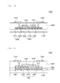
- FIGS. 1A to 1G are cross-sectional views of thin-film transistors according to various exemplary embodiments of the present invention.
- FIGS. 2A and 2B are cross-sectional views of thin-film transistors according to various exemplary embodiments of the present invention.
- FIG. 3A is a schematic diagram of a display device according to an exemplary embodiment of the present invention.
- FIG. 3B is a schematic diagram illustrating a sub-pixel region depicted in FIG. 3A .
- FIG. 4 is a flowchart describing a method for manufacturing a thin-film transistor according to an exemplary embodiment of the present invention.
- FIGS. 5A to 5E illustrate cross-sectional views of a TFT during the fabrication according to an exemplary method of manufacturing the thin-film transistor described in the present disclosure.
- An element or layer disposed or formed “on” another element or layer includes all a case in which an element is formed in direct physical contact with another element, as well as cases in which an element is indirectly physically connected with another element with one or more additional elements or layers formed therebetween.
- electrically connected refers to two different elements or layers that are in direct physical contact or are indirectly connected through one or more intervening elements or layers such that an electrical current is capable of flowing between the two different elements or layers.
- the inventors of the present invention have found that since the alignment among a gate electrode, a source electrode and a drain electrode are taken into account in a thin-film transistor having an inverted-staggered structure while preventing a short circuit between the source electrode and the drain electrode from occurring, there is a difficulty in short channel design in the thin-film transistor having an inverted-staggered structure. Furthermore, the inventors of the present invention have found that since a channel length depends on a width of a gate electrode in a thin-film transistor having a coplanar structure, it is difficult to minimize the channel length in terms of a design margin of the thin-film transistor. Accordingly, the inventors of the present invention have suggested a novel thin-film transistor structure and a method for manufacturing the same with which it is possible to reduce a channel length of the thin-film transistor while maintaining widths and an arrangement of the existing electrodes.
- FIG. 1A is a cross-section view of an exemplary thin-film transistor according to an embodiment of the present disclosure.
- a thin-film transistor 100 A includes a substrate 110 A, a conductive layer 140 A, an active layer 150 A, a gate insulating film 161 A, a gate electrode 120 A, an interlayer insulating film 162 A, a source electrode 131 A and a drain electrode 132 A.
- a thin-film transistor having a coplanar structure will be described.
- the substrate 110 A is a member for supporting various elements that can be formed on the substrate 110 A.
- the substrate 110 A may be made from an insulating material such as glass or plastic, but is not limited thereto.
- the substrate may be made from various materials.
- the substrate 110 A may be made from various materials depending on various applications in which the thin-film transistor 100 A is used.
- the substrate 110 A may be made from a flexible insulating material.
- examples of the available flexible insulating material include polyimide (PI), polyetherimide (PEI), polyethyelene terephthalate (PET), polycarbonate (PC), polystyrene (PS), styrene-acrylonitrile copolymer (SAN), and silicone-acrylic resin.
- the substrate 110 A may be made from a transparent insulating material.
- the conductive layer 140 A is formed on the substrate 110 A.
- the conductive layer 140 A is formed to reduce a channel region of the thin-film transistor 100 A, and may be made from a conductive metal material.
- the conductive layer 140 A may be made from the same material as that of the gate electrode 120 A to be described below, or may be made from the same material as those of the source electrode 131 A and the drain electrode 132 A.
- the conductive layer 140 A comes in contact with the active layer 150 A to be described below, is overlapped with at least a part of the gate electrode 120 A, and insulated from the gate electrode 120 A. Accordingly, the conductive layer 140 A can reduce a channel length of the thin-film transistor 100 A. For example, it is possible to reduce a current channel length of about 9 ⁇ m up to 4.5 ⁇ m by forming the conductive layer 140 A.
- the active layer 150 A is formed on the substrate 110 A.
- the active layer 150 A is also referred to as an activation layer, and may be a layer including an oxide semiconductor.
- Various metal oxides may be used as the oxide semiconductor of the active layer 150 A.
- examples of a constituent material of the oxide semiconductor includes a quaternary metal oxide such as an indium-tin-gallium-zinc-oxide (In—Sn—Ga—Zn—O)-based material, a ternary metal oxide such as an indium-gallium-zinc-oxide (In—Ga—Zn—O)-based material, an indium-tin-zinc-oxide (In—Sn—Zn—O)-based material, an indium-aluminum-zinc-oxide (In—Al—Zn—O)-based material, an indium-hafnium-zinc-oxide (In—Hf—Zn—O)-based material, a tin-gallium-zinc
- composition ratios of the elements included in the respective oxide semiconductor materials are not particularly limited, and may be adjusted at various composition ratios.
- the active layer 150 A may be formed by depositing the oxide semiconductor material on the substrate 110 A and then patterning the oxide semiconductor material so as to allow only the oxide semiconductor corresponding to a size of the active layer 150 A desired to be formed to be remained.
- the active layer 150 A includes a first region 151 A serving as a general oxide semiconductor region to which electrical conductivity has not been given (e.g., no addition of charge carriers through plasma treatment) and second regions 152 A serving as oxide semiconductor regions to which electrical conductivity has been given (e.g., addition of charge carriers through plasma treatment).
- the first region 151 A of the active layer 150 A is the part of the active layer 150 A being overlapped with the gate electrode 120 A.
- the second region 152 A of the active layer 150 A is the part of the active layer 150 A that is not overlapped by the gate electrode 120 A.
- the first region 151 A and second regions 152 A of the active layer are laterally next to each other, as they are both part of the active layer.
- electrical conductivity having been given to the oxide semiconductor does not necessarily mean that the oxide semiconductor has become a perfect conductor, but rather means that the oxide semiconductor has been treated to have properties to cause to it to act more like a conductor to another oxide semiconductor that has not been similarly modified.
- electrical conductivity having been given to the oxide semiconductor means that the oxide semiconductor has been treated to have a carrier concentration of 10 17 /m 3 or more.
- the second regions 152 A of the active layer 150 A are regions to which electrical conductivity has been given and have higher electrical conductivity than that of the first region 151 A of the active layer 150 A to which electrical conductivity has not been given. Thus, the second regions may be referred to as low-resistance regions.
- Some portions of the active layer 150 A are formed on the conductive layer 140 A to come in contact with the conductive layer 140 A. Specifically, a part of the first region 151 A and at least some portion of the second region 152 A of the active layer 150 A may be formed directly on the conductive layer 140 A.
- the gate insulating film 161 A is formed on the active layer 150 A.
- the gate insulating film 161 A insulates the active layer 150 A from the gate electrode 120 A.
- the gate insulating film 161 A may be a silicon oxide film, a silicon nitride film or multiple layers including the silicon oxide film and the silicon nitride film, but is not limited thereto.
- the gate insulating film may be made from various materials.
- the gate insulating film 161 A may be formed over the entire surface of the substrate 110 A including the active layer 150 A. However, since the gate insulating film 161 A has only to insulate the active layer 150 A from the gate electrode 120 A, the gate insulating film 161 A may be formed only on the active layer 150 A as shown in FIG.
- the gate insulating film 161 A may be formed so as to have contact holes for opening partial regions of the active layer 150 A, and the contact holes may open partial regions of the second region 152 A of the active layer 150 A.
- the gate electrode 120 A is formed on the gate insulating film 161 A.
- the gate electrode 120 A is overlapped with at least a part of the active layer 150 A, specifically, the first region 151 A of the active layer 150 A.
- the gate electrode 120 A may be formed to have the substantially same area as that of the gate insulating film 161 A.
- the gate electrode 120 A being formed to have the substantially same area as that of the gate insulating film 161 A includes a case where the areas of the gate electrode 120 A and the gate insulating film 161 A on a contact surface between the gate electrode 120 A and the gate insulating film 161 A are not completely the same due to a deviation in the process.
- the gate electrode 120 A is made from a conductive material, for example, molybdenum (Mo), aluminum (Al), chrome (Cr), gold (Au), titanium (Ti), nickel (Ni), neodymium (Nd) and copper (Cu), or an alloy thereof, but is not limited thereto.
- the gate electrode may be made from various materials.
- the gate electrode 120 A may be multiple layers made from any one selected from a group consisting of molybdenum (Mo), aluminum (Al), chrome (Cr), gold (Au), titanium (Ti), nickel (Ni), neodymium (Nd) and copper (Cu), or an alloy thereof.
- the gate insulating film 161 A and the gate electrode 120 A are formed only on the first region 151 A of the active layer 150 A.
- the first region 151 A of the active layer 150 A is the general oxide semiconductor region to which electrical conductivity has not been given
- the second regions 152 A of the active layer 150 A are the oxide semiconductor region to which electrical conductivity has been given.
- the gate insulating film 161 A and the gate electrode 120 A are formed on the first region 151 A of the active layer 150 A, and then hydrogen-plasma treatment or helium-plasma treatment is performed only on the second regions 152 A of the active layer 150 A by using the gate insulating film 161 A and the gate electrode 120 A as masks. In this way, it is possible to give electrical conductivity to only the second regions 152 A of the active layer 150 A.
- the interlayer insulating film 162 A is formed on the gate electrode 120 A.
- the interlayer insulating film 162 A may be made from the same material as that of the gate insulating film 161 A.
- the interlayer insulating film may be a silicon oxide film, a silicon nitride film or multiple layers including the silicon oxide film and the silicon nitride film, but is not limited thereto.
- the interlayer insulating film may be made from various materials.
- the interlayer insulating film 162 A may be formed over the entire surface of the substrate 110 A, and the source electrode 131 A and the drain electrode 132 A may be electrically connected to the active layer 150 A through contact holes of the interlayer insulating film 162 A.
- the source electrode 131 A and the drain electrode 132 A are formed on the interlayer insulating film 162 A.
- the source electrode 131 A and the drain electrode 132 A may contact the second regions 152 A of the active layer 150 A through the contact holes that are formed in the interlayer insulating film 162 A and/or the gate insulating film 161 A.
- the source electrode 131 A and the drain electrode 132 A are made from conductive materials.
- the source electrode 131 A and the drain electrode 132 A may be made from any one of, for example, molybdenum (Mo), aluminum (Al), chrome (Cr), gold (Au), titanium (Ti), nickel (Ni), neodymium (Nd) and copper (Cu), or an alloy thereof, but is not limited thereto.
- the source electrode and the drain electrode may be made from various materials. Further, the source electrode 131 A and the drain electrode 132 A may be multiple layers made from any one selected from a group consisting of molybdenum (Mo), aluminum (Al), chrome (Cr), gold (Au), titanium (Ti), nickel (Ni), neodymium (Nd) and copper (Cu), or an alloy thereof.
- Mo molybdenum
- Al aluminum
- Cr chrome
- Au gold
- Ti titanium
- Ni nickel
- Nd neodymium
- Cu copper
- the source electrode 131 A and the drain electrode 132 A each come in contact with one of the second regions 152 A of the active layer 150 A.
- the second region 152 A of the active layer 150 A in contact with the source electrode 131 A is separated, both electrically and physically, from the second region 152 A of the active layer 150 A in contact with the drain electrode 132 A.
- One of the second region 152 A of the active layer 150 A in contact with the source electrode 131 A and the second region 152 A of the active layer 150 A in contact with the drain electrode 132 A comes in contact with the conductive layer 140 A.
- the second region 152 A of the active layer 150 A in contact with the source electrode 131 A comes in contact with the conductive layer 140 A, but the present invention is not limited to such illustration.
- the second region 152 A of the active layer 150 A in contact with the drain electrode 132 A may come in contact with the conductive layer 140 A.
- the source electrode 131 A comes in contact with the second region 152 A of the active layer 150 A
- the second region 152 A of the active layer 150 A in contact with the source electrode 131 A comes in contact with the conductive layer 140 A.
- the conductive layer 140 A comes in contact with a partial region of the first region 151 A of the active layer 150 A, and the conductive layer 140 A is overlapped with at least a part of the gate electrode 120 A.
- the first region 151 A of the active layer 150 A may be formed between two separate second regions 152 A formed at the opposite ends of the active layer 150 A.
- One of the second regions 152 A may be electrically connected with the source electrode while the other second region 152 A may be electrically connected with the drain electrode.
- the conductive layer 140 A being overlapped with a part of the first region 151 A may overlap with any one of the second regions 152 A.
- the conductive layer 140 A may overlap with some part or entirety of the second region 152 A at the source electrode side.
- the conductive layer 140 A may overlap with some part or entirety of the second region 152 A at the drain electrode side.
- the thin-film transistor 100 A may employ two separate conductive layers, each configured to overlap with a part of the first region 151 A and at least some portion of one of the second regions 152 A, to further reduce the channel length of the thin-film transistor.
- the conductive layer 140 A which is made from a metal material and has a relatively higher carrier concentration other than the first region 151 A of the active layer 150 A which is overlapped with the conductive layer 140 A, is made from an oxide semiconductor, and has a relatively lower carrier concentration.
- the first region 151 A may be subdivided, for purposes of description only, into two portions.
- a first portion (not separately labeled) of the first region 151 A is the portion of the first region 151 A that is overlapped by the gate electrode 120 A and the gate insulating film (or layer) 161 A but not the conductive layer/s 140 A.
- the first portion of the first region 151 A is where the channel of the transistor will form when appropriate voltages are applied to the transistor.
- a second portion (also not separately labeled) of the first region 151 A is the portion of the first region 151 A that is overlapped by the gate electrode 120 A, the gate insulating film 161 A, and the conductive layer/s 140 A.
- the conductive layer 140 A serves as an extension of the source electrode 131 A, and thus the first portion of the first region 151 A of the active layer 150 A which does not overlap with the conductive layer 140 A becomes the channel region of the thin-film transistor.
- the channel length becomes the distance “L” shown in FIG. 1A , which is obtained by subtracting a length of the conductive layer 140 A overlapped with the gate electrode 120 A (e.g., the length of the second portion of the first region 151 A) from the entire width of the first region 151 A of the active layer 150 A.
- the channel length of the oxide semiconductor thin-film transistor can be reduced to the length between an end of the first conductive layer and an end of the second conductive layer that face each other (e.g., the length of the first portion of the first region 151 A).
- the distance between the conductive layer 140 A and overlapping source/drain electrodes can be configured such that capacitance is formed therebetween.
- This additional capacitance increases the total capacitance between the source electrode and the gate electrode and/or between the drain electrode and the gate electrode. Accordingly, it is possible to improve driving characteristics of the thin-film transistor.
- FIG. 1B is a cross-sectional view of a thin-film transistor according to an exemplary embodiment of the present invention.
- the conductive layer 140 B comes in direct contact with one of a source electrode 131 B and a drain electrode 132 B, and the other electrode, which is not in direct contact with the conductive layer 140 B, is in contact with the second region 152 B of the active layer 150 B.
- the conductive layer 140 B serves as the extension of the source electrode 131 B, it is possible to reduce a length of the channel region by a length of the conductive layer 140 B overlapped with the gate electrode 120 B as compared with a case where the conductive layer 140 B is not used.
- the source electrode 131 B comes in direct contact with the conductive layer 140 B made from a conductive metal material, it is possible to reduce a contact resistance between the source electrode 131 B and the conductive layer 140 B and a resistance between the source electrode 131 B and the channel region.
- the source electrode 131 B comes in contact with the conductive layer 140 B and the drain electrode 132 B comes in contact with the second region 152 B of the active layer 150 B, but the present invention is not limited to such illustration.
- the drain electrode 132 B may come in contact with the conductive layer 140 B, and the source electrode 131 B may come in contact with the second region 152 B of the active layer 150 B.
- a conductive layer 140 C may be formed on a top surface of an active layer 150 C as shown in FIG. 1C .
- a region of second regions 152 D of an active layer 150 D in contact with a source electrode 131 D may be formed only on a partial region of a conductive layer 140 D, and the source electrode 131 D may come in contact with one end surface of the second region 152 D of the active layer 150 D and a top surface of the conductive layer 140 D.
- FIG. 1E is a cross-sectional view of a thin-film transistor according to an exemplary embodiment of the present invention.
- the conductive layer ( 140 A, 140 B, 140 C, 140 D) is formed only at one end of the active layer ( 150 A, 150 B, 150 C, 150 D). In the some embodiments, however, the conductive layer 140 E may be formed at both ends of an active layer 150 E to be separated from each other, as illustrated in FIG. 1E . By doing this, it is possible to reduce a length of the channel region. For example, as shown in FIG. 1E , a first conductive layer 141 E of the conductive layer 140 E is formed below a source electrode 131 E, and a second conductive layer 142 E of the conductive layer 140 E is formed below a drain electrode 132 E.
- the source electrode 131 E and the drain electrode 132 E may be formed so as to come in direct contact with the first conductive layer 141 E and the second conductive layer 142 E without interposing the active layer 150 E, similarly to the embodiment 100 B illustrated in FIG. 1B .
- the embodiment 100 C of FIG. 1C regarding the relative order of stacking of the conductive and active layers
- the embodiment 100 D of FIG. 1D regarding the lateral extent of the active layer with respect to the electrode and conductive layer.
- FIG. 1F is a cross-sectional view of a thin-film transistor according to an exemplary embodiment of the present invention.
- a light blocking layer 181 F is further formed between a substrate 110 F and an active layer 150 F. Accordingly, the light blocking layer 181 F is formed to prevent light entering from below the substrate 110 F from reaching the active layer 150 F.
- the light blocking layer 181 F made from a reflective metal material is insulated from the active layer 150 F and a conductive layer 140 F by a buffer layer 180 F which is formed on the substrate 110 F and is made from an insulating material. As shown in FIG. 1F , when the conductive layer 140 F is formed under the active layer 150 F, the light blocking layer 181 F and the conductive layer 140 F can prevent light entering from below the substrate 110 F from reaching the active layer 150 F.
- the buffer layer 180 F functions to electrically insulate the light blocking layer 181 F from the active layer 150 F and the conductive layer 140 F and may also function to prevent water or other impurities from infiltrating through the substrate 110 F.
- a material constituting the buffer layer 180 F may be selected depending on the functions of the buffering layer 180 F, a type of the thin-film transistor, a constituent material of the thin-film transistor 100 F in contact with the buffer layer 180 F, and structural characteristics thereof.
- the buffer layer 180 F may be selected depending on interface characteristics with the active layer 150 F according to the structure of the thin-film transistor 100 F.
- the buffer layer may be a silicon oxide film, a silicon nitride film, or multiple layers including the silicon oxide film and the silicon nitride film.
- the buffer layer 180 F may be formed of a plurality of layers with different refractive indices for scattering external light entering from the outside.
- FIG. 1G is a cross-sectional view of a thin-film transistor according to an exemplary embodiment of the present invention.
- a light scattering pattern 145 G is formed on a substrate 110 G.
- the light scattering pattern 145 G may be made from a reflective metal material.
- the light scattering pattern 145 G may be made from the substantially same material as that of a conductive layer 140 G and may be simultaneously formed with the conductive layer.
- the light scattering pattern 145 G may be formed by forming a reflective metal material on the substrate 110 G and removing the reflective metal material in regions except for regions corresponding to the conductive layer 140 G and the light scattering pattern 145 G.
- the light scattering pattern 145 G is formed to minimize light reaching the active layer 150 G by scattering the light entering the active layer 150 G.
- the light scattering pattern 145 G may be formed close to a side surface of the active layer 150 G on the substrate 110 G. Specifically, the light scattering pattern 145 G can scatter the entering light at the side surface of the active layer 150 G to change a path of the light entering toward the active layer 150 G. Accordingly, by minimizing the amount of the light that has reached the active layer 150 G, it is possible to minimize deterioration in reliability of the thin-film transistor 100 G due to the light.
- the light scattering pattern 145 G is maintained in a floating state so as not to electrically affect the thin-film transistor.
- one light scattering pattern 145 G is formed, a plurality of light scattering patterns may be formed to be separated from each other within an allowed space if necessary. Further, by using the light scattering pattern 145 G and a light blocking layer formed below the active layer 150 G, it is possible to minimize deterioration in reliability of the thin-film transistor 100 G due to the light entering the active layer 150 G.
- FIGS. 1F and 1G may also be combined with the embodiments of any of FIGS. 1A-1E as the light blocking and light reflecting layers of FIGS. 1F and 1G do not affect the constructions of those other embodiments.
- FIG. 2A is a cross-sectional view of a thin-film transistor according to an exemplary embodiment of the present invention.
- a thin-film transistor 200 A includes a substrate 210 A, a gate electrode 220 A, a gate insulating film 261 A, a conductive layer 240 A, an active layer 250 A, an etch stopper 270 A, a source electrode 231 A, and a drain electrode 232 A.
- a thin-film transistor having an inverted-staggered structure will be explained.
- the gate electrode 220 A is formed on the substrate 210 A.
- the gate insulating film 261 A is formed on the gate electrode 220 A.
- the gate insulating film 261 A insulates the active layer 250 A from the gate electrode 220 A. Since the gate insulating film 261 A need to insulate the active layer 250 A from the gate electrode 220 A, the gate insulating film 261 A may be formed to cover the gate electrode 220 A on the gate electrode 220 A. For example, as shown in FIG. 2A , the gate insulating film 261 A may be formed over the entire surface of the substrate 210 A to cover the gate electrode 220 A.
- the conductive layer 240 A is formed on the gate insulating film 261 A so as to be overlapped with the gate electrode 220 A.
- the conductive layer 240 A is formed to reduce a channel region of the thin-film transistor 200 A, and may be made from a conductive metal material.
- the active layer 250 A is formed on the gate insulating film 261 A and the conductive layer 240 A.
- the active layer 250 A may be formed to cover at least a part of the conductive layer 240 A.
- the conductive layer 240 A comes in contact with the active layer 250 A, and is insulated from the gate electrode 220 A.
- the etch stopper 270 A is formed on the active layer 250 A, and the source electrode 231 A and the drain electrode 232 A are formed on the active layer 250 A and the etch stopper 270 A.
- the source electrode 231 A and the drain electrode 232 A may come in contact with the active layer 250 A to be electrically connected to the active layer 250 A, and may be formed on a partial region of the etch stopper 270 A.
- the active layer 250 A including the oxide semiconductor may be damaged during an etching process on the source electrode 231 A and the drain electrode 232 A that are positioned on the active layer 250 A.
- the etch stopper 270 A made from an insulating material is formed on the active layer 250 A, specifically, in a space between the source electrode 231 A and the drain electrode 232 A.
- the substrate 210 A, the active layer 250 A, the gate insulating film 261 A, the gate electrode 220 A, the source electrode 231 A and the drain electrode 232 A may be made from the same materials as those of the substrate 110 A, the active layer 150 A, the gate insulating film 161 A, the gate electrode 120 A, the source electrode 131 A and the drain electrode 132 A shown in FIG. 1A and may have the same configurations as those thereof.
- the shortest distance between a contact point of the source electrode 231 A with the active layer 250 A and a contact point of the drain electrode 232 A with the active layer 250 A forms the channel region.
- the conductive layer 240 A being interposed between the active layer 250 A and the gate insulating film 261 A is overlapped with the part of the active layer 250 A defined by the etch stopper 270 A.
- the conductive layer 240 A is made from a metal material and has a relatively higher carrier concentration than the portion of active layer 250 A that it overlaps,
- the active layer 250 A is made from an oxide semiconductor, and has a relatively low carrier concentration compared to the conductive layer 240 A.
- a substantial channel length becomes a distance obtained by subtracting a length of the conductive layer 240 A overlapped with the active layer 250 A from a distance between the contact point of the source electrode 231 A with the active layer 250 A and the contact point of the drain electrode 232 A with the active layer 250 A. That is, since the channel length is a sum of a distance L 1 between a portion of the active layer 250 A in contact with the source electrode 231 A and one end of the conductive layer 240 A and a distance L 2 between a portion of the active layer 250 A in contact with the drain electrode 232 A and the other end of the conductive layer 240 A, it is possible to reduce a length of the channel by a length of the conductive layer 240 A.
- a conductive layer 240 B is formed so as to be overlapped with at least partial regions of a gate electrode 220 B and an etch stopper 270 B, and an active layer 250 B is formed to cover a partial region of a conductive layer 240 B.
- the shortest distance between a contact point of the source electrode 231 B with the active layer 250 B and a contact point of the drain electrode 232 B with the active layer 250 B may be defined as a distance of the channel region.
- a substantial distance of the channel region becomes a distance by subtracting a distance of the conductive layer 240 B overlapped with the active layer 250 B from the existing channel region, namely, a distance of a channel region 295 B.
- FIG. 3A is a conceptual diagram of a display device according to an exemplary embodiment of the present invention.
- FIG. 3B is an enlarged conceptual diagram of a sub-pixel region shown in FIG. 3A .
- a display device 300 is a display device to which the thin-film transistors according to various exemplary embodiments of the present invention are applicable.
- the display device 300 is a device for displaying an image, and examples of the display device include various displayer devices, such as an organic light-emitting diode (OLED) device, a liquid crystal display (LCD) device, and an electrophoretic display (EPD) device.
- OLED organic light-emitting diode
- LCD liquid crystal display
- EPD electrophoretic display
- the display device 300 includes a substrate 310 , at least one thin-film transistor, and an organic light-emitting diode (OLED) including an anode, an organic light-emitting layer and a cathode.
- At least one thin-film transistor for emitting the organic light-emitting layer is included in a plurality of sub-pixel regions SP of the substrate 310 of the display device 300 .
- two thin-film transistors of a switching transistor TR 1 and a driving transistor TR 2 may be included in the sub-pixel region SP, but the number of transistors is not limited thereto.
- Various thin-film transistors for a variety purposes may be further included in the sub-pixel region.
- the switching transistor TR 1 includes a gate electrode connected to a gate wiring S extending from a gate driving module 320 , a first electrode connected to a data wiring D extending from a data driving module 330 , and a second electrode connected to a gate electrode of the driving transistor TR 2 .
- the first electrode and the second electrode of the switching transistor TR 1 are a source electrode and a drain electrode, respectively, and the first electrode and the second electrode may be determined as one of the source electrode and the drain electrode depending on a kind of the switching transistor TR 1 .
- the driving transistor TR 2 includes the gate electrode connected to the second electrode of the switching transistor TR 1 , a first electrode connected to a first power supply wiring Vdd extending from a power supply module 340 , and a second electrode connected to the organic light-emitting diode (OLED).
- the first electrode and the second electrode of the driving transistor TR 2 are a source electrode and a drain electrode, respectively and the first electrode and the second electrode may be determined as one of the source electrode and the drain electrode depending on a kind of the driving transistor TR 2 .
- a first capacitor Cst is formed between the gate electrode of the driving transistor TR 2 and the second electrode of the driving transistor TR 2 , and as a value of the first capacitor Cst increases, a voltage transmission rate of a data voltage increases.
- the use of two thin-film transistors is effective.
- the thin-film transistors according to various exemplary embodiments of the present invention are applied to the driving transistor TR 2 of the display device 300 , that is, when the conductive layer which comes in contact with the active layer, is overlapped with at least a part of the gate electrode, and is insulated from the gate electrode is applied to the driving transistor TR 2 , since the conductive layer is overlapped with at least a part of the gate electrode, a second capacitor Cp is formed between the gate electrode and the conductive layer. Furthermore, when a region of the active layer in contact with the conductive layer comes in contact with the second electrode of the driving transistor TR 2 , the second capacitor Cp has a value different from that of the first capacitor Cst.
- the second capacitor is connected to the first capacitor Cst in parallel, a total capacitor value of the gate electrode of the driving transistor TR 2 and the second electrode of the driving transistor TR 2 increases. Accordingly, when the thin-film transistors according to various exemplary embodiments of the present invention are applied to the driving transistor TR 2 of the display device 300 , since a capacitor value between the gate electrode of the driving transistor TR 2 and the second electrode of the driving transistor TR 2 increases, it is advantageous to a voltage transmission rate of a data voltage.
- each of the plurality of sub-pixel regions SP of the organic light-emitting diode display device includes a light-emitting region and a light-transmitting region, and the thin-film transistor and the organic light-emitting diode may be arranged in the organic light-emitting region.
- a design of the thin-film transistor may be partially changed depending on a kind of the display device 300 .
- the display device 300 is a flexible display device, since the display device 300 needs to be repeatedly bent or folded, various elements constituting the thin-film transistor need to be easily bent or folded.
- the display device 300 is a transparent display device, even though the display device 300 is viewed from one side, the other side of the display device needs to be viewed to some extent. Accordingly, the various elements constituting the thin-film transistor may be considerably decreased in size, or may be made from transparent materials.
- the display device may be a liquid crystal display device, and the liquid crystal display device includes a lower substrate, an upper substrate, a pixel electrode, a common electrode, a color filter and a liquid crystal layer interposed between the upper substrate and the lower substrate.
- the liquid crystal display device includes a plurality of pixel regions, and includes a plurality of thin-film transistors for individually driving the plurality of pixel regions.
- the conductive layer may be formed below the drain electrode of the thin-film transistor.
- the conductive layer may be formed below the drain electrode of the thin-film transistor so as to allow the capacitor formed between the conductive layer and the gate electrode to function as a storage capacitor.
- FIG. 4 is a flowchart for describing a method for manufacturing a thin-film transistor according to an exemplary embodiment of the present invention.
- FIGS. 5A to 5E are cross-sectional views of processes for describing the method for manufacturing a thin-film transistor according to the exemplary embodiment of the present invention.
- a conductive layer is formed on a substrate (S 40 ).
- a process of forming the conductive layer will be described in detail with reference to FIG. 5A .
- a conductive layer 540 is formed on a substrate 510 .
- the forming of the conducting layer 540 may include forming a metal material for a conductive layer on the entire surface of the substrate 510 and selectively patterning the metal material for a conductive layer by a photolithography process.
- a light scattering pattern 545 may be formed simultaneously with the conductive layer 540 and may be made from the same material as that of the conductive layer 540 .
- the forming of the light scattering pattern 545 may include forming the light scattering pattern 545 simultaneously with the conductive layer 540 by forming the metal material for a conductive layer on the entire surface of the substrate 510 and selectively patterning the metal material for a conductive layer by a photolithography process.
- an active layer in contact with the conductive layer is formed on at least a part of the conductive layer (S 41 ), a gate insulating film is formed on the active layer (S 42 ), and then a gate electrode is formed on the gate insulating film (S 43 ).
- an active layer 550 in contact with the conductive layer 540 is formed on at a least a partial region of the conductive layer 540 .
- the forming of the active layer 550 may include forming the active layer 550 by forming a semiconductor, which is a material for an active layer on the entire surface of the substrate 510 including the conductive layer 540 and selectively patterning the material for an active layer by a photolithography process. Although it has been illustrated in FIG. 5C that the active layer 550 is formed on the entire region of the conductive layer 540 , the present invention is not limited thereto.
- the active layer 550 may be formed on a partial region of the conductive layer 540 .
- a gate insulating film 561 and a gate electrode 520 are formed on a partial region of the active layer 550 after forming the active layer 550 .
- the forming of the gate insulating film 561 and the gate electrode 520 may include forming a material for a gate insulating film and a material for a gate electrode over the entire surface of the substrate 510 and selectively patterning the material for a gate insulating film and the material for a gate electrode by a photolithography process.
- electrical conductivity may be given to a partial region of the active layer 550 .
- the giving of the electrical conductivity to the partial region of the active layer 550 may include giving electrical conductivity to a partial region of the active layer 550 by using the gate electrode 520 as a mask.
- the giving of the electrical conductivity to the partial region of the active layer 550 is to reduce resistances of regions of the active layer 550 in contact with a source electrode 531 and a drain electrode 532 . While electrical conductivity is not given to a first region 551 of the active layer 550 overlapped with the gate electrode 520 by using the gate electrode 520 as a mask, electrical conductivity may be given to only second regions 552 of the active layer 550 that are overlapped with the source electrode and the drain electrode.
- an interlayer insulating film is formed on the gate electrode (S 44 ), and a source electrode and a drain electrode that are electrically connected to the active layer are formed (S 45 ).
- the forming of an interlayer insulating film 562 may include forming contact holes for opening the second regions 552 of the active layer 550 by forming a material for an interlayer insulating film over the entire surface of the substrate 510 on which the gate electrode 520 is formed and selectively patterning the material for an interlayer insulating film by a photolithography process.
- the source electrode 531 and the drain electrode 532 that are electrically connected to the active layer 550 may be formed after forming the interlayer insulating film 562 including the contact holes.
Landscapes
- Physics & Mathematics (AREA)
- Engineering & Computer Science (AREA)
- Nonlinear Science (AREA)
- Microelectronics & Electronic Packaging (AREA)
- Crystallography & Structural Chemistry (AREA)
- Chemical & Material Sciences (AREA)
- Mathematical Physics (AREA)
- Power Engineering (AREA)
- General Physics & Mathematics (AREA)
- Optics & Photonics (AREA)
- Geometry (AREA)
- Thin Film Transistor (AREA)
- Electroluminescent Light Sources (AREA)
Applications Claiming Priority (2)
| Application Number | Priority Date | Filing Date | Title |
|---|---|---|---|
| KR1020130034429A KR102178766B1 (ko) | 2013-03-29 | 2013-03-29 | 박막 트랜지스터, 박막 트랜지스터 제조 방법 및 박막 트랜지스터를 포함하는 표시 장치 |
| KR10-2013-0034429 | 2013-03-29 |
Publications (2)
| Publication Number | Publication Date |
|---|---|
| US20140291635A1 US20140291635A1 (en) | 2014-10-02 |
| US9240486B2 true US9240486B2 (en) | 2016-01-19 |
Family
ID=51619915
Family Applications (1)
| Application Number | Title | Priority Date | Filing Date |
|---|---|---|---|
| US14/095,278 Active US9240486B2 (en) | 2013-03-29 | 2013-12-03 | Thin-film transistor, method for manufacturing the same and display device including the same |
Country Status (5)
| Country | Link |
|---|---|
| US (1) | US9240486B2 (de) |
| EP (2) | EP3242328B1 (de) |
| KR (1) | KR102178766B1 (de) |
| CN (1) | CN105308752B (de) |
| WO (1) | WO2014157814A1 (de) |
Cited By (2)
| Publication number | Priority date | Publication date | Assignee | Title |
|---|---|---|---|---|
| US20160118383A1 (en) * | 2011-03-04 | 2016-04-28 | Semiconductor Energy Laboratory Co., Ltd. | Semiconductor device |
| US20160225837A1 (en) * | 2015-02-04 | 2016-08-04 | Samsung Display Co., Ltd. | Semiconductor element and organic light emitting display device having a semiconductor element |
Families Citing this family (26)
| Publication number | Priority date | Publication date | Assignee | Title |
|---|---|---|---|---|
| EP2963687B1 (de) * | 2014-07-03 | 2020-03-18 | LG Display Co., Ltd. | Organisches elektrolumineszenzelement |
| KR102346675B1 (ko) * | 2014-10-31 | 2022-01-04 | 삼성디스플레이 주식회사 | 디스플레이 장치 및 그 제조 방법 |
| CN105023951B (zh) * | 2015-07-10 | 2019-08-13 | 广州奥翼电子科技股份有限公司 | 半导体薄膜晶体管及其制造方法以及显示装置及其背板 |
| KR102789164B1 (ko) * | 2015-12-29 | 2025-03-28 | 가부시키가이샤 한도오따이 에네루기 켄큐쇼 | 금속 산화물막 및 반도체 장치 |
| KR102509088B1 (ko) * | 2016-03-14 | 2023-03-10 | 삼성디스플레이 주식회사 | 표시 장치 |
| KR102508743B1 (ko) * | 2016-07-19 | 2023-03-14 | 삼성디스플레이 주식회사 | 유기전계발광 표시장치의 구동 드라이버 |
| CN106024781B (zh) * | 2016-07-22 | 2019-06-04 | 京东方科技集团股份有限公司 | 静电放电器件、其制造方法及阵列基板、显示面板和装置 |
| CN107664889B (zh) * | 2017-09-14 | 2020-05-22 | 深圳市华星光电半导体显示技术有限公司 | 一种tft器件及液晶显示面板的静电保护电路 |
| CN107706306B (zh) * | 2017-10-26 | 2020-02-04 | 京东方科技集团股份有限公司 | 一种有机发光二极管显示基板及其制作方法、显示装置 |
| JP2019091794A (ja) * | 2017-11-14 | 2019-06-13 | シャープ株式会社 | 半導体装置 |
| KR20190072201A (ko) * | 2017-12-15 | 2019-06-25 | 엘지디스플레이 주식회사 | 슬로프 액티브층을 포함하는 표시패널 및 이를 제조하는 방법 |
| CN109037346B (zh) * | 2018-07-27 | 2020-06-02 | 京东方科技集团股份有限公司 | 薄膜晶体管、显示基板及其制作方法、显示装置 |
| KR102603688B1 (ko) * | 2018-11-28 | 2023-11-17 | 엘지디스플레이 주식회사 | 수직 구조 트랜지스터 및 전자장치 |
| KR102486147B1 (ko) * | 2018-12-18 | 2023-01-10 | 엘지디스플레이 주식회사 | 박막 트랜지스터 어레이 기판 및 이를 포함하는 전자장치 |
| GB2587793B (en) | 2019-08-21 | 2023-03-22 | Pragmatic Printing Ltd | Electronic circuit comprising transistor and resistor |
| GB2610886B (en) * | 2019-08-21 | 2023-09-13 | Pragmatic Printing Ltd | Resistor geometry |
| CN111029342B (zh) * | 2019-11-07 | 2024-04-16 | 深圳市华星光电半导体显示技术有限公司 | 显示面板及其制备方法、显示装置 |
| KR102625951B1 (ko) * | 2019-12-23 | 2024-01-16 | 엘지디스플레이 주식회사 | 박막 트랜지스터 어레이 기판 및 이를 포함하는 전자장치 |
| CN113327989B (zh) * | 2021-05-19 | 2022-05-17 | 厦门天马微电子有限公司 | 薄膜晶体管、阵列基板、显示面板及显示装置 |
| CN113437156A (zh) * | 2021-06-07 | 2021-09-24 | 惠州华星光电显示有限公司 | 半导体器件及其制备方法 |
| KR102910273B1 (ko) * | 2021-10-12 | 2026-01-08 | 엘지디스플레이 주식회사 | 박막 트랜지스터, 그 제조방법 및 이를 포함하는 표시장치 |
| KR102864036B1 (ko) * | 2021-10-29 | 2025-09-23 | 엘지디스플레이 주식회사 | 박막 트랜지스터 및 이를 포함하는 표시장치 |
| CN114883343B (zh) * | 2022-04-21 | 2024-03-26 | 北海惠科光电技术有限公司 | 薄膜晶体管、显示基板和薄膜晶体管的制备方法 |
| CN115101590B (zh) * | 2022-06-24 | 2026-02-13 | 京东方科技集团股份有限公司 | 一种晶体管、其制作方法及驱动基板 |
| CN115377191B (zh) * | 2022-08-10 | 2025-11-21 | 武汉华星光电技术有限公司 | 薄膜晶体管及电子器件 |
| CN115377202A (zh) * | 2022-10-25 | 2022-11-22 | Tcl华星光电技术有限公司 | 显示面板及其制作方法、显示装置 |
Citations (8)
| Publication number | Priority date | Publication date | Assignee | Title |
|---|---|---|---|---|
| JP2008146091A (ja) | 2008-01-11 | 2008-06-26 | Sony Corp | 画素回路及びその駆動方法 |
| US20090256203A1 (en) | 2008-04-14 | 2009-10-15 | Hidayat Kisdarjono | Top Gate Thin Film Transistor with Independent Field Control for Off-Current Suppression |
| US20090321732A1 (en) | 2008-06-30 | 2009-12-31 | Samsung Mobile Display Co., Ltd. | Thin film transistor, method of manufacturing the same and flat panel display device having the same |
| US20120088339A1 (en) | 2010-10-12 | 2012-04-12 | Io Semiconductor, Inc. | Vertical Semiconductor Device with Thinned Substrate |
| KR20120053768A (ko) | 2010-11-18 | 2012-05-29 | 엘지디스플레이 주식회사 | 유기전계발광표시장치 및 그 제조방법 |
| US20120175615A1 (en) * | 2011-01-10 | 2012-07-12 | Samsung Mobile Display Co., Ltd. | Organic Light-Emitting Display and Method of Manufacturing the Same |
| US20120223304A1 (en) * | 2011-03-04 | 2012-09-06 | Semiconductor Energy Laboratory Co., Ltd. | Semiconductor device |
| US20130256652A1 (en) * | 2012-04-02 | 2013-10-03 | Yong Su LEE | Thin film transistor, thin film transistor array panel including the same, and method of manufacturing the same |
Family Cites Families (10)
| Publication number | Priority date | Publication date | Assignee | Title |
|---|---|---|---|---|
| JPH06268220A (ja) * | 1993-03-17 | 1994-09-22 | Fujitsu Ltd | 薄膜トランジスタ |
| JP3267271B2 (ja) * | 1998-12-10 | 2002-03-18 | 日本電気株式会社 | 液晶表示装置およびその製造法 |
| KR100480333B1 (ko) * | 2002-04-08 | 2005-04-06 | 엘지.필립스 엘시디 주식회사 | 액정표시장치용 어레이기판과 그 제조방법 |
| KR100884541B1 (ko) * | 2002-12-10 | 2009-02-18 | 엘지디스플레이 주식회사 | 액정표시장치 및 그 제조방법 |
| US7211825B2 (en) * | 2004-06-14 | 2007-05-01 | Yi-Chi Shih | Indium oxide-based thin film transistors and circuits |
| KR101250236B1 (ko) * | 2006-06-14 | 2013-04-05 | 엘지디스플레이 주식회사 | 칼라필터기판 및 이를 포함하는 액정표시소자의 제조방법 |
| JP5116277B2 (ja) * | 2006-09-29 | 2013-01-09 | 株式会社半導体エネルギー研究所 | 半導体装置、表示装置、液晶表示装置、表示モジュール及び電子機器 |
| US7879678B2 (en) * | 2008-02-28 | 2011-02-01 | Versatilis Llc | Methods of enhancing performance of field-effect transistors and field-effect transistors made thereby |
| EP2172977A1 (de) * | 2008-10-03 | 2010-04-07 | Semiconductor Energy Laboratory Co., Ltd. | Anzeigevorrichtung |
| KR101623961B1 (ko) * | 2009-12-02 | 2016-05-26 | 삼성전자주식회사 | 트랜지스터와 그 제조방법 및 트랜지스터를 포함하는 전자소자 |
-
2013
- 2013-03-29 KR KR1020130034429A patent/KR102178766B1/ko active Active
- 2013-12-03 US US14/095,278 patent/US9240486B2/en active Active
- 2013-12-27 EP EP17176806.2A patent/EP3242328B1/de active Active
- 2013-12-27 EP EP13880081.8A patent/EP2979302B1/de active Active
- 2013-12-27 CN CN201380070130.6A patent/CN105308752B/zh active Active
- 2013-12-27 WO PCT/KR2013/012245 patent/WO2014157814A1/en not_active Ceased
Patent Citations (10)
| Publication number | Priority date | Publication date | Assignee | Title |
|---|---|---|---|---|
| JP2008146091A (ja) | 2008-01-11 | 2008-06-26 | Sony Corp | 画素回路及びその駆動方法 |
| US20090256203A1 (en) | 2008-04-14 | 2009-10-15 | Hidayat Kisdarjono | Top Gate Thin Film Transistor with Independent Field Control for Off-Current Suppression |
| US20090321732A1 (en) | 2008-06-30 | 2009-12-31 | Samsung Mobile Display Co., Ltd. | Thin film transistor, method of manufacturing the same and flat panel display device having the same |
| US20120088339A1 (en) | 2010-10-12 | 2012-04-12 | Io Semiconductor, Inc. | Vertical Semiconductor Device with Thinned Substrate |
| KR20120053768A (ko) | 2010-11-18 | 2012-05-29 | 엘지디스플레이 주식회사 | 유기전계발광표시장치 및 그 제조방법 |
| US20120175615A1 (en) * | 2011-01-10 | 2012-07-12 | Samsung Mobile Display Co., Ltd. | Organic Light-Emitting Display and Method of Manufacturing the Same |
| US20120223304A1 (en) * | 2011-03-04 | 2012-09-06 | Semiconductor Energy Laboratory Co., Ltd. | Semiconductor device |
| US8659015B2 (en) * | 2011-03-04 | 2014-02-25 | Semiconductor Energy Laboratory Co., Ltd. | Semiconductor device |
| US20140117353A1 (en) * | 2011-03-04 | 2014-05-01 | Semiconductor Energy Laboratory Co., Ltd. | Semiconductor device |
| US20130256652A1 (en) * | 2012-04-02 | 2013-10-03 | Yong Su LEE | Thin film transistor, thin film transistor array panel including the same, and method of manufacturing the same |
Non-Patent Citations (1)
| Title |
|---|
| PCT International Search Report for PCT/KR2013/012245, Apr. 15, 2014, 3 Pages. |
Cited By (4)
| Publication number | Priority date | Publication date | Assignee | Title |
|---|---|---|---|---|
| US20160118383A1 (en) * | 2011-03-04 | 2016-04-28 | Semiconductor Energy Laboratory Co., Ltd. | Semiconductor device |
| US10032768B2 (en) * | 2011-03-04 | 2018-07-24 | Semiconductor Energy Laboratory Co., Ltd. | Semiconductor device |
| US20160225837A1 (en) * | 2015-02-04 | 2016-08-04 | Samsung Display Co., Ltd. | Semiconductor element and organic light emitting display device having a semiconductor element |
| US9748402B2 (en) * | 2015-02-04 | 2017-08-29 | Samsung Display Co., Ltd. | Semiconductor element and organic light emitting display device having a semiconductor element |
Also Published As
| Publication number | Publication date |
|---|---|
| WO2014157814A1 (en) | 2014-10-02 |
| US20140291635A1 (en) | 2014-10-02 |
| EP2979302A4 (de) | 2016-11-02 |
| KR102178766B1 (ko) | 2020-11-13 |
| CN105308752A (zh) | 2016-02-03 |
| EP3242328B1 (de) | 2020-10-28 |
| KR20140118462A (ko) | 2014-10-08 |
| EP3242328A1 (de) | 2017-11-08 |
| CN105308752B (zh) | 2018-07-27 |
| EP2979302A1 (de) | 2016-02-03 |
| EP2979302B1 (de) | 2020-12-16 |
Similar Documents
| Publication | Publication Date | Title |
|---|---|---|
| US9240486B2 (en) | Thin-film transistor, method for manufacturing the same and display device including the same | |
| US9837446B2 (en) | Thin film transistor array panel and manufacturing method thereof | |
| KR102137392B1 (ko) | 표시 장치 및 그 제조 방법 | |
| US8653515B2 (en) | Thin film transistor and thin film transistor array panel | |
| US9952473B2 (en) | Display panel including light shielding line, display device having the same and method of manufacturing the same | |
| CN103515395B (zh) | 显示装置及其制造方法 | |
| CN104851888B (zh) | 薄膜晶体管阵列面板 | |
| KR102380647B1 (ko) | 박막 트랜지스터 및 그 제조 방법 | |
| US20120112181A1 (en) | Oxide semiconductor, thin film transistor including the same and thin film transistor display panel including the same | |
| US8697535B2 (en) | Thin film transistor substrate and method for fabricating the same | |
| US10020324B2 (en) | Display device | |
| US20120126233A1 (en) | Thin film transistor array panel and method for manufacturing the same | |
| US20190266945A1 (en) | Display device | |
| US20150144951A1 (en) | Thin film transistor array panel and manufacturing method thereof | |
| KR20160130877A (ko) | 박막트랜지스터 및 이를 포함하는 표시 장치 | |
| US20170104017A1 (en) | Thin film transistor array substrate and method of manufacturing the same | |
| US9373683B2 (en) | Thin film transistor | |
| US10409126B2 (en) | Thin film transistor unaffected by light and display apparatus having the same | |
| KR102412069B1 (ko) | 박막 트랜지스터 | |
| US9613860B2 (en) | Method of manufacturing thin-film transistor |
Legal Events
| Date | Code | Title | Description |
|---|---|---|---|
| AS | Assignment |
Owner name: LG DISPLAY CO., LTD., KOREA, REPUBLIC OF Free format text: ASSIGNMENT OF ASSIGNORS INTEREST;ASSIGNOR:CHO, HYUNGNYUCK;REEL/FRAME:031726/0105 Effective date: 20131127 |
|
| STCF | Information on status: patent grant |
Free format text: PATENTED CASE |
|
| MAFP | Maintenance fee payment |
Free format text: PAYMENT OF MAINTENANCE FEE, 4TH YEAR, LARGE ENTITY (ORIGINAL EVENT CODE: M1551); ENTITY STATUS OF PATENT OWNER: LARGE ENTITY Year of fee payment: 4 |
|
| MAFP | Maintenance fee payment |
Free format text: PAYMENT OF MAINTENANCE FEE, 8TH YEAR, LARGE ENTITY (ORIGINAL EVENT CODE: M1552); ENTITY STATUS OF PATENT OWNER: LARGE ENTITY Year of fee payment: 8 |