US9235085B2 - Liquid crystal display device - Google Patents
Liquid crystal display device Download PDFInfo
- Publication number
- US9235085B2 US9235085B2 US13/723,549 US201213723549A US9235085B2 US 9235085 B2 US9235085 B2 US 9235085B2 US 201213723549 A US201213723549 A US 201213723549A US 9235085 B2 US9235085 B2 US 9235085B2
- Authority
- US
- United States
- Prior art keywords
- seal pattern
- line
- gate
- layer
- substrate
- Prior art date
- Legal status (The legal status is an assumption and is not a legal conclusion. Google has not performed a legal analysis and makes no representation as to the accuracy of the status listed.)
- Active, expires
Links
Images


Classifications
-
- G—PHYSICS
- G02—OPTICS
- G02F—OPTICAL DEVICES OR ARRANGEMENTS FOR THE CONTROL OF LIGHT BY MODIFICATION OF THE OPTICAL PROPERTIES OF THE MEDIA OF THE ELEMENTS INVOLVED THEREIN; NON-LINEAR OPTICS; FREQUENCY-CHANGING OF LIGHT; OPTICAL LOGIC ELEMENTS; OPTICAL ANALOGUE/DIGITAL CONVERTERS
- G02F1/00—Devices or arrangements for the control of the intensity, colour, phase, polarisation or direction of light arriving from an independent light source, e.g. switching, gating or modulating; Non-linear optics
- G02F1/01—Devices or arrangements for the control of the intensity, colour, phase, polarisation or direction of light arriving from an independent light source, e.g. switching, gating or modulating; Non-linear optics for the control of the intensity, phase, polarisation or colour
- G02F1/13—Devices or arrangements for the control of the intensity, colour, phase, polarisation or direction of light arriving from an independent light source, e.g. switching, gating or modulating; Non-linear optics for the control of the intensity, phase, polarisation or colour based on liquid crystals, e.g. single liquid crystal display cells
- G02F1/133—Constructional arrangements; Operation of liquid crystal cells; Circuit arrangements
- G02F1/1333—Constructional arrangements; Manufacturing methods
- G02F1/1339—Gaskets; Spacers; Sealing of cells
-
- G—PHYSICS
- G02—OPTICS
- G02F—OPTICAL DEVICES OR ARRANGEMENTS FOR THE CONTROL OF LIGHT BY MODIFICATION OF THE OPTICAL PROPERTIES OF THE MEDIA OF THE ELEMENTS INVOLVED THEREIN; NON-LINEAR OPTICS; FREQUENCY-CHANGING OF LIGHT; OPTICAL LOGIC ELEMENTS; OPTICAL ANALOGUE/DIGITAL CONVERTERS
- G02F1/00—Devices or arrangements for the control of the intensity, colour, phase, polarisation or direction of light arriving from an independent light source, e.g. switching, gating or modulating; Non-linear optics
- G02F1/01—Devices or arrangements for the control of the intensity, colour, phase, polarisation or direction of light arriving from an independent light source, e.g. switching, gating or modulating; Non-linear optics for the control of the intensity, phase, polarisation or colour
- G02F1/13—Devices or arrangements for the control of the intensity, colour, phase, polarisation or direction of light arriving from an independent light source, e.g. switching, gating or modulating; Non-linear optics for the control of the intensity, phase, polarisation or colour based on liquid crystals, e.g. single liquid crystal display cells
- G02F1/133—Constructional arrangements; Operation of liquid crystal cells; Circuit arrangements
- G02F1/1333—Constructional arrangements; Manufacturing methods
- G02F1/133354—Arrangements for aligning or assembling substrates
-
- G02F2001/133354—
-
- G—PHYSICS
- G02—OPTICS
- G02F—OPTICAL DEVICES OR ARRANGEMENTS FOR THE CONTROL OF LIGHT BY MODIFICATION OF THE OPTICAL PROPERTIES OF THE MEDIA OF THE ELEMENTS INVOLVED THEREIN; NON-LINEAR OPTICS; FREQUENCY-CHANGING OF LIGHT; OPTICAL LOGIC ELEMENTS; OPTICAL ANALOGUE/DIGITAL CONVERTERS
- G02F2202/00—Materials and properties
- G02F2202/28—Adhesive materials or arrangements
Definitions
- the present disclosure relates to a liquid crystal display (LCD) device, and more particularly, to an LCD device in which a guide pattern for a seal pattern is formed to reduce a design margin during formation of the seal pattern so that a narrow bezel can be embodied.
- LCD liquid crystal display
- LCD devices have lately been developed as highly efficient flat panel display (FPD) devices, which may be made ultrathin and lightweight and consume low power to supersede conventional cathode ray tubes (CRTs).
- FPD flat panel display
- an active-matrix-type LCD including an array substrate in which a thin film transistor (TFT) serving as a switching device capable of controlling on/off states of a voltage in each of pixels is provided has attracted much attention because the active-matrix-type LCD has a high resolution and is highly capable of embodying moving images.
- TFT thin film transistor
- FIG. 1 is a schematic plan view of a conventional liquid crystal display (LCD) device
- FIG. 2 is a schematic cross-sectional view of portion A of FIG. 1 .
- the LCD device may include a first substrate 10 on which a thin film transistor (TFT) Tr serving as a switching device and a pixel electrode 50 are formed, a second substrate 60 on which a common electrode 66 is formed, an LC layer 70 interposed between the first and second substrates 10 and 60 , and a seal pattern 80 configured to bond the first and second substrates 10 and 60 to each other to prevent leakage of LCs from the LC layer 70 .
- the first and second substrates 10 and 60 may be disposed opposite each other.
- a display region DR and a non-display region NDR may be defined on the first substrate 10 .
- the display region DR may be configured to display images, and the non-display region NDR may be disposed adjacent to the display region DR.
- the seal pattern 80 may be disposed in the non-display region NDR.
- Gate lines (not shown) and data lines (not shown) may be formed on the first substrate 10 to enable switching operations of the TFT Tr.
- a driver configured to apply signals to the gate lines and the data lines may be formed on at least one side of the first substrate 10 .
- the second substrate 60 may have a smaller size than the first substrate 10 and expose at least one side of the first substrate 10 .
- the TFT Tr may include a gate electrode 14 connected to the gate line, a gate insulating layer 20 covering the gate electrode 14 , a semiconductor layer 22 disposed on the gate insulating layer 20 and including an active layer 22 a formed of pure amorphous silicon (a-Si) and an ohmic contact layer 22 b formed of doped a-Si, a source electrode 32 disposed on the semiconductor layer 22 and connected to the data line, and a drain electrode 34 disposed on the semiconductor layer 22 and spaced apart from the source electrode 32 .
- a gate electrode 14 connected to the gate line
- a gate insulating layer 20 covering the gate electrode 14
- a semiconductor layer 22 disposed on the gate insulating layer 20 and including an active layer 22 a formed of pure amorphous silicon (a-Si) and an ohmic contact layer 22 b formed of doped a-Si
- a source electrode 32 disposed on the semiconductor layer 22 and connected to the data line
- a drain electrode 34 disposed on the semiconductor layer 22 and
- a protection layer 40 having a drain contact hole 42 exposing the drain electrode 34 may be formed to cover the TFT Tr.
- a pixel electrode 50 may be formed on the protection layer 40 and connected to the drain electrode 34 through the drain contact hole 42 .
- the pixel electrode 50 may be disposed in each of pixel regions P defined by intersections between the gate lines and the data lines.
- a black matrix 62 , a color filter layer 64 , and a common electrode 66 may be formed on the second substrate 60 disposed opposite the first substrate 10 .
- the black matrix 62 may cover the gate line and the data line
- the color filter layer 64 may correspond to the pixel region P
- the common electrode 66 may be configured to form an electric field along with the pixel electrode 50 .
- the LC layer 70 may be disposed between the first and second substrates 10 and 60 , that is, between the pixel electrode 50 and the common electrode 66 , and LC molecules of the LC layer 70 may be driven due to an electric field formed between the pixel electrode 50 and the common electrode 66 .
- the seal pattern 80 may be formed in the non-display region NDR to prevent leakage of LCs from the LC layer 70 and bond the first and second substrates 10 and 60 to each other.
- One end of the seal pattern 80 may be in contact with the protection layer 40 , and the other end thereof may be in contact with the second substrate 60 .
- the seal pattern 80 may be formed by coating a sealant on the first substrate 10 or the second substrate 60 using a dispenser.
- the seal pattern 80 may depart from a desired position during the formation thereof.
- a deviation in the position of the seal pattern 80 will be described in further detail with reference to FIGS. 3A and 3B .
- the seal pattern 80 may be formed in a desired position.
- a deviation DV caused by the spread of the sealant may occur during a bonding process, so the sealant 80 may depart from a desired position.
- a region in which the sealant 80 is to be formed should increase by as much as the deviation DV in consideration of the deviation DV, so that the non-display region NDR may increase. That is, embodying a narrow bezel required by an LCD may be hindered.
- the present invention is directed to a liquid crystal display (LCD) device that substantially obviates one or more of the problems due to limitations and disadvantages of the related art.
- LCD liquid crystal display
- An object of the present disclosure is to provide a narrow-bezel-type liquid crystal display (LCD) device in which a structure configured to determine a position in which a seal pattern will be formed is formed to prevent occurrence of a deviation in the position of a seal pattern.
- LCD liquid crystal display
- an LCD device includes: first and second substrates facing each other, each of the first and second substrates having a first substrate having a display region, a non-display region, and a seal pattern region disposed in the non-display region; a protection layer on the first substrate and having a first seal pattern groove in the seal pattern region; first and second dams on the second substrate and respectively disposed at both ends of the first seal pattern groove, the first and second dams configured to form a second seal pattern groove corresponding to the first seal pattern groove; a pixel electrode on the first substrate; a common electrode on one of the first and second substrates; a liquid crystal layer between the first and second substrates; and a seal pattern having one end inserted into the first seal pattern groove and the other end inserted into the second seal pattern groove.
- FIG. 1 is a schematic plan view of a conventional liquid crystal display (LCD) device
- FIG. 2 is a schematic cross-sectional view of portion A of FIG. 1 ;
- FIGS. 3A to 3C are schematic cross-sectional views for explaining occurrence of a deviation in the position of a seal pattern
- FIG. 4 is a schematic plan view of an LCD device according to a first embodiment of the present invention.
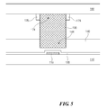
- FIG. 5 is a cross-sectional view of a portion taken along line V-V of FIG. 4 ;
- FIG. 6 is a cross-sectional view of a portion taken along line VI-VI of FIG. 4 ;
- FIG. 7 is a schematic cross-sectional view of a pixel region of the LCD device according to the first embodiment of the present invention.
- FIG. 8 is a schematic plan view of an LCD device according to a second embodiment of the present invention.
- FIG. 9 is a cross-sectional view of a portion taken along line IX-IX of FIG. 8 ;
- FIG. 10 is a cross-sectional view of a portion taken along line X-X of FIG. 8 ;
- FIG. 11 is a schematic cross-sectional view of a pixel region of the LCD device according to the second embodiment of the present invention.
- FIG. 4 is a schematic plan view of a liquid crystal display (LCD) device according to a first embodiment of the present invention
- FIG. 5 is a cross-sectional view of a portion taken along line V-V of FIG. 4
- FIG. 6 is a cross-sectional view of a portion taken along line VI-VI of FIG. 4
- FIG. 7 is a schematic cross-sectional view of a pixel region of the LCD device according to the first embodiment of the present invention.
- the LCD device may include a first substrate 110 , a second substrate 160 , an LC layer 180 , and a seal pattern 190 .
- a thin film transistor (TFT) Tr serving as a switching device and a pixel electrode 150 may be formed on the first substrate 110 .
- the second substrate 160 on which a common electrode 166 may be formed may be disposed opposite the first substrate 110 .
- the LC layer 180 may be interposed between the first and second substrates 110 and 160 .
- the seal pattern 190 may bond the first and second substrates 110 and 160 to each other to prevent leakage of LCs from the LC layer 180 .
- a display region DR and a non-display region NDR may be defined on the first substrate 110 .
- the display region DR may be configured to display images, and the non-display region NDR may be disposed adjacent to the display region DR.
- the seal pattern 190 may be formed in a seal pattern region (not shown) disposed in the non-display region NDR.
- Gate lines 112 and data lines 130 may be formed on the first substrate 110 to enable switching operations of the TFT Tr.
- a driver configured to apply signals to the gate lines 112 and the data lines 130 may be formed on at least one side of the first substrate 110 .
- the second substrate 160 may have a smaller size than the first substrate 110 and expose at least one side of the first substrate 110 .
- the gate lines 112 and the data lines 130 may intersect to define a plurality of pixel regions P on the display region DR.
- the TFT Tr serving as a switching device and the pixel electrode 150 may be formed in each of the pixel regions P.
- the TFT Tr may include a gate electrode 114 connected to the gate line 112 , a gate insulating layer 120 covering the gate electrode 114 , a semiconductor layer 122 including an active layer 122 a disposed on the gate insulating layer 120 and formed of pure a-Si and an ohmic contact layer 122 b formed of doped a-Si, a source electrode 132 disposed on the semiconductor layer 122 and connected to the data line 130 , and a drain electrode 134 disposed on the semiconductor layer 122 and spaced apart from the source electrode 132 .
- a protection layer 140 having a drain contact hole 142 exposing the drain electrode 134 may be formed to cover the TFT Tr.
- the pixel electrode 150 may be formed on the protection layer 140 and connected to the drain electrode 134 through the drain contact hole 142 .
- a gate link line 116 and a gate pad 118 may be formed in the non-display region NDR disposed on one side of the first substrate 110 .
- the gate link line 116 may extend from the gate line 112 , and the gate pad 118 may be connected to an end of the gate link line 116 .
- a gate pad electrode may be formed of the same material in the same layer as the pixel electrode 150 and connected to the gate pad 118 .
- the gate insulating layer 120 and the protection layer 140 may be stacked to cover the gate link line 118 .
- a data link line 136 and a data pad 138 may be formed in the non-display region NDR disposed on the other side of the first substrate 110 .
- the data link line 136 may extend from the data line 130 , and the data pad 138 may be connected to an end of the data link line 136 .
- a data pad electrode may be formed of the same material in the same layer as the pixel electrode 150 and connected to the data pad 138 .
- the gate insulating layer 120 may be disposed under the data link line 136 , and the protection layer 140 may cover the data link line 136 .
- a portion of the protection layer 140 corresponding to the gate link line 116 and the data link line 136 may be etched so that a first seal pattern groove 144 may be formed in the seal pattern region (not shown). That is, when the protection layer 140 has a first thickness, the protection layer 140 may have a second thickness smaller than the first thickness due to the first seal pattern groove 144 . In other words, the protection layer 140 may have a first height from the first substrate 110 in the seal pattern region and have a second height greater than the first height from the first substrate 110 in the remaining region.
- the etching of the protection layer 140 may include a process of completely removing the protection layer 140 to form the drain contact hole 142 and a process of removing only a portion of the protection layer 140 to form the first seal pattern groove 144 .
- the protection layer 140 may be etched using a halftone mask to improve process efficiency. That is, a mask process may be performed using a mask having a transmission unit, a light blocking unit, and a semi-transmission unit so that a portion of the protection layer 140 corresponding to the transmission unit can be completely removed and a portion of the protection layer 140 corresponding to the semi-transmission unit can be partially etched.
- the gate insulating layer 120 and the data link line 136 may be exposed through the first seal pattern groove 144 . However, only a portion of the protection layer 140 may be exposed to prevent the data link line 136 from being exposed and damaged during the etching of the protection layer 140 .
- FIGS. 5 through 7 illustrate the protection layer 140 having a single structure
- the protection layer 140 may have a double structure including upper and lower layers, and only the upper layer of the protection layer 140 may be etched.
- a lower layer formed of an inorganic insulating material such as silicon oxide or silicon nitride
- an upper layer formed of an organic insulating material such as photoacryl or benzocyclobutene (BCB)
- BCB photoacryl or benzocyclobutene
- a black matrix 162 , a color filter layer 164 , and a common electrode 166 may be formed on the second substrate 160 disposed opposite the first substrate 110 .
- the black matrix 162 may be configured to cover the TFT Tr, the gate line 112 , and the data line 130 .
- the color filter layer 164 may correspond to the pixel region P, and the common electrode 16 may be configured to form an electric field along with the pixel electrode 150 .
- the black matrix 162 and the color filter layer 164 may be omitted or formed on the first substrate 110 .
- the common electrode 166 may be formed on the first substrate 110 along with the pixel electrode 150 to form an in-plane switching-mode or fringe-field-switching (FFS)-mode structure.
- FFS fringe-field-switching
- a spacer 172 configured to maintain a cell gap may be formed in the display region DR, and first and second dams 176 and 178 may be formed in the non-display region NDR to correspond to both ends of the first seal pattern groove 144 , thereby forming a second seal pattern groove 174 corresponding to the first seal pattern groove 144 .
- the first and second dams 176 and 178 may be formed of the same material in the same layer as the spacer 172 .
- the formation of the first and second dams 176 and 178 may be performed using a semi-transmission mask process so that the spacer 172 can have a different height from the first and second dams 176 and 178 .
- the first and second dams 176 and 178 may be formed of the same material in the same layer as the color filter layer 164 .
- the first and second dams 176 and 178 may include a single layer formed of any one of materials forming the R, G, and B color filter patterns, or include a double or triple layer formed by stacking at least two of materials forming the R, G, and B color filter patterns.
- first and second dams 176 and 178 may be continuously formed along the seal pattern 190 or a plurality of first and second dams 176 and 178 may be formed apart from one another.
- the LC layer 180 may be interposed between the first and second substrates 110 and 160 , that is, between the pixel electrode 150 and the common electrode 166 , and LC molecules of the LC layer 180 may be driven due to an electric field formed between the pixel electrode 150 and the common electrode 166 .
- the seal pattern 190 may be formed in the non-display region NDR to prevent leakage of LCs from the LC layer 180 and bond the first and second substrates 110 and 160 to each other.
- One end of the seal pattern 190 may be inserted into the first seal pattern groove 144 formed in the protection layer 140 , while the other thereof may be inserted into the second seal pattern groove 174 interposed between the first and second dams 176 and 178 . Due to the above-described construction, even if a sealant is coated with the dispenser located in an undesired second position (refer to PO 2 in FIG. 3B ) or third position (refer to PO 3 in FIG. 3C ), the seal pattern 190 may be formed in a position corresponding to the first and second sealant grooves 144 and 174 during a bonding process.
- the area of the non-display region NDR may be decreased. That is, a narrow-bezel-type LCD device may be provided.
- the width of a seal pattern should be reduced to embody a narrow bezel.
- the width of the seal pattern may be reduced by reducing the amount of the sealant coated using the dispenser, there may be a technical limit to reducing the width of the seal pattern while maintaining a cell gap.
- a second embodiment of the present invention proposes a structure in which the width of a seal pattern is further reduced and the seal pattern has a uniform thickness throughout an LCD device.
- FIG. 8 is a schematic plan view of an LCD device according to a second embodiment of the present invention
- FIG. 9 is a cross-sectional view of a portion taken along line IX-IX of FIG. 8
- FIG. 10 is a cross-sectional view of a portion taken along line X-X of FIG. 8
- FIG. 11 is a schematic cross-sectional view of a pixel region of the LCD device according to the second embodiment of the present invention.
- the LCD device may include a first substrate 210 , a second substrate 260 , an LC layer 280 , and a seal pattern 290 .
- a TFT Tr serving as a switching device and a pixel electrode 250 may be formed on the first substrate 210 .
- the second substrate 260 on which a common electrode 266 is formed may be disposed opposite the first substrate 210 .
- the LC layer 280 may be interposed between the first and second substrates 210 and 260 .
- the seal pattern 290 may bond the first and second substrates 210 and 260 to each other to prevent leakage of LCs from the LC layer 280 .
- a display region DR and a non-display region NDR may be defined on the first substrate 210 .
- the display region DR may be configured to display images, and the non-display region NDR may be disposed adjacent to the display region DR.
- the seal pattern 290 may be formed in a seal pattern region (not shown) disposed in the non-display region NDR.
- Gate lines 212 and data lines 230 may be formed on the first substrate 210 to enable switching operations of the TFT Tr, and a driver configured to apply signals to the gate lines 212 and the data lines 230 may be formed on at least one side of the first substrate 210 .
- the second substrate 260 may have a smaller size than the first substrate 210 and expose at least one side of the first substrate 210 .
- the gate lines 212 and the data lines 230 may intersect on the display region DR to define a plurality of pixel regions P, and the TFT Tr serving as a switching device and a pixel electrode 250 may be formed in each of the pixel regions P.
- the TFT Tr may include a gate electrode 214 connected to the gate line 212 , a gate insulating layer 220 covering the gate electrode 214 , a semiconductor layer 222 including an active layer 222 a disposed on the gate insulating layer 220 and formed of pure a-Si and an ohmic contact layer 222 b formed of doped a-Si, a source electrode 232 disposed on the semiconductor layer 222 and connected to the data line 230 , and a drain electrode 234 disposed on the semiconductor layer 222 and spaced apart from the source electrode 232 .
- a protection layer 240 having a drain contact hole 242 exposing the drain electrode 234 may be formed to cover the TFT Tr, and the pixel electrode 250 may be formed on the protection layer 240 and connected to the drain electrode 234 through the drain contact hole 242 .
- a gate link line 216 and a gate pad 218 may be formed on the non-display region NDR disposed on one side of the first substrate 210 .
- the gate link line 216 may extend from the gate line 212 , and the gate pad 218 may be connected to an end of the gate link line 216 .
- a gate pad electrode may be formed of the same material in the same line as the pixel electrode 250 and connected to the gate pad 218 .
- the gate insulating layer 220 and the protection layer 240 may be stacked to cover the gate link line 218 .
- a data link line 236 and a data pad 238 may be formed on the non-display region NDR disposed on the other side of the first substrate 210 .
- the data link line 236 may be connected to the data line 230
- the data pad 238 may be connected to an end of the data link line 236 .
- the data line 230 may be connected to the data link line 236 through a data line contact hole 224 .
- a data pad electrode may be formed of the same material in the same layer as the pixel electrode 250 and connected to the data pad 238 .
- the gate insulating layer 220 and the protection layer 240 may be stacked to cover the data link line 238 .
- portions of the protection layer 240 and the gate insulating layer 220 corresponding to the gate link line 216 and the data link line 236 may be completely removed to form a first seal pattern groove 244 . That is, the portions of the protection layer 240 and the gate insulating layer 220 corresponding to a region in which the seal pattern 290 will be formed may be completely removed to form the first seal pattern groove 244 .
- the gate link line 216 and the data link line 236 may be exposed through the first seal pattern groove 244 .
- the thickness of the seal pattern 290 may increase. Accordingly, when a predetermined amount of sealant is coated, the width of the seal pattern 290 may be reduced due to the increase in the thickness thereof, so that a narrow bezel can be embodied.
- the data link line 236 may extend from the data line 230 and be disposed in the same layer as the data line 230 so that a portion of the first seal pattern groove 244 corresponding to the gate link line 216 and a portion of the first seal pattern groove 244 corresponding to the data link line 236 can have different depths.
- the gate link line 216 may be stacked on the first substrate 210 in the portion of the first seal pattern groove 244 corresponding to the gate link line 216
- the gate insulating layer 220 and the data link line 236 may be stacked on the first substrate 210 in the portion of the first seal pattern groove 244 corresponding to the data link line 236 .
- the portion of the first seal pattern groove 244 corresponding to the gate link line 216 and the portion of the first seal pattern groove 244 corresponding to the data link line 236 may have different depths.
- a deviation in the thickness of the seal pattern 290 may occur so that portions of the first and second substrates 210 and 260 cannot be completely bonded to each other.
- the data link line 236 may be formed in the same layer as the gate link line 216 so that a difference in the depth of the first seal pattern groove 244 can be prevented from occurring.
- the first seal pattern groove 244 may be formed by completely removing the protection layer 240 and the gate insulating layer 220 so that the width of the seal pattern 290 may be removed to embody a narrow bezel.
- the data link line 236 may be formed in the same layer as the gate link line 216 so that the thickness of the seal pattern 290 can be uniformized.
- a black matrix 262 , a color filter 264 , and a common electrode 266 may be formed on the second substrate 260 disposed opposite the first substrate 210 .
- the black matrix 262 may be configured to cover the TFT Tr, the gate line 212 , and the data line 230 , the color filter layer 264 may correspond to the pixel region P, and the common electrode 266 may be configured to form an electric field along with the pixel electrode 250 .
- the black matrix 262 and the color filter layer 264 may be omitted or formed on the first substrate 210 .
- a spacer 272 configured to maintain a cell gap may be formed on the display region DR, and first and second dams 276 and 278 may be formed in the non-display region NDR to correspond to both ends of the first seal pattern groove 244 , thereby forming a second seal pattern groove 274 corresponding to the first seal pattern groove 244 .
- first and second dams 276 and 278 may be formed of the same material in the same layer as the spacer 272 .
- the formation of the first and second dams 276 and 278 may be performed using a semi-transmission mask process so that the spacer 272 can have a different height from the first and second dams 276 and 278 .
- the first and second dams 276 and 278 may be formed of the same material in the same layer as the color filter layer 264 .
- the first and second dams 276 and 278 may include a single layer formed of any one of materials forming the R, G, and B color filter patterns, or include a double or triple layer formed by stacking at least two of materials forming the R, G, and B color filter patterns.
- first and second dams 276 and 278 may be continuously formed along the seal pattern 290 or a plurality of first and second dams 276 and 278 may be formed apart from one another.
- the LC layer 280 may be interposed between the first and second substrates 210 and 260 , that is, between the pixel electrode 250 and the common electrode 266 , and LC molecules of the LC layer 280 may be driven due to an electric field formed between the pixel electrode 250 and the common electrode 266 .
- the common electrode 266 may be formed on the first substrate 210 along with the pixel electrode 250 to form an in-plane switching-mode or FFS-mode structure.
- the seal pattern 290 may be formed in the non-display region NDR to prevent leakage of LCs from the LC layer 280 and bond the first and second substrates 210 and 260 to each other.
- One end of the seal pattern 290 may be inserted into the first seal pattern groove 244 formed in the protection layer 240 and the gate insulating layer 220 , while the other thereof may be inserted into the second seal pattern groove 274 interposed between the first and second dams 276 and 278 .
- the seal pattern 290 may be formed in a position corresponding to the first and second sealant grooves 244 and 274 during a bonding process.
- the area of the non-display region NDR may be decreased. That is, a narrow-bezel-type LCD device may be provided.
- An LCD device may further include a structure capable of determining a position of the seal pattern and prevent occurrence of errors in the position of the seal pattern, thereby embodying a narrow bezel.
- the width of a bezel may be further reduced by preventing an increase in the thickness of the seal pattern, that is, by reducing the width of the seal pattern, and occurrence of a difference in the thickness of the seal pattern may be prevented. Accordingly, a failure in the bonding of upper and lower substrates caused by the difference in the thickness of the seal pattern may be prevented.
- a groove in which a seal pattern is formed can be formed by etching a protection layer formed on a lower substrate.
- a groove can be formed in a protection layer by etching only a portion of the protection layer, damage to a data link line disposed under the protection layer can be prevented.
- a groove is formed by removing a protection layer and a gate insulating layer disposed under the protection layer, the thickness of a seal pattern can increase, and the width of the seal pattern can be reduced so that the area of a non-display region can be further reduced.
- a data link line can be formed in the same layer as a gate line so that the thickness of the seal pattern can be uniformized.
Landscapes
- Physics & Mathematics (AREA)
- Nonlinear Science (AREA)
- Mathematical Physics (AREA)
- Chemical & Material Sciences (AREA)
- Crystallography & Structural Chemistry (AREA)
- General Physics & Mathematics (AREA)
- Optics & Photonics (AREA)
- Liquid Crystal (AREA)
- Devices For Indicating Variable Information By Combining Individual Elements (AREA)
Applications Claiming Priority (2)
| Application Number | Priority Date | Filing Date | Title |
|---|---|---|---|
| KR10-2012-0077145 | 2012-07-16 | ||
| KR1020120077145A KR102049732B1 (ko) | 2012-07-16 | 2012-07-16 | 액정표시장치 |
Publications (2)
| Publication Number | Publication Date |
|---|---|
| US20140016070A1 US20140016070A1 (en) | 2014-01-16 |
| US9235085B2 true US9235085B2 (en) | 2016-01-12 |
Family
ID=47520727
Family Applications (1)
| Application Number | Title | Priority Date | Filing Date |
|---|---|---|---|
| US13/723,549 Active 2033-06-27 US9235085B2 (en) | 2012-07-16 | 2012-12-21 | Liquid crystal display device |
Country Status (4)
| Country | Link |
|---|---|
| US (1) | US9235085B2 (fr) |
| EP (2) | EP2687901B1 (fr) |
| KR (1) | KR102049732B1 (fr) |
| CN (1) | CN103543561B (fr) |
Families Citing this family (12)
| Publication number | Priority date | Publication date | Assignee | Title |
|---|---|---|---|---|
| KR102054233B1 (ko) | 2012-12-26 | 2019-12-10 | 엘지디스플레이 주식회사 | 액정표시장치 및 그 제조방법 |
| KR20160017273A (ko) * | 2014-08-01 | 2016-02-16 | 삼성디스플레이 주식회사 | 디스플레이 장치와, 이의 제조 방법 |
| CN105045010B (zh) * | 2015-08-26 | 2019-01-22 | 深圳市华星光电技术有限公司 | 一种阵列基板和显示装置 |
| KR102512479B1 (ko) * | 2015-11-27 | 2023-03-21 | 엘지디스플레이 주식회사 | 홀로그램 디스플레이 |
| CN105652528A (zh) * | 2016-01-27 | 2016-06-08 | 京东方科技集团股份有限公司 | 一种显示面板、显示装置及其驱动方法 |
| KR102621568B1 (ko) * | 2016-11-30 | 2024-01-05 | 엘지디스플레이 주식회사 | 협 베젤 표시장치 |
| KR102046297B1 (ko) * | 2017-11-09 | 2019-11-19 | 엘지디스플레이 주식회사 | 표시장치 |
| CN108051957A (zh) * | 2018-01-03 | 2018-05-18 | 京东方科技集团股份有限公司 | 一种基板、显示面板及显示装置 |
| CN109445156A (zh) * | 2018-12-24 | 2019-03-08 | 惠科股份有限公司 | 显示面板、显示装置及显示面板制造方法 |
| KR20210059119A (ko) | 2019-11-14 | 2021-05-25 | 삼성디스플레이 주식회사 | 표시 장치 및 렌티큘러 렌즈 패널의 제조방법 |
| CN111913325B (zh) * | 2020-08-19 | 2022-07-01 | 惠科股份有限公司 | 显示面板与其制造方法、显示装置 |
| CN212808868U (zh) * | 2020-10-16 | 2021-03-26 | 京东方科技集团股份有限公司 | 液晶显示面板和显示装置 |
Citations (8)
| Publication number | Priority date | Publication date | Assignee | Title |
|---|---|---|---|---|
| US20050073638A1 (en) * | 2003-10-06 | 2005-04-07 | Lg.Philips Lcd Co., Ltd. | Liquid crystal display device and method for fabricating the same |
| US20060170854A1 (en) * | 2005-02-01 | 2006-08-03 | Samsung Electronics Co., Ltd. | Liquid crystal display and method of fabricating the same |
| US20080117344A1 (en) * | 2006-11-17 | 2008-05-22 | Samsung Electronics Co., Ltd. | Liquid crystal display panel, method for fabricating the same, and thin film transistor substrate |
| JP2008158169A (ja) | 2006-12-22 | 2008-07-10 | Sharp Corp | 液晶表示パネル及びその製造方法 |
| US7417703B2 (en) * | 2002-12-31 | 2008-08-26 | Lg Display Co., Ltd. | Liquid crystal display device using seal pattern and fabricating method thereof |
| WO2012074010A1 (fr) | 2010-12-03 | 2012-06-07 | シャープ株式会社 | Panneau d'affichage à cristaux liquides et dispositif d'affichage à cristaux liquides |
| US8334963B2 (en) * | 2006-06-07 | 2012-12-18 | Sharp Kabushiki Kaisha | Display comprising a plurality of spacer rows having first and second protruding portions and method of manufacturing the same |
| US8379179B2 (en) * | 2009-12-01 | 2013-02-19 | Samsung Display Co., Ltd. | Flat panel display having particular compensating parts for a thickness difference between sealants |
Family Cites Families (8)
| Publication number | Priority date | Publication date | Assignee | Title |
|---|---|---|---|---|
| JPH11264970A (ja) * | 1998-03-17 | 1999-09-28 | Casio Comput Co Ltd | 液晶表示装置 |
| KR100870660B1 (ko) * | 2001-12-31 | 2008-11-26 | 엘지디스플레이 주식회사 | 패널의 합착력이 향상된 액정표시소자 및 제조방법 |
| KR101116817B1 (ko) * | 2004-06-30 | 2012-02-28 | 엘지디스플레이 주식회사 | 유기 절연막을 포함하는 액정 패널 및 그 제조 방법 |
| KR20060104093A (ko) * | 2005-03-29 | 2006-10-09 | 삼성전자주식회사 | 액정 표시 장치 및 그 제조 방법 |
| JP2007264249A (ja) * | 2006-03-28 | 2007-10-11 | Seiko Epson Corp | 電気光学装置の製造方法、電気光学装置及び電子機器 |
| JP5006637B2 (ja) | 2006-12-22 | 2012-08-22 | キヤノン株式会社 | ズームレンズ及びそれを有する画像投射装置 |
| CN102262319B (zh) * | 2010-05-24 | 2015-02-25 | 北京京东方光电科技有限公司 | 液晶显示基板及其制造方法、液晶面板和液晶显示器 |
| CN202166809U (zh) * | 2011-08-05 | 2012-03-14 | 北京京东方光电科技有限公司 | 一种薄膜晶体管液晶显示屏及显示装置 |
-
2012
- 2012-07-16 KR KR1020120077145A patent/KR102049732B1/ko active IP Right Grant
- 2012-12-14 EP EP12197342.4A patent/EP2687901B1/fr active Active
- 2012-12-14 EP EP14179374.5A patent/EP2813885B1/fr active Active
- 2012-12-21 US US13/723,549 patent/US9235085B2/en active Active
- 2012-12-25 CN CN201210599163.7A patent/CN103543561B/zh active Active
Patent Citations (9)
| Publication number | Priority date | Publication date | Assignee | Title |
|---|---|---|---|---|
| US7417703B2 (en) * | 2002-12-31 | 2008-08-26 | Lg Display Co., Ltd. | Liquid crystal display device using seal pattern and fabricating method thereof |
| US20050073638A1 (en) * | 2003-10-06 | 2005-04-07 | Lg.Philips Lcd Co., Ltd. | Liquid crystal display device and method for fabricating the same |
| US20060170854A1 (en) * | 2005-02-01 | 2006-08-03 | Samsung Electronics Co., Ltd. | Liquid crystal display and method of fabricating the same |
| US8334963B2 (en) * | 2006-06-07 | 2012-12-18 | Sharp Kabushiki Kaisha | Display comprising a plurality of spacer rows having first and second protruding portions and method of manufacturing the same |
| US20080117344A1 (en) * | 2006-11-17 | 2008-05-22 | Samsung Electronics Co., Ltd. | Liquid crystal display panel, method for fabricating the same, and thin film transistor substrate |
| JP2008158169A (ja) | 2006-12-22 | 2008-07-10 | Sharp Corp | 液晶表示パネル及びその製造方法 |
| US8379179B2 (en) * | 2009-12-01 | 2013-02-19 | Samsung Display Co., Ltd. | Flat panel display having particular compensating parts for a thickness difference between sealants |
| WO2012074010A1 (fr) | 2010-12-03 | 2012-06-07 | シャープ株式会社 | Panneau d'affichage à cristaux liquides et dispositif d'affichage à cristaux liquides |
| US20130250227A1 (en) | 2010-12-03 | 2013-09-26 | Sharp Kabushiki Kaisha | Liquid crystal display panel and liquid crystal display device |
Non-Patent Citations (1)
| Title |
|---|
| Extended European Search Report dated Oct. 11, 2013 for Application No. 12197342.4. |
Also Published As
| Publication number | Publication date |
|---|---|
| EP2813885A3 (fr) | 2015-01-14 |
| EP2813885B1 (fr) | 2017-02-15 |
| EP2687901A1 (fr) | 2014-01-22 |
| CN103543561A (zh) | 2014-01-29 |
| KR102049732B1 (ko) | 2019-11-29 |
| US20140016070A1 (en) | 2014-01-16 |
| KR20140010634A (ko) | 2014-01-27 |
| CN103543561B (zh) | 2017-11-17 |
| EP2813885A2 (fr) | 2014-12-17 |
| EP2687901B1 (fr) | 2018-10-10 |
Similar Documents
| Publication | Publication Date | Title |
|---|---|---|
| US9235085B2 (en) | Liquid crystal display device | |
| US10983400B2 (en) | Liquid crystal display device | |
| US8102489B2 (en) | Liquid crystal display device having black matrix in region outside of pixel region and method for fabricating the same | |
| US7528917B2 (en) | Liquid crystal display device having structure of color filter on TFT and using in plane switching mode | |
| US8253891B2 (en) | Thin film transistor substrate and liquid crystal display including the same | |
| KR20140083650A (ko) | 액정표시장치 및 그 제조방법 | |
| KR20080081426A (ko) | 표시 장치 및 그의 제조 방법 | |
| US20090237581A1 (en) | Liquid crystal display and method for manufacturing the same | |
| JP2000243963A (ja) | 薄膜トランジスタ及び表示装置 | |
| JP2004272012A (ja) | 表示装置 | |
| US7098986B2 (en) | Data pad region of liquid crystal display panel and fabricating method thereof | |
| US6967703B2 (en) | Liquid crystal display device and method thereof | |
| US20130342780A1 (en) | Display substrate, a method of manufacturing the same and a display apparatus having the same | |
| KR100874646B1 (ko) | 액정표시장치 및 그 제조방법 | |
| US8330929B2 (en) | Display panel | |
| KR101232166B1 (ko) | 액정표시장치 및 그의 제조방법 | |
| KR100983579B1 (ko) | 액정표시장치 및 그의 제조방법 | |
| KR101001453B1 (ko) | 박막트랜지스터 어레이 기판 및 그 제조 방법 | |
| KR20070082325A (ko) | 박막 트랜지스터 기판 및 이의 제조 방법 및 액정 표시장치 | |
| KR20050004547A (ko) | 액정표시패널 | |
| KR101258084B1 (ko) | 액정표시소자 및 그 제조방법 | |
| KR20050066347A (ko) | 액정 표시 장치 및 제조 방법 | |
| KR20060131318A (ko) | 액정표시패널 및 그 제조방법 | |
| JP2001027766A (ja) | 反射型液晶表示装置 |
Legal Events
| Date | Code | Title | Description |
|---|---|---|---|
| AS | Assignment |
Owner name: LG DISPLAY CO., LTD., KOREA, REPUBLIC OF Free format text: ASSIGNMENT OF ASSIGNORS INTEREST;ASSIGNORS:CHOI, WON-JUN;BAEK, SE-JOON;NAM, SUNG-LIM;AND OTHERS;SIGNING DATES FROM 20121213 TO 20121217;REEL/FRAME:029519/0722 |
|
| FEPP | Fee payment procedure |
Free format text: PAYOR NUMBER ASSIGNED (ORIGINAL EVENT CODE: ASPN); ENTITY STATUS OF PATENT OWNER: LARGE ENTITY |
|
| STCF | Information on status: patent grant |
Free format text: PATENTED CASE |
|
| MAFP | Maintenance fee payment |
Free format text: PAYMENT OF MAINTENANCE FEE, 4TH YEAR, LARGE ENTITY (ORIGINAL EVENT CODE: M1551); ENTITY STATUS OF PATENT OWNER: LARGE ENTITY Year of fee payment: 4 |
|
| MAFP | Maintenance fee payment |
Free format text: PAYMENT OF MAINTENANCE FEE, 8TH YEAR, LARGE ENTITY (ORIGINAL EVENT CODE: M1552); ENTITY STATUS OF PATENT OWNER: LARGE ENTITY Year of fee payment: 8 |