US9064458B2 - Organic light emitting display and driving method thereof - Google Patents
Organic light emitting display and driving method thereof Download PDFInfo
- Publication number
- US9064458B2 US9064458B2 US12/786,254 US78625410A US9064458B2 US 9064458 B2 US9064458 B2 US 9064458B2 US 78625410 A US78625410 A US 78625410A US 9064458 B2 US9064458 B2 US 9064458B2
- Authority
- US
- United States
- Prior art keywords
- power
- pixels
- signals
- scan
- electrode
- Prior art date
- Legal status (The legal status is an assumption and is not a legal conclusion. Google has not performed a legal analysis and makes no representation as to the accuracy of the status listed.)
- Active, expires
Links
Images


Classifications
-
- G—PHYSICS
- G09—EDUCATION; CRYPTOGRAPHY; DISPLAY; ADVERTISING; SEALS
- G09G—ARRANGEMENTS OR CIRCUITS FOR CONTROL OF INDICATING DEVICES USING STATIC MEANS TO PRESENT VARIABLE INFORMATION
- G09G3/00—Control arrangements or circuits, of interest only in connection with visual indicators other than cathode-ray tubes
- G09G3/20—Control arrangements or circuits, of interest only in connection with visual indicators other than cathode-ray tubes for presentation of an assembly of a number of characters, e.g. a page, by composing the assembly by combination of individual elements arranged in a matrix no fixed position being assigned to or needed to be assigned to the individual characters or partial characters
- G09G3/22—Control arrangements or circuits, of interest only in connection with visual indicators other than cathode-ray tubes for presentation of an assembly of a number of characters, e.g. a page, by composing the assembly by combination of individual elements arranged in a matrix no fixed position being assigned to or needed to be assigned to the individual characters or partial characters using controlled light sources
- G09G3/30—Control arrangements or circuits, of interest only in connection with visual indicators other than cathode-ray tubes for presentation of an assembly of a number of characters, e.g. a page, by composing the assembly by combination of individual elements arranged in a matrix no fixed position being assigned to or needed to be assigned to the individual characters or partial characters using controlled light sources using electroluminescent panels
- G09G3/32—Control arrangements or circuits, of interest only in connection with visual indicators other than cathode-ray tubes for presentation of an assembly of a number of characters, e.g. a page, by composing the assembly by combination of individual elements arranged in a matrix no fixed position being assigned to or needed to be assigned to the individual characters or partial characters using controlled light sources using electroluminescent panels semiconductive, e.g. using light-emitting diodes [LED]
- G09G3/3208—Control arrangements or circuits, of interest only in connection with visual indicators other than cathode-ray tubes for presentation of an assembly of a number of characters, e.g. a page, by composing the assembly by combination of individual elements arranged in a matrix no fixed position being assigned to or needed to be assigned to the individual characters or partial characters using controlled light sources using electroluminescent panels semiconductive, e.g. using light-emitting diodes [LED] organic, e.g. using organic light-emitting diodes [OLED]
- G09G3/3225—Control arrangements or circuits, of interest only in connection with visual indicators other than cathode-ray tubes for presentation of an assembly of a number of characters, e.g. a page, by composing the assembly by combination of individual elements arranged in a matrix no fixed position being assigned to or needed to be assigned to the individual characters or partial characters using controlled light sources using electroluminescent panels semiconductive, e.g. using light-emitting diodes [LED] organic, e.g. using organic light-emitting diodes [OLED] using an active matrix
- G09G3/3258—Control arrangements or circuits, of interest only in connection with visual indicators other than cathode-ray tubes for presentation of an assembly of a number of characters, e.g. a page, by composing the assembly by combination of individual elements arranged in a matrix no fixed position being assigned to or needed to be assigned to the individual characters or partial characters using controlled light sources using electroluminescent panels semiconductive, e.g. using light-emitting diodes [LED] organic, e.g. using organic light-emitting diodes [OLED] using an active matrix with pixel circuitry controlling the voltage across the light-emitting element
-
- G—PHYSICS
- G09—EDUCATION; CRYPTOGRAPHY; DISPLAY; ADVERTISING; SEALS
- G09G—ARRANGEMENTS OR CIRCUITS FOR CONTROL OF INDICATING DEVICES USING STATIC MEANS TO PRESENT VARIABLE INFORMATION
- G09G3/00—Control arrangements or circuits, of interest only in connection with visual indicators other than cathode-ray tubes
- G09G3/001—Control arrangements or circuits, of interest only in connection with visual indicators other than cathode-ray tubes using specific devices not provided for in groups G09G3/02 - G09G3/36, e.g. using an intermediate record carrier such as a film slide; Projection systems; Display of non-alphanumerical information, solely or in combination with alphanumerical information, e.g. digital display on projected diapositive as background
- G09G3/003—Control arrangements or circuits, of interest only in connection with visual indicators other than cathode-ray tubes using specific devices not provided for in groups G09G3/02 - G09G3/36, e.g. using an intermediate record carrier such as a film slide; Projection systems; Display of non-alphanumerical information, solely or in combination with alphanumerical information, e.g. digital display on projected diapositive as background to produce spatial visual effects
-
- G—PHYSICS
- G09—EDUCATION; CRYPTOGRAPHY; DISPLAY; ADVERTISING; SEALS
- G09G—ARRANGEMENTS OR CIRCUITS FOR CONTROL OF INDICATING DEVICES USING STATIC MEANS TO PRESENT VARIABLE INFORMATION
- G09G3/00—Control arrangements or circuits, of interest only in connection with visual indicators other than cathode-ray tubes
- G09G3/20—Control arrangements or circuits, of interest only in connection with visual indicators other than cathode-ray tubes for presentation of an assembly of a number of characters, e.g. a page, by composing the assembly by combination of individual elements arranged in a matrix no fixed position being assigned to or needed to be assigned to the individual characters or partial characters
- G09G3/22—Control arrangements or circuits, of interest only in connection with visual indicators other than cathode-ray tubes for presentation of an assembly of a number of characters, e.g. a page, by composing the assembly by combination of individual elements arranged in a matrix no fixed position being assigned to or needed to be assigned to the individual characters or partial characters using controlled light sources
- G09G3/30—Control arrangements or circuits, of interest only in connection with visual indicators other than cathode-ray tubes for presentation of an assembly of a number of characters, e.g. a page, by composing the assembly by combination of individual elements arranged in a matrix no fixed position being assigned to or needed to be assigned to the individual characters or partial characters using controlled light sources using electroluminescent panels
- G09G3/32—Control arrangements or circuits, of interest only in connection with visual indicators other than cathode-ray tubes for presentation of an assembly of a number of characters, e.g. a page, by composing the assembly by combination of individual elements arranged in a matrix no fixed position being assigned to or needed to be assigned to the individual characters or partial characters using controlled light sources using electroluminescent panels semiconductive, e.g. using light-emitting diodes [LED]
- G09G3/3208—Control arrangements or circuits, of interest only in connection with visual indicators other than cathode-ray tubes for presentation of an assembly of a number of characters, e.g. a page, by composing the assembly by combination of individual elements arranged in a matrix no fixed position being assigned to or needed to be assigned to the individual characters or partial characters using controlled light sources using electroluminescent panels semiconductive, e.g. using light-emitting diodes [LED] organic, e.g. using organic light-emitting diodes [OLED]
- G09G3/3275—Details of drivers for data electrodes
- G09G3/3291—Details of drivers for data electrodes in which the data driver supplies a variable data voltage for setting the current through, or the voltage across, the light-emitting elements
-
- G—PHYSICS
- G09—EDUCATION; CRYPTOGRAPHY; DISPLAY; ADVERTISING; SEALS
- G09G—ARRANGEMENTS OR CIRCUITS FOR CONTROL OF INDICATING DEVICES USING STATIC MEANS TO PRESENT VARIABLE INFORMATION
- G09G2300/00—Aspects of the constitution of display devices
- G09G2300/04—Structural and physical details of display devices
- G09G2300/0421—Structural details of the set of electrodes
- G09G2300/043—Compensation electrodes or other additional electrodes in matrix displays related to distortions or compensation signals, e.g. for modifying TFT threshold voltage in column driver
-
- G—PHYSICS
- G09—EDUCATION; CRYPTOGRAPHY; DISPLAY; ADVERTISING; SEALS
- G09G—ARRANGEMENTS OR CIRCUITS FOR CONTROL OF INDICATING DEVICES USING STATIC MEANS TO PRESENT VARIABLE INFORMATION
- G09G2300/00—Aspects of the constitution of display devices
- G09G2300/08—Active matrix structure, i.e. with use of active elements, inclusive of non-linear two terminal elements, in the pixels together with light emitting or modulating elements
- G09G2300/0809—Several active elements per pixel in active matrix panels
- G09G2300/0842—Several active elements per pixel in active matrix panels forming a memory circuit, e.g. a dynamic memory with one capacitor
- G09G2300/0861—Several active elements per pixel in active matrix panels forming a memory circuit, e.g. a dynamic memory with one capacitor with additional control of the display period without amending the charge stored in a pixel memory, e.g. by means of additional select electrodes
- G09G2300/0866—Several active elements per pixel in active matrix panels forming a memory circuit, e.g. a dynamic memory with one capacitor with additional control of the display period without amending the charge stored in a pixel memory, e.g. by means of additional select electrodes by means of changes in the pixel supply voltage
-
- G—PHYSICS
- G09—EDUCATION; CRYPTOGRAPHY; DISPLAY; ADVERTISING; SEALS
- G09G—ARRANGEMENTS OR CIRCUITS FOR CONTROL OF INDICATING DEVICES USING STATIC MEANS TO PRESENT VARIABLE INFORMATION
- G09G2310/00—Command of the display device
- G09G2310/06—Details of flat display driving waveforms
- G09G2310/061—Details of flat display driving waveforms for resetting or blanking
- G09G2310/063—Waveforms for resetting the whole screen at once
-
- G—PHYSICS
- G09—EDUCATION; CRYPTOGRAPHY; DISPLAY; ADVERTISING; SEALS
- G09G—ARRANGEMENTS OR CIRCUITS FOR CONTROL OF INDICATING DEVICES USING STATIC MEANS TO PRESENT VARIABLE INFORMATION
- G09G2320/00—Control of display operating conditions
- G09G2320/04—Maintaining the quality of display appearance
- G09G2320/043—Preventing or counteracting the effects of ageing
-
- G—PHYSICS
- G09—EDUCATION; CRYPTOGRAPHY; DISPLAY; ADVERTISING; SEALS
- G09G—ARRANGEMENTS OR CIRCUITS FOR CONTROL OF INDICATING DEVICES USING STATIC MEANS TO PRESENT VARIABLE INFORMATION
- G09G3/00—Control arrangements or circuits, of interest only in connection with visual indicators other than cathode-ray tubes
- G09G3/20—Control arrangements or circuits, of interest only in connection with visual indicators other than cathode-ray tubes for presentation of an assembly of a number of characters, e.g. a page, by composing the assembly by combination of individual elements arranged in a matrix no fixed position being assigned to or needed to be assigned to the individual characters or partial characters
- G09G3/22—Control arrangements or circuits, of interest only in connection with visual indicators other than cathode-ray tubes for presentation of an assembly of a number of characters, e.g. a page, by composing the assembly by combination of individual elements arranged in a matrix no fixed position being assigned to or needed to be assigned to the individual characters or partial characters using controlled light sources
- G09G3/30—Control arrangements or circuits, of interest only in connection with visual indicators other than cathode-ray tubes for presentation of an assembly of a number of characters, e.g. a page, by composing the assembly by combination of individual elements arranged in a matrix no fixed position being assigned to or needed to be assigned to the individual characters or partial characters using controlled light sources using electroluminescent panels
- G09G3/32—Control arrangements or circuits, of interest only in connection with visual indicators other than cathode-ray tubes for presentation of an assembly of a number of characters, e.g. a page, by composing the assembly by combination of individual elements arranged in a matrix no fixed position being assigned to or needed to be assigned to the individual characters or partial characters using controlled light sources using electroluminescent panels semiconductive, e.g. using light-emitting diodes [LED]
- G09G3/3208—Control arrangements or circuits, of interest only in connection with visual indicators other than cathode-ray tubes for presentation of an assembly of a number of characters, e.g. a page, by composing the assembly by combination of individual elements arranged in a matrix no fixed position being assigned to or needed to be assigned to the individual characters or partial characters using controlled light sources using electroluminescent panels semiconductive, e.g. using light-emitting diodes [LED] organic, e.g. using organic light-emitting diodes [OLED]
- G09G3/3225—Control arrangements or circuits, of interest only in connection with visual indicators other than cathode-ray tubes for presentation of an assembly of a number of characters, e.g. a page, by composing the assembly by combination of individual elements arranged in a matrix no fixed position being assigned to or needed to be assigned to the individual characters or partial characters using controlled light sources using electroluminescent panels semiconductive, e.g. using light-emitting diodes [LED] organic, e.g. using organic light-emitting diodes [OLED] using an active matrix
- G09G3/3233—Control arrangements or circuits, of interest only in connection with visual indicators other than cathode-ray tubes for presentation of an assembly of a number of characters, e.g. a page, by composing the assembly by combination of individual elements arranged in a matrix no fixed position being assigned to or needed to be assigned to the individual characters or partial characters using controlled light sources using electroluminescent panels semiconductive, e.g. using light-emitting diodes [LED] organic, e.g. using organic light-emitting diodes [OLED] using an active matrix with pixel circuitry controlling the current through the light-emitting element
Definitions
- An aspect of one embodiment of the present invention is directed to an organic light emitting display, and a driving method thereof.
- the various flat panel displays include a liquid crystal display (LCD), a field emission display (FED), a plasma display panel (PDP), an organic light emitting display, etc.
- LCD liquid crystal display
- FED field emission display
- PDP plasma display panel
- organic light emitting display etc.
- the organic light emitting display which displays an image using organic light emitting diodes (OLEDs) that light-emit light by a re-combination of electrons and holes, has a rapid response speed and low power consumption.
- OLEDs organic light emitting diodes
- organic light emitting displays can be classified as a passive matrix type OLED (PMOLED) display and an active matrix type OLED (AMOLED) display according to a method of driving the OLEDs.
- PMOLED passive matrix type OLED
- AMOLED active matrix type OLED
- the AMOLED display includes a plurality of gate lines, a plurality of data lines, a plurality of power lines, and a plurality of pixels that are coupled to the lines and arranged in a matrix form.
- each of the pixels generally includes an OLED, two transistors, e.g., a switching transistor that transfers a data signal and a driving transistor that drives the OLED according to the data signal, and a capacitor that maintains the data voltage.
- the AMOLED display has low power consumption, but the amount of currents flowing through its OLEDs vary according to deviations in threshold voltage of its transistors to cause display non-uniformity.
- a compensation circuit that includes a plurality of transistors and capacitors can be additionally included in the respective pixels. However, the additional compensation circuit causes additional transistors and capacitors to be added in each pixel.
- the compensation circuit is added in the respective pixels as described above, the transistors and capacitors that constitute each pixel and the signal lines that control the transistors are added so that in a bottom emission type AMOLED display, an aperture ratio is reduced, and the probability that defects are generated is increased due to the increased complexity of the circuit.
- OLED organic light emitting diode
- each pixel includes an OLED and a pixel circuit coupled thereto.
- the pixel circuit includes three transistors and two capacitors, the pixel being driven in a simultaneous (or concurrent) emission scheme, and is able to perform the threshold voltage compensation of the driving transistors provided in the pixels and the high-speed driving thereof, and a driving method thereof.
- an organic light emitting display includes: a display unit including a plurality of pixels coupled to scan lines, control lines, and data lines; a control line driver for providing control signals to the pixels through the control lines; a first power driver for applying a first power to the pixels of the display unit; and a second power driver for applying a second power to the pixels of the display unit.
- the first power and/or the second power is applied to the pixels of the display unit, having voltage values at different levels, during periods of one frame, and the control signals and the first and second powers are concurrently provided to all of the pixels included in the display unit.
- the organic light emitting display may further include: a scan driver for supplying scan signals to the pixels through the scan lines; a data driver for supplying data signals to the pixels through the data lines; and a timing controller for controlling the control line driver, the first power driver, the second power driver, the scan driver, and the data driver.
- the first power driver may be adapted to apply the first power having voltage values at three different levels for each period during the periods of one frame
- the second power driver may be adapted to apply the second power having a voltage value at a fixed level during the all of the periods of one frame.
- the first power driver and the second power driver may be adapted to respectively apply the first and second powers each having voltage values at two different levels for each period during the periods of one frame.
- the first power driver may be adapted to apply the first power having a voltage value at a fixed level for all of the periods of one frame
- the second power driver may be adapted to apply the second power having voltage values at three different levels for each period during the periods of one frame.
- the scan signals may be applied sequentially by each of the scan lines for a partial period of the periods of one frame and may be applied concurrently to the scan lines during the periods other than the partial period.
- Widths of the sequentially applied scan signals may be applied at two horizontal time, and adjacently applied ones of the scan signals may be applied to be overlapped with each other by one horizontal time.
- the data signals may be applied sequentially to the pixels by each of the scan lines corresponding to the sequentially applied scan signals, and the data signals may be concurrently applied to all of the pixels through the data lines during the periods other than the partial period.
- Each of the pixels may include: a first transistor having a gate electrode coupled to a scan line of the scan lines, a first electrode coupled to a data line of the data lines, and a second electrode coupled to a first node; a second transistor having a gate electrode coupled to a second node, a first electrode coupled to the first power, and a second electrode; a first capacitor coupled between the first node and the first electrode of the second transistor; a second capacitor coupled between the first node and the second node; a third transistor having a gate electrode coupled to a control line of the control lines, a first electrode coupled to the gate electrode of the second transistor, and a second electrode coupled to the second electrode of the second transistor; and an organic light emitting diode having an anode electrode coupled to the second electrode of the second transistor and a cathode electrode coupled to the second power.
- the first to third transistors may be PMOS transistors.
- the pixels When the first power and the control signals may be applied at a high level to the pixels included in the display unit, the pixels may be concurrently light-emitted at brightness corresponding to the data signals pre-stored for each of the pixels.
- Each of the pixels may includes a first transistor having a gate electrode coupled to a scan line of the scan lines, a first electrode coupled to a data line of the data lines, and a second electrode coupled to a first node; a second transistor have a gate electrode coupled to a second node, a first electrode coupled to a second power, and a second electrode; a first capacitor coupled between the first node and the first electrode of the second transistor; a second capacitor coupled between the first node and the second node; a third transistor having a gate electrode coupled to a control line of the control lines, a first electrode coupled to the gate electrode of the second transistor, and a second electrode coupled to the second electrode of the second transistor; and an OLED having a cathode electrode coupled to the second electrode of the second transistor and an anode electrode coupled to the first power.
- the first to third transistors may be NMOS transistors.
- Another embodiment of the present invention is directed to a driving method of an organic light emitting display.
- the method includes: (a) initializing voltages of respective nodes of a plurality of pixel circuits included in respective pixels by concurrently applying a first power, a second power, scan signals, control signals, and data signals, having voltage values at respective levels, to all of the pixels that constitute a display unit; (b) dropping a voltage of an anode electrode of an OLED included in the respective pixels below a voltage of a cathode electrode of the OLED by concurrently applying the first power, the second power, the scan signals, the control signals, and the data signals, having the voltage values at respective levels, to all of the pixels; (c) storing a threshold voltage of a driving transistor included in the respective pixels by concurrently applying the first power, the second power, the scan signals, the control signals, and the data signals, having the voltage values at respective levels, to all of the pixels; (d) applying the scan signals sequentially to the pixels coupled to scan lines of the display unit and applying the data
- One frame may be implemented through (a) to (f).
- an nth frame may display a left-eye image and an (n+1) th frame may display a right-eye image.
- An entire time between an emission period of the nth frame and an emission frame of the (n+1) th frame may be synchronized with a response time of a shutter glasses.
- Each of the pixels may includes a first PMOS transistor having a gate electrode coupled to a scan line of the scan lines, a first electrode coupled to a data line, and a second electrode coupled to a first node; a second PMOS transistor having a gate electrode coupled to a second node, a first electrode coupled to the first power, and a second electrode; a first capacitor coupled between the first node and the first electrode of the second transistor; a second capacitor coupled between the first node and the second node; a third PMOS transistor having a gate electrode coupled to a control line, a first electrode coupled to the gate electrode of the second transistor, and a second electrode coupled to the second electrode of the second transistor; and an organic light emitting diode (OLED) having an anode electrode coupled to the second electrode of the second transistor and a cathode electrode coupled to the second power.
- OLED organic light emitting diode
- the first power may be applied at a middle level
- the scan signals may be applied at a low level
- the control signals may be applied at a high level
- (b) may includes: (b1) wherein the first power is applied at a low level, the scan signal may be applied at a high level or a low level, and the control signals may be applied at a high level; (b2) wherein the first power may be applied at a low level, the scan signals may be applied at a high level or a low level, and the control signals may be applied at a high level; (b3) wherein the first power may be applied at a middle level, the scan signals may be applied at a high level or a low level, and the control signals may be applied at a high level.
- the data signals corresponding thereto may be applied at a low level.
- (c) may include: (c1) wherein the first power may be applied at a middle level, the scan signals may be applied at a high level or a low level, and the control signals may be applied at a high level; and (c2) and (c3), wherein the first power may be applied at a middle level, the scan signals may be applied at a low level, and the control signals may be applied at a low level.
- control signals may be applied at a low level.
- widths of the sequentially applied scan signals may be applied at two horizontal time, adjacently applied ones of the scan signals being applied to be overlapped with each other by one horizontal time.
- the first power may be applied at a high level
- the scan signals and the control signals may be applied at a high level
- the first power may be applied at a middle level, and the scan signal and the control signal may be applied at a high level.
- FIG. 1 is a block diagram of an organic light emitting display according to an embodiment of the present invention.
- FIG. 2 is a diagram showing a driving operation in a simultaneous emission scheme according to an embodiment of the present invention
- FIG. 3 is a diagram showing an example where a pair of shutter glasses for 3D display is implemented in a progressive emission scheme according to a related art
- FIG. 4 is a diagram showing an example where a pair of shutter glasses for 3D display is implemented in a simultaneous emission scheme according to an embodiment of the present invention
- FIG. 5 is a graph comparing the duty ratios obtained in the simultaneous emission scheme and the progressive emission scheme
- FIG. 6 is a circuit diagram of a pixel in FIG. 1 according to one embodiment of the present invention.
- FIGS. 7A , 7 B, and 7 C are driving timing diagrams of the pixel in FIG. 6 ;
- FIGS. 8A , 8 B, 8 C, 8 D, 8 E, 8 F, 8 G, 8 H, 8 I, and 8 J are diagrams for explaining the driving of an organic light emitting display according to an embodiment of the present invention.
- FIG. 9 is a circuit diagram of the pixel in FIG. 1 according to another embodiment of the present invention.
- first element when a first element is described as being coupled to a second element, the first element may be directly coupled to the second element or indirectly coupled to the second element via a third element. Further, some of the elements that are not essential to a complete understanding of the invention are omitted for clarity. Also, like reference numerals refer to like elements throughout.
- FIG. 1 is a block diagram of an organic light emitting display according to an embodiment of the present invention
- FIG. 2 is a diagram showing a driving operation in a simultaneous emission scheme according to an embodiment of the present invention.
- the organic light emitting display includes a display unit 130 that includes pixels 140 that are coupled to scan lines S 1 to Sn, control lines GC 1 to GCn and data lines D 1 to Dm, a scan driver 110 that provides scan signals to the respective pixels through the scan lines S 1 to Sn, a control line driver 160 that provides control signals to the respective pixels through the control lines GC 1 to GCn, a data driver 120 that provides data signals to the respective pixels through the data lines D 1 to Dm, and a timing controller 150 that controls the scan driver 110 , the data driver 120 , and the control line driver 160 .
- the pixels 140 are positioned in regions defined by the crossings of the scan lines S 1 to Sn and the data lines D 1 to Dm.
- the pixels 140 receive first power ELVDD and second power ELVSS from the outside.
- Each of the pixels 140 controls the amount of current supplied to the second power ELVSS from the first power ELVDD through an organic light emitting diode (OLED) corresponding to the data signal. Then, light having a brightness (e.g., a predetermined brightness) is generated from the OLED.
- OLED organic light emitting diode
- the first power ELVDD and/or the second power ELVSS is applied to the respective pixels 140 of the display unit at voltage values at different levels during one frame.
- a first power ELVDD driver 170 that controls the supply of the first power ELVDD and/or a second power ELVSS driver 180 that controls the supply of the second power ELVDD are further provided, and the first power ELVDD driver 170 and the second power ELVSS driver 180 are controlled by the timing controller 150 .
- the first power ELVDD is supplied having a voltage at a fixed high level
- the second power ELVSS is supplied having a voltage at a fixed low level to pixels of a display unit.
- the first power ELVDD and the second power ELVSS are applied in accordance with the following three schemes.
- the first power ELVDD is applied having voltage values at three different levels
- the second power ELVSS is applied having a voltage at a fixed low level (for example, ground).
- the second power ELVSS driver 180 outputs the second power ELVSS with a voltage value at an always constant level (e.g., GND) so that there is no need to implement the second power ELVSS driver 180 as a separate driving circuit, thereby making it possible to reduce circuit costs.
- the first power ELVDD has a negative voltage value (for example, ⁇ 3V) as one of the three levels so that the circuit constitution of the first power ELVDD driver 170 may be complicated in the first scheme, however.
- the first power ELVDD and the second power ELVSS are applied each having voltage values at two levels.
- both the first power driver 170 and the second power driver 180 are provided.
- the first power ELVDD is applied having a voltage value at a fixed high level
- the second power ELVSS is applied having voltage values at three different levels, being opposite to the first scheme.
- the first power driver 170 outputs the voltage value at an always constant level so that there is no need to implement the first power driver 170 as a separate driving circuit, thereby making it possible to reduce circuit costs.
- the second power ELVSS has a positive voltage value as one of its three levels so that the circuit constitution of the second power ELVSS driver 180 may be complicated, in the third scheme, however.
- the organic light emitting display is driven in a simultaneous emission scheme rather than in a progressive emission scheme.
- the emission is performed in sequence right after data is input in sequence per scan line.
- the input of the data is performed in sequence, but the emission is concurrently performed with all of the pixels 140 after the input of the data is completed.
- the driving step is divided into (a) an initialization step, (b) a reset step, (c) a threshold voltage compensation step, (d) a scanning step (a data input step), (e) an emission step, and (f) an emission turn-off step.
- the scanning step (the data input step) is performed in sequence per the respective scan lines, but (a) the initialization step, (b) the reset step, (c) the threshold voltage compensation step, (e) the emission step, and (f) the emission turn-off step are performed simultaneously (or concurrently) on the entire display unit 130 .
- the initialization step is a period where voltages at nodes of the pixel circuits respectively provided in the pixels are initialized to be identical with that in inputting the threshold voltage of the driving transistor
- the reset step which is a step where the data voltage applied to each pixel 140 of the display unit 130 is reset, is a period where the voltage of the anode electrode of the OLED of each pixel 140 is dropped below the voltage of the cathode electrode so that the organic light emitting diode is not light-emitted.
- the threshold voltage compensation step is a period where the threshold voltage of the driving transistor provided in each pixel 140 is compensated for
- the emission turn-off step is a period where the emission of each pixel 140 is turned off for a black insertion or a dimming after the emission is performed in each pixel.
- the signals applied during (a) the initialization step, (b) the reset step, (c) the threshold voltage compensation step, (e) the emission step, and (f) the emission turn-off step that is, the scan signals applied to the respective scan lines S 1 to Sn, the first power ELVDD and/or the second power ELVSS applied to the respective pixels 140 , and the control signals applied to the respective control lines GC 1 to GCn are simultaneously (or concurrently) applied to the pixels 140 provided in the display unit 130 at respective voltage levels (e.g., predetermined voltage levels).
- the respective operation periods ((a) to (f) steps) are clearly divided in time. Therefore, the number of the transistors of the compensation circuit provided in the respective pixels 140 and the number of the signal lines that control thereof can be reduced such that the pair of shutter glasses for 3D display can be easily implemented.
- the screen When a user wears the pair of shutter glasses for 3D display that switches transmittance of left eye and right eye between 0% and 100% to see a screen, which is displayed on the display unit of the organic light emitting display, the screen is output as a left-eye image and a right-eye image for each frame so that the user sees the left-eye image with only his or her left-eye and the right-eye image with only his or her right-eye, thereby implementing three-dimensional effects.
- FIG. 3 is a diagram showing an example where a pair of shutter glasses for 3D display is implemented in a progressive emission scheme according to a related art
- FIG. 4 is a diagram showing an example where a pair of shutter glasses for 3D display is implemented in a simultaneous emission scheme according to an embodiment of the present invention.
- FIG. 5 is a graph comparing the duty ratio that can be obtained in the cases of the simultaneous emission scheme and the progressive emission scheme.
- the response time (for example, 2.5 ms) of the pair of shutter glasses is finite (e.g., non-zero) so that the emission of pixels should be turned off during the response time in order to prevent a cross talk phenomenon between the left eye/right eye images.
- a non-light emitting period should be additionally generated between a frame (n th frame) where the left-eye image is output and a frame ((n+1) th frame) where the right-eye image is output during the response time.
- the duty ratio of the emission time becomes lower.
- the light-emitting step is simultaneously (or concurrently) performed on all the pixels as aforementioned, and the non-emission period is performed during the periods other than the light-emitting step so that the non-emission period between the period where the left-eye image is output and the period where the right-eye image is output is naturally provided.
- the emission turn-off period, the reset period, and the threshold voltage compensation period which are the periods between the emission period of the n th frame and the emission period of the (n+1) th frame, are non-light emitted so that if the entire time of these periods are synchronized with the response time (for example, 2.5 ms) of the pair of shutter glasses, there is no need to separately reduce the duty ratio, which is different from the progressive emission scheme according to the related art.
- the “simultaneous emission scheme” can secure the duty ratio by the response time of the pair of shutter glasses as compared to the “progressive emission scheme” according to the related art, making it possible to improve performance as shown in the graph of FIG. 5 .
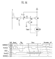
- FIG. 6 is a circuit diagram of the pixel 140 of FIG. 1 according to one embodiment of the present invention
- FIGS. 7A to 7C are driving timing diagrams of the pixel in FIG. 6 .
- the pixel 140 includes an OLED and a pixel circuit 142 that supplies current to the OLED.
- the anode electrode of the OLED is coupled to the pixel circuit 142
- the cathode electrode of the OLED is coupled to a second power ELVSS.
- the OLED generates light having a brightness (e.g., a predetermined brightness) corresponding to the current supplied from the pixel circuit 142 .
- the respective pixels 140 that constitute the display unit 130 receive data signals supplied to the data lines D 1 to Dm when scan signals are supplied sequentially to the scan lines S 1 to Sn for a partial period (the aforementioned (d) step) of one frame, but the scan signals applied to the respective scan lines S 1 to Sn, the first power ELVDD and/or second power ELVSS applied to the respective pixels 140 , control signals applied to the respective control lines GC 1 to GCn are simultaneously (or concurrently) applied to the respective pixels 140 , having respective voltage levels (e.g., predetermined voltages), for other periods ((a), (b), (c), (e), and (f) steps) of one frame.
- respective voltage levels e.g., predetermined voltages
- the pixel circuit 142 provided in each of the pixels 140 includes three transistors M 1 to M 3 and two capacitors C 1 and C 2 according to one embodiment of the present invention.
- a parasitic capacitor Coled is generated by the anode electrode and the cathode electrode of the organic light emitting diode OLED, the coupling effects by the second capacitor C 2 and the parasitic capacitor Coled are utilized. This will be described in more detail with reference to FIG. 8 .
- the gate electrode of the first transistor M 1 is coupled to a scan line S and the first electrode of the first transistor M 1 is coupled to a data line D. And, the second electrode of the first transistor M 1 is coupled to a first node N 1 .
- a scan signal Scan(n) is input into the gate electrode of the first transistor M 1
- a data signal Data(t) is input into the first electrode.
- the gate electrode of the second transistor M 2 is coupled to a second node N 2
- the first electrode of the second transistor M 2 is coupled to a first power ELVDD(t)
- the second electrode of the second transistor M 2 is coupled to the anode electrode of the OLED.
- the second transistor M 2 serves as a driving transistor.
- the first capacitor C 1 is coupled between the first node N 1 and the first electrode of the second transistor M 2 , that is, the first power ELVDD(t), and the second capacitor C 2 is coupled between the first node N 1 and the second node N 2 .
- the gate electrode of the third transistor M 3 is coupled to a control line GC
- the first electrode of the third transistor M 3 is coupled to the gate electrode of the second transistor M 2
- the second electrode of the third transistor M 3 is coupled to the anode electrode of the OLED, which is coupled to the second electrode of the second transistor M 2 .
- a control signal GC(t) is applied to the gate electrode of the third transistor M 3 , wherein when the third transistor M 3 is turned on, the second transistor M 2 is diode-connected.
- the cathode electrode of the organic light emitting diode OLED is coupled to the second power ELVSS(t).
- all of the first to third transistors M 1 to M 3 are implemented as PMOS transistors.
- the respective pixels 140 are driven in the “simultaneous emission scheme,” which includes an initialization period Init, a reset period Reset, a threshold voltage compensation period Vth, a scan/data input period Scan, an emission period Emission, and an emission turn-off period Off for each frame, as shown in FIGS. 7A to 7C .
- the scan signals are input sequentially to the scan lines and the data signals are input sequentially into the pixels corresponding thereto for the scan/data input period Scan, but the signals having voltage values at respective levels (e.g., predetermined levels), that is, the first power ELVDD(t) and/or the second power ELVSS(t), the scan signal Scan(n), the control signal GC(t), and the data signal Data(t), are concurrently applied to all of the pixels 140 that constitute the display unit for periods other than the scan/data input period Scan.
- levels e.g., predetermined levels
- the threshold voltage compensation of the driving transistor provided in the respective pixels 140 and the emission operations of the respective pixels are simultaneously (or concurrently) performed in all of the pixels 140 of the display unit for each frame.
- the first power ELVDD(t) and/or the second power ELVSS(t) may be provided in the following three schemes as shown in FIGS. 7A to 7C , respectively.
- the first power ELVDD(t) is applied having voltage values at three different levels (for example, 12V, 2V, and ⁇ 3V), and the second power ELVSS(t) is applied at a fixed low level (for example, 0V), wherein the voltage range of the data signal is between 0V and 6V.
- the second power ELVSS driver 180 outputs a voltage value at a constant level GND so that there is no need to be implemented as a separate driving circuit, making it possible to reduce the circuit costs.
- the first power ELVDD(t) has a negative voltage value (for example, ⁇ 3V) as one of the three levels so that the circuit constitution of the first power ELVDD driver 170 may be complicated.
- the scan signal Scan(n) may be applied at “high level (H), high level (H), high level (H),” “high level (H), low level (L), high level (H),” and “low level (L), low level (L), low level (L)” during the reset period. This will be described in more detail with reference to FIGS. 8B to 8D .
- the first power ELVDD(t) is applied having voltage values at two levels (for example, 12V and 7V), and the second power ELVSS(t) is also applied having voltage values at two levels (for example, 0V and 10V), wherein the voltage range of the data signal is between 0V and 12V.
- the driving waveforms may be simplified but both the first power ELVDD driver 170 and the second power driver ELVSS 180 should be provided in order to output the voltage values at different levels.
- the first power ELVDD(t) is applied having a voltage value at a fixed high level (for example, 12V)
- the second power ELVSS(t) is applied having voltage values at three different levels (for example, 0V, 10V, and 15V), being opposite to the embodiment of FIG. 7A .
- the first power ELVDD driver 170 outputs the voltage value at the always constant level so that there is no need to be implemented as a separate driving circuit, making it possible to reduce the circuit costs.
- the second power ELVSS(t) has a positive voltage value among the three levels so that the circuit constitution of the second power ELVSS driver 180 may be complicated.
- FIGS. 8A to 8J a case where the scan signal Scan(n) is applied at “high level (H), low level (L), high level (H)” during the reset period among the driving schemes of FIG. 7A will be described by way of example.
- FIGS. 8A to 8J are diagrams for explaining the driving of an organic light emitting display according to an embodiment of the present invention.
- FIGS. 8A to 8J will be described assuming that the capacitance ratio of the first capacitor C 1 , the second capacitor C 2 , and the parasitic capacitor Coled of the organic light emitting diode OLED is 1:1:4.
- the voltages of the respective nodes N 1 and N 2 for the respective pixels 140 of the display unit 130 are initialized to be identical with those during the threshold voltage compensation period to be processed later.
- the first power ELVDD(t) is applied at a middle level (for example, 2V)
- the scan signal Scan(n) is applied at a low level (for example, ⁇ 5V)
- the control signal GC(t) is applied at a high level (for example, 6V).
- the data signal Data(t) applied during the initialization period is an initialization voltage Vsus.
- Vsus an initialization voltage
- the data signal Data(t) of 5V is applied by way of example, and it is assumed that the voltage difference across the second capacitor C 2 is 5V.
- the initialization step is concurrently applied to the pixels 140 that constitute the display unit 130 , wherein the signals applied during the initialization step, that is, the first power ELVDD(t), the scan signal Scan(n), the control signal GC(t), and the data signal Data(t), are applied simultaneously or concurrently to all of the pixels, having the voltage values at respective levels (e.g., predetermined levels).
- the signals applied during the initialization step that is, the first power ELVDD(t), the scan signal Scan(n), the control signal GC(t), and the data signal Data(t) are applied simultaneously or concurrently to all of the pixels, having the voltage values at respective levels (e.g., predetermined levels).
- the first transistor M 1 is turned on, and the second transistor M 2 and the third transistor M 3 are turned off.
- the voltage 5V that is applied as the initialization signal is applied to the first node N 1 through the data line, and the voltage 5V is stored in the second capacitor C 2 so that the voltage of the second node N 2 becomes 0V.
- this is a period where the data voltages applied to the pixels 140 of the display unit 130 , that is, the pixel of FIG. 6 , are reset, wherein the voltage of the anode electrode of the organic light emitting diode OLED is dropped below the cathode electrode thereof in order that the organic light emitting diode OLED is not light-emitted.
- the reset period is processed by being divided into three steps shown in FIGS. 8B to 8D .
- the first power ELVDD(t) is applied at a low level (for example, ⁇ 3V)
- the scan signal Scan(n) is applied at a high level (for example, 6V)
- the control signal GC(t) is applied at a high level (for example, 6V).
- the first transistor M 1 which is a PMOS transistor, is turned off so that the data signal Data(t) is applied having a voltage value at a lower level than the voltage value of the scan signal Scan(n) for the period.
- the voltage value at a low level that is applied as the first power ELVDD(t) is a negative voltage below the voltage value (for example, 0V) of the second power ELVSS(t), wherein it will be assumed as ⁇ 3V in FIG. 8B .
- ⁇ 3V is applied as the first power ELVDD(t), which is lower by 5V than the voltage value of the first power ELVDD(t) provided during the initialization period of FIG. 8A , that is, 2V, such that the voltage of the first node N 1 is also lowered by 5V than its voltage (i.e., 5V) during the initialization period due to the coupling effects of the first capacitor C 1 and the second capacitor C 2 to become 0V, and the voltage of the second node N 2 becomes ⁇ 5V that is lowered by 5V than its voltage (i.e., 0V) during the initialization period.
- the scan signal Scan(n) may be applied at a low level (for example, ⁇ 5V).
- a low level for example, ⁇ 5V.
- the voltage 0V is applied as the data signal Data(t) so that the voltage of the first node N 1 becomes 0V.
- the scan signal may be applied at a low level as described above and the data signal corresponding thereto may be applied at 0V.
- the voltage applied to the gate electrode of the second transistor M 2 coupled to the second node N 2 becomes ⁇ 5V so that the second transistor M 2 that is implemented as a PMOS transistor is turned on.
- the voltage at the anode electrode of the OLED coupled to the first electrode is gradually dropped to the voltage value of the first power ELVDD(t), that is, ⁇ 3V.
- the first power ELVDD(t) is applied at a low level (for example, ⁇ 3V)
- the scan signal Scan(n) is applied at a low level (for example, ⁇ 5V)
- the control signal GC(t) is applied at a high level (for example, 6V).
- the first transistor M 1 is turned on so that the voltage 0V is applied as the data signal Data(t).
- the scan signal Scan(n) is applied at a low level (for example, ⁇ 5V) and the data signal Data(t) corresponding thereto is applied with 0V, wherein this is performed in consideration of the case where the voltages of the first node N 1 and the second node N 2 cannot be sufficiently lowered by the desired voltage due to the parasitic coupling under design limitation conditions.
- the second reset period may maintain the same waveforms as those during the first reset period.
- the scan signal Scan(n) applied during the second reset period may be applied at a high level.
- the first power ELVDD(t) is applied at a middle level (for example, 2V)
- the scan signal Scan(n) is applied at a high level (for example, 6V)
- the control signal GC(t) is applied at a high level (for example, 6V).
- the first power ELVDD(t) is restored to have the same voltage value as that during the initialization period as described in FIG. 8A so that the voltage value of the first power ELVDD(t) is increased by 5V from that during the second reset period. Therefore, the voltages of the first node N 1 and the second node N 2 are raised to 5V and 0V, respectively, due to the coupling effects of the first capacitor C 1 and the second capacitor C 2 .
- the voltages of the respective nodes and the voltage value of the first power ELVDD(t) become the same as those during the initialization period of FIG. 8A .
- the voltage of the anode electrode of the OLED is applied with ⁇ 3V that is lower than the voltage value (0V) of the cathode electrode of the OLED throughout the first to third reset periods.
- the scan signal Scan(n) may also be applied at a low level (for example, ⁇ 5V).
- the data signal Data(t) corresponding to the scan signal Scan(n) should be applied at 5V so that the voltage of the first node N 1 can be maintained at 5V.
- the reset steps are concurrently applied to all the pixels of the display unit 130 through FIGS. 8B to 8D as described above. Therefore, the signals applied during the first to third reset steps, that is, the first power ELVDD(t), the scan signal Scan(n), the control signal GC(t), and the data signal Data(t), should be applied to all of the pixels, having the voltage values at levels set during the respective periods.
- this is a period where the threshold voltage of the driving transistor M 2 provided in the respective pixels 140 of the display unit 130 is stored in the capacitor C 2 . This will serve to remove the defects due to the deviation in the threshold voltage of the driving transistor when data voltage is charged in the respective pixels 140 .
- the threshold voltage compensation period is processed by being divided into three steps shown in FIGS. 8E to 8G .
- a first threshold voltage compensation period is a step for storing the threshold voltage of the driving transistor, that is, the second transistor, wherein compared with the previous period of FIG. 8D , it is different in that the scan signal Scan(n) is applied at a low level ( ⁇ 5V).
- the first transistor M 1 is turned on so that the data signal Data(t) applied to the first electrode of the first transistor is applied at 5V that is the same as the voltage of the first node N 1 of the previous period shown in FIG. 8D .
- the scan signal in the case of the first threshold voltage compensation period, may be applied at a high level, that is, the signal application waveform of FIG. 8D may be maintained as it is, but the first threshold voltage compensation period of FIG. 8E is implemented in order to prevent the risk that the voltages of the respective nodes N 1 and N 2 are deviated from the set values due to parasitic coupling.
- this is a second threshold voltage compensation period, wherein the voltage of the second node N 2 is pulled-down.
- the first power ELVDD(t) and the scan signal Scan(n) are applied at a middle level (2V) and a low level ( ⁇ 5V), respectively, in the same manner as in the previous step, and the control signal GC(t) is applied at a low level (for example, ⁇ 8V).
- the third transistor M 3 is turned on according to the application of the signals as described above, and as the third transistor M 3 is turned on, the gate electrode and the second electrode of the second transistor M 2 are electrically coupled so that the transistor M 2 is operated as a diode.
- the voltage at the second node N 2 that is, the voltage applied to the gate electrode of the second transistor M 2 , is divided by Coled/(C 2 +Coled) due to the coupling effects of the second capacitor C 2 and the parasitic capacitor Coled of the organic light emitting diode OLED.
- the voltage of the second node N 2 is dropped from 0V to ⁇ 2.4V (i.e., ⁇ 3V*4/5) that is the voltage of the anode electrode of the OLED.
- the second node N 2 and the anode electrode of the OLED are electrically coupled together as the same node so that the voltage at the anode electrode of the OLED also becomes ⁇ 2.4V.
- the second transistor M 2 as the driving transistor is turned on. Since the second transistor M 2 serves as the diode, it is turned on so that current flows until the voltage difference between the first power ELVDD(t) and the anode electrode of the OLED corresponds to the magnitude of the threshold voltage of the second transistor M 2 and thereafter, it is turned off.
- the first power ELVDD(t) is applied at 2V and the threshold voltage of the second transistor is ⁇ 2V so that current flows until the voltage at the anode electrode of the OLED becomes 0V.
- the threshold voltage Vth of the second transistor M 2 has the deviation ( ⁇ Vth)
- the actual threshold voltage becomes ⁇ 2V+ ⁇ Vth so that the voltage of the second node N 2 becomes ⁇ Vth.
- the first to third threshold voltage compensation steps are also concurrently applied to all the pixels 140 of the display unit 130 . Therefore, the signals applied in the threshold voltage compensation steps, that is, the first power ELVDD(t), the scan signal Scan(n), the control signal GC(t), and the data signal Data(t), are simultaneously (or concurrently) applied to all of the pixels 140 , having the voltage values at levels set during the respective periods.
- this is a step where the scan signals Scan(n) are applied sequentially to the respective pixels 140 of the display unit 130 , the pixels being coupled to the scan lines S 1 to Sn, so that the data signals Data(t) supplied to the respective data lines D 1 to Dm are applied to the pixels 140 .
- the scan signals Scan(n) are input sequentially to the scan lines S 1 to Sn
- the data signals corresponding thereto are input sequentially to the pixels 140 coupled to the respective scan lines S 1 to Sn
- the control signal GC(t) is applied at a high level (for example, 6V) during the period.
- the widths of the sequentially applied scan signals are exemplarily applied at two horizontal time 2 H, as shown in FIG. 8H .
- the width of the (n ⁇ 1) th scan signals Scan(n ⁇ 1) and the width of the nth scan signal Scan(n) applied following thereof are applied to be overlapped by 1 H.
- the third transistor M 3 which is a PMOS transistor, is turned off.
- the data signal Data having a voltage value (e.g., a predetermined voltage value) is applied to the first node N 1 via the first and second electrodes of the first transistor M 1 .
- the voltage value of the applied data signal Data is applied in the range of about 1V to about 6V by way of example, and in this case, the voltage 1V is the voltage value representing white, and the voltage 6V is the voltage value representing black.
- the voltage of the first node N 1 is increased from 5V, which is the previous initialization voltage Vsus, by 1V. Therefore, the voltage of the second node N 2 is also increased by 1V so that the voltage of the second node N 2 becomes Vth+1V.
- the voltage 2V is applied to the first power ELVDD(t) so that the second transistor M 2 is in a turn-off state. Therefore, a current path is not formed between the OLED and the first power ELVDD(t) so that substantially no current flows to the OLED. In other words, the emission is not performed.
- this is a period where current corresponding to the data voltage stored in the respective pixels 140 of the display unit 130 is supplied to the organic light emitting diode OLED provided in the respective pixels 140 so that the emission is performed.
- the first power ELVDD(t) is applied at a high level (for example, 12V), and the scan signal Scan(n) and the control signal GC(t) are applied at a high level (for example, 6V), respectively.
- the first transistor M 1 which is a PMOS transistor, is turned off so that the data signal Data may be supplied at any levels for the period.
- the emission step is also concurrently applied to all of the pixels 140 of the display unit 130 so that the signals applied during the emission step, that is, the first power ELVDD(t), the scan signal Scan(n), the control signal GC(t), and the data signal Data(t), are simultaneously (or concurrently) applied to all of the pixels 140 , having the voltage values set at respective levels.
- the third transistor M 3 which is a PMOS transistor, is turned off so that the second transistor M 2 serves as a driving transistor.
- the voltage applied to the gate electrode of the second transistor M 2 which is the voltage applied to the second node N 2 , is ⁇ Vth+1, and the first power ELVDD(t) applied to the first electrode of the second transistor M 2 is applied at a high level (for example, 12V) so that the second transistor M 2 , which is a PMOS transistor, is turned on.
- the second transistor M 2 As the second transistor M 2 is turned on as described above, a current path is formed between the first power ELVDD(t) and the cathode electrode of the OLED. Therefore, the current corresponding to the Vgs voltage value of the second transistor M 2 , that is, the voltage corresponding to the voltage difference between the gate electrode and the first electrode of the second transistor M 2 , is applied to the organic light emitting diode OLED so that it is light-emitted at brightness corresponding thereto.
- an emission turn-off step Off is performed as shown in FIG. 8J .
- the first power ELVDD(t) is applied at a middle level (for example, 2V)
- the scan signal Scan(n) is applied at a high level (for example, 6V)
- the control signal is applied at a high level (for example, 6V).
- the first power ELVDD(t) is changed from the high level to the middle level (for example, 2V).
- one frame is implemented through the periods of FIGS. 8A to 8J , and it is continuously repeated, thereby forming the following frames.
- the initialization period Init of FIG. 8A is processed again.
- FIG. 9 is a circuit diagram of a pixel of FIG. 1 according to another embodiment of the present invention.
- transistors that constitute a pixel circuit are implemented as NMOS transistors.
- the driving waveforms and the polarities of a scan signal Scan(n), a control signal GC(n), first power ELVDD(t), second power ELVSS(t), and a data signal Data(t) supplied other than during a data write period are inverted and supplied.
- the transistors are implemented as NMOS transistors and not PMOS transistors, but the driving operations and the principles thereof are the same as the embodiment of FIG. 6 , and thus, the detailed description thereof will be omitted.
- the pixel 240 in the embodiment of the present invention includes an OLED and a pixel circuit 242 that supplies current to the OLED.
- the cathode electrode of the OLED is coupled to the pixel circuit 242 , and the anode electrode thereof is coupled to the first power supply ELVDD(t).
- the OLED generates light having a brightness (e.g., a predetermined brightness) corresponding to the current supplied by the pixel circuit 242 .
- the pixels 240 that constitute the display unit 130 receive data signals supplied to the data lines D 1 to Dm when scan signals are supplied sequentially to the scan lines S 1 to Sn for a partial period (the aforementioned (d) step) of one frame, but the scan signals applied to the respective scan signals S 1 to Sn, the first power ELVDD(t) and/or the second power ELVSS(t) applied to the respective pixels 240 , control signals applied to respective control lines GC 1 to GCn are simultaneously (or concurrently) applied to the pixels 240 , having respective voltage levels (e.g., predetermined voltage levels), for other periods ((a), (b), (c), (e), and (f) steps) of one frame.
- respective voltage levels e.g., predetermined voltage levels
- the pixel circuit 242 that is provided in the respective pixels 240 includes three transistors NM 1 to NM 3 and two capacitors C 1 and C 2 .
- the gate electrode of the first transistor NM 1 is coupled to a scan line S and the first electrode of the first transistor NM 1 is coupled to a data line D. And, the second electrode of the first transistor NM 1 is coupled to a first node N 1 .
- the scan signal Scan(n) is applied to the gate electrode of the first transistor NM 1 , and the data signal Data(t) is input into the first electrode of the first transistor NM 1 .
- the gate electrode of the second transistor NM 2 is coupled to a second node N 2
- the first electrode of the second transistor NM 2 is coupled to the second power supply ELVSS(t)
- the second electrode thereof is coupled to the cathode electrode of the organic light emitting diode OLED.
- the second transistor NM 2 serves as a driving transistor.
- first capacitor C 1 is coupled between the first node N 1 and the first electrode of the second transistor NM 2 , that is, the second power supply ELVSS(t), and the second capacitor C 2 is coupled between the first node N 1 and the second node N 2 .
- the gate electrode of the third transistor NM 3 is coupled to a control line GC
- the first electrode of the third transistor NM 3 is coupled to the gate electrode of the second transistor NM 2
- the second electrode of the third transistor NM 3 is coupled to the cathode electrode of the OLED, which is coupled to the second electrode of the second transistor NM 2 .
- control signal GC(t) is applied to the gate electrode of the third transistor NM 3 , wherein when the third transistor NM 3 is turned on, the second transistor NM 2 is diode-connected.
- anode electrode of the organic light emitting diode OLED is coupled to the first power supply ELVDD(t).
- all of the first to third transistors NM 1 to NM 3 are implemented as NMOS transistors.
Priority Applications (1)
| Application Number | Priority Date | Filing Date | Title |
|---|---|---|---|
| US14/710,473 US9911385B2 (en) | 2009-08-03 | 2015-05-12 | Organic light emitting display and driving method thereof |
Applications Claiming Priority (2)
| Application Number | Priority Date | Filing Date | Title |
|---|---|---|---|
| KR1020090071280A KR20110013693A (ko) | 2009-08-03 | 2009-08-03 | 유기 전계발광 표시장치 및 그의 구동방법 |
| KR10-2009-0071280 | 2009-08-03 |
Related Child Applications (1)
| Application Number | Title | Priority Date | Filing Date |
|---|---|---|---|
| US14/710,473 Division US9911385B2 (en) | 2009-08-03 | 2015-05-12 | Organic light emitting display and driving method thereof |
Publications (2)
| Publication Number | Publication Date |
|---|---|
| US20110025671A1 US20110025671A1 (en) | 2011-02-03 |
| US9064458B2 true US9064458B2 (en) | 2015-06-23 |
Family
ID=42674589
Family Applications (2)
| Application Number | Title | Priority Date | Filing Date |
|---|---|---|---|
| US12/786,254 Active 2032-06-14 US9064458B2 (en) | 2009-08-03 | 2010-05-24 | Organic light emitting display and driving method thereof |
| US14/710,473 Active 2030-12-26 US9911385B2 (en) | 2009-08-03 | 2015-05-12 | Organic light emitting display and driving method thereof |
Family Applications After (1)
| Application Number | Title | Priority Date | Filing Date |
|---|---|---|---|
| US14/710,473 Active 2030-12-26 US9911385B2 (en) | 2009-08-03 | 2015-05-12 | Organic light emitting display and driving method thereof |
Country Status (6)
| Country | Link |
|---|---|
| US (2) | US9064458B2 (ko) |
| EP (1) | EP2293274B1 (ko) |
| JP (1) | JP5684469B2 (ko) |
| KR (1) | KR20110013693A (ko) |
| CN (1) | CN101989403B (ko) |
| TW (2) | TWI493523B (ko) |
Cited By (3)
| Publication number | Priority date | Publication date | Assignee | Title |
|---|---|---|---|---|
| US20120306840A1 (en) * | 2011-05-31 | 2012-12-06 | Han Sang-Myeon | Pixel, Display Device Including the Pixel, and Driving Method of the Display Device |
| US9236001B2 (en) | 2011-11-09 | 2016-01-12 | Samsung Display Co., Ltd. | Method of driving electro-optic device and electro-optic device in which light emitting elements emit light concurrently in a period during one frame |
| US11211003B2 (en) | 2018-09-17 | 2021-12-28 | Samsung Display Co., Ltd. | Display device having at least two emission enable periods per image frame and method of driving the same |
Families Citing this family (97)
| Publication number | Priority date | Publication date | Assignee | Title |
|---|---|---|---|---|
| JP5321304B2 (ja) * | 2009-07-14 | 2013-10-23 | ソニー株式会社 | 表示装置およびその駆動方法ならびに電子機器 |
| KR101152504B1 (ko) | 2010-06-21 | 2012-06-01 | 삼성모바일디스플레이주식회사 | 화소 및 이를 이용한 유기전계발광 표시장치 |
| KR101758771B1 (ko) * | 2010-07-20 | 2017-08-01 | 삼성디스플레이 주식회사 | 화소 및 이를 이용한 유기전계발광 표시장치 |
| KR20120019691A (ko) * | 2010-08-26 | 2012-03-07 | 삼성모바일디스플레이주식회사 | 표시 장치 |
| KR20120044508A (ko) * | 2010-10-28 | 2012-05-08 | 삼성모바일디스플레이주식회사 | 유기전계발광 표시장치 |
| KR20120060612A (ko) * | 2010-12-02 | 2012-06-12 | 삼성모바일디스플레이주식회사 | 입체영상 표시 장치 및 그 구동 방법 |
| KR20120062251A (ko) | 2010-12-06 | 2012-06-14 | 삼성모바일디스플레이주식회사 | 화소 및 이를 이용한 유기전계발광 표시장치 |
| KR20120062252A (ko) | 2010-12-06 | 2012-06-14 | 삼성모바일디스플레이주식회사 | 화소 및 이를 이용한 유기전계발광 표시장치 |
| JP5693246B2 (ja) * | 2011-01-07 | 2015-04-01 | キヤノン株式会社 | 立体映像表示装置 |
| KR101922445B1 (ko) * | 2011-02-17 | 2019-02-21 | 삼성디스플레이 주식회사 | 유기 전계 발광 표시 장치 |
| KR101860860B1 (ko) * | 2011-03-16 | 2018-07-02 | 삼성디스플레이 주식회사 | 유기 전계발광 표시장치 및 그의 구동방법 |
| KR101916921B1 (ko) * | 2011-03-29 | 2018-11-09 | 삼성디스플레이 주식회사 | 표시장치 및 그 구동방법 |
| KR101883925B1 (ko) | 2011-04-08 | 2018-08-02 | 삼성디스플레이 주식회사 | 유기전계발광 표시장치 및 그의 구동방법 |
| KR20120129335A (ko) | 2011-05-19 | 2012-11-28 | 삼성디스플레이 주식회사 | 화소 및 이를 포함하는 표시장치, 및 그 구동방법 |
| KR101812176B1 (ko) | 2011-05-20 | 2017-12-27 | 삼성디스플레이 주식회사 | 유기 발광 표시 장치 |
| US20130021385A1 (en) * | 2011-07-22 | 2013-01-24 | Shenzhen China Star Optoelectronics Technology Co, Ltd. | Lcd device and black frame insertion method thereof |
| JP6099300B2 (ja) | 2011-09-13 | 2017-03-22 | 三星ディスプレイ株式會社Samsung Display Co.,Ltd. | 画素回路、および表示装置 |
| JP5930654B2 (ja) | 2011-10-17 | 2016-06-08 | 三星ディスプレイ株式會社Samsung Display Co.,Ltd. | 電気光学装置及び電気光学装置の駆動方法 |
| KR20130046006A (ko) * | 2011-10-27 | 2013-05-07 | 삼성디스플레이 주식회사 | 화소 회로, 이를 포함하는 유기 발광 표시 장치 및 유기 발광 표시 장치의 구동 방법 |
| WO2013065595A1 (ja) * | 2011-11-02 | 2013-05-10 | シャープ株式会社 | 画素回路、それを備える表示装置、および画素回路の制御方法 |
| US9734762B2 (en) | 2011-11-02 | 2017-08-15 | Sharp Kabushiki Kaisha | Color display device with pixel circuits including two capacitors |
| WO2013073467A1 (ja) | 2011-11-17 | 2013-05-23 | シャープ株式会社 | 表示装置およびその駆動方法 |
| WO2013073466A1 (ja) | 2011-11-17 | 2013-05-23 | シャープ株式会社 | 表示装置およびその駆動方法 |
| KR101997792B1 (ko) | 2011-11-18 | 2019-07-09 | 삼성디스플레이 주식회사 | 화소, 이를 이용한 표시 장치 및 그 구동 방법 |
| KR101966910B1 (ko) * | 2011-11-18 | 2019-08-14 | 삼성디스플레이 주식회사 | 표시장치 및 그 구동 방법 |
| KR101940728B1 (ko) | 2011-11-18 | 2019-01-22 | 삼성디스플레이 주식회사 | 표시장치 및 그 구동방법 |
| KR101892307B1 (ko) * | 2011-11-24 | 2018-08-27 | 가부시키가이샤 제이올레드 | 표시 장치의 구동 방법 |
| KR101399159B1 (ko) | 2011-12-01 | 2014-05-28 | 엘지디스플레이 주식회사 | 유기발광 표시장치 |
| KR101963126B1 (ko) | 2011-12-06 | 2019-04-02 | 삼성디스플레이 주식회사 | 화소 회로, 유기 발광 표시 장치 및 화소 회로의 구동 방법 |
| US9460660B2 (en) * | 2011-12-21 | 2016-10-04 | Sharp Kabushiki Kaisha | Pixel circuit and display device |
| KR101893167B1 (ko) * | 2012-03-23 | 2018-10-05 | 삼성디스플레이 주식회사 | 화소 회로, 이의 구동 방법 및 유기 발광 표시 장치 |
| KR20130112245A (ko) * | 2012-04-03 | 2013-10-14 | 삼성디스플레이 주식회사 | 입체 영상 표시 장치 및 그의 구동 방법 |
| CN102682704A (zh) * | 2012-05-31 | 2012-09-19 | 广州新视界光电科技有限公司 | 有源有机电致发光显示器的像素驱动电路及其驱动方法 |
| KR20130140445A (ko) | 2012-06-14 | 2013-12-24 | 삼성디스플레이 주식회사 | 표시장치, 전원제어장치 및 그 구동 방법 |
| KR101928020B1 (ko) * | 2012-07-17 | 2019-03-13 | 삼성디스플레이 주식회사 | 전원생성부와 이를 이용한 유기전계발광 표시장치 |
| KR20140013706A (ko) * | 2012-07-26 | 2014-02-05 | 삼성디스플레이 주식회사 | 전원생성부의 구동방법과 이를 이용한 유기전계발광 표시장치 |
| KR101978808B1 (ko) | 2012-08-28 | 2019-05-16 | 삼성디스플레이 주식회사 | 표시 장치 및 그 구동 방법 |
| KR101969830B1 (ko) | 2012-08-31 | 2019-08-14 | 삼성디스플레이 주식회사 | 감마 보정 커브 생성 방법, 감마 보정 유닛 및 이를 구비하는 유기 발광 표시 장치 |
| KR101975489B1 (ko) * | 2012-09-10 | 2019-05-08 | 삼성디스플레이 주식회사 | 표시장치 및 그 구동 방법 |
| KR101964768B1 (ko) | 2012-09-10 | 2019-04-03 | 삼성디스플레이 주식회사 | 화소, 이를 포함하는 표시장치 및 그 구동 방법 |
| KR101969514B1 (ko) | 2012-09-11 | 2019-04-17 | 삼성디스플레이 주식회사 | 표시 장치 및 그 구동 방법 |
| KR101986706B1 (ko) * | 2012-10-15 | 2019-06-10 | 삼성디스플레이 주식회사 | 유기전계발광 표시장치 및 그 구동방법 |
| KR101964769B1 (ko) * | 2012-10-26 | 2019-04-03 | 삼성디스플레이 주식회사 | 화소, 이를 포함하는 표시장치 및 그 구동 방법 |
| KR102045546B1 (ko) * | 2012-11-12 | 2019-12-03 | 삼성디스플레이 주식회사 | 화소, 이를 포함하는 표시 장치 및 그 구동 방법 |
| KR102026473B1 (ko) * | 2012-11-20 | 2019-09-30 | 삼성디스플레이 주식회사 | 표시 장치 및 그 구동 방법 |
| KR102023183B1 (ko) | 2012-11-20 | 2019-09-20 | 삼성디스플레이 주식회사 | 화소, 이를 포함하는 표시장치 및 그 구동 방법 |
| KR101944508B1 (ko) | 2012-11-20 | 2019-02-01 | 삼성디스플레이 주식회사 | 표시장치, 표시장치의 신호 제어장치 및 신호 제어방법 |
| KR102018739B1 (ko) * | 2012-11-20 | 2019-09-06 | 삼성디스플레이 주식회사 | 화소, 이를 포함하는 표시장치 및 그 구동 방법 |
| KR102093664B1 (ko) * | 2012-11-20 | 2020-04-16 | 삼성디스플레이 주식회사 | 표시 장치 및 그 구동 방법 |
| KR102012759B1 (ko) * | 2012-11-23 | 2019-08-22 | 삼성디스플레이 주식회사 | 유기 발광 표시 장치 및 그 구동 방법 |
| KR101985501B1 (ko) | 2013-01-08 | 2019-06-04 | 삼성디스플레이 주식회사 | 화소 및 이를 포함하는 표시 장치, 및 그 구동 방법 |
| JP5961125B2 (ja) * | 2013-02-26 | 2016-08-02 | 株式会社ジャパンディスプレイ | 表示装置及び電子機器 |
| KR20140111502A (ko) * | 2013-03-11 | 2014-09-19 | 삼성디스플레이 주식회사 | 표시장치 및 그 구동 방법 |
| TWI483234B (zh) | 2013-03-15 | 2015-05-01 | Au Optronics Corp | 顯示面板之畫素及其驅動方法 |
| KR102014480B1 (ko) | 2013-03-26 | 2019-08-27 | 삼성디스플레이 주식회사 | 표시 장치 및 표시 장치의 구동 방법 |
| KR102024319B1 (ko) | 2013-04-12 | 2019-09-24 | 삼성디스플레이 주식회사 | 유기 발광 표시 장치 및 그 구동 방법 |
| KR20140123219A (ko) | 2013-04-12 | 2014-10-22 | 삼성디스플레이 주식회사 | 유기전계발광 표시장치 및 그의 구동방법 |
| KR102022519B1 (ko) * | 2013-05-13 | 2019-09-19 | 삼성디스플레이 주식회사 | 화소 및 이를 이용한 유기전계발광 표시장치 |
| US9911799B2 (en) | 2013-05-22 | 2018-03-06 | Samsung Display Co., Ltd. | Organic light-emitting display apparatus and method of repairing the same |
| KR102099311B1 (ko) | 2013-05-31 | 2020-04-10 | 삼성디스플레이 주식회사 | 표시장치 |
| JP2015011274A (ja) | 2013-07-01 | 2015-01-19 | 三星ディスプレイ株式會社Samsung Display Co.,Ltd. | 発光表示装置及びその駆動方法 |
| JP2015011267A (ja) * | 2013-07-01 | 2015-01-19 | 三星ディスプレイ株式會社Samsung Display Co.,Ltd. | 画素回路、駆動方法及びそれを用いた表示装置 |
| KR102068263B1 (ko) * | 2013-07-10 | 2020-01-21 | 삼성디스플레이 주식회사 | 유기 발광 표시 장치 및 그 구동 방법 |
| KR20150017229A (ko) | 2013-08-06 | 2015-02-16 | 삼성디스플레이 주식회사 | 표시 장치 |
| JP2015045830A (ja) * | 2013-08-29 | 2015-03-12 | 三星ディスプレイ株式會社Samsung Display Co.,Ltd. | 電気光学装置 |
| CN103646630B (zh) * | 2013-12-23 | 2015-12-02 | 南京中电熊猫液晶显示科技有限公司 | 一种oled像素驱动电路、显示面板及驱动方法 |
| JP6206512B2 (ja) * | 2014-02-05 | 2017-10-04 | 株式会社Joled | 表示装置 |
| KR102218606B1 (ko) * | 2014-06-05 | 2021-02-23 | 삼성디스플레이 주식회사 | 표시 패널 모듈, 이를 구비하는 유기 발광 표시 장치 및 유기 발광 표시 장치의 구동 방법 |
| CN105448235B (zh) * | 2014-09-28 | 2018-01-26 | 昆山工研院新型平板显示技术中心有限公司 | Amoled像素单元及其驱动方法、amoled显示装置 |
| KR101676259B1 (ko) * | 2014-10-01 | 2016-11-16 | 엘지디스플레이 주식회사 | 유기 발광 표시 장치 |
| KR20160054140A (ko) | 2014-11-05 | 2016-05-16 | 삼성디스플레이 주식회사 | 유기전계발광 표시장치 및 그 구동 방법 |
| KR102424978B1 (ko) | 2015-02-26 | 2022-07-26 | 삼성디스플레이 주식회사 | 유기 발광 표시 장치 |
| KR102369296B1 (ko) | 2015-06-15 | 2022-03-04 | 삼성디스플레이 주식회사 | 표시 장치 및 그의 구동 방법 |
| KR102512231B1 (ko) | 2015-09-02 | 2023-03-22 | 삼성디스플레이 주식회사 | 표시 패널 및 이를 포함하는 표시 장치 |
| GB2549734B (en) * | 2016-04-26 | 2020-01-01 | Facebook Tech Llc | A display |
| US10395594B1 (en) | 2015-09-18 | 2019-08-27 | Apple Inc. | Hybrid microdriver and TFT architecture |
| US10395590B1 (en) | 2015-09-18 | 2019-08-27 | Apple Inc. | Hybrid microdriver architecture for driving microLED displays |
| US10395589B1 (en) * | 2015-09-18 | 2019-08-27 | Apple Inc. | Hybrid microdriver architectures having relaxed comparator requirements |
| KR102505894B1 (ko) | 2016-05-31 | 2023-03-06 | 엘지디스플레이 주식회사 | 유기발광 표시장치와 그 구동방법 |
| CN106652902B (zh) * | 2017-01-25 | 2019-01-22 | 上海天马有机发光显示技术有限公司 | 有机发光显示面板及其驱动方法、有机发光显示装置 |
| KR101937036B1 (ko) * | 2017-06-28 | 2019-04-09 | 한국광기술원 | Led 구조체 어레이의 이송방법 및 led 구조체 |
| KR102367752B1 (ko) * | 2017-07-26 | 2022-03-02 | 삼성디스플레이 주식회사 | 유기전계발광 표시장치 및 그의 구동방법 |
| CN109308875A (zh) * | 2017-07-27 | 2019-02-05 | 京东方科技集团股份有限公司 | 一种像素电路、其驱动方法、显示面板及显示装置 |
| KR102551582B1 (ko) * | 2017-12-19 | 2023-07-04 | 엘지디스플레이 주식회사 | 유기발광표시장치 |
| CN108538242A (zh) * | 2018-01-26 | 2018-09-14 | 上海天马有机发光显示技术有限公司 | 像素驱动电路及其驱动方法、显示面板和显示装置 |
| CN109346001A (zh) * | 2018-11-16 | 2019-02-15 | 上海交通大学 | 微发光二极管显示器的数字驱动方法及装置 |
| CN109523954B (zh) * | 2018-12-24 | 2020-12-22 | 合肥鑫晟光电科技有限公司 | 像素单元、显示面板、驱动方法以及补偿控制方法 |
| KR102581375B1 (ko) * | 2018-12-31 | 2023-09-22 | 삼성디스플레이 주식회사 | 표시 장치 및 이의 구동 방법 |
| CN109801595A (zh) * | 2019-03-07 | 2019-05-24 | 深圳市华星光电半导体显示技术有限公司 | 像素驱动电路及显示面板 |
| CN110728963B (zh) * | 2019-10-31 | 2021-11-16 | 京东方科技集团股份有限公司 | 像素驱动电路及驱动方法、显示装置及显示控制方法 |
| CN111354308A (zh) * | 2020-04-09 | 2020-06-30 | 上海天马有机发光显示技术有限公司 | 一种像素驱动电路、有机发光显示面板及显示装置 |
| CN111696486B (zh) * | 2020-07-14 | 2022-10-25 | 京东方科技集团股份有限公司 | 一种像素驱动电路及其驱动方法、显示基板及显示装置 |
| WO2022099549A1 (zh) * | 2020-11-12 | 2022-05-19 | 京东方科技集团股份有限公司 | 显示基板及其驱动方法、显示装置 |
| TWI758045B (zh) * | 2020-12-30 | 2022-03-11 | 友達光電股份有限公司 | 顯示裝置 |
| CN112581900B (zh) * | 2020-12-30 | 2021-12-28 | 深圳市华星光电半导体显示技术有限公司 | 显示装置以及驱动方法 |
| TWI786853B (zh) * | 2021-09-28 | 2022-12-11 | 友達光電股份有限公司 | 顯示面板及其操作方法 |
| KR20230106789A (ko) | 2022-01-06 | 2023-07-14 | 삼성디스플레이 주식회사 | 표시패널 및 이를 구비하는 표시장치 |
Citations (60)
| Publication number | Priority date | Publication date | Assignee | Title |
|---|---|---|---|---|
| JPS61232494A (ja) | 1985-04-09 | 1986-10-16 | 松下電器産業株式会社 | 表示方法 |
| US5990629A (en) | 1997-01-28 | 1999-11-23 | Casio Computer Co., Ltd. | Electroluminescent display device and a driving method thereof |
| JP2000112428A (ja) | 1998-10-05 | 2000-04-21 | Nippon Hoso Kyokai <Nhk> | 立体画像表示方法および装置 |
| US6229506B1 (en) | 1997-04-23 | 2001-05-08 | Sarnoff Corporation | Active matrix light emitting diode pixel structure and concomitant method |
| JP2001356738A (ja) | 2000-06-12 | 2001-12-26 | Matsushita Electric Ind Co Ltd | アクティブマトリクス型液晶表示装置及びその駆動方法 |
| US6380689B1 (en) | 1999-10-06 | 2002-04-30 | Pioneer Corporation | Driving apparatus for active matrix type luminescent panel |
| US6731276B1 (en) | 1999-11-12 | 2004-05-04 | Pioneer Corporation | Active matrix light-emitting display apparatus |
| EP1418566A2 (en) | 2002-11-08 | 2004-05-12 | Tohoku Pioneer Corporation | Drive methods and drive devices for active type light emitting display panel |
| US20040095298A1 (en) | 2002-08-30 | 2004-05-20 | Seiko Epson Corporation | Electronic circuit, method of driving electronic circuit, electro-optical device, method of driving electro-optical device, and electronic apparatus |
| US20040174349A1 (en) | 2003-03-04 | 2004-09-09 | Libsch Frank Robert | Driving circuits for displays |
| JP2004280059A (ja) | 2003-02-24 | 2004-10-07 | Chi Mei Electronics Corp | 表示装置 |
| US20040239664A1 (en) | 2003-06-02 | 2004-12-02 | Shuo-Hsiu Hu | Apparatus and method of AC driving OLED |
| US20050083270A1 (en) * | 2003-08-29 | 2005-04-21 | Seiko Epson Corporation | Electronic circuit, method of driving the same, electronic device, electro-optical device, electronic apparatus, and method of driving the electronic device |
| US20050140600A1 (en) | 2003-11-27 | 2005-06-30 | Yang-Wan Kim | Light emitting display, display panel, and driving method thereof |
| US20050206591A1 (en) | 2004-03-18 | 2005-09-22 | Wen-Chun Wang | Active matrix organic electroluminescence light emitting diode driving circuit |
| CN1677470A (zh) | 2004-03-10 | 2005-10-05 | 三星Sdi株式会社 | 发光显示器、显示板及其驱动方法 |
| US20060007072A1 (en) | 2004-06-02 | 2006-01-12 | Samsung Electronics Co., Ltd. | Display device and driving method thereof |
| CN1766974A (zh) | 2004-10-13 | 2006-05-03 | 三星Sdi株式会社 | 有机发光显示器 |
| US20060139255A1 (en) | 2004-10-13 | 2006-06-29 | Kim Yang W | Organic light emitting display |
| US20060170625A1 (en) | 2005-01-07 | 2006-08-03 | Yang-Wan Kim | Organic electroluminescent display device and method of driving the same |
| TW200630932A (en) | 2004-12-07 | 2006-09-01 | Ignis Innovation Inc | Method and system for programming and driving active matrix light emitting device pixel |
| KR20060104841A (ko) | 2005-03-31 | 2006-10-09 | 삼성에스디아이 주식회사 | 화소 및 이를 이용한 발광 표시장치와 그의 구동방법 |
| KR20060112991A (ko) | 2005-04-28 | 2006-11-02 | 삼성에스디아이 주식회사 | 발광 표시장치 및 그의 구동방법 |
| KR100646989B1 (ko) | 2005-09-08 | 2006-11-23 | 삼성에스디아이 주식회사 | 유기 발광 표시장치와 그의 구동방법 |
| KR100658271B1 (ko) | 2005-09-20 | 2006-12-14 | 삼성에스디아이 주식회사 | 화소 및 이를 이용한 유기 발광 표시장치 |
| CN1881397A (zh) | 2002-08-30 | 2006-12-20 | 精工爱普生株式会社 | 电光装置和电子设备 |
| US20060290614A1 (en) | 2005-06-08 | 2006-12-28 | Arokia Nathan | Method and system for driving a light emitting device display |
| US20070035534A1 (en) | 2005-08-09 | 2007-02-15 | Oki Electric Industry Co., Ltd. | Display driving circuit |
| WO2007021458A1 (en) | 2005-08-09 | 2007-02-22 | Sin-Min Chang | Method and apparatus for stereoscopic display employing an array of pixels each employing an organic light emitting diode |
| KR20070029997A (ko) | 2005-09-12 | 2007-03-15 | 엘지.필립스 엘시디 주식회사 | 유기 전계발광 표시장치 및 그의 구동방법 |
| EP1785979A2 (en) | 2005-11-14 | 2007-05-16 | Sony Corporation | Display apparatus and driving method thereof |
| JP2007148129A (ja) | 2005-11-29 | 2007-06-14 | Sony Corp | 表示装置及びその駆動方法 |
| JP2007206273A (ja) | 2006-01-31 | 2007-08-16 | Kyocera Corp | 画像表示装置およびその駆動方法 |
| KR20070114641A (ko) | 2006-05-29 | 2007-12-04 | 세이코 엡슨 가부시키가이샤 | 단위 회로, 전기 광학 장치, 및 전자 기기 |
| TW200746782A (en) | 2006-06-08 | 2007-12-16 | Samsung Sdi Co Ltd | Organic light emitting diode display and driving method thereof |
| US20070290954A1 (en) | 2006-06-19 | 2007-12-20 | Seiko Epson Corporation | Electronic circuit, method for driving the same, electronic device, and electronic apparatus |
| US20080030436A1 (en) | 2006-08-01 | 2008-02-07 | Sony Corporation | Display device, method of driving same, and electonic device |
| US20080036706A1 (en) | 2006-08-09 | 2008-02-14 | Seiko Epson Corporation | Active-matrix-type light-emitting device, electronic apparatus, and pixel driving method for active-matrix-type light-emitting device |
| US20080036710A1 (en) | 2006-08-08 | 2008-02-14 | Yang Wan Kim | Pixel, organic light emitting display, and driving method thereof |
| US20080049007A1 (en) | 2006-07-27 | 2008-02-28 | Sony Corporation | Display device, driving method thereof, and electronic apparatus |
| US20080074413A1 (en) | 2006-09-26 | 2008-03-27 | Casio Computer Co., Ltd. | Display apparatus, display driving apparatus and method for driving same |
| TW200816142A (en) | 2006-06-30 | 2008-04-01 | Lg Philips Lcd Co Ltd | Organic light emitting diode display and driving method thereof |
| TW200818099A (en) | 2006-10-12 | 2008-04-16 | Samsung Sdi Co Ltd | Organic light emitting diode display device and driving method thereof |
| US20080100544A1 (en) | 2006-10-25 | 2008-05-01 | Au Optronics Corp. | Display units and display panels |
| KR100839429B1 (ko) | 2007-04-17 | 2008-06-19 | 삼성에스디아이 주식회사 | 전자 영상 기기 및 그 구동방법 |
| US20080165095A1 (en) | 2003-04-29 | 2008-07-10 | Samsung Electronics Co., Ltd. | Gate driving circuit and display apparatus having the same |
| JP2008225492A (ja) | 2008-04-14 | 2008-09-25 | Casio Comput Co Ltd | 表示装置 |
| US20080252569A1 (en) | 2007-04-10 | 2008-10-16 | Oh-Kyong Kwon | Organic light emitting display and driving method thereof |
| KR20080093750A (ko) | 2007-04-18 | 2008-10-22 | 삼성에스디아이 주식회사 | 유기전계발광표시장치 및 그의 구동방법 |
| US20090015166A1 (en) * | 2006-12-27 | 2009-01-15 | Samsung Sdi Co., Ltd. | Ambient light sensing circuit and flat panel display including ambient light sensing circuit |
| US20090051628A1 (en) * | 2007-08-23 | 2009-02-26 | Oh-Kyong Kwon | Organic light emitting display and driving method thereof |
| US20090058843A1 (en) | 2005-07-20 | 2009-03-05 | Shinichi Ishizuka | Active Matrix Display Device |
| US20090109150A1 (en) * | 2007-10-25 | 2009-04-30 | Samsung Sdi Co., Ltd | Pixel and organic light emitting display using the same |
| JP2009152897A (ja) | 2007-12-20 | 2009-07-09 | Toshiba Corp | 立体映像表示装置、立体映像表示方法及び液晶ディスプレイ |
| US20090184896A1 (en) | 2008-01-21 | 2009-07-23 | Samsung Sdi Co., Ltd. | Organic light emitting display and method of driving the same |
| US20090284519A1 (en) | 2008-05-17 | 2009-11-19 | Jin Hyoung Kim | Light emitting display and method for driving the same |
| US20090315977A1 (en) * | 2008-06-24 | 2009-12-24 | Samsung Electronics Co., Ltd. | Method and apparatus for processing three dimensional video data |
| US20100289883A1 (en) | 2007-11-28 | 2010-11-18 | Koninklijke Philips Electronics N.V. | Stereocopic visualisation |
| US7944414B2 (en) | 2004-05-28 | 2011-05-17 | Casio Computer Co., Ltd. | Display drive apparatus in which display pixels in a plurality of specific rows are set in a selected state with periods at least overlapping each other, and gradation current is supplied to the display pixels during the selected state, and display apparatus |
| US7960917B2 (en) | 2001-02-08 | 2011-06-14 | Semiconductor Energy Laboratory Co., Ltd. | Light emitting device and electronic equipment using the same |
Family Cites Families (2)
| Publication number | Priority date | Publication date | Assignee | Title |
|---|---|---|---|---|
| US88548A (en) * | 1869-04-06 | Feangois coignet | ||
| KR101191157B1 (ko) * | 2004-12-31 | 2012-10-15 | 엘지디스플레이 주식회사 | 액정표시장치의 구동부 |
-
2009
- 2009-08-03 KR KR1020090071280A patent/KR20110013693A/ko not_active Application Discontinuation
- 2009-11-06 JP JP2009254936A patent/JP5684469B2/ja active Active
-
2010
- 2010-05-24 US US12/786,254 patent/US9064458B2/en active Active
- 2010-06-23 TW TW102138440A patent/TWI493523B/zh active
- 2010-06-23 TW TW099120347A patent/TWI416460B/zh active
- 2010-06-25 CN CN201010214454.0A patent/CN101989403B/zh active Active
- 2010-07-30 EP EP10171396.4A patent/EP2293274B1/en active Active
-
2015
- 2015-05-12 US US14/710,473 patent/US9911385B2/en active Active
Patent Citations (69)
| Publication number | Priority date | Publication date | Assignee | Title |
|---|---|---|---|---|
| JPS61232494A (ja) | 1985-04-09 | 1986-10-16 | 松下電器産業株式会社 | 表示方法 |
| US5990629A (en) | 1997-01-28 | 1999-11-23 | Casio Computer Co., Ltd. | Electroluminescent display device and a driving method thereof |
| US6229506B1 (en) | 1997-04-23 | 2001-05-08 | Sarnoff Corporation | Active matrix light emitting diode pixel structure and concomitant method |
| JP2000112428A (ja) | 1998-10-05 | 2000-04-21 | Nippon Hoso Kyokai <Nhk> | 立体画像表示方法および装置 |
| US6380689B1 (en) | 1999-10-06 | 2002-04-30 | Pioneer Corporation | Driving apparatus for active matrix type luminescent panel |
| US6731276B1 (en) | 1999-11-12 | 2004-05-04 | Pioneer Corporation | Active matrix light-emitting display apparatus |
| JP2001356738A (ja) | 2000-06-12 | 2001-12-26 | Matsushita Electric Ind Co Ltd | アクティブマトリクス型液晶表示装置及びその駆動方法 |
| US7960917B2 (en) | 2001-02-08 | 2011-06-14 | Semiconductor Energy Laboratory Co., Ltd. | Light emitting device and electronic equipment using the same |
| US20040095298A1 (en) | 2002-08-30 | 2004-05-20 | Seiko Epson Corporation | Electronic circuit, method of driving electronic circuit, electro-optical device, method of driving electro-optical device, and electronic apparatus |
| CN1881397A (zh) | 2002-08-30 | 2006-12-20 | 精工爱普生株式会社 | 电光装置和电子设备 |
| EP1418566A2 (en) | 2002-11-08 | 2004-05-12 | Tohoku Pioneer Corporation | Drive methods and drive devices for active type light emitting display panel |
| JP2004280059A (ja) | 2003-02-24 | 2004-10-07 | Chi Mei Electronics Corp | 表示装置 |
| US20040174349A1 (en) | 2003-03-04 | 2004-09-09 | Libsch Frank Robert | Driving circuits for displays |
| JP2004295131A (ja) | 2003-03-04 | 2004-10-21 | James Lawrence Sanford | ディスプレイ用駆動回路 |
| US20080165095A1 (en) | 2003-04-29 | 2008-07-10 | Samsung Electronics Co., Ltd. | Gate driving circuit and display apparatus having the same |
| US20040239664A1 (en) | 2003-06-02 | 2004-12-02 | Shuo-Hsiu Hu | Apparatus and method of AC driving OLED |
| US20050083270A1 (en) * | 2003-08-29 | 2005-04-21 | Seiko Epson Corporation | Electronic circuit, method of driving the same, electronic device, electro-optical device, electronic apparatus, and method of driving the electronic device |
| US20050140600A1 (en) | 2003-11-27 | 2005-06-30 | Yang-Wan Kim | Light emitting display, display panel, and driving method thereof |
| CN1677470A (zh) | 2004-03-10 | 2005-10-05 | 三星Sdi株式会社 | 发光显示器、显示板及其驱动方法 |
| US20050206591A1 (en) | 2004-03-18 | 2005-09-22 | Wen-Chun Wang | Active matrix organic electroluminescence light emitting diode driving circuit |
| US7944414B2 (en) | 2004-05-28 | 2011-05-17 | Casio Computer Co., Ltd. | Display drive apparatus in which display pixels in a plurality of specific rows are set in a selected state with periods at least overlapping each other, and gradation current is supplied to the display pixels during the selected state, and display apparatus |
| US20060007072A1 (en) | 2004-06-02 | 2006-01-12 | Samsung Electronics Co., Ltd. | Display device and driving method thereof |
| CN1766974A (zh) | 2004-10-13 | 2006-05-03 | 三星Sdi株式会社 | 有机发光显示器 |
| US20060139255A1 (en) | 2004-10-13 | 2006-06-29 | Kim Yang W | Organic light emitting display |
| JP2008523425A (ja) | 2004-12-07 | 2008-07-03 | イグニス・イノベイション・インコーポレーテッド | アクティブマトリクス型発光デバイスのピクセルをプログラミング及び駆動する方法並びにシステム |
| US20120007842A1 (en) | 2004-12-07 | 2012-01-12 | Ignis Innovation Inc. | Method and system for programming and driving active matrix light emitting device pixel having a controllable supply voltage |
| TW200630932A (en) | 2004-12-07 | 2006-09-01 | Ignis Innovation Inc | Method and system for programming and driving active matrix light emitting device pixel |
| US20060170625A1 (en) | 2005-01-07 | 2006-08-03 | Yang-Wan Kim | Organic electroluminescent display device and method of driving the same |
| KR20060104841A (ko) | 2005-03-31 | 2006-10-09 | 삼성에스디아이 주식회사 | 화소 및 이를 이용한 발광 표시장치와 그의 구동방법 |
| KR20060112991A (ko) | 2005-04-28 | 2006-11-02 | 삼성에스디아이 주식회사 | 발광 표시장치 및 그의 구동방법 |
| US20060290614A1 (en) | 2005-06-08 | 2006-12-28 | Arokia Nathan | Method and system for driving a light emitting device display |
| JP2008542845A (ja) | 2005-06-08 | 2008-11-27 | イグニス・イノベイション・インコーポレーテッド | 発光デバイス・ディスプレイを駆動するための方法およびシステム |
| US20090058843A1 (en) | 2005-07-20 | 2009-03-05 | Shinichi Ishizuka | Active Matrix Display Device |
| WO2007021458A1 (en) | 2005-08-09 | 2007-02-22 | Sin-Min Chang | Method and apparatus for stereoscopic display employing an array of pixels each employing an organic light emitting diode |
| JP2007047342A (ja) | 2005-08-09 | 2007-02-22 | Oki Electric Ind Co Ltd | 表示駆動回路 |
| US20070035534A1 (en) | 2005-08-09 | 2007-02-15 | Oki Electric Industry Co., Ltd. | Display driving circuit |
| KR100646989B1 (ko) | 2005-09-08 | 2006-11-23 | 삼성에스디아이 주식회사 | 유기 발광 표시장치와 그의 구동방법 |
| KR20070029997A (ko) | 2005-09-12 | 2007-03-15 | 엘지.필립스 엘시디 주식회사 | 유기 전계발광 표시장치 및 그의 구동방법 |
| KR100658271B1 (ko) | 2005-09-20 | 2006-12-14 | 삼성에스디아이 주식회사 | 화소 및 이를 이용한 유기 발광 표시장치 |
| US20070115225A1 (en) | 2005-11-14 | 2007-05-24 | Sony Corporation | Display apparatus and driving method thereof |
| EP1785979A2 (en) | 2005-11-14 | 2007-05-16 | Sony Corporation | Display apparatus and driving method thereof |
| JP2007148129A (ja) | 2005-11-29 | 2007-06-14 | Sony Corp | 表示装置及びその駆動方法 |
| JP2007206273A (ja) | 2006-01-31 | 2007-08-16 | Kyocera Corp | 画像表示装置およびその駆動方法 |
| KR20070114641A (ko) | 2006-05-29 | 2007-12-04 | 세이코 엡슨 가부시키가이샤 | 단위 회로, 전기 광학 장치, 및 전자 기기 |
| US8072396B2 (en) | 2006-05-29 | 2011-12-06 | Seiko Epson Corporation | Unit circuit, electro-optical device, and electronic apparatus |
| TW200746782A (en) | 2006-06-08 | 2007-12-16 | Samsung Sdi Co Ltd | Organic light emitting diode display and driving method thereof |
| US20070290954A1 (en) | 2006-06-19 | 2007-12-20 | Seiko Epson Corporation | Electronic circuit, method for driving the same, electronic device, and electronic apparatus |
| TW200816142A (en) | 2006-06-30 | 2008-04-01 | Lg Philips Lcd Co Ltd | Organic light emitting diode display and driving method thereof |
| US20080049007A1 (en) | 2006-07-27 | 2008-02-28 | Sony Corporation | Display device, driving method thereof, and electronic apparatus |
| US20080030436A1 (en) | 2006-08-01 | 2008-02-07 | Sony Corporation | Display device, method of driving same, and electonic device |
| US20080036710A1 (en) | 2006-08-08 | 2008-02-14 | Yang Wan Kim | Pixel, organic light emitting display, and driving method thereof |
| US20080036706A1 (en) | 2006-08-09 | 2008-02-14 | Seiko Epson Corporation | Active-matrix-type light-emitting device, electronic apparatus, and pixel driving method for active-matrix-type light-emitting device |
| US20080074413A1 (en) | 2006-09-26 | 2008-03-27 | Casio Computer Co., Ltd. | Display apparatus, display driving apparatus and method for driving same |
| US20080088548A1 (en) | 2006-10-12 | 2008-04-17 | Jae Sung Lee | Organic light emitting diode display device and driving method thereof |
| TW200818099A (en) | 2006-10-12 | 2008-04-16 | Samsung Sdi Co Ltd | Organic light emitting diode display device and driving method thereof |
| TW200820199A (en) | 2006-10-25 | 2008-05-01 | Au Optronics Corp | Display panels and display units |
| US20080100544A1 (en) | 2006-10-25 | 2008-05-01 | Au Optronics Corp. | Display units and display panels |
| US20090015166A1 (en) * | 2006-12-27 | 2009-01-15 | Samsung Sdi Co., Ltd. | Ambient light sensing circuit and flat panel display including ambient light sensing circuit |
| US20080252569A1 (en) | 2007-04-10 | 2008-10-16 | Oh-Kyong Kwon | Organic light emitting display and driving method thereof |
| KR100839429B1 (ko) | 2007-04-17 | 2008-06-19 | 삼성에스디아이 주식회사 | 전자 영상 기기 및 그 구동방법 |
| KR20080093750A (ko) | 2007-04-18 | 2008-10-22 | 삼성에스디아이 주식회사 | 유기전계발광표시장치 및 그의 구동방법 |
| US20090051628A1 (en) * | 2007-08-23 | 2009-02-26 | Oh-Kyong Kwon | Organic light emitting display and driving method thereof |
| US20090109150A1 (en) * | 2007-10-25 | 2009-04-30 | Samsung Sdi Co., Ltd | Pixel and organic light emitting display using the same |
| US20100289883A1 (en) | 2007-11-28 | 2010-11-18 | Koninklijke Philips Electronics N.V. | Stereocopic visualisation |
| JP2009152897A (ja) | 2007-12-20 | 2009-07-09 | Toshiba Corp | 立体映像表示装置、立体映像表示方法及び液晶ディスプレイ |
| US20090184896A1 (en) | 2008-01-21 | 2009-07-23 | Samsung Sdi Co., Ltd. | Organic light emitting display and method of driving the same |
| JP2008225492A (ja) | 2008-04-14 | 2008-09-25 | Casio Comput Co Ltd | 表示装置 |
| US20090284519A1 (en) | 2008-05-17 | 2009-11-19 | Jin Hyoung Kim | Light emitting display and method for driving the same |
| US20090315977A1 (en) * | 2008-06-24 | 2009-12-24 | Samsung Electronics Co., Ltd. | Method and apparatus for processing three dimensional video data |
Non-Patent Citations (21)
| Title |
|---|
| EPO Search Report dated Nov. 2, 2010 for European Patent application 10171400.4, (6 pages). |
| European Patent Office action dated Sep. 7, 2011, for corresponding application 10171396.4, 18 pages. |
| Japanese Office Action dated Aug. 19, 2014 for JP Patent Application No. 2009-254936. |
| Japanese Office action issued on Feb. 14, 2012, in corresponding Japanese Patent Application No. 2009-254936, 5pp. |
| JPO Office action dated Aug. 7, 2012 for Japanese Patent application 2009-244710, (2 pages). |
| KIPO Office action dated Jul. 28, 2011 for Korean Patent application 10-2009-0071279, (1 page). |
| KIPO Office action dated Mar. 8, 2011 for Korean Patent application 10-2009-0071279, (5 pages). |
| KIPO Office action dated Oct. 31, 2011 in priority application KR 10-2009-0071280, 2 pps. |
| Korean Office Action dated Mar. 8, 2011, corresponding to Korean priority patent application KR 10-2009-0071280, 4 pgs. |
| Partial European Search Report dated Oct. 5, 2010 of the European Patent Application No. 10171396.4. |
| SIPO Certificate of Invention Patent dated Feb. 5, 2014, for corresponding Chinese Patent Application No. 1343630 (3 pages). |
| SIPO Certificate of Invention Patent dated Mar. 12, 2014, for Chinese Patent application 201010228279.0, with English translation of p. 1 only, (3 pages). |
| SIPO Office action dated Jun. 11, 2012 for Chinese Patent application 201010228279.0, (3 pages). |
| SIPO Office Action dated Jun. 11, 2012 of the corresponding Chinese Patent Application No. 201010214454.0, noting listed references in this IDS. |
| Taiwan Office action dated Aug. 15, 2013, with English translation, for Taiwanese Patent application 099120349, (9 pages). |
| Taiwan Office action dated May 21, 2013 for corresponding Taiwanese Patent application 099120347, (8 pages). |
| Taiwanese Patent Gazette dated Apr. 21, 2014, with English abstract, for Taiwanese Patent application 099120349, (2 pages). |
| U.S. Office action dated Dec. 18, 2013, for cross reference U.S. Appl. No. 12/784,411, (31 pages). |
| U.S. Office action dated Jun. 11, 2014, for cross reference U.S. Appl. No. 12/784,411, (30 pages). |
| U.S. Office action dated Jun. 21, 2013, for cross reference U.S. Appl. No. 12/784,411, (29 pages). |
| U.S. Office action dated Mar. 15, 2013, for cross reference U.S. Appl. No. 12/939,111, (12 pages). |
Cited By (4)
| Publication number | Priority date | Publication date | Assignee | Title |
|---|---|---|---|---|
| US20120306840A1 (en) * | 2011-05-31 | 2012-12-06 | Han Sang-Myeon | Pixel, Display Device Including the Pixel, and Driving Method of the Display Device |
| US9378668B2 (en) * | 2011-05-31 | 2016-06-28 | Samsung Display Co., Ltd. | Pixel, display device including the pixel, and driving method of the display device |
| US9236001B2 (en) | 2011-11-09 | 2016-01-12 | Samsung Display Co., Ltd. | Method of driving electro-optic device and electro-optic device in which light emitting elements emit light concurrently in a period during one frame |
| US11211003B2 (en) | 2018-09-17 | 2021-12-28 | Samsung Display Co., Ltd. | Display device having at least two emission enable periods per image frame and method of driving the same |
Also Published As
| Publication number | Publication date |
|---|---|
| US20150243222A1 (en) | 2015-08-27 |
| US20110025671A1 (en) | 2011-02-03 |
| JP5684469B2 (ja) | 2015-03-11 |
| EP2293274A3 (en) | 2011-10-05 |
| US9911385B2 (en) | 2018-03-06 |
| EP2293274B1 (en) | 2013-11-20 |
| TW201415438A (zh) | 2014-04-16 |
| CN101989403B (zh) | 2014-02-05 |
| TWI493523B (zh) | 2015-07-21 |
| KR20110013693A (ko) | 2011-02-10 |
| CN101989403A (zh) | 2011-03-23 |
| TW201108181A (en) | 2011-03-01 |
| JP2011034039A (ja) | 2011-02-17 |
| TWI416460B (zh) | 2013-11-21 |
| EP2293274A2 (en) | 2011-03-09 |
Similar Documents
| Publication | Publication Date | Title |
|---|---|---|
| US9911385B2 (en) | Organic light emitting display and driving method thereof | |
| US9693045B2 (en) | Organic light emitting display and driving method thereof | |
| US9001105B2 (en) | Organic light emitting display including power source drivers configured to supply a plurality of voltage levels | |
| US8704738B2 (en) | Organic light emitting display device and driving method thereof | |
| US8614657B2 (en) | Organic light emitting display device having two power drivers for supplying different powers, and driving method thereof | |
| US9418597B2 (en) | Pixel, display device and driving method thereof | |
| KR101122894B1 (ko) | 유기 전계발광 표시장치 및 그의 구동방법 | |
| US8610701B2 (en) | Organic light emitting display device with pixel configured to be driven during frame period and driving method thereof | |
| EP2400480A1 (en) | Organic light emitting display and driving method thereof | |
| US8432388B2 (en) | Organic light emitting display device | |
| KR20120010825A (ko) | 유기 전계발광 표시장치 및 그의 구동방법 | |
| US20120026147A1 (en) | Organic light emitting display | |
| KR101683215B1 (ko) | 유기전계발광 표시장치 및 그의 구동방법 |
Legal Events
| Date | Code | Title | Description |
|---|---|---|---|
| AS | Assignment |
Owner name: SAMSUNG MOBILE DISPLAY CO., LTD., KOREA, REPUBLIC Free format text: ASSIGNMENT OF ASSIGNORS INTEREST;ASSIGNOR:LEE, BAEK-WOON;REEL/FRAME:024435/0936 Effective date: 20091109 |
|
| AS | Assignment |
Owner name: SAMSUNG DISPLAY CO., LTD., KOREA, REPUBLIC OF Free format text: MERGER;ASSIGNOR:SAMSUNG MOBILE DISPLAY CO., LTD.;REEL/FRAME:028884/0128 Effective date: 20120702 |
|
| FEPP | Fee payment procedure |
Free format text: PAYOR NUMBER ASSIGNED (ORIGINAL EVENT CODE: ASPN); ENTITY STATUS OF PATENT OWNER: LARGE ENTITY |
|
| STCF | Information on status: patent grant |
Free format text: PATENTED CASE |
|
| MAFP | Maintenance fee payment |
Free format text: PAYMENT OF MAINTENANCE FEE, 4TH YEAR, LARGE ENTITY (ORIGINAL EVENT CODE: M1551); ENTITY STATUS OF PATENT OWNER: LARGE ENTITY Year of fee payment: 4 |
|
| MAFP | Maintenance fee payment |
Free format text: PAYMENT OF MAINTENANCE FEE, 8TH YEAR, LARGE ENTITY (ORIGINAL EVENT CODE: M1552); ENTITY STATUS OF PATENT OWNER: LARGE ENTITY Year of fee payment: 8 |