US9018600B2 - UV LED curing assembly - Google Patents
UV LED curing assembly Download PDFInfo
- Publication number
- US9018600B2 US9018600B2 US13/116,067 US201113116067A US9018600B2 US 9018600 B2 US9018600 B2 US 9018600B2 US 201113116067 A US201113116067 A US 201113116067A US 9018600 B2 US9018600 B2 US 9018600B2
- Authority
- US
- United States
- Prior art keywords
- leds
- array
- lens
- curing assembly
- radiation
- Prior art date
- Legal status (The legal status is an assumption and is not a legal conclusion. Google has not performed a legal analysis and makes no representation as to the accuracy of the status listed.)
- Active, expires
Links
Images


Classifications
-
- B—PERFORMING OPERATIONS; TRANSPORTING
- B41—PRINTING; LINING MACHINES; TYPEWRITERS; STAMPS
- B41J—TYPEWRITERS; SELECTIVE PRINTING MECHANISMS, i.e. MECHANISMS PRINTING OTHERWISE THAN FROM A FORME; CORRECTION OF TYPOGRAPHICAL ERRORS
- B41J11/00—Devices or arrangements of selective printing mechanisms, e.g. ink-jet printers or thermal printers, for supporting or handling copy material in sheet or web form
- B41J11/0015—Devices or arrangements of selective printing mechanisms, e.g. ink-jet printers or thermal printers, for supporting or handling copy material in sheet or web form for treating before, during or after printing or for uniform coating or laminating the copy material before or after printing
- B41J11/002—Curing or drying the ink on the copy materials, e.g. by heating or irradiating
- B41J11/0021—Curing or drying the ink on the copy materials, e.g. by heating or irradiating using irradiation
- B41J11/00214—Curing or drying the ink on the copy materials, e.g. by heating or irradiating using irradiation using UV radiation
-
- B—PERFORMING OPERATIONS; TRANSPORTING
- B05—SPRAYING OR ATOMISING IN GENERAL; APPLYING FLUENT MATERIALS TO SURFACES, IN GENERAL
- B05D—PROCESSES FOR APPLYING FLUENT MATERIALS TO SURFACES, IN GENERAL
- B05D3/00—Pretreatment of surfaces to which liquids or other fluent materials are to be applied; After-treatment of applied coatings, e.g. intermediate treating of an applied coating preparatory to subsequent applications of liquids or other fluent materials
- B05D3/06—Pretreatment of surfaces to which liquids or other fluent materials are to be applied; After-treatment of applied coatings, e.g. intermediate treating of an applied coating preparatory to subsequent applications of liquids or other fluent materials by exposure to radiation
- B05D3/061—Pretreatment of surfaces to which liquids or other fluent materials are to be applied; After-treatment of applied coatings, e.g. intermediate treating of an applied coating preparatory to subsequent applications of liquids or other fluent materials by exposure to radiation using U.V.
- B05D3/065—After-treatment
- B05D3/067—Curing or cross-linking the coating
-
- B—PERFORMING OPERATIONS; TRANSPORTING
- B41—PRINTING; LINING MACHINES; TYPEWRITERS; STAMPS
- B41J—TYPEWRITERS; SELECTIVE PRINTING MECHANISMS, i.e. MECHANISMS PRINTING OTHERWISE THAN FROM A FORME; CORRECTION OF TYPOGRAPHICAL ERRORS
- B41J11/00—Devices or arrangements of selective printing mechanisms, e.g. ink-jet printers or thermal printers, for supporting or handling copy material in sheet or web form
- B41J11/0015—Devices or arrangements of selective printing mechanisms, e.g. ink-jet printers or thermal printers, for supporting or handling copy material in sheet or web form for treating before, during or after printing or for uniform coating or laminating the copy material before or after printing
- B41J11/002—Curing or drying the ink on the copy materials, e.g. by heating or irradiating
-
- B—PERFORMING OPERATIONS; TRANSPORTING
- B41—PRINTING; LINING MACHINES; TYPEWRITERS; STAMPS
- B41F—PRINTING MACHINES OR PRESSES
- B41F23/00—Devices for treating the surfaces of sheets, webs, or other articles in connection with printing
- B41F23/04—Devices for treating the surfaces of sheets, webs, or other articles in connection with printing by heat drying, by cooling, by applying powders
- B41F23/0403—Drying webs
- B41F23/0406—Drying webs by radiation
- B41F23/0409—Ultraviolet dryers
-
- B—PERFORMING OPERATIONS; TRANSPORTING
- B41—PRINTING; LINING MACHINES; TYPEWRITERS; STAMPS
- B41F—PRINTING MACHINES OR PRESSES
- B41F23/00—Devices for treating the surfaces of sheets, webs, or other articles in connection with printing
- B41F23/04—Devices for treating the surfaces of sheets, webs, or other articles in connection with printing by heat drying, by cooling, by applying powders
- B41F23/044—Drying sheets, e.g. between two printing stations
- B41F23/045—Drying sheets, e.g. between two printing stations by radiation
- B41F23/0453—Drying sheets, e.g. between two printing stations by radiation by ultraviolet dryers
-
- F—MECHANICAL ENGINEERING; LIGHTING; HEATING; WEAPONS; BLASTING
- F21—LIGHTING
- F21K—NON-ELECTRIC LIGHT SOURCES USING LUMINESCENCE; LIGHT SOURCES USING ELECTROCHEMILUMINESCENCE; LIGHT SOURCES USING CHARGES OF COMBUSTIBLE MATERIAL; LIGHT SOURCES USING SEMICONDUCTOR DEVICES AS LIGHT-GENERATING ELEMENTS; LIGHT SOURCES NOT OTHERWISE PROVIDED FOR
- F21K9/00—Light sources using semiconductor devices as light-generating elements, e.g. using light-emitting diodes [LED] or lasers
-
- F—MECHANICAL ENGINEERING; LIGHTING; HEATING; WEAPONS; BLASTING
- F26—DRYING
- F26B—DRYING SOLID MATERIALS OR OBJECTS BY REMOVING LIQUID THEREFROM
- F26B3/00—Drying solid materials or objects by processes involving the application of heat
- F26B3/28—Drying solid materials or objects by processes involving the application of heat by radiation, e.g. from the sun
- F26B3/283—Drying solid materials or objects by processes involving the application of heat by radiation, e.g. from the sun in combination with convection
-
- F—MECHANICAL ENGINEERING; LIGHTING; HEATING; WEAPONS; BLASTING
- F41—WEAPONS
- F41G—WEAPON SIGHTS; AIMING
- F41G11/00—Details of sighting or aiming apparatus; Accessories
- F41G11/001—Means for mounting tubular or beam shaped sighting or aiming devices on firearms
- F41G11/003—Mountings with a dove tail element, e.g. "Picatinny rail systems"
Definitions
- This invention relates to curing assemblies such as are used in the printing and coating industry for the fast curing of inks and the like on a large variety of substrate materials.
- the substrate is moved in a path beneath an elongate radiation source so that a coating on the substrate is irradiated by radiation from the source to cure the coating in a continuous process.
- the substrate may be continuous or comprise multiple sheets which are fed past the source in succession.
- each lamp in an assembly with a reflector which includes a reflective surface partly surrounding the lamp for reflecting radiation therefrom onto the substrate.
- the reflective surface has a concave profile which is commonly elliptical or parabolic, the lamp being mounted on the symmetrical centre line of the profile and adjacent the apex.
- the reflector increases the intensity of the radiation received by the curable coating.
- the penetration of the radiation into the coating is an important factor in curing and, whilst penetration varies with different colours and materials, the higher the intensity, the better the penetration.
- mercury lamps generate large amounts of heat and IR radiation which can damage the substrate being cured, for example by warping and/or distortion.
- a further disadvantage is the slow start up of mercury lamps which can take one to two minutes to reach the operating temperature.
- UV LEDs as the UV radiation source for curing applications since the performance of UV LEDs has increased to the point where they are a viable alternative to mercury lamps.
- UV LEDs themselves have problems, one of which is the ability to focus sufficient radiation onto the substrate being cured.
- the distance between the radiation source and substrate is in the range of 30 to 50 mm and some where the distance is 100 mm. Thus it is necessary that the radiation be provided effectively across a gap of at least 50 mm.
- the present invention provides a curing assembly comprising at least one array of UV LEDs, a reflector with an elongate reflective surface partly surrounding the array and having an opening for emission of radiation towards a substrate supported in a position to receive radiation emitted through the opening for curing a coating thereon, and a lens between the array and the opening.
- the reflective surface has two focal points and the array is located at one focal point and the substrate support position at the other. This produces good focussing of radiation from the array onto the substrate support position.
- direct rays which are continually diverging do not come to the reflective surface focal point.
- the lens is provided for these direct rays and preferably it and the reflective surface have a common focal point at the substrate support position.
- the reflective surface is shaped and positioned to maximise reflection of radiation which does not pass through the lens and to minimise the amount of radiation which is reflected back onto the lens.
- the reflective surface can be designed to meet these criteria in the form of an ellipse or an arc.
- the lens may be a cylindrical rod.
- the lens may be a rod of semicircular cross-section which may be arranged with the curved face adjacent the array.
- the rod is preferably formed of quartz due to its high refractive index and good transmission of UV light. With both alternatives the lens is simple in form and cheap to provide.
- the lens may be a convergent lens arranged to focus radiation at the substrate support position.
- the lens will be ground or otherwise shaped to function as in a pair of spectacles. Whilst this is a more expensive option, it can produce great efficiency of curing.
- the LEDs may be arranged in a pattern with LEDs in outer regions being closer together than the other LEDs. There may be a central region where the LEDs are rotated relative the other LEDs, preferably by 45 degrees, and/or the LEDs in the central region may be spaced further apart than the other LEDs.
- the outer regions may comprise two or more rows of LEDs and there may be an intermediate region between each outer region and the central region where the LEDs are arranged in staggered rows.
- UV LEDs One problem with the use of UV LEDs is overheating of the LEDs as they are driven at high current. Commonly the LEDs are only 25% efficient with heat accounting for the other 75%. Another is the inevitable UV drop off that occurs at outer regions of the array, which is often referred to as the “end effect”.
- the preferred pattern overcomes these problems.
- the closer positioning of the LEDs or dies in the outer regions offsets the “end effect”. Making the spacing of the other LEDs higher leads to better thermal heat transfer and a reduced heat effect from one die on adjacent dies.
- the rotation and spacing of the centrally positioned LEDs allows for circuit tracks to be laid and provides for maximum heat transfer efficiency in the centre.
- the array pattern has a packing density which is between 15 to 50%, preferably between 20 to 38%, the packing density being defined as:
- Packing ⁇ ⁇ density Area ⁇ ⁇ of ⁇ ⁇ dies Pitch ⁇ ⁇ area ⁇ ⁇ between ⁇ ⁇ dies ⁇ 100 ⁇ %
- the “pitch” is the distance between the centres of adjacent LEDs.
- the “pitch area” is calculated by multiplying the pitch in the longitudinal direction of the board by the pitch in the width wise direction.
- the “area of dies” is calculated by multiplying the die width and die length which with square dies will be the same.
- the LEDs are mounted on a circuit board which may be water cooled.
- Water cooling can be achieved by use of one or more blocks of material with good heat transfer properties, such as copper, in conjunction with a manifold though which water is continuously circulated.
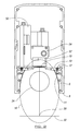
- FIG. 1 is a perspective view of a curing assembly in accordance with the invention
- FIG. 2 is an end view of the curing assembly of FIG. 1 ;
- FIG. 3 is a plan view of an LED array suitable for use in the assembly of FIG. 1 ,
- FIG. 4 is a plan view of another LED array suitable for use in the assembly of FIG. 1 .
- FIGS. 5 to 7 are ray diagrams illustrating the operation of the assembly of FIG. 1 .
- the curing assembly 2 comprises a reflector 4 preferably made of extruded aluminium and formed of two reflector elements 6 each secured in place between a flange 8 and a support 10 by bolts 12 .
- the reflector 4 provides a reflective surface 14 which in the form illustrated in FIG. 2 is elliptical.
- the full ellipse is show in dotted outline at 16 .
- the ellipse 16 has two focal points, an upper focal point at which an LED array 18 is positioned and a lower focal point 20 .
- the assembly 2 includes a substrate support which positions a substrate at the location indicated by line 22 which extends through the lower focal point 20 .
- the substrate support could be separate from the assembly and could be, for example, the curved impression cylinder of a printing press.
- a lens 24 is supported by end plates 26 between the LED array 18 and the substrate support position 22 .
- the lens 24 is shown in the figures as a cylindrical rod but could take other forms including in particular a rod having a semicircular cross-section arranged with the curved surface facing towards or away from the LED array 18 .
- a further alternative is a lens which is ground or otherwise shaped to make it convergent.
- the lens 24 is arranged such that its focal point coincides with the lower focal point 20 of the ellipse 16 .
- FIG. 3 One preferred form for the LED array 18 is illustrated in FIG. 3 .
- This has square LEDs 28 mounted on a circuit board 30 .
- the LEDs 28 have a width 32 and a depth 34 of 1.07 mm.
- the longitudinal pitch 38 is 2.10 mm whilst the lateral pitch 40 is 1.70 mm.
- the LEDs 28 in the regions 42 are arranged in staggered rows.
- the transverse pitch 40 remains 1.7 mm but the longitudinal pitch 46 is increased to 2.6 mm.
- the LEDs 28 in the central region 44 are reoriented by 45° with respect to the other LEDs 28 and the space in between them is slightly wider to allow for circuit tracks to be laid.
- the packing density of the LEDS 28 in the outer rows 36 is 31% whilst the packing density in the regions 42 is 26%.
- the close packing of the LEDs 28 in the rows 36 compensates for the drop off which is found to occur in radiation intensity at the edge regions of LED arrays.
- the increased spacing of the LEDs 28 in the intermediate and central regions 42 , 44 improves heat transfer and reduces the effect of heat from one die on adjacent dies.
- the rotation and spacing of the LEDs 28 in the central region 44 also improves heat transfer in this region and, as noted, allows for circuit tracks to be laid.
- FIG. 4 illustrates another preferred form for the LED array 18 .
- the LEDs 28 are square and 1.07 ⁇ 1.07 mm.
- the longitudinal pitch 38 is 2.10 mm in the three outer row 36 whilst the lateral pitch 40 in those rows 36 is 1.45 mm.
- the LEDs 28 between the outer rows 36 are gradually spread out to a longitudinal pitch 48 of 2.6 mm.
- the packing density in the outer rows 36 is 38% whilst the packing density therebetween is 32%.
- the embodiment of FIG. 4 which is more closely packed than that of FIG. 3 is possible with a more thermally conductive circuit board.
- FIG. 3 there are 192 LEDs 28 on a board 30 with a length L of 60.00 mm and a width W of 19.70 mm whilst in the embodiment of FIG. 4 there are 200 LEDs 28 on a board 30 with a length L of 60.00 mm and a width W of 19.70 mm.
- FIG. 1 there may be multiple arrays 18 , four in the illustrated embodiment, one of which is hidden from view.
- the array or arrays 18 are powered and controlled via a control driver 50 .
- the LEDs 18 generate significant heat and cooling is therefore required. In the illustrated embodiment this is provided by a water cooled copper block 52 which is in thermal contact with a manifold 54 provided with passages for circulation of cooling water.
- FIGS. 5 to 7 show the overall profile of the reflective surface 14 .
- the reflective surface 14 is shown in FIGS. 5 to 7 as a series of flat regions angled towards each other but this is for illustrative purposes only.
- FIG. 5 illustrates the path of the UV light from the reflective surface 14 alone whilst FIG. 6 illustrates the path of the UV light through the lens 24 alone i.e. without any reflection from the reflective surface 14 .
- the reflective surface 14 is arranged such that the rays combine at the substrate support position 22 .
- FIG. 6 shows that the effect of the lens is to generate a column of high intensity radiation.
- FIG. 7 illustrates the path of the UV radiation with the combination of the reflective surface 14 and lens 24 of the assembly 2 .
- the result of that combination is high intensity and efficiency even when the substrate support position 22 is at a significant distance from the LED array 18 .
- the reflective surface 14 is arranged to maximise reflection of the rays and to minimise the quantity of reflective radiation which passes between the lens 24 and the array 18 .
- the lens 24 is in the form of a cylindrical rod. This produces very satisfactory results but even better focussing is possible with a shaped lens 24 although this is at a cost.
- the assembly 2 allows use of UV LEDs where the radiation needs to be transmitted over significant distances such as 30 to 50 mm. This is achieved with an assembly which is compact. The design enables even and high UV intensity output.
Landscapes
- Engineering & Computer Science (AREA)
- General Engineering & Computer Science (AREA)
- Mechanical Engineering (AREA)
- Health & Medical Sciences (AREA)
- Toxicology (AREA)
- General Health & Medical Sciences (AREA)
- Microbiology (AREA)
- Life Sciences & Earth Sciences (AREA)
- Physics & Mathematics (AREA)
- Plasma & Fusion (AREA)
- Led Device Packages (AREA)
- Heating, Cooling, Or Curing Plastics Or The Like In General (AREA)
- Non-Portable Lighting Devices Or Systems Thereof (AREA)
- Microelectronics & Electronic Packaging (AREA)
- Optics & Photonics (AREA)
Applications Claiming Priority (2)
| Application Number | Priority Date | Filing Date | Title |
|---|---|---|---|
| GB1009063.7 | 2010-05-28 | ||
| GB1009063A GB2480693A (en) | 2010-05-28 | 2010-05-28 | Ultra violet light emitting diode curing assembly |
Publications (2)
| Publication Number | Publication Date |
|---|---|
| US20110290179A1 US20110290179A1 (en) | 2011-12-01 |
| US9018600B2 true US9018600B2 (en) | 2015-04-28 |
Family
ID=42371236
Family Applications (1)
| Application Number | Title | Priority Date | Filing Date |
|---|---|---|---|
| US13/116,067 Active 2032-05-12 US9018600B2 (en) | 2010-05-28 | 2011-05-26 | UV LED curing assembly |
Country Status (5)
| Country | Link |
|---|---|
| US (1) | US9018600B2 (enExample) |
| EP (1) | EP2390102B1 (enExample) |
| JP (1) | JP2011253808A (enExample) |
| CN (1) | CN102263096A (enExample) |
| GB (1) | GB2480693A (enExample) |
Cited By (2)
| Publication number | Priority date | Publication date | Assignee | Title |
|---|---|---|---|---|
| US20170009961A1 (en) * | 2015-07-08 | 2017-01-12 | Air Motion Systems, Inc. | Led module |
| US10641461B2 (en) * | 2017-07-07 | 2020-05-05 | Hoya Candeo Optronics Corporation | Light illuminating apparatus |
Families Citing this family (29)
| Publication number | Priority date | Publication date | Assignee | Title |
|---|---|---|---|---|
| US9022545B2 (en) * | 2012-03-08 | 2015-05-05 | Seiko Epson Corporation | Printing apparatus for irradiating UV light on ink ejected on medium and printing method for irradiating UV light on ink ejected on medium |
| JP5591305B2 (ja) * | 2012-10-30 | 2014-09-17 | 株式会社トクヤマ | 紫外線発光モジュール及び紫外線照射装置 |
| EP2765000A1 (de) | 2013-02-12 | 2014-08-13 | Farbwerke Herkula St. Vith S.A. | Härtung einer auf einem Substrat angeordneten Maserdruckbeschichtung |
| KR101312094B1 (ko) | 2013-04-18 | 2013-09-25 | 유버 주식회사 | Uv 엘이디를 이용하는 uv 경화장치 |
| JP6198465B2 (ja) * | 2013-05-28 | 2017-09-20 | 株式会社ミマキエンジニアリング | インクジェット記録装置 |
| CN103406246A (zh) * | 2013-07-11 | 2013-11-27 | 东莞科视自动化科技有限公司 | 一种面阵光源错位排列的平行光固化设备及其固化方法 |
| KR101376643B1 (ko) * | 2013-08-02 | 2014-03-25 | 유버 주식회사 | Uv 엘이디 모듈 및 이를 포함하는 uv 경화장치 |
| NL2011351C2 (nl) * | 2013-08-28 | 2015-05-26 | Codan B V | Reflectiemateriaal, halffabrikaat, reflector, werkwijze en gebruik daarvan. |
| JP6187081B2 (ja) * | 2013-09-19 | 2017-08-30 | 岩崎電気株式会社 | 照射ユニット |
| CN103568544A (zh) * | 2013-11-20 | 2014-02-12 | 北京慧眼智行科技有限公司 | 一种固化光学系统以及印刷设备 |
| WO2015112454A1 (en) * | 2014-01-21 | 2015-07-30 | Kateeva, Inc. | Apparatus and techniques for electronic device encapsulation |
| CN103939769B (zh) * | 2014-03-27 | 2016-01-20 | 西安精密印刷机械研究院有限公司 | 紫外光固化灯箱 |
| USD758324S1 (en) * | 2015-01-28 | 2016-06-07 | Phoseon Technology, Inc. | Controller box |
| KR101558275B1 (ko) | 2015-04-22 | 2015-10-15 | 유버 주식회사 | 자외선 led 모듈 및 이를 구비한 자외선 경화장치 |
| US10180248B2 (en) | 2015-09-02 | 2019-01-15 | ProPhotonix Limited | LED lamp with sensing capabilities |
| CN105398205B (zh) * | 2015-12-23 | 2017-12-12 | 青岛莱伊迪光电科技有限公司 | 一种led uv印刷固化装置 |
| JP6379118B2 (ja) * | 2016-01-10 | 2018-08-22 | Hoya Candeo Optronics株式会社 | 光照射装置 |
| DE112017002035T5 (de) * | 2016-04-15 | 2019-02-28 | Phoseon Technology, Inc. | Verfahren und System für die Emission von und das Härten mittels Strahlung mit geringer Breite |
| KR101808419B1 (ko) | 2016-04-21 | 2017-12-14 | 이훈 | 냉각부 및 광학격벽을 포함하는 led 광원을 이용한 스캔 방식의 노광장치 |
| CN106004083B (zh) * | 2016-05-26 | 2017-12-15 | 北京印刷学院 | 标签印刷机的反光倍增紫外线固化装置 |
| EP3281915B1 (en) | 2016-08-10 | 2019-02-20 | Umicore | Precursors for lithium transition metal oxide cathode materials for rechargeable batteries |
| JP6660317B2 (ja) * | 2017-01-31 | 2020-03-11 | Hoya Candeo Optronics株式会社 | 光照射装置 |
| RU2655162C1 (ru) * | 2017-08-18 | 2018-05-24 | Анатолий Николаевич Щелканов | Излучатель ультрафиолетовой светодиодной сушки для офсетной, листовой и ролевой печати (варианты) |
| CN109080259B (zh) * | 2018-07-31 | 2020-07-24 | 珠海迈时光电科技有限公司 | 一种uvled固化光源系统及其设计方法 |
| DE102018221729A1 (de) | 2018-12-14 | 2020-06-18 | Heraeus Noblelight Gmbh | Leuchte zum bestrahlen eines targets |
| CN109894334B (zh) * | 2019-04-04 | 2023-12-15 | 江阴天人工业技术服务有限公司 | 一种大功率uv led固化设备 |
| DE102020123695A1 (de) * | 2019-09-25 | 2021-03-25 | Heidelberger Druckmaschinen Aktiengesellschaft | Vorrichtung zum Bestrahlen eines Fluids auf einem Bedruckstoff |
| CN113695204B (zh) * | 2020-05-21 | 2022-10-18 | 长鑫存储技术有限公司 | 膜层固化装置 |
| CN117960543A (zh) * | 2024-02-05 | 2024-05-03 | 合肥国轩高科动力能源有限公司 | 一种uv固化光源模块 |
Citations (35)
| Publication number | Priority date | Publication date | Assignee | Title |
|---|---|---|---|---|
| US3573456A (en) * | 1967-07-26 | 1971-04-06 | Opto Mechanisms Inc | High resolution projection means for printing micro circuits on photoresist material |
| US5091915A (en) * | 1989-12-25 | 1992-02-25 | Mitsubishi Denki K.K. | Semiconductor laser excited solid laser device |
| WO1996028302A1 (en) | 1995-03-15 | 1996-09-19 | Mathiesen, Neils, Lang | A method for activating photoinitiators in photosensitive substrates and an apparatus for curing such substrates |
| US5826643A (en) * | 1996-06-07 | 1998-10-27 | International Business Machines Corporation | Method of cooling electronic devices using a tube in plate heat sink |
| US5973331A (en) * | 1996-08-02 | 1999-10-26 | Nordson Corporation | Lamp assembly |
| US6276822B1 (en) * | 1998-02-20 | 2001-08-21 | Yerchanik Bedrosian | Method of replacing a conventional vehicle light bulb with a light-emitting diode array |
| GB2360084A (en) | 2000-03-08 | 2001-09-12 | Nordson Corp | Shuttered ultra-violet/ infra-red lamp |
| US6469322B1 (en) * | 1998-02-06 | 2002-10-22 | General Electric Company | Green emitting phosphor for use in UV light emitting diodes |
| USD470255S1 (en) * | 2002-04-25 | 2003-02-11 | Pervaiz Lodhie | LED light bulb |
| US20040008475A1 (en) * | 2001-09-07 | 2004-01-15 | Shigeo Ohashi | Electronic apparatus |
| US6683421B1 (en) | 2001-01-25 | 2004-01-27 | Exfo Photonic Solutions Inc. | Addressable semiconductor array light source for localized radiation delivery |
| US20040075065A1 (en) * | 2003-06-11 | 2004-04-22 | Paul Spivak | UV LED light projection method and apparatus |
| US20040090794A1 (en) | 2002-11-08 | 2004-05-13 | Ollett Scott H. | High intensity photocuring system |
| US20040114367A1 (en) * | 2002-12-13 | 2004-06-17 | Jui-Tuan Li | Light emitting diode light bulb |
| US20040135159A1 (en) * | 2003-01-09 | 2004-07-15 | Siegel Stephen B. | Light emitting apparatus and method for curing inks, coatings and adhesives |
| US20050042390A1 (en) * | 2003-01-09 | 2005-02-24 | Siegel Stephen B. | Rotary UV curing method and apparatus |
| US20050062830A1 (en) | 2003-09-22 | 2005-03-24 | Fuji Photo Film Co., Ltd. | Light irradiating unit and optical fixing unit |
| EP1520718A1 (en) | 2003-09-30 | 2005-04-06 | Konica Minolta Medical & Graphic, Inc. | inkjet recording apparatus |
| GB2407371A (en) | 2001-02-27 | 2005-04-27 | Nordson Corp | A lamp assembly with additional reflectors to reduce the angular spread of radiation |
| US20050087768A1 (en) * | 2003-10-27 | 2005-04-28 | Atlas Material Testing Technology Gmbh | UV light-emitting diodes as a radiation source in a device for the artificial weathering of samples |
| US20050174769A1 (en) * | 2003-02-20 | 2005-08-11 | Gao Yong | LED light bulb and its application in a desk lamp |
| US20050196720A1 (en) * | 2000-03-08 | 2005-09-08 | Tir Systems Ltd. | Light emitting diode light source for curing dental composites |
| US20050212404A1 (en) * | 2004-03-24 | 2005-09-29 | Wen-Ho Chen | White light LED assembly |
| US20050222295A1 (en) * | 2003-01-09 | 2005-10-06 | Con-Trol-Cure, Inc. | UV Curing System and Process with Increased Light Intensity |
| US20050280683A1 (en) * | 2005-09-20 | 2005-12-22 | Custer Eric J | Ultraviolet light-emitting diode device |
| US20060291245A1 (en) * | 2003-12-10 | 2006-12-28 | Okaya Electric Industries Co., Ltd. | Indicator lamp |
| US20070024191A1 (en) * | 2005-07-27 | 2007-02-01 | Lung-Chien Chen | White light emitting diode using phosphor excitation |
| US20070159849A1 (en) * | 2006-01-06 | 2007-07-12 | Asagicreate Co., Ltd. | Surface light source and electrically illuminated signboard |
| WO2007096824A2 (en) | 2006-02-24 | 2007-08-30 | Yongqian Liu | Led curing light having fresnel lenses |
| USD553266S1 (en) * | 2004-10-08 | 2007-10-16 | Lighting Science Group Corporation | LED light bulb |
| US20080280227A1 (en) * | 2007-05-08 | 2008-11-13 | Wolfgang Sievers | Exposing printing plates using light emitting diodes |
| US20080315132A1 (en) * | 2004-03-29 | 2008-12-25 | Platsch Hans G | Flat Uv Light Source |
| US20090002669A1 (en) * | 2007-06-29 | 2009-01-01 | Optical Associates, Inc. | Ultraviolet light-emitting diode exposure apparatus for microfabrication |
| US20090034236A1 (en) * | 2007-07-30 | 2009-02-05 | David Isidore Reuben | Shoe With Ultraviolet LED Irradiated Photocatalyst Coated Surfaces. |
| US20090201368A1 (en) * | 2006-06-14 | 2009-08-13 | Pilkington Group Limited | Glazing inspection |
Family Cites Families (7)
| Publication number | Priority date | Publication date | Assignee | Title |
|---|---|---|---|---|
| JPH0233466U (enExample) * | 1988-08-26 | 1990-03-02 | ||
| JPH071804B2 (ja) * | 1989-02-15 | 1995-01-11 | シャープ株式会社 | 発光素子アレイ光源 |
| DE102006002275A1 (de) * | 2005-01-19 | 2006-07-20 | Osram Opto Semiconductors Gmbh | Beleuchtungseinrichtung |
| JP2007109945A (ja) * | 2005-10-14 | 2007-04-26 | Fujifilm Holdings Corp | 光源 |
| JP4108734B1 (ja) * | 2007-03-16 | 2008-06-25 | 株式会社モモ・アライアンス | 電気的接続に係る接続構造体、及び照明装置 |
| JP5208597B2 (ja) * | 2008-07-01 | 2013-06-12 | 富士フイルム株式会社 | 照明装置、撮像装置 |
| JP2010103687A (ja) * | 2008-10-22 | 2010-05-06 | Sanyo Electric Co Ltd | 線状照明装置及び画像読取装置 |
-
2010
- 2010-05-28 GB GB1009063A patent/GB2480693A/en not_active Withdrawn
-
2011
- 2011-05-20 JP JP2011113792A patent/JP2011253808A/ja active Pending
- 2011-05-25 EP EP11167418.0A patent/EP2390102B1/en active Active
- 2011-05-26 US US13/116,067 patent/US9018600B2/en active Active
- 2011-05-26 CN CN2011101378540A patent/CN102263096A/zh active Pending
Patent Citations (36)
| Publication number | Priority date | Publication date | Assignee | Title |
|---|---|---|---|---|
| US3573456A (en) * | 1967-07-26 | 1971-04-06 | Opto Mechanisms Inc | High resolution projection means for printing micro circuits on photoresist material |
| US5091915A (en) * | 1989-12-25 | 1992-02-25 | Mitsubishi Denki K.K. | Semiconductor laser excited solid laser device |
| WO1996028302A1 (en) | 1995-03-15 | 1996-09-19 | Mathiesen, Neils, Lang | A method for activating photoinitiators in photosensitive substrates and an apparatus for curing such substrates |
| US5826643A (en) * | 1996-06-07 | 1998-10-27 | International Business Machines Corporation | Method of cooling electronic devices using a tube in plate heat sink |
| US5973331A (en) * | 1996-08-02 | 1999-10-26 | Nordson Corporation | Lamp assembly |
| US6469322B1 (en) * | 1998-02-06 | 2002-10-22 | General Electric Company | Green emitting phosphor for use in UV light emitting diodes |
| US6276822B1 (en) * | 1998-02-20 | 2001-08-21 | Yerchanik Bedrosian | Method of replacing a conventional vehicle light bulb with a light-emitting diode array |
| GB2360084A (en) | 2000-03-08 | 2001-09-12 | Nordson Corp | Shuttered ultra-violet/ infra-red lamp |
| US20050196720A1 (en) * | 2000-03-08 | 2005-09-08 | Tir Systems Ltd. | Light emitting diode light source for curing dental composites |
| US6683421B1 (en) | 2001-01-25 | 2004-01-27 | Exfo Photonic Solutions Inc. | Addressable semiconductor array light source for localized radiation delivery |
| GB2407371A (en) | 2001-02-27 | 2005-04-27 | Nordson Corp | A lamp assembly with additional reflectors to reduce the angular spread of radiation |
| US20040008475A1 (en) * | 2001-09-07 | 2004-01-15 | Shigeo Ohashi | Electronic apparatus |
| USD470255S1 (en) * | 2002-04-25 | 2003-02-11 | Pervaiz Lodhie | LED light bulb |
| US20040090794A1 (en) | 2002-11-08 | 2004-05-13 | Ollett Scott H. | High intensity photocuring system |
| US20040114367A1 (en) * | 2002-12-13 | 2004-06-17 | Jui-Tuan Li | Light emitting diode light bulb |
| US20040135159A1 (en) * | 2003-01-09 | 2004-07-15 | Siegel Stephen B. | Light emitting apparatus and method for curing inks, coatings and adhesives |
| US20050042390A1 (en) * | 2003-01-09 | 2005-02-24 | Siegel Stephen B. | Rotary UV curing method and apparatus |
| US20050222295A1 (en) * | 2003-01-09 | 2005-10-06 | Con-Trol-Cure, Inc. | UV Curing System and Process with Increased Light Intensity |
| US20050174769A1 (en) * | 2003-02-20 | 2005-08-11 | Gao Yong | LED light bulb and its application in a desk lamp |
| US20040075065A1 (en) * | 2003-06-11 | 2004-04-22 | Paul Spivak | UV LED light projection method and apparatus |
| US20050062830A1 (en) | 2003-09-22 | 2005-03-24 | Fuji Photo Film Co., Ltd. | Light irradiating unit and optical fixing unit |
| EP1520718A1 (en) | 2003-09-30 | 2005-04-06 | Konica Minolta Medical & Graphic, Inc. | inkjet recording apparatus |
| US20050087768A1 (en) * | 2003-10-27 | 2005-04-28 | Atlas Material Testing Technology Gmbh | UV light-emitting diodes as a radiation source in a device for the artificial weathering of samples |
| US20060291245A1 (en) * | 2003-12-10 | 2006-12-28 | Okaya Electric Industries Co., Ltd. | Indicator lamp |
| US20090052190A1 (en) * | 2003-12-10 | 2009-02-26 | Toshio Shimada | Indicator lamp having a converging lens |
| US20050212404A1 (en) * | 2004-03-24 | 2005-09-29 | Wen-Ho Chen | White light LED assembly |
| US20080315132A1 (en) * | 2004-03-29 | 2008-12-25 | Platsch Hans G | Flat Uv Light Source |
| USD553266S1 (en) * | 2004-10-08 | 2007-10-16 | Lighting Science Group Corporation | LED light bulb |
| US20070024191A1 (en) * | 2005-07-27 | 2007-02-01 | Lung-Chien Chen | White light emitting diode using phosphor excitation |
| US20050280683A1 (en) * | 2005-09-20 | 2005-12-22 | Custer Eric J | Ultraviolet light-emitting diode device |
| US20070159849A1 (en) * | 2006-01-06 | 2007-07-12 | Asagicreate Co., Ltd. | Surface light source and electrically illuminated signboard |
| WO2007096824A2 (en) | 2006-02-24 | 2007-08-30 | Yongqian Liu | Led curing light having fresnel lenses |
| US20090201368A1 (en) * | 2006-06-14 | 2009-08-13 | Pilkington Group Limited | Glazing inspection |
| US20080280227A1 (en) * | 2007-05-08 | 2008-11-13 | Wolfgang Sievers | Exposing printing plates using light emitting diodes |
| US20090002669A1 (en) * | 2007-06-29 | 2009-01-01 | Optical Associates, Inc. | Ultraviolet light-emitting diode exposure apparatus for microfabrication |
| US20090034236A1 (en) * | 2007-07-30 | 2009-02-05 | David Isidore Reuben | Shoe With Ultraviolet LED Irradiated Photocatalyst Coated Surfaces. |
Cited By (3)
| Publication number | Priority date | Publication date | Assignee | Title |
|---|---|---|---|---|
| US20170009961A1 (en) * | 2015-07-08 | 2017-01-12 | Air Motion Systems, Inc. | Led module |
| US10217919B2 (en) * | 2015-07-08 | 2019-02-26 | Air Motion Systems, Inc. | LED module |
| US10641461B2 (en) * | 2017-07-07 | 2020-05-05 | Hoya Candeo Optronics Corporation | Light illuminating apparatus |
Also Published As
| Publication number | Publication date |
|---|---|
| JP2011253808A (ja) | 2011-12-15 |
| EP2390102A3 (en) | 2012-03-07 |
| EP2390102A2 (en) | 2011-11-30 |
| GB2480693A (en) | 2011-11-30 |
| GB201009063D0 (en) | 2010-07-14 |
| CN102263096A (zh) | 2011-11-30 |
| EP2390102B1 (en) | 2014-02-12 |
| US20110290179A1 (en) | 2011-12-01 |
Similar Documents
| Publication | Publication Date | Title |
|---|---|---|
| US9018600B2 (en) | UV LED curing assembly | |
| US8869419B2 (en) | Efficient irradiation system using curved reflective surfaces | |
| KR102700861B1 (ko) | 방사선 경화를 위한 uv 조사 유닛 | |
| CN109973840B (zh) | 具有led和圆柱形透镜的发光体 | |
| KR102304706B1 (ko) | 광 조사장치 | |
| KR200485222Y1 (ko) | Led 어레이로부터 광의 각도 확산을 감소시키기 위한 선형 프레스넬 옵틱 | |
| KR101748016B1 (ko) | 반사기를 갖춘 조명 유닛 | |
| KR200484992Y1 (ko) | 개선되는 균일도 범위를 위한 led들의 에지 가중 간격 | |
| US20150076368A1 (en) | Efficient irradiation system using curved reflective surfaces | |
| US9033555B2 (en) | Wrap-around window for lighting module | |
| US20150076367A1 (en) | Efficient radiating system using curved reflective surfaces | |
| KR101728532B1 (ko) | Led 광원을 이용한 스캔 방식의 노광장치 | |
| KR20180126073A (ko) | 좁은 폭 방사를 통한 방출 및 경화를 위한 방법 및 시스템 | |
| JP7367024B2 (ja) | ターゲット照射用照明器具 | |
| KR102310905B1 (ko) | Uv led의 복사 에너지 제어 장치 | |
| HK40005603A (en) | Lamp with led and cylinder lens | |
| CN109469838B (zh) | 光照射装置 | |
| JP2010234729A (ja) | 紫外線照射装置 | |
| KR20150121512A (ko) | Led를 이용한 자외선 경화기 | |
| HK1204147B (zh) | 具有led和圆柱形透镜的发光体 |
Legal Events
| Date | Code | Title | Description |
|---|---|---|---|
| AS | Assignment |
Owner name: BALDWIN UV LIMITED, UNITED KINGDOM Free format text: ASSIGNMENT OF ASSIGNORS INTEREST;ASSIGNORS:STOWELL, QUINTON;ARMITAGE, DAVID;REEL/FRAME:026345/0106 Effective date: 20110526 |
|
| STCF | Information on status: patent grant |
Free format text: PATENTED CASE |
|
| MAFP | Maintenance fee payment |
Free format text: PAYMENT OF MAINTENANCE FEE, 4TH YEAR, LARGE ENTITY (ORIGINAL EVENT CODE: M1551); ENTITY STATUS OF PATENT OWNER: LARGE ENTITY Year of fee payment: 4 |
|
| MAFP | Maintenance fee payment |
Free format text: PAYMENT OF MAINTENANCE FEE, 8TH YEAR, LARGE ENTITY (ORIGINAL EVENT CODE: M1552); ENTITY STATUS OF PATENT OWNER: LARGE ENTITY Year of fee payment: 8 |