EP2390102A2 - UV LED Curing Assembly - Google Patents
UV LED Curing Assembly Download PDFInfo
- Publication number
- EP2390102A2 EP2390102A2 EP11167418A EP11167418A EP2390102A2 EP 2390102 A2 EP2390102 A2 EP 2390102A2 EP 11167418 A EP11167418 A EP 11167418A EP 11167418 A EP11167418 A EP 11167418A EP 2390102 A2 EP2390102 A2 EP 2390102A2
- Authority
- EP
- European Patent Office
- Prior art keywords
- leds
- curing assembly
- lens
- curing
- radiation
- Prior art date
- Legal status (The legal status is an assumption and is not a legal conclusion. Google has not performed a legal analysis and makes no representation as to the accuracy of the status listed.)
- Granted
Links
Images


Classifications
-
- B—PERFORMING OPERATIONS; TRANSPORTING
- B41—PRINTING; LINING MACHINES; TYPEWRITERS; STAMPS
- B41J—TYPEWRITERS; SELECTIVE PRINTING MECHANISMS, i.e. MECHANISMS PRINTING OTHERWISE THAN FROM A FORME; CORRECTION OF TYPOGRAPHICAL ERRORS
- B41J11/00—Devices or arrangements of selective printing mechanisms, e.g. ink-jet printers or thermal printers, for supporting or handling copy material in sheet or web form
- B41J11/0015—Devices or arrangements of selective printing mechanisms, e.g. ink-jet printers or thermal printers, for supporting or handling copy material in sheet or web form for treating before, during or after printing or for uniform coating or laminating the copy material before or after printing
- B41J11/002—Curing or drying the ink on the copy materials, e.g. by heating or irradiating
- B41J11/0021—Curing or drying the ink on the copy materials, e.g. by heating or irradiating using irradiation
- B41J11/00214—Curing or drying the ink on the copy materials, e.g. by heating or irradiating using irradiation using UV radiation
-
- B—PERFORMING OPERATIONS; TRANSPORTING
- B05—SPRAYING OR ATOMISING IN GENERAL; APPLYING FLUENT MATERIALS TO SURFACES, IN GENERAL
- B05D—PROCESSES FOR APPLYING FLUENT MATERIALS TO SURFACES, IN GENERAL
- B05D3/00—Pretreatment of surfaces to which liquids or other fluent materials are to be applied; After-treatment of applied coatings, e.g. intermediate treating of an applied coating preparatory to subsequent applications of liquids or other fluent materials
- B05D3/06—Pretreatment of surfaces to which liquids or other fluent materials are to be applied; After-treatment of applied coatings, e.g. intermediate treating of an applied coating preparatory to subsequent applications of liquids or other fluent materials by exposure to radiation
- B05D3/061—Pretreatment of surfaces to which liquids or other fluent materials are to be applied; After-treatment of applied coatings, e.g. intermediate treating of an applied coating preparatory to subsequent applications of liquids or other fluent materials by exposure to radiation using U.V.
- B05D3/065—After-treatment
- B05D3/067—Curing or cross-linking the coating
-
- B—PERFORMING OPERATIONS; TRANSPORTING
- B41—PRINTING; LINING MACHINES; TYPEWRITERS; STAMPS
- B41F—PRINTING MACHINES OR PRESSES
- B41F23/00—Devices for treating the surfaces of sheets, webs, or other articles in connection with printing
- B41F23/04—Devices for treating the surfaces of sheets, webs, or other articles in connection with printing by heat drying, by cooling, by applying powders
- B41F23/0403—Drying webs
- B41F23/0406—Drying webs by radiation
- B41F23/0409—Ultraviolet dryers
-
- B—PERFORMING OPERATIONS; TRANSPORTING
- B41—PRINTING; LINING MACHINES; TYPEWRITERS; STAMPS
- B41F—PRINTING MACHINES OR PRESSES
- B41F23/00—Devices for treating the surfaces of sheets, webs, or other articles in connection with printing
- B41F23/04—Devices for treating the surfaces of sheets, webs, or other articles in connection with printing by heat drying, by cooling, by applying powders
- B41F23/044—Drying sheets, e.g. between two printing stations
- B41F23/045—Drying sheets, e.g. between two printing stations by radiation
- B41F23/0453—Drying sheets, e.g. between two printing stations by radiation by ultraviolet dryers
-
- F—MECHANICAL ENGINEERING; LIGHTING; HEATING; WEAPONS; BLASTING
- F26—DRYING
- F26B—DRYING SOLID MATERIALS OR OBJECTS BY REMOVING LIQUID THEREFROM
- F26B3/00—Drying solid materials or objects by processes involving the application of heat
- F26B3/28—Drying solid materials or objects by processes involving the application of heat by radiation, e.g. from the sun
- F26B3/283—Drying solid materials or objects by processes involving the application of heat by radiation, e.g. from the sun in combination with convection
-
- F—MECHANICAL ENGINEERING; LIGHTING; HEATING; WEAPONS; BLASTING
- F41—WEAPONS
- F41G—WEAPON SIGHTS; AIMING
- F41G11/00—Details of sighting or aiming apparatus; Accessories
- F41G11/001—Means for mounting tubular or beam shaped sighting or aiming devices on firearms
- F41G11/003—Mountings with a dove tail element, e.g. "Picatinny rail systems"
Definitions
- This invention relates to curing assemblies such as are used in the printing and coating industry for the fast curing of inks and the like on a large variety of substrate materials.
- the substrate is moved in a path beneath an elongate radiation source so that a coating on the substrate is irradiated by radiation from the source to cure the coating in a continuous process.
- the substrate may be continuous or comprise multiple sheets which are fed past the source in succession.
- each lamp in an assembly with a reflector which includes a reflective surface partly surrounding the lamp for reflecting radiation therefrom onto the substrate.
- the reflective surface has a concave profile which is commonly elliptical or parabolic, the lamp being mounted on the symmetrical centre fine of the profile and adjacent the apex.
- the reflector increases the intensity of the radiation received by the curable coating.
- the penetration of the radiation into the coating is an important factor in curing and, whilst penetration varies with different colours and materials, the higher the intensity, the better the penetration.
- mercury lamps generate large amounts of heat and IR radiation which can damage the substrate being cured, for example by warping and/or distortion.
- a further disadvantage is the slow start up of mercury lamps which can take one to two minutes to reach the operating temperature.
- UV LEDs as the UV radiation source for curing applications since the performance of UV LEDs has increased to the point where they are a viable alternative to mercury lamps.
- UV LEDS themselves have problems, one of which is the ability to focus sufficient radiation onto the substrate being cured.
- the distance between the radiation source and substrate is in the range of 30 to 50 mm and some where the distance is 100 mm. Thus it is necessary that the radiation be provided effectively across a gap of at least 50 mm.
- the present invention provides a curing assembly comprising at least one array of UV LEDs, a reflector with an elongate reflective surface partly surrounding the array and having an opening for emission of radiation, towards a substrate supported in a position to receive radiation emitted through the opening for curing a coating thereon, and a lens between the array and the opening.
- the reflective surface has two focal points and the array is located at one focal point and the substrate support position at the other. This produces good focussing of radiation from the array onto the substrate support position.
- direct rays which are continually diverging do not come to the reflective surface focal point.
- the lens is provided for these direct rays and preferably it and the reflective surface have a common focal point at the substrate support position.
- the reflective surface is shaped and positioned to maximise reflection of radiation which does not pass through the lens and to minimise the amount of radiation which is reflected back onto the lens.
- the reflective surface can be designed to meet these criteria in the form of an ellipse or an arc.
- the lens may be a cylindrical rod.
- the lens may be a rod of semicircular cross-section which may be arranged with the curved face adjacent the array.
- the rod is preferably formed of quartz due to its high refractive index and good transmission of UV light. With both alternatives the lens is simple in form and cheap to provide.
- the lens may be a convergent lens arranged to focus radiation at the substrate support position.
- the lens will be ground or otherwise shaped to function as in a pair of spectacles. Whilst this is a more expensive option, it can produce great efficiency of curing.
- the LEDs may be arranged in a pattern with LEDs in outer regions being closer together than the other LEDs. There may be a central region where the LEDs are rotated relative the other LEDs, preferably by 45 degrees, and/or the LEDs in the central region may be spaced further apart than the other LEDs.
- the outer regions may comprise two or more rows of LEDs and there may be an intermediate region between each outer region and the central region where the LEDs are arranged in staggered rows.
- UV LEDs One problem with the use of UV LEDs is overheating of the LEDs as they are driven at high current. Commonly the LEDs are only 25% efficient with heat accounting for the other 75%. Another is the inevitable UV drop off that occurs at outer regions of the array, which is often referred to as the "end effect”.
- the preferred pattern overcomes these problems.
- the closer positioning of the LEDs or dies in the outer regions offsets the "end effect". Making the spacing of the other LEDs higher leads to better thermal heat transfer and a reduced heat effect from one die on adjacent dies.
- the rotation and spacing of the centrally positioned LEDs allows for circuit tracks to be laid and provides for maximum heat transfer efficiency in the centre.
- the "pitch” is the distance between the centres of adjacent LEDs.
- the “pitch area” is calculated by multiplying the pitch in the longitudinal direction of the board by the pitch in the width wise direction.
- the "area of dies” is calculated by multiplying the die width and die length which with square dies will be the same.
- the LEDs are mounted on a circuit board which may be water cooled.
- Water cooling can be achieved by use of one or more blocks of material with good heat transfer properties, such as copper, in conjunction with a manifold through which water is continuously circulated.
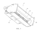
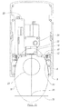
- the curing assembly 2 comprises a reflector 4 preferably made of extruded aluminium and formed of two reflector elements 6 each secured in place between a flange 8 and a support 10 by bolts 12.
- the reflector 4 provides a reflective surface 14 which in the form illustrated in Figure 2 is elliptical.
- the full ellipse is show in dotted outline at 16.
- the ellipse 16 has two focal points, an upper focal point at which an LED array 18 is positioned and a lower focal point 20.
- the assembly 2 includes a substrate support which positions a substrate at the location indicated by line 22 which extends through the lower focal point 20.
- the substrate support could be separate from the assembly and could be, for example, the curved impression cylinder of a printing press.
- a lens 24 is supported by end plates 26 between the LED array 18 and the substrate support position 22.
- the lens 24 is shown in the figures as a cylindrical rod but could take other forms including in particular a rod having a semicircular cross-section arranged with the curved surface facing towards or away from the LED array 18.
- a further alternative is a lens which is ground or otherwise shaped to make it convergent.
- the lens 24 is arranged such that its focal point coincides with the lower focal point 20 of the ellipse 16.
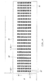
- FIG. 3 One preferred form for the LED array 18 is illustrated in Figure 3 .
- This has square LEDs 28 mounted on a circuit board 30. in the embodiment of Figure 3 the LEDs 28 have a width 32 and a depth 34 of 1.07 mm.
- the longitudinal pitch 38 is 2.10 mm whilst the lateral pitch 40 is 1.70 mm.
- the LEDs 28 in the regions 42 are arranged in staggered rows.
- the transverse pitch 40 remains 1.7 mm but the longitudinal pitch 46 is increased to 2.6 mm.
- the LEDs 28 in the central region 44 are reoriented by 45° with respect to the other LEDs 28 and the space in between them is slightly wider to allow for circuit tracks to be laid.
- the parking density of the LEDS 28 in the outer rows 36 is 31% whilst the packing density in the regions 42 is 26%.
- the close packing of the LEDs 28 in the rows 36 compensates for the drop off which is found to occur in radiation intensity at the edge regions of LED arrays.
- the increased spacing of the LEDs 28 in the intermediate and central regions 42, 44 improves heat transfer and reduces the effect of heat from one die on adjacent dies.
- the rotation and spacing of the LEDs 28 in the central region 44 also improves heat transfer in this region and, as noted, allows for circuit tracks to be laid.
- Figure 4 illustrates another preferred form for the LED array 18.
- the LEDs 28 are square and 1.07 x 1.07 mm.
- the longitudinal pitch 38 is 2.10 mm in the three outer row 36 whilst the lateral pitch 40 in those rows 36 is 1.45 mm.
- the LEDs 28 between the outer rows 36 are gradually spread out to a longitudinal pitch 48 of 2.6 mm.
- the packing density in the outer rows 36 is 38% whilst the packing density therebetween is 32%.
- the embodiment of Figure 4 which is more closely packed than that of Figure 3 is possible with a more thermally conductive circuit board.
- FIG. 1 there may be multiple arrays 18, four in the illustrated embodiment, one of which is hidden from view.
- the array or arrays 18 are powered and controlled via a control driver 50.
- the LEDs 18 generate significant heat and cooling is therefore required. In the illustrated embodiment this is provided by a water cooled copper block 52 which is in thermal contact with a manifold 54 provided with passages for circulation of cooling water.
- FIGS 5 to 7 show the overall profile of the reflective surface 14.
- the reflective surface 14 is shown in Figures 5 to 7 as a series of flat regions angled towards each other but this is for illustrative purposes only.
- the reflective surface 14 is arranged to maximise reflection of the rays and to minimise the quantity of reflective radiation which passes between the lens 24 and the array 18.
- the lens 24 is in the form of a cylindrical rod. This produces very satisfactory results but even better focussing is possible with a shaped lens 24 although this is at a cost.
- the assembly 2 allows use of UV LEDs where the radiation needs to be transmitted over significant distances such as 30 to 50 mm. This is achieved with an assembly which is compact. The design enables even and high UV intensity output.
Landscapes
- Engineering & Computer Science (AREA)
- General Engineering & Computer Science (AREA)
- Mechanical Engineering (AREA)
- Health & Medical Sciences (AREA)
- Toxicology (AREA)
- General Health & Medical Sciences (AREA)
- Microbiology (AREA)
- Life Sciences & Earth Sciences (AREA)
- Physics & Mathematics (AREA)
- Plasma & Fusion (AREA)
- Led Device Packages (AREA)
- Heating, Cooling, Or Curing Plastics Or The Like In General (AREA)
- Optics & Photonics (AREA)
- Microelectronics & Electronic Packaging (AREA)
- Non-Portable Lighting Devices Or Systems Thereof (AREA)
Abstract
Description
- This invention relates to curing assemblies such as are used in the printing and coating industry for the fast curing of inks and the like on a large variety of substrate materials. During the curing process, the substrate is moved in a path beneath an elongate radiation source so that a coating on the substrate is irradiated by radiation from the source to cure the coating in a continuous process. The substrate may be continuous or comprise multiple sheets which are fed past the source in succession.
- It is well known to cure inks on the substrate by application of ultra-violet radiation from one or more medium-pressure mercury vapour ultra-violet lamps. It is also well known to provide each lamp in an assembly with a reflector which includes a reflective surface partly surrounding the lamp for reflecting radiation therefrom onto the substrate. The reflective surface has a concave profile which is commonly elliptical or parabolic, the lamp being mounted on the symmetrical centre fine of the profile and adjacent the apex.
- The reflector increases the intensity of the radiation received by the curable coating. The penetration of the radiation into the coating is an important factor in curing and, whilst penetration varies with different colours and materials, the higher the intensity, the better the penetration.
- One drawback of mercury lamps is that they generate large amounts of heat and IR radiation which can damage the substrate being cured, for example by warping and/or distortion. A further disadvantage is the slow start up of mercury lamps which can take one to two minutes to reach the operating temperature. As a consequence of recent years there has been great interest in using UV LEDs as the UV radiation source for curing applications since the performance of UV LEDs has increased to the point where they are a viable alternative to mercury lamps.
- However, UV LEDS themselves have problems, one of which is the ability to focus sufficient radiation onto the substrate being cured. There are many printing machines in use where the distance between the radiation source and substrate is in the range of 30 to 50 mm and some where the distance is 100 mm. Thus it is necessary that the radiation be provided effectively across a gap of at least 50 mm.
- It is known to use a reflector with UV LEDs of a similar form to those employed with mercury lamps. However, this does not provide sufficient radiation intensity at large gaps such as 50 mm. Light intensity at a distance is also a problem with known systems where either the LEDs are provided with individual lenses, or the LEDs are arranged in a row and a lens provided for each row.
- The present invention provides a curing assembly comprising at least one array of UV LEDs, a reflector with an elongate reflective surface partly surrounding the array and having an opening for emission of radiation, towards a substrate supported in a position to receive radiation emitted through the opening for curing a coating thereon, and a lens between the array and the opening.
- It has been found that the combination of a reflector and a lens enables efficient generation of an intense beam of radiation even at high source-substrate distances. The combination makes for a very compact an efficient optical system.
- In one preferred embodiment the reflective surface has two focal points and the array is located at one focal point and the substrate support position at the other. This produces good focussing of radiation from the array onto the substrate support position. However, direct rays which are continually diverging do not come to the reflective surface focal point. The lens is provided for these direct rays and preferably it and the reflective surface have a common focal point at the substrate support position.
- The reflective surface is shaped and positioned to maximise reflection of radiation which does not pass through the lens and to minimise the amount of radiation which is reflected back onto the lens. The reflective surface can be designed to meet these criteria in the form of an ellipse or an arc.
- The lens may be a cylindrical rod. Alternatively the lens may be a rod of semicircular cross-section which may be arranged with the curved face adjacent the array. In either case the rod is preferably formed of quartz due to its high refractive index and good transmission of UV light. With both alternatives the lens is simple in form and cheap to provide.
- Alternatively the lens may be a convergent lens arranged to focus radiation at the substrate support position. The lens will be ground or otherwise shaped to function as in a pair of spectacles. Whilst this is a more expensive option, it can produce great efficiency of curing.
- The LEDs may be arranged in a pattern with LEDs in outer regions being closer together than the other LEDs. There may be a central region where the LEDs are rotated relative the other LEDs, preferably by 45 degrees, and/or the LEDs in the central region may be spaced further apart than the other LEDs.
- In one embodiment the outer regions may comprise two or more rows of LEDs and there may be an intermediate region between each outer region and the central region where the LEDs are arranged in staggered rows.
- One problem with the use of UV LEDs is overheating of the LEDs as they are driven at high current. Commonly the LEDs are only 25% efficient with heat accounting for the other 75%. Another is the inevitable UV drop off that occurs at outer regions of the array, which is often referred to as the "end effect".
- The preferred pattern overcomes these problems. The closer positioning of the LEDs or dies in the outer regions offsets the "end effect". Making the spacing of the other LEDs higher leads to better thermal heat transfer and a reduced heat effect from one die on adjacent dies. The rotation and spacing of the centrally positioned LEDs allows for circuit tracks to be laid and provides for maximum heat transfer efficiency in the centre.
- The array pattern has a packing density which is between 15 to 60%, preferably between 20 to 38%, the packing density being defined as:

- The "pitch" is the distance between the centres of adjacent LEDs. The "pitch area" is calculated by multiplying the pitch in the longitudinal direction of the board by the pitch in the width wise direction. The "area of dies" is calculated by multiplying the die width and die length which with square dies will be the same.
- The LEDs are mounted on a circuit board which may be water cooled. Water cooling can be achieved by use of one or more blocks of material with good heat transfer properties, such as copper, in conjunction with a manifold through which water is continuously circulated.
- The invention will now be further described by way of example with reference to the accompanying drawings in which:
-
Figure 1 is a perspective view of a curing assembly in accordance with the invention; -
Figure 2 is an end view of the curing assembly ofFigure 1 ; -
Figure 3 is a plan view of an LED array suitable for use in the assembly ofFigure 1 , -
Figure 4 is a plan view of another LED array suitable for use in the assembly ofFigure 1 , and -
Figures 5 to 7 are ray diagrams illustrating the operation of the assembly ofFigure 1 . - The curing assembly 2 comprises a reflector 4 preferably made of extruded aluminium and formed of two
reflector elements 6 each secured in place between a flange 8 and asupport 10 bybolts 12. The reflector 4 provides areflective surface 14 which in the form illustrated inFigure 2 is elliptical. The full ellipse is show in dotted outline at 16. Theellipse 16 has two focal points, an upper focal point at which anLED array 18 is positioned and a lowerfocal point 20. - The assembly 2 includes a substrate support which positions a substrate at the location indicated by
line 22 which extends through the lowerfocal point 20. Alternatively the substrate support could be separate from the assembly and could be, for example, the curved impression cylinder of a printing press. - A
lens 24 is supported byend plates 26 between theLED array 18 and thesubstrate support position 22. Thelens 24 is shown in the figures as a cylindrical rod but could take other forms including in particular a rod having a semicircular cross-section arranged with the curved surface facing towards or away from theLED array 18. A further alternative is a lens which is ground or otherwise shaped to make it convergent. - Whatever form the
lens 24 takes, it is arranged such that its focal point coincides with the lowerfocal point 20 of theellipse 16. - One preferred form for the
LED array 18 is illustrated inFigure 3 . This hassquare LEDs 28 mounted on acircuit board 30. in the embodiment ofFigure 3 theLEDs 28 have awidth 32 and adepth 34 of 1.07 mm. In the tworows 36 at each end of theboard 30 thelongitudinal pitch 38 is 2.10 mm whilst thelateral pitch 40 is 1.70 mm. There ars then tworegions 42 one on either side and separated by acentral region 44. TheLEDs 28 in theregions 42 are arranged in staggered rows. Thetransverse pitch 40 remains 1.7 mm but thelongitudinal pitch 46 is increased to 2.6 mm. TheLEDs 28 in thecentral region 44 are reoriented by 45° with respect to theother LEDs 28 and the space in between them is slightly wider to allow for circuit tracks to be laid. - The parking density of the
LEDS 28 in theouter rows 36 is 31% whilst the packing density in theregions 42 is 26%. - The close packing of the
LEDs 28 in therows 36 compensates for the drop off which is found to occur in radiation intensity at the edge regions of LED arrays. The increased spacing of theLEDs 28 in the intermediate andcentral regions LEDs 28 in thecentral region 44 also improves heat transfer in this region and, as noted, allows for circuit tracks to be laid. -
Figure 4 illustrates another preferred form for theLED array 18. As with that ofFigure 3 , theLEDs 28 are square and 1.07 x 1.07 mm. Thelongitudinal pitch 38 is 2.10 mm in the threeouter row 36 whilst thelateral pitch 40 in thoserows 36 is 1.45 mm. TheLEDs 28 between theouter rows 36 are gradually spread out to a longitudinal pitch 48 of 2.6 mm. The packing density in theouter rows 36 is 38% whilst the packing density therebetween is 32%. The embodiment ofFigure 4 which is more closely packed than that ofFigure 3 is possible with a more thermally conductive circuit board. - In the embodiment of
Figure 3 there are 192LEDS 28 on aboard 30 with a length L of 60.00 mm and a width W of 19.70 mm whilst in the embodiment ofFigure 4 there are 200LEDs 28 on aboard 30 with a length L of 60.00 mm and a width W of 19.70 mm. - As shown in
Figure 1 , there may bemultiple arrays 18, four in the illustrated embodiment, one of which is hidden from view. The array orarrays 18 are powered and controlled via acontrol driver 50. TheLEDs 18 generate significant heat and cooling is therefore required. In the illustrated embodiment this is provided by a water cooledcopper block 52 which is in thermal contact with a manifold 54 provided with passages for circulation of cooling water. - The operation of the combination of the
reflective surface 14 andlens 24 is illustrated byFigures 5 to 7 . These figures, likeFigure 2 , show the overall profile of thereflective surface 14. Thereflective surface 14 is shown inFigures 5 to 7 as a series of flat regions angled towards each other but this is for illustrative purposes only. - Figures illustrates the path of the UV light from the
reflective surface 14 alone whilstFigure 6 illustrates the path of the UV light through thelens 24 alone i.e. without any reflection from thereflective surface 14. AsFigure 5 illustrates, thereflective surface 14 is arranged such that the rays combine at thesubstrate support position 22.Figure 6 shows that the effect of the lens is to generate a column of high intensity radiation, -
Figure 7 illustrates the path of the UV radiation with the combination of thereflective surface 14 andlens 24 of the assembly 2. The result of that combination is high intensity and efficiency even when thesubstrate support position 22 is at a significant distance from theLED array 18. - The
reflective surface 14 is arranged to maximise reflection of the rays and to minimise the quantity of reflective radiation which passes between thelens 24 and thearray 18. - It has been found that an elliptical
reflective surface 14, as illustrated inFigure 2 , gives optimum results but that it is possible to achieve a high proportion of desired reflection, up to 95%, with an arcuate surface. - As discussed above the
lens 24 is in the form of a cylindrical rod. This produces very satisfactory results but even better focussing is possible with a shapedlens 24 although this is at a cost. - The assembly 2 allows use of UV LEDs where the radiation needs to be transmitted over significant distances such as 30 to 50 mm. This is achieved with an assembly which is compact. The design enables even and high UV intensity output.
Claims (15)
- A curing assembly comprising at least one array of UV LEDs, a reflector with an elongate reflective surface partly surrounding the array and having an opening for emission of radiation towards a substrate supported in a position to receive radiation emitted through the opening for curing a coating thereon, and a lens between the array and the opening.
- A curing assembly as claimed in claim 1 wherein the reflective surface has two focal points and the array is located at one focal point and the substrate support position at the other.
- A curing assembly as claimed in either claim 1 or claim 2 wherein the reflective surface and tens have a common focal point at the substrate support position.
- A curing assembly as claimed in any preceding claim wherein the reflective surface is shaped and positioned to maximise reflection of radiation which does not pass through the lens and to minimise the amount of radiation which is reflected back onto the lens.
- A curing assembly as claimed in any preceding claim wherein the lens is a cylindrical rod.
- A curing assembly as claimed in any one of claims 1 to 4 wherein the lens is a rod of semicircular cross-section.
- A curing assembly as claimed in either claim 5 or claim 6 wherein the rod is formed of quartz.
- A curing assembly as claimed in any one of claims 1 to 4 wherein the lens is a convergent lens arranged to focus radiation at the substrate support position.
- A curing assembly as claimed in any preceding claim wherein the LEDs are arranged in a pattern, the LEDs in outer regions being closer together than the other LEDs,
- A curing assembly as claimed in any preceding claim wherein the LEDs are arranged in a pattern including a central region where the LEDs are rotated relative to other LEDs.
- A curing assembly as claimed in claim 10 wherein the LEDs in the central region are rotated 46 degrees relative the other LEDs.
- A curing assembly as claimed in either claim 10 or claim 11 wherein the LEDs in the central region are spaced further apart than the other LEOs.
- A curing assembly as claimed in any preceding claim wherein the LEDs have a packing density of 15 to 50%, preferably 20 to 38%.
- A curing assembly as claimed in any preceding claim wherein the LEDs are mounted on a water cooled circuit board.
- A curing assembly as claimed in any preceding claim further comprising a substrate support for supporting a substrate in a position to receive radiation emitted through the opening.
Applications Claiming Priority (1)
| Application Number | Priority Date | Filing Date | Title |
|---|---|---|---|
| GB1009063A GB2480693A (en) | 2010-05-28 | 2010-05-28 | Ultra violet light emitting diode curing assembly |
Publications (3)
| Publication Number | Publication Date |
|---|---|
| EP2390102A2 true EP2390102A2 (en) | 2011-11-30 |
| EP2390102A3 EP2390102A3 (en) | 2012-03-07 |
| EP2390102B1 EP2390102B1 (en) | 2014-02-12 |
Family
ID=42371236
Family Applications (1)
| Application Number | Title | Priority Date | Filing Date |
|---|---|---|---|
| EP11167418.0A Active EP2390102B1 (en) | 2010-05-28 | 2011-05-25 | UV LED Curing Assembly |
Country Status (5)
| Country | Link |
|---|---|
| US (1) | US9018600B2 (en) |
| EP (1) | EP2390102B1 (en) |
| JP (1) | JP2011253808A (en) |
| CN (1) | CN102263096A (en) |
| GB (1) | GB2480693A (en) |
Cited By (4)
| Publication number | Priority date | Publication date | Assignee | Title |
|---|---|---|---|---|
| CN103406246A (en) * | 2013-07-11 | 2013-11-27 | 东莞科视自动化科技有限公司 | Parallel light curing equipment with staggered area array light sources and curing method thereof |
| CN103568544A (en) * | 2013-11-20 | 2014-02-12 | 北京慧眼智行科技有限公司 | Curing optical system and printing equipment |
| EP2765000A1 (en) | 2013-02-12 | 2014-08-13 | Farbwerke Herkula St. Vith S.A. | Hardening of wood imitation coating arranged on a substrate |
| CN117960543A (en) * | 2024-02-05 | 2024-05-03 | 合肥国轩高科动力能源有限公司 | A UV curing light source module |
Families Citing this family (27)
| Publication number | Priority date | Publication date | Assignee | Title |
|---|---|---|---|---|
| US9022545B2 (en) * | 2012-03-08 | 2015-05-05 | Seiko Epson Corporation | Printing apparatus for irradiating UV light on ink ejected on medium and printing method for irradiating UV light on ink ejected on medium |
| JP5591305B2 (en) * | 2012-10-30 | 2014-09-17 | 株式会社トクヤマ | Ultraviolet light emitting module and ultraviolet irradiation device |
| KR101312094B1 (en) * | 2013-04-18 | 2013-09-25 | 유버 주식회사 | UV Curing device using LED |
| JP6198465B2 (en) * | 2013-05-28 | 2017-09-20 | 株式会社ミマキエンジニアリング | Inkjet recording device |
| KR101376643B1 (en) * | 2013-08-02 | 2014-03-25 | 유버 주식회사 | Uv led module and uv curing apparatus comprising the same. |
| NL2011351C2 (en) * | 2013-08-28 | 2015-05-26 | Codan B V | REFLECTION MATERIAL, SEMI-MANUFACTURE, REFLECTOR, METHOD AND USE THEREOF. |
| JP6187081B2 (en) * | 2013-09-19 | 2017-08-30 | 岩崎電気株式会社 | Irradiation unit |
| WO2015112454A1 (en) * | 2014-01-21 | 2015-07-30 | Kateeva, Inc. | Apparatus and techniques for electronic device encapsulation |
| CN103939769B (en) * | 2014-03-27 | 2016-01-20 | 西安精密印刷机械研究院有限公司 | Ultraviolet light polymerization lamp box |
| USD758324S1 (en) * | 2015-01-28 | 2016-06-07 | Phoseon Technology, Inc. | Controller box |
| KR101558275B1 (en) | 2015-04-22 | 2015-10-15 | 유버 주식회사 | Uv led module and uv curing apparatus |
| WO2017008042A1 (en) * | 2015-07-08 | 2017-01-12 | Air Motion Systems, Inc. | Led module |
| US10180248B2 (en) | 2015-09-02 | 2019-01-15 | ProPhotonix Limited | LED lamp with sensing capabilities |
| CN105398205B (en) * | 2015-12-23 | 2017-12-12 | 青岛莱伊迪光电科技有限公司 | A kind of LED UV print solidification equipment |
| JP6379118B2 (en) * | 2016-01-10 | 2018-08-22 | Hoya Candeo Optronics株式会社 | Light irradiation device |
| US10025078B2 (en) | 2016-04-15 | 2018-07-17 | Phoseon Technology, Inc. | Method and system for emission of and curing via narrow width radiation |
| KR101808419B1 (en) | 2016-04-21 | 2017-12-14 | 이훈 | Apparatus of exposure for scan type using LED light source having cooling parts and optical partition wall |
| CN106004083B (en) * | 2016-05-26 | 2017-12-15 | 北京印刷学院 | The reflective multiplication ultraviolet curing device of label printing machine |
| PL3281915T3 (en) | 2016-08-10 | 2019-09-30 | Umicore | Precursors for lithium transition metal oxide cathode materials for rechargeable batteries |
| JP6660317B2 (en) * | 2017-01-31 | 2020-03-11 | Hoya Candeo Optronics株式会社 | Light irradiation device |
| JP6910226B2 (en) * | 2017-07-07 | 2021-07-28 | Hoya株式会社 | Light irradiation device |
| RU2655162C1 (en) * | 2017-08-18 | 2018-05-24 | Анатолий Николаевич Щелканов | Emitter of uv led dryer for offset, sheet and web printing (embodiments) |
| CN109080259B (en) * | 2018-07-31 | 2020-07-24 | 珠海迈时光电科技有限公司 | UV L ED curing light source system and design method thereof |
| DE102018221729A1 (en) | 2018-12-14 | 2020-06-18 | Heraeus Noblelight Gmbh | LIGHT FOR IRRADIATING A TARGET |
| CN109894334B (en) * | 2019-04-04 | 2023-12-15 | 江阴天人工业技术服务有限公司 | High-power UV LED curing equipment |
| DE102020123695A1 (en) * | 2019-09-25 | 2021-03-25 | Heidelberger Druckmaschinen Aktiengesellschaft | Device for irradiating a fluid on a printing material |
| CN113695204B (en) | 2020-05-21 | 2022-10-18 | 长鑫存储技术有限公司 | Film layer curing device |
Citations (1)
| Publication number | Priority date | Publication date | Assignee | Title |
|---|---|---|---|---|
| US20040090794A1 (en) | 2002-11-08 | 2004-05-13 | Ollett Scott H. | High intensity photocuring system |
Family Cites Families (41)
| Publication number | Priority date | Publication date | Assignee | Title |
|---|---|---|---|---|
| US3573456A (en) * | 1967-07-26 | 1971-04-06 | Opto Mechanisms Inc | High resolution projection means for printing micro circuits on photoresist material |
| JPH0233466U (en) * | 1988-08-26 | 1990-03-02 | ||
| JPH071804B2 (en) * | 1989-02-15 | 1995-01-11 | シャープ株式会社 | Light emitting element array light source |
| US5091915A (en) * | 1989-12-25 | 1992-02-25 | Mitsubishi Denki K.K. | Semiconductor laser excited solid laser device |
| ES2155600T3 (en) * | 1995-03-15 | 2001-05-16 | Nlm Combineering Aps | PROCEDURE TO ACTIVATE PHOTOINITIZERS IN PHOTOSENSIBLE SUBSTRATES AND APPARATUS TO ENDURE SUCH SUBSTRATES. |
| US5826643A (en) * | 1996-06-07 | 1998-10-27 | International Business Machines Corporation | Method of cooling electronic devices using a tube in plate heat sink |
| GB2315850B (en) * | 1996-08-02 | 2000-10-04 | Spectral Technology Limited | Lamp assembly |
| US6469322B1 (en) * | 1998-02-06 | 2002-10-22 | General Electric Company | Green emitting phosphor for use in UV light emitting diodes |
| US6276822B1 (en) * | 1998-02-20 | 2001-08-21 | Yerchanik Bedrosian | Method of replacing a conventional vehicle light bulb with a light-emitting diode array |
| US7320593B2 (en) * | 2000-03-08 | 2008-01-22 | Tir Systems Ltd. | Light emitting diode light source for curing dental composites |
| GB2360084B (en) * | 2000-03-08 | 2004-04-21 | Nordson Corp | Lamp assembly |
| CA2332190A1 (en) | 2001-01-25 | 2002-07-25 | Efos Inc. | Addressable semiconductor array light source for localized radiation delivery |
| GB2407370B (en) * | 2001-02-27 | 2005-07-06 | Nordson Corp | Lamp assembly |
| JP2003078270A (en) * | 2001-09-07 | 2003-03-14 | Hitachi Ltd | Electronic equipment |
| USD470255S1 (en) * | 2002-04-25 | 2003-02-11 | Pervaiz Lodhie | LED light bulb |
| US20040114367A1 (en) * | 2002-12-13 | 2004-06-17 | Jui-Tuan Li | Light emitting diode light bulb |
| US7399982B2 (en) * | 2003-01-09 | 2008-07-15 | Con-Trol-Cure, Inc | UV curing system and process with increased light intensity |
| US7175712B2 (en) * | 2003-01-09 | 2007-02-13 | Con-Trol-Cure, Inc. | Light emitting apparatus and method for curing inks, coatings and adhesives |
| US20050042390A1 (en) * | 2003-01-09 | 2005-02-24 | Siegel Stephen B. | Rotary UV curing method and apparatus |
| CN2637885Y (en) * | 2003-02-20 | 2004-09-01 | 高勇 | LED lamp bulb with luminous curved surface |
| US6828576B2 (en) * | 2003-06-11 | 2004-12-07 | Paul Spivak | UV LED light projection method and apparatus |
| JP2005096144A (en) * | 2003-09-22 | 2005-04-14 | Fuji Photo Film Co Ltd | Optical fixing device |
| US7137695B2 (en) * | 2003-09-30 | 2006-11-21 | Konica Minolta Medical & Graphics, Inc. | Inkjet recording apparatus |
| DE10350020B3 (en) * | 2003-10-27 | 2005-05-04 | Atlas Material Testing Technology Gmbh | UV light emitting diodes as a radiation source in a device for the artificial weathering of samples |
| EP1693614B1 (en) * | 2003-12-10 | 2009-12-16 | Okaya Electric Industries Co., Ltd. | Indicator lamp |
| US7083302B2 (en) * | 2004-03-24 | 2006-08-01 | J. S. Technology Co., Ltd. | White light LED assembly |
| DE102004015700A1 (en) * | 2004-03-29 | 2005-11-03 | Platsch Gmbh & Co.Kg | Flat UV light source |
| USD553266S1 (en) * | 2004-10-08 | 2007-10-16 | Lighting Science Group Corporation | LED light bulb |
| DE102006002275A1 (en) * | 2005-01-19 | 2006-07-20 | Osram Opto Semiconductors Gmbh | lighting device |
| US7857619B2 (en) * | 2005-02-26 | 2010-12-28 | Yongqian Liu | LED curing light having fresnel lenses |
| US7382091B2 (en) * | 2005-07-27 | 2008-06-03 | Lung-Chien Chen | White light emitting diode using phosphor excitation |
| US7470921B2 (en) * | 2005-09-20 | 2008-12-30 | Summit Business Products, Inc. | Light-emitting diode device |
| JP2007109945A (en) * | 2005-10-14 | 2007-04-26 | Fujifilm Holdings Corp | light source |
| US7517105B2 (en) * | 2006-01-06 | 2009-04-14 | Asagicreate Co., Ltd. | Surface light source and electrically illuminated signboard |
| GB0611747D0 (en) * | 2006-06-14 | 2006-07-26 | Pilkington Plc | Glazing inspection |
| JP4108734B1 (en) * | 2007-03-16 | 2008-06-25 | 株式会社モモ・アライアンス | CONNECTION STRUCTURE FOR ELECTRICAL CONNECTION AND LIGHTING DEVICE |
| US8389203B2 (en) * | 2007-05-08 | 2013-03-05 | Esko-Graphics Imaging Gmbh | Exposing printing plates using light emitting diodes |
| US20090002669A1 (en) * | 2007-06-29 | 2009-01-01 | Optical Associates, Inc. | Ultraviolet light-emitting diode exposure apparatus for microfabrication |
| US20090031588A1 (en) * | 2007-07-30 | 2009-02-05 | Reuben David I | Antifungal Shoe with Built-In Ultraviolet LEDs and Solar Cell |
| JP5208597B2 (en) * | 2008-07-01 | 2013-06-12 | 富士フイルム株式会社 | Illumination device, imaging device |
| JP2010103687A (en) * | 2008-10-22 | 2010-05-06 | Sanyo Electric Co Ltd | Linear illuminating device and image reader |
-
2010
- 2010-05-28 GB GB1009063A patent/GB2480693A/en not_active Withdrawn
-
2011
- 2011-05-20 JP JP2011113792A patent/JP2011253808A/en active Pending
- 2011-05-25 EP EP11167418.0A patent/EP2390102B1/en active Active
- 2011-05-26 US US13/116,067 patent/US9018600B2/en active Active
- 2011-05-26 CN CN2011101378540A patent/CN102263096A/en active Pending
Patent Citations (1)
| Publication number | Priority date | Publication date | Assignee | Title |
|---|---|---|---|---|
| US20040090794A1 (en) | 2002-11-08 | 2004-05-13 | Ollett Scott H. | High intensity photocuring system |
Cited By (4)
| Publication number | Priority date | Publication date | Assignee | Title |
|---|---|---|---|---|
| EP2765000A1 (en) | 2013-02-12 | 2014-08-13 | Farbwerke Herkula St. Vith S.A. | Hardening of wood imitation coating arranged on a substrate |
| CN103406246A (en) * | 2013-07-11 | 2013-11-27 | 东莞科视自动化科技有限公司 | Parallel light curing equipment with staggered area array light sources and curing method thereof |
| CN103568544A (en) * | 2013-11-20 | 2014-02-12 | 北京慧眼智行科技有限公司 | Curing optical system and printing equipment |
| CN117960543A (en) * | 2024-02-05 | 2024-05-03 | 合肥国轩高科动力能源有限公司 | A UV curing light source module |
Also Published As
| Publication number | Publication date |
|---|---|
| GB2480693A (en) | 2011-11-30 |
| JP2011253808A (en) | 2011-12-15 |
| US20110290179A1 (en) | 2011-12-01 |
| EP2390102B1 (en) | 2014-02-12 |
| GB201009063D0 (en) | 2010-07-14 |
| US9018600B2 (en) | 2015-04-28 |
| EP2390102A3 (en) | 2012-03-07 |
| CN102263096A (en) | 2011-11-30 |
Similar Documents
| Publication | Publication Date | Title |
|---|---|---|
| EP2390102B1 (en) | UV LED Curing Assembly | |
| CA2872076C (en) | Luminaire with leds and cylindrical lens | |
| US8869419B2 (en) | Efficient irradiation system using curved reflective surfaces | |
| KR102700861B1 (en) | UV irradiation unit for radiation curing | |
| KR200485222Y1 (en) | Linear fresnel optic for reducing angular spread of light from led array | |
| KR102304706B1 (en) | Light irradiating device | |
| US20100260945A1 (en) | System and methods for optical curing using a reflector | |
| WO2013010634A1 (en) | Optoelectronic module with improved optical system | |
| KR101748016B1 (en) | Lighting unit with reflector | |
| US9335010B2 (en) | Edge weighted spacing of LEDs for improved uniformity range | |
| US9033555B2 (en) | Wrap-around window for lighting module | |
| US20150076367A1 (en) | Efficient radiating system using curved reflective surfaces | |
| KR20180126073A (en) | METHOD AND SYSTEM FOR RELEASE AND CURING THROUGH THROUGH WIDE RADIATION | |
| JP7367024B2 (en) | Lighting equipment for target irradiation | |
| JP2010234729A (en) | Ultraviolet irradiation apparatus | |
| KR20150121512A (en) | Ultra violet cure apparatus using a leds | |
| KR20080103842A (en) | Board Assembly Sealing Apparatus and Method |
Legal Events
| Date | Code | Title | Description |
|---|---|---|---|
| AK | Designated contracting states |
Kind code of ref document: A2 Designated state(s): AL AT BE BG CH CY CZ DE DK EE ES FI FR GB GR HR HU IE IS IT LI LT LU LV MC MK MT NL NO PL PT RO RS SE SI SK SM TR |
|
| AX | Request for extension of the european patent |
Extension state: BA ME |
|
| PUAI | Public reference made under article 153(3) epc to a published international application that has entered the european phase |
Free format text: ORIGINAL CODE: 0009012 |
|
| PUAL | Search report despatched |
Free format text: ORIGINAL CODE: 0009013 |
|
| AK | Designated contracting states |
Kind code of ref document: A3 Designated state(s): AL AT BE BG CH CY CZ DE DK EE ES FI FR GB GR HR HU IE IS IT LI LT LU LV MC MK MT NL NO PL PT RO RS SE SI SK SM TR |
|
| AX | Request for extension of the european patent |
Extension state: BA ME |
|
| RIC1 | Information provided on ipc code assigned before grant |
Ipc: B41J 11/00 20060101AFI20120201BHEP |
|
| 17P | Request for examination filed |
Effective date: 20120906 |
|
| GRAP | Despatch of communication of intention to grant a patent |
Free format text: ORIGINAL CODE: EPIDOSNIGR1 |
|
| INTG | Intention to grant announced |
Effective date: 20130813 |
|
| GRAS | Grant fee paid |
Free format text: ORIGINAL CODE: EPIDOSNIGR3 |
|
| GRAA | (expected) grant |
Free format text: ORIGINAL CODE: 0009210 |
|
| RAP1 | Party data changed (applicant data changed or rights of an application transferred) |
Owner name: BALDWIN UV LIMITED |
|
| AK | Designated contracting states |
Kind code of ref document: B1 Designated state(s): AL AT BE BG CH CY CZ DE DK EE ES FI FR GB GR HR HU IE IS IT LI LT LU LV MC MK MT NL NO PL PT RO RS SE SI SK SM TR |
|
| REG | Reference to a national code |
Ref country code: GB Ref legal event code: FG4D |
|
| REG | Reference to a national code |
Ref country code: CH Ref legal event code: EP |
|
| REG | Reference to a national code |
Ref country code: AT Ref legal event code: REF Ref document number: 651972 Country of ref document: AT Kind code of ref document: T Effective date: 20140215 |
|
| REG | Reference to a national code |
Ref country code: IE Ref legal event code: FG4D |
|
| REG | Reference to a national code |
Ref country code: DE Ref legal event code: R096 Ref document number: 602011004898 Country of ref document: DE Effective date: 20140327 |
|
| REG | Reference to a national code |
Ref country code: NL Ref legal event code: VDEP Effective date: 20140212 |
|
| REG | Reference to a national code |
Ref country code: AT Ref legal event code: MK05 Ref document number: 651972 Country of ref document: AT Kind code of ref document: T Effective date: 20140212 |
|
| REG | Reference to a national code |
Ref country code: LT Ref legal event code: MG4D |
|
| PG25 | Lapsed in a contracting state [announced via postgrant information from national office to epo] |
Ref country code: LT Free format text: LAPSE BECAUSE OF FAILURE TO SUBMIT A TRANSLATION OF THE DESCRIPTION OR TO PAY THE FEE WITHIN THE PRESCRIBED TIME-LIMIT Effective date: 20140212 Ref country code: NO Free format text: LAPSE BECAUSE OF FAILURE TO SUBMIT A TRANSLATION OF THE DESCRIPTION OR TO PAY THE FEE WITHIN THE PRESCRIBED TIME-LIMIT Effective date: 20140512 Ref country code: IS Free format text: LAPSE BECAUSE OF FAILURE TO SUBMIT A TRANSLATION OF THE DESCRIPTION OR TO PAY THE FEE WITHIN THE PRESCRIBED TIME-LIMIT Effective date: 20140612 |
|
| PG25 | Lapsed in a contracting state [announced via postgrant information from national office to epo] |
Ref country code: ES Free format text: LAPSE BECAUSE OF FAILURE TO SUBMIT A TRANSLATION OF THE DESCRIPTION OR TO PAY THE FEE WITHIN THE PRESCRIBED TIME-LIMIT Effective date: 20140212 Ref country code: NL Free format text: LAPSE BECAUSE OF FAILURE TO SUBMIT A TRANSLATION OF THE DESCRIPTION OR TO PAY THE FEE WITHIN THE PRESCRIBED TIME-LIMIT Effective date: 20140212 Ref country code: PT Free format text: LAPSE BECAUSE OF FAILURE TO SUBMIT A TRANSLATION OF THE DESCRIPTION OR TO PAY THE FEE WITHIN THE PRESCRIBED TIME-LIMIT Effective date: 20140612 Ref country code: CY Free format text: LAPSE BECAUSE OF FAILURE TO SUBMIT A TRANSLATION OF THE DESCRIPTION OR TO PAY THE FEE WITHIN THE PRESCRIBED TIME-LIMIT Effective date: 20140212 Ref country code: AT Free format text: LAPSE BECAUSE OF FAILURE TO SUBMIT A TRANSLATION OF THE DESCRIPTION OR TO PAY THE FEE WITHIN THE PRESCRIBED TIME-LIMIT Effective date: 20140212 Ref country code: FI Free format text: LAPSE BECAUSE OF FAILURE TO SUBMIT A TRANSLATION OF THE DESCRIPTION OR TO PAY THE FEE WITHIN THE PRESCRIBED TIME-LIMIT Effective date: 20140212 Ref country code: SE Free format text: LAPSE BECAUSE OF FAILURE TO SUBMIT A TRANSLATION OF THE DESCRIPTION OR TO PAY THE FEE WITHIN THE PRESCRIBED TIME-LIMIT Effective date: 20140212 |
|
| PG25 | Lapsed in a contracting state [announced via postgrant information from national office to epo] |
Ref country code: LV Free format text: LAPSE BECAUSE OF FAILURE TO SUBMIT A TRANSLATION OF THE DESCRIPTION OR TO PAY THE FEE WITHIN THE PRESCRIBED TIME-LIMIT Effective date: 20140212 Ref country code: HR Free format text: LAPSE BECAUSE OF FAILURE TO SUBMIT A TRANSLATION OF THE DESCRIPTION OR TO PAY THE FEE WITHIN THE PRESCRIBED TIME-LIMIT Effective date: 20140212 Ref country code: BE Free format text: LAPSE BECAUSE OF FAILURE TO SUBMIT A TRANSLATION OF THE DESCRIPTION OR TO PAY THE FEE WITHIN THE PRESCRIBED TIME-LIMIT Effective date: 20140212 Ref country code: RS Free format text: LAPSE BECAUSE OF FAILURE TO SUBMIT A TRANSLATION OF THE DESCRIPTION OR TO PAY THE FEE WITHIN THE PRESCRIBED TIME-LIMIT Effective date: 20140212 |
|
| PG25 | Lapsed in a contracting state [announced via postgrant information from national office to epo] |
Ref country code: EE Free format text: LAPSE BECAUSE OF FAILURE TO SUBMIT A TRANSLATION OF THE DESCRIPTION OR TO PAY THE FEE WITHIN THE PRESCRIBED TIME-LIMIT Effective date: 20140212 Ref country code: DK Free format text: LAPSE BECAUSE OF FAILURE TO SUBMIT A TRANSLATION OF THE DESCRIPTION OR TO PAY THE FEE WITHIN THE PRESCRIBED TIME-LIMIT Effective date: 20140212 Ref country code: CZ Free format text: LAPSE BECAUSE OF FAILURE TO SUBMIT A TRANSLATION OF THE DESCRIPTION OR TO PAY THE FEE WITHIN THE PRESCRIBED TIME-LIMIT Effective date: 20140212 Ref country code: RO Free format text: LAPSE BECAUSE OF FAILURE TO SUBMIT A TRANSLATION OF THE DESCRIPTION OR TO PAY THE FEE WITHIN THE PRESCRIBED TIME-LIMIT Effective date: 20140212 |
|
| REG | Reference to a national code |
Ref country code: DE Ref legal event code: R097 Ref document number: 602011004898 Country of ref document: DE |
|
| PG25 | Lapsed in a contracting state [announced via postgrant information from national office to epo] |
Ref country code: SK Free format text: LAPSE BECAUSE OF FAILURE TO SUBMIT A TRANSLATION OF THE DESCRIPTION OR TO PAY THE FEE WITHIN THE PRESCRIBED TIME-LIMIT Effective date: 20140212 Ref country code: PL Free format text: LAPSE BECAUSE OF FAILURE TO SUBMIT A TRANSLATION OF THE DESCRIPTION OR TO PAY THE FEE WITHIN THE PRESCRIBED TIME-LIMIT Effective date: 20140212 |
|
| PLBE | No opposition filed within time limit |
Free format text: ORIGINAL CODE: 0009261 |
|
| STAA | Information on the status of an ep patent application or granted ep patent |
Free format text: STATUS: NO OPPOSITION FILED WITHIN TIME LIMIT |
|
| PG25 | Lapsed in a contracting state [announced via postgrant information from national office to epo] |
Ref country code: LU Free format text: LAPSE BECAUSE OF FAILURE TO SUBMIT A TRANSLATION OF THE DESCRIPTION OR TO PAY THE FEE WITHIN THE PRESCRIBED TIME-LIMIT Effective date: 20140525 |
|
| REG | Reference to a national code |
Ref country code: CH Ref legal event code: PL |
|
| 26N | No opposition filed |
Effective date: 20141113 |
|
| PG25 | Lapsed in a contracting state [announced via postgrant information from national office to epo] |
Ref country code: LI Free format text: LAPSE BECAUSE OF NON-PAYMENT OF DUE FEES Effective date: 20140531 Ref country code: MC Free format text: LAPSE BECAUSE OF FAILURE TO SUBMIT A TRANSLATION OF THE DESCRIPTION OR TO PAY THE FEE WITHIN THE PRESCRIBED TIME-LIMIT Effective date: 20140212 Ref country code: CH Free format text: LAPSE BECAUSE OF NON-PAYMENT OF DUE FEES Effective date: 20140531 |
|
| REG | Reference to a national code |
Ref country code: IE Ref legal event code: MM4A |
|
| REG | Reference to a national code |
Ref country code: DE Ref legal event code: R097 Ref document number: 602011004898 Country of ref document: DE Effective date: 20141113 |
|
| PG25 | Lapsed in a contracting state [announced via postgrant information from national office to epo] |
Ref country code: IE Free format text: LAPSE BECAUSE OF NON-PAYMENT OF DUE FEES Effective date: 20140525 |
|
| PG25 | Lapsed in a contracting state [announced via postgrant information from national office to epo] |
Ref country code: SI Free format text: LAPSE BECAUSE OF FAILURE TO SUBMIT A TRANSLATION OF THE DESCRIPTION OR TO PAY THE FEE WITHIN THE PRESCRIBED TIME-LIMIT Effective date: 20140212 |
|
| PG25 | Lapsed in a contracting state [announced via postgrant information from national office to epo] |
Ref country code: MT Free format text: LAPSE BECAUSE OF FAILURE TO SUBMIT A TRANSLATION OF THE DESCRIPTION OR TO PAY THE FEE WITHIN THE PRESCRIBED TIME-LIMIT Effective date: 20140212 |
|
| PG25 | Lapsed in a contracting state [announced via postgrant information from national office to epo] |
Ref country code: SM Free format text: LAPSE BECAUSE OF FAILURE TO SUBMIT A TRANSLATION OF THE DESCRIPTION OR TO PAY THE FEE WITHIN THE PRESCRIBED TIME-LIMIT Effective date: 20140212 |
|
| REG | Reference to a national code |
Ref country code: FR Ref legal event code: PLFP Year of fee payment: 6 |
|
| PG25 | Lapsed in a contracting state [announced via postgrant information from national office to epo] |
Ref country code: GR Free format text: LAPSE BECAUSE OF FAILURE TO SUBMIT A TRANSLATION OF THE DESCRIPTION OR TO PAY THE FEE WITHIN THE PRESCRIBED TIME-LIMIT Effective date: 20140513 Ref country code: BG Free format text: LAPSE BECAUSE OF FAILURE TO SUBMIT A TRANSLATION OF THE DESCRIPTION OR TO PAY THE FEE WITHIN THE PRESCRIBED TIME-LIMIT Effective date: 20140212 |
|
| PG25 | Lapsed in a contracting state [announced via postgrant information from national office to epo] |
Ref country code: TR Free format text: LAPSE BECAUSE OF FAILURE TO SUBMIT A TRANSLATION OF THE DESCRIPTION OR TO PAY THE FEE WITHIN THE PRESCRIBED TIME-LIMIT Effective date: 20140212 Ref country code: HU Free format text: LAPSE BECAUSE OF FAILURE TO SUBMIT A TRANSLATION OF THE DESCRIPTION OR TO PAY THE FEE WITHIN THE PRESCRIBED TIME-LIMIT; INVALID AB INITIO Effective date: 20110525 |
|
| REG | Reference to a national code |
Ref country code: FR Ref legal event code: PLFP Year of fee payment: 7 |
|
| REG | Reference to a national code |
Ref country code: FR Ref legal event code: PLFP Year of fee payment: 8 |
|
| PG25 | Lapsed in a contracting state [announced via postgrant information from national office to epo] |
Ref country code: MK Free format text: LAPSE BECAUSE OF FAILURE TO SUBMIT A TRANSLATION OF THE DESCRIPTION OR TO PAY THE FEE WITHIN THE PRESCRIBED TIME-LIMIT Effective date: 20140212 |
|
| PG25 | Lapsed in a contracting state [announced via postgrant information from national office to epo] |
Ref country code: AL Free format text: LAPSE BECAUSE OF FAILURE TO SUBMIT A TRANSLATION OF THE DESCRIPTION OR TO PAY THE FEE WITHIN THE PRESCRIBED TIME-LIMIT Effective date: 20140212 |
|
| P01 | Opt-out of the competence of the unified patent court (upc) registered |
Effective date: 20230530 |
|
| PGFP | Annual fee paid to national office [announced via postgrant information from national office to epo] |
Ref country code: DE Payment date: 20250423 Year of fee payment: 15 |
|
| PGFP | Annual fee paid to national office [announced via postgrant information from national office to epo] |
Ref country code: GB Payment date: 20250423 Year of fee payment: 15 |
|
| PGFP | Annual fee paid to national office [announced via postgrant information from national office to epo] |
Ref country code: IT Payment date: 20250423 Year of fee payment: 15 |
|
| PGFP | Annual fee paid to national office [announced via postgrant information from national office to epo] |
Ref country code: FR Payment date: 20250423 Year of fee payment: 15 |