US8994061B2 - Light emitting diode package - Google Patents
Light emitting diode package Download PDFInfo
- Publication number
- US8994061B2 US8994061B2 US13/410,399 US201213410399A US8994061B2 US 8994061 B2 US8994061 B2 US 8994061B2 US 201213410399 A US201213410399 A US 201213410399A US 8994061 B2 US8994061 B2 US 8994061B2
- Authority
- US
- United States
- Prior art keywords
- light emitting
- emitting diode
- lead frame
- hole cup
- enlarged region
- Prior art date
- Legal status (The legal status is an assumption and is not a legal conclusion. Google has not performed a legal analysis and makes no representation as to the accuracy of the status listed.)
- Active, expires
Links
- 239000000463 material Substances 0.000 claims description 5
- 238000005538 encapsulation Methods 0.000 claims description 4
- 239000004954 Polyphthalamide Substances 0.000 description 2
- 238000000034 method Methods 0.000 description 2
- 238000012986 modification Methods 0.000 description 2
- 230000004048 modification Effects 0.000 description 2
- 229920006375 polyphtalamide Polymers 0.000 description 2
- 230000003247 decreasing effect Effects 0.000 description 1
- 230000017525 heat dissipation Effects 0.000 description 1
- 238000001746 injection moulding Methods 0.000 description 1
- 239000004033 plastic Substances 0.000 description 1
- 239000000088 plastic resin Substances 0.000 description 1
- APTZNLHMIGJTEW-UHFFFAOYSA-N pyraflufen-ethyl Chemical compound C1=C(Cl)C(OCC(=O)OCC)=CC(C=2C(=C(OC(F)F)N(C)N=2)Cl)=C1F APTZNLHMIGJTEW-UHFFFAOYSA-N 0.000 description 1
- 238000002310 reflectometry Methods 0.000 description 1
Images


Classifications
-
- H—ELECTRICITY
- H01—ELECTRIC ELEMENTS
- H01L—SEMICONDUCTOR DEVICES NOT COVERED BY CLASS H10
- H01L33/00—Semiconductor devices having potential barriers specially adapted for light emission; Processes or apparatus specially adapted for the manufacture or treatment thereof or of parts thereof; Details thereof
- H01L33/48—Semiconductor devices having potential barriers specially adapted for light emission; Processes or apparatus specially adapted for the manufacture or treatment thereof or of parts thereof; Details thereof characterised by the semiconductor body packages
- H01L33/62—Arrangements for conducting electric current to or from the semiconductor body, e.g. lead-frames, wire-bonds or solder balls
-
- H—ELECTRICITY
- H01—ELECTRIC ELEMENTS
- H01L—SEMICONDUCTOR DEVICES NOT COVERED BY CLASS H10
- H01L25/00—Assemblies consisting of a plurality of individual semiconductor or other solid state devices ; Multistep manufacturing processes thereof
- H01L25/03—Assemblies consisting of a plurality of individual semiconductor or other solid state devices ; Multistep manufacturing processes thereof all the devices being of a type provided for in the same subgroup of groups H01L27/00 - H01L33/00, or in a single subclass of H10K, H10N, e.g. assemblies of rectifier diodes
- H01L25/04—Assemblies consisting of a plurality of individual semiconductor or other solid state devices ; Multistep manufacturing processes thereof all the devices being of a type provided for in the same subgroup of groups H01L27/00 - H01L33/00, or in a single subclass of H10K, H10N, e.g. assemblies of rectifier diodes the devices not having separate containers
- H01L25/075—Assemblies consisting of a plurality of individual semiconductor or other solid state devices ; Multistep manufacturing processes thereof all the devices being of a type provided for in the same subgroup of groups H01L27/00 - H01L33/00, or in a single subclass of H10K, H10N, e.g. assemblies of rectifier diodes the devices not having separate containers the devices being of a type provided for in group H01L33/00
- H01L25/0753—Assemblies consisting of a plurality of individual semiconductor or other solid state devices ; Multistep manufacturing processes thereof all the devices being of a type provided for in the same subgroup of groups H01L27/00 - H01L33/00, or in a single subclass of H10K, H10N, e.g. assemblies of rectifier diodes the devices not having separate containers the devices being of a type provided for in group H01L33/00 the devices being arranged next to each other
-
- H—ELECTRICITY
- H01—ELECTRIC ELEMENTS
- H01L—SEMICONDUCTOR DEVICES NOT COVERED BY CLASS H10
- H01L2224/00—Indexing scheme for arrangements for connecting or disconnecting semiconductor or solid-state bodies and methods related thereto as covered by H01L24/00
- H01L2224/01—Means for bonding being attached to, or being formed on, the surface to be connected, e.g. chip-to-package, die-attach, "first-level" interconnects; Manufacturing methods related thereto
- H01L2224/42—Wire connectors; Manufacturing methods related thereto
- H01L2224/47—Structure, shape, material or disposition of the wire connectors after the connecting process
- H01L2224/48—Structure, shape, material or disposition of the wire connectors after the connecting process of an individual wire connector
- H01L2224/4805—Shape
- H01L2224/4809—Loop shape
- H01L2224/48091—Arched
-
- H—ELECTRICITY
- H01—ELECTRIC ELEMENTS
- H01L—SEMICONDUCTOR DEVICES NOT COVERED BY CLASS H10
- H01L2224/00—Indexing scheme for arrangements for connecting or disconnecting semiconductor or solid-state bodies and methods related thereto as covered by H01L24/00
- H01L2224/01—Means for bonding being attached to, or being formed on, the surface to be connected, e.g. chip-to-package, die-attach, "first-level" interconnects; Manufacturing methods related thereto
- H01L2224/42—Wire connectors; Manufacturing methods related thereto
- H01L2224/47—Structure, shape, material or disposition of the wire connectors after the connecting process
- H01L2224/48—Structure, shape, material or disposition of the wire connectors after the connecting process of an individual wire connector
- H01L2224/481—Disposition
- H01L2224/48151—Connecting between a semiconductor or solid-state body and an item not being a semiconductor or solid-state body, e.g. chip-to-substrate, chip-to-passive
- H01L2224/48221—Connecting between a semiconductor or solid-state body and an item not being a semiconductor or solid-state body, e.g. chip-to-substrate, chip-to-passive the body and the item being stacked
- H01L2224/48245—Connecting between a semiconductor or solid-state body and an item not being a semiconductor or solid-state body, e.g. chip-to-substrate, chip-to-passive the body and the item being stacked the item being metallic
- H01L2224/48247—Connecting between a semiconductor or solid-state body and an item not being a semiconductor or solid-state body, e.g. chip-to-substrate, chip-to-passive the body and the item being stacked the item being metallic connecting the wire to a bond pad of the item
-
- H—ELECTRICITY
- H01—ELECTRIC ELEMENTS
- H01L—SEMICONDUCTOR DEVICES NOT COVERED BY CLASS H10
- H01L2224/00—Indexing scheme for arrangements for connecting or disconnecting semiconductor or solid-state bodies and methods related thereto as covered by H01L24/00
- H01L2224/01—Means for bonding being attached to, or being formed on, the surface to be connected, e.g. chip-to-package, die-attach, "first-level" interconnects; Manufacturing methods related thereto
- H01L2224/42—Wire connectors; Manufacturing methods related thereto
- H01L2224/47—Structure, shape, material or disposition of the wire connectors after the connecting process
- H01L2224/48—Structure, shape, material or disposition of the wire connectors after the connecting process of an individual wire connector
- H01L2224/481—Disposition
- H01L2224/48151—Connecting between a semiconductor or solid-state body and an item not being a semiconductor or solid-state body, e.g. chip-to-substrate, chip-to-passive
- H01L2224/48221—Connecting between a semiconductor or solid-state body and an item not being a semiconductor or solid-state body, e.g. chip-to-substrate, chip-to-passive the body and the item being stacked
- H01L2224/48245—Connecting between a semiconductor or solid-state body and an item not being a semiconductor or solid-state body, e.g. chip-to-substrate, chip-to-passive the body and the item being stacked the item being metallic
- H01L2224/48257—Connecting between a semiconductor or solid-state body and an item not being a semiconductor or solid-state body, e.g. chip-to-substrate, chip-to-passive the body and the item being stacked the item being metallic connecting the wire to a die pad of the item
-
- H—ELECTRICITY
- H01—ELECTRIC ELEMENTS
- H01L—SEMICONDUCTOR DEVICES NOT COVERED BY CLASS H10
- H01L2224/00—Indexing scheme for arrangements for connecting or disconnecting semiconductor or solid-state bodies and methods related thereto as covered by H01L24/00
- H01L2224/01—Means for bonding being attached to, or being formed on, the surface to be connected, e.g. chip-to-package, die-attach, "first-level" interconnects; Manufacturing methods related thereto
- H01L2224/42—Wire connectors; Manufacturing methods related thereto
- H01L2224/47—Structure, shape, material or disposition of the wire connectors after the connecting process
- H01L2224/49—Structure, shape, material or disposition of the wire connectors after the connecting process of a plurality of wire connectors
- H01L2224/491—Disposition
- H01L2224/49105—Connecting at different heights
- H01L2224/49109—Connecting at different heights outside the semiconductor or solid-state body
-
- H—ELECTRICITY
- H01—ELECTRIC ELEMENTS
- H01L—SEMICONDUCTOR DEVICES NOT COVERED BY CLASS H10
- H01L25/00—Assemblies consisting of a plurality of individual semiconductor or other solid state devices ; Multistep manufacturing processes thereof
- H01L25/16—Assemblies consisting of a plurality of individual semiconductor or other solid state devices ; Multistep manufacturing processes thereof the devices being of types provided for in two or more different main groups of groups H01L27/00 - H01L33/00, or in a single subclass of H10K, H10N, e.g. forming hybrid circuits
- H01L25/167—Assemblies consisting of a plurality of individual semiconductor or other solid state devices ; Multistep manufacturing processes thereof the devices being of types provided for in two or more different main groups of groups H01L27/00 - H01L33/00, or in a single subclass of H10K, H10N, e.g. forming hybrid circuits comprising optoelectronic devices, e.g. LED, photodiodes
-
- H—ELECTRICITY
- H01—ELECTRIC ELEMENTS
- H01L—SEMICONDUCTOR DEVICES NOT COVERED BY CLASS H10
- H01L2924/00—Indexing scheme for arrangements or methods for connecting or disconnecting semiconductor or solid-state bodies as covered by H01L24/00
-
- H—ELECTRICITY
- H01—ELECTRIC ELEMENTS
- H01L—SEMICONDUCTOR DEVICES NOT COVERED BY CLASS H10
- H01L2924/00—Indexing scheme for arrangements or methods for connecting or disconnecting semiconductor or solid-state bodies as covered by H01L24/00
- H01L2924/0001—Technical content checked by a classifier
- H01L2924/00014—Technical content checked by a classifier the subject-matter covered by the group, the symbol of which is combined with the symbol of this group, being disclosed without further technical details
-
- H—ELECTRICITY
- H01—ELECTRIC ELEMENTS
- H01L—SEMICONDUCTOR DEVICES NOT COVERED BY CLASS H10
- H01L33/00—Semiconductor devices having potential barriers specially adapted for light emission; Processes or apparatus specially adapted for the manufacture or treatment thereof or of parts thereof; Details thereof
- H01L33/48—Semiconductor devices having potential barriers specially adapted for light emission; Processes or apparatus specially adapted for the manufacture or treatment thereof or of parts thereof; Details thereof characterised by the semiconductor body packages
- H01L33/483—Containers
- H01L33/486—Containers adapted for surface mounting
Definitions
- the following description relates to a light emitting diode package, and more particularly, to a more reliable light emitting diode package.
- a light emitting diode package may include light emitting diode chips and lead frames to apply power to the light emitting diode chips.
- the lead frames may be supported by a package body and may be electrically connected to the light emitting diode chips via bonding wires.
- the package body may serve to support the lead frames, and also to protect the light emitting diode chips received therein.
- a light emitting diode package may have a structure, in which a pair of light emitting diode chips is mounted on a pair of facing lead frames.
- FIG. 1 is a plan view illustrating a conventional light emitting diode package.
- lead frame 2 a and lead frame 2 b are arranged with a linear gap disposed between the two lead frames.
- the lead frame 2 a and lead frame 2 b are supported by a package body 4 , which may be made of a plastic or other similar material.
- Light emitting diode chip 6 a and light emitting diode chip 6 b are mounted on the lead frame 2 a and lead frame 2 b , respectively.
- the package body 4 may include a cavity, through which the light emitting diode chip 6 a and light emitting diode chip 6 b are exposed.
- the package body 4 may be filled with a light-transmitting encapsulation material, such that light emitted from the light emitting diode chip 6 a and/or light emitting diode 6 b passes through the encapsulation material.
- one bonding wire w 1 may be connected between a first light emitting diode chip 6 a on a first lead frame 2 a and a second lead frame 2 b
- another bonding wire w 2 may be connected between a second light emitting diode chip 6 b on the second lead frame 2 b and the first bonding wire 2 a.
- a wire bonding region of an insufficient size which may be formed between inner ends of the light emitting diode chip 6 a or light emitting diode chip 6 b and the lead frame 2 a or lead frame 2 b , may provide one or more restrictions in an attempt to reduce the distance between the first light emitting diode chip 6 a , and the second light emitting diode chip 6 b .
- one or more restrictions may be provided in positioning a Zener diode 7 .
- Exemplary embodiments of the present invention provide a light emitting diode package configured to allow an increase in wire bonding regions of lead frames or a Zener diode mounting region.
- Exemplary embodiments of the present invention provide a light emitting diode package including a first lead frame comprising a first hole cup; a second lead frame comprising a second hole cup and disposed to face the first lead frame with a gap disposed between the first lead frame and the second lead frame; a first light emitting diode chip disposed on the first hole cup; and a second light emitting diode chip disposed on the second hole cup, the first lead frame comprising a first enlarged region formed between the gap and the first hole cup, and the second lead frame comprising a second enlarged region formed between the gap and the second hole cup.
- Exemplary embodiments of the present invention provide a light emitting diode package including a first lead frame comprising inner end; a second lead frame comprising inner end, the inner ends of the first lead frame and second lead frame are adjacent each other with a gap interposed between the first lead frame and second lead frame; a first light emitting diode chip disposed on the first lead frame; a second light emitting diode chip disposed on the second lead frame, wherein each of the inner ends comprises a leading end and a trailing end connected thereto, the leading end enlarging a wire bonding region, a first bonding wire extends from the first light emitting diode chip to a first wire bonding region, and a second bonding wire extends from the second light emitting diode chip to a second wire bonding region.
- Exemplary embodiments of the present invention provide a light emitting diode package including a first lead frame comprising a first hole cup and a first inner end; a second lead frame comprising a second hole cup and a second inner end, with a gap disposed between the first lead frame and the second lead frame; a first light emitting diode chip disposed on the first hole cup; and a second light emitting diode chip disposed on the second hole cup, the inner ends comprising a first portion disposed along a first line and a second portion disposed along a second line, the first line not being in parallel with the second line.
- FIG. 1 is a plan view illustrating a conventional light emitting diode package.
- FIG. 2 is a plan view illustrating a light emitting diode package according to an exemplary embodiment of the invention.
- FIG. 3 is a cross-sectional view of a light emitting diode package according to an exemplary embodiment of the invention.
- FIG. 4 is a plan view illustrating a light emitting diode package according to an exemplary embodiment of the invention.
- FIG. 2 is a plan view illustrating a light emitting diode package according to an exemplary embodiment of the invention.
- FIG. 3 is a cross-sectional view of a light emitting diode package according to an exemplary embodiment of the invention.
- a light emitting diode package 1 includes a first lead frame 21 , a second lead frame 22 , and a package body 40 .
- the package body 40 may support the first lead frame 21 , the second lead frame 22 , a first light emitting diode chip 61 , and a second light emitting diode chip 62 .
- the package body 40 may be rectangular in shape, but is not limited thereto.
- the first light emitting diode chip 61 and the second light emitting diode chip 62 may receive power from the first lead frame 21 and the second lead frame 22 , respectively, to emit light.
- the package body 40 may be formed of a plastic resin, such as polyphthalamide (PPA) or the like, via an injection molding process.
- the package body 40 may support the first lead frame 21 and the second lead frame 22 .
- the package body 40 with a cavity 42 formed therein may be formed over the first lead frame 21 and second lead frame 22 .
- the cavity 42 may have an elongated rectangular shape. Upper surfaces of the first lead frame 21 and the second lead frame 22 may be regionally exposed through the cavity 42 .
- the first light emitting diode chip 61 and the second light emitting diode chip 62 may be mounted on the first lead frame 21 and the second lead frame 22 , respectively.
- a light transmitting encapsulation material 80 (see FIG. 3 ) may fill the cavity 42 to protect the first light emitting diode chip 61 and the second light emitting diode chip 62 .
- the first lead frame 21 and the second lead frame 22 may extend through opposite sides of the package body 40 to form external terminals of the light emitting diode package 1 . Further, parts of external portions of the first lead frame 21 and the second lead frame 22 constituting the external terminals may be bent at least in part, to be coplanar with a bottom surface of the package body 40 .
- first frame 21 and the second lead frame 22 may be separated from each other to define or dispose a gap (g) located between the two lead frames.
- first lead frame 21 and the second lead frame 22 may be formed with a first hole cup 212 and a second hole cup 222 , respectively.
- the first light emitting diode chip 61 may be placed on the first hole cup 212 and the second light emitting diode chip 62 may be placed on the second hole cup 222 .
- One or both of the first hole cup 212 and the second hole cup 222 may have a rectangular shape, which may be elongated along the length of the cavity 42 .
- first hole cup 212 and second hole cup 222 may have a shape with some sides being longer than the other sides. Further, interior walls of the first hole cup 212 and the second hole cup 222 may have slanted or angular surfaces to improve reflectivity. Further, bottom surfaces of the first hole cup 212 and the second hole cup 222 may be exposed to the outside and coplanar at least in part with the bottom surface of the package body 40 .
- a gap (g) may have a bent shape or other similar shapes (e.g., a thunderbolt shape), which may divide the inner ends of the first lead frame 21 and second lead frame 22 into a leading end 213 a or a leading end 223 a and a trailing end 213 b or a trailing end 223 b .
- One or more trailing ends may connect to the one or more leading ends. More specifically, the leading end 213 a may be connected to the trailing end 213 b .
- the leading end 213 a or the leading end 223 a may protrude from the corresponding lead frame 21 or the lead frame 22 towards the other lead frame 22 or lead frame 21 beyond the trailing end 213 b or the trailing end 223 b .
- the leading end 213 a of the first lead frame 21 may adjacently face the trailing end 223 b of the second lead frame 22
- the trailing end 213 b of the first lead frame 21 may adjacently face the leading end 223 a of the second lead frame 22 .
- the leading end 213 a or the leading end 223 a may enlarge an area of a region to a reference size or a sufficient size near the leading end 213 a or the leading end 223 a over an area of the other end. Accordingly, an enlarged region of a reference size or a sufficient size may be provided as a wire bonding region to which a bonding wire W 1 or a bonding wire W 2 extending from the light emitting diode chip 61 or the light emitting diode chip 62 may be bonded.
- first lead frame 21 may include a first enlarged region 214 formed between the first hole cup 212 and the gap (g).
- the second lead frame 22 may include a second enlarged region 224 formed between the second hole cup 222 and the gap (g).
- first enlarged region 214 and the second enlarged region 224 may be of a reference size or a sufficient size, which may be a larger than other regions adjacent thereto. More specifically, the first enlarged region 214 may be formed between the first hole cup 212 of the first lead frame 21 and the leading end 213 a of the first lead frame 21 .
- the second enlarged region 224 may be formed between the second hole cup 222 of the second lead frame 22 and the leading end 223 a of the second lead frame 22 .
- One end of a bonding wire W 2 extending from the second light emitting diode chip 62 on the second lead frame 22 may be bonded to the first enlarged region 214 .
- One end of a bonding wire W 1 extending from the first light emitting diode chip 61 on the first lead frame 21 may be bonded to the second enlarged region 224 .
- a Zener diode 70 may be mounted on the second enlarged region 224 .
- a wire bonding region that is smaller than a reference size or of an insufficient size on the lead frame may provide lower reliability in a wire bonding operation.
- the hole cup 212 or the hole cup 222 may occupy an area on the lead frame 21 or the lead frame 22 , which may not allow wire bonding thereto
- the provision of the first enlarged region 214 and second enlarged region 224 as described above may secure wire bonding regions of a reference size or a sufficient size.
- the provision of the first enlarged region 212 and second enlarged region 214 may increase the sizes of the first hole cup 212 and second hole cup 222 to at least that of a reference size and at least partially overlap the existing hole cups. An increase in the sizes of the hole cups may lead to improvement of luminous efficacy of the light emitting diode package.
- first enlarged region 214 and the second enlarged region 224 are illustrated as being arranged in a diagonal direction as shown in FIG. 2 , it will be understood that the first enlarged region 214 and the second enlarged region 224 may be arranged in various ways.
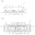
- FIG. 4 is a plan view illustrating a light emitting diode package according to an exemplary embodiment of the invention.
- a first lead frame 21 and a second lead frame 22 may be separated from each other by a gap (g) disposed between the two lead frames.
- the gap (g) may have an inclined or an angular line shape.
- the gap (g) may be positioned between inner ends of the first lead frame 21 and the second lead frame 22 .
- One or more of the inner ends of the first lead frame 21 and second lead frame 22 may have a leading end 213 a or a leading end 223 a and a trailing end 213 b or a trailing end 223 b .
- the leading ends and the trailing ends may not be distinguished from each other since the gap (g) and the inner ends may be present on a continuously straight line.
- leading end 213 a or the leading end 223 a and the trailing end 213 b or the trailing end 223 b may be distinguished from each other with reference to an imaginary reference line L crossing the center of the light emitting diode package 1 in a lateral direction.
- leading end 213 a or leading end 223 a may protrude from the corresponding lead frame 21 or lead frame 22 towards the other lead frame 22 or lead frame 21 beyond the trailing end 213 b or trailing end 223 b .
- the leading end 213 a of the first lead frame 21 may adjacently face the trailing end 223 b of the second lead frame 22
- the trailing end 213 b of the first lead frame 21 may adjacently face the leading end 223 a of the second lead frame 22 .
- a first enlarged region 214 may be formed between the first hole cup 212 of the first lead frame 21 and the leading end 213 a of the first lead frame 21 .
- a second enlarged region 224 may be formed between the second hole cup 222 of the second lead frame 22 and the leading end 223 a of the second lead frame 22 .
- One end of a bonding wire W 2 extending from the second light emitting diode chip 62 on the second lead frame 22 may be bonded to the first enlarged region 214
- one end of a bonding wire W 1 extending from the first light emitting diode chip 61 on the first lead frame 21 may be bonded to the second enlarged region 224 .
- a Zener diode 70 may be mounted on the second enlarged region 224 .
- the first enlarged region 214 and second enlarged region 224 may be of a reference size.
- the light emitting diode package may allow an increase in wire bonding regions corresponding to lead frames or a Zener diode mounting region.
- the wire bonding regions may be increased to that of at least a reference size or a sufficient size.
- the light emitting diode package may allow the increase in wire bonding regions without increasing the distance between light emitting diode chips mounted on adjacent lead frames.
- the light emitting diode package may allow an increase in wire bonding regions for lead frames or a Zener diode mounting region without decreasing the size of hole cups in application of the hole cups to adjacent lead frames.
Landscapes
- Engineering & Computer Science (AREA)
- Microelectronics & Electronic Packaging (AREA)
- Power Engineering (AREA)
- Computer Hardware Design (AREA)
- Manufacturing & Machinery (AREA)
- Physics & Mathematics (AREA)
- Condensed Matter Physics & Semiconductors (AREA)
- General Physics & Mathematics (AREA)
- Led Device Packages (AREA)
Applications Claiming Priority (2)
| Application Number | Priority Date | Filing Date | Title |
|---|---|---|---|
| KR1020110018519A KR101812761B1 (ko) | 2011-03-02 | 2011-03-02 | 발광다이오드 패키지 |
| KR10-2011-0018519 | 2011-03-02 |
Publications (2)
| Publication Number | Publication Date |
|---|---|
| US20120223343A1 US20120223343A1 (en) | 2012-09-06 |
| US8994061B2 true US8994061B2 (en) | 2015-03-31 |
Family
ID=46730740
Family Applications (1)
| Application Number | Title | Priority Date | Filing Date |
|---|---|---|---|
| US13/410,399 Active 2032-07-20 US8994061B2 (en) | 2011-03-02 | 2012-03-02 | Light emitting diode package |
Country Status (4)
| Country | Link |
|---|---|
| US (1) | US8994061B2 (ko) |
| KR (1) | KR101812761B1 (ko) |
| CN (1) | CN102655142B (ko) |
| TW (1) | TWI517458B (ko) |
Families Citing this family (16)
| Publication number | Priority date | Publication date | Assignee | Title |
|---|---|---|---|---|
| CN102403306B (zh) * | 2010-09-10 | 2015-09-02 | 展晶科技(深圳)有限公司 | 发光二极管封装结构 |
| KR101957884B1 (ko) * | 2012-05-14 | 2019-03-13 | 엘지이노텍 주식회사 | 발광 소자, 발광 소자 제조방법 및 조명 장치 |
| KR101886157B1 (ko) * | 2012-08-23 | 2018-08-08 | 엘지이노텍 주식회사 | 발광 소자 및 조명시스템 |
| KR101896691B1 (ko) * | 2012-10-11 | 2018-09-07 | 엘지이노텍 주식회사 | 발광 소자 및 조명 시스템 |
| JP6102187B2 (ja) * | 2012-10-31 | 2017-03-29 | 日亜化学工業株式会社 | 発光装置用パッケージ及びそれを用いた発光装置 |
| JP6107136B2 (ja) * | 2012-12-29 | 2017-04-05 | 日亜化学工業株式会社 | 発光装置用パッケージ及びそれを備える発光装置、並びにその発光装置を備える照明装置 |
| JP6081229B2 (ja) * | 2013-03-01 | 2017-02-15 | 株式会社東芝 | 半導体装置、無線装置、及び記憶装置 |
| TWI506822B (zh) * | 2013-03-25 | 2015-11-01 | I Chiun Precision Ind Co Ltd | 具有不對稱環壁的發光二極體晶片承載座 |
| KR101976547B1 (ko) * | 2013-04-29 | 2019-05-09 | 엘지이노텍 주식회사 | 발광 소자 및 이를 구비한 조명 시스템 |
| JP6261720B2 (ja) * | 2013-05-17 | 2018-01-17 | オスラム オプト セミコンダクターズ ゲゼルシャフト ミット ベシュレンクテル ハフツングOsram Opto Semiconductors GmbH | オプトエレクトロニクス素子およびオプトエレクトロニクス素子の製造方法 |
| CN104425694A (zh) * | 2013-08-29 | 2015-03-18 | 展晶科技(深圳)有限公司 | 发光二极管封装结构及其制造方法 |
| JP6413412B2 (ja) * | 2014-07-11 | 2018-10-31 | 日亜化学工業株式会社 | 半導体発光装置及びその製造方法 |
| CN106876555A (zh) * | 2017-04-17 | 2017-06-20 | 惠州雷曼光电科技有限公司 | 贴片式led支架以及贴片式led器件 |
| JP6652117B2 (ja) * | 2017-11-29 | 2020-02-19 | 日亜化学工業株式会社 | 樹脂パッケージおよび発光装置 |
| KR20190127218A (ko) * | 2018-05-04 | 2019-11-13 | 엘지이노텍 주식회사 | 반도체 소자 패키지 및 이를 포함하는 광조사장치 |
| KR20200007644A (ko) | 2018-07-13 | 2020-01-22 | 롬엔드하스전자재료코리아유한회사 | 복수 종의 호스트 재료 및 이를 포함하는 유기 전계 발광 소자 |
Citations (3)
| Publication number | Priority date | Publication date | Assignee | Title |
|---|---|---|---|---|
| US6054716A (en) * | 1997-01-10 | 2000-04-25 | Rohm Co., Ltd. | Semiconductor light emitting device having a protecting device |
| US20080316741A1 (en) * | 2007-06-21 | 2008-12-25 | Lee Kwang Cheol | Light emitting apparatus and surface light source apparatus having the same |
| US8188498B2 (en) * | 2008-11-25 | 2012-05-29 | Lg Innotek Co., Ltd. | Light emitting device package |
Family Cites Families (2)
| Publication number | Priority date | Publication date | Assignee | Title |
|---|---|---|---|---|
| JP5052326B2 (ja) * | 2007-10-31 | 2012-10-17 | シャープ株式会社 | チップ部品型led及びその製造方法 |
| US7923739B2 (en) * | 2009-06-05 | 2011-04-12 | Cree, Inc. | Solid state lighting device |
-
2011
- 2011-03-02 KR KR1020110018519A patent/KR101812761B1/ko active IP Right Grant
-
2012
- 2012-03-01 TW TW101106630A patent/TWI517458B/zh active
- 2012-03-02 CN CN201210052644.6A patent/CN102655142B/zh active Active
- 2012-03-02 US US13/410,399 patent/US8994061B2/en active Active
Patent Citations (3)
| Publication number | Priority date | Publication date | Assignee | Title |
|---|---|---|---|---|
| US6054716A (en) * | 1997-01-10 | 2000-04-25 | Rohm Co., Ltd. | Semiconductor light emitting device having a protecting device |
| US20080316741A1 (en) * | 2007-06-21 | 2008-12-25 | Lee Kwang Cheol | Light emitting apparatus and surface light source apparatus having the same |
| US8188498B2 (en) * | 2008-11-25 | 2012-05-29 | Lg Innotek Co., Ltd. | Light emitting device package |
Also Published As
| Publication number | Publication date |
|---|---|
| US20120223343A1 (en) | 2012-09-06 |
| CN102655142B (zh) | 2017-06-23 |
| KR20120099963A (ko) | 2012-09-12 |
| TW201238104A (en) | 2012-09-16 |
| CN102655142A (zh) | 2012-09-05 |
| KR101812761B1 (ko) | 2017-12-28 |
| TWI517458B (zh) | 2016-01-11 |
Similar Documents
| Publication | Publication Date | Title |
|---|---|---|
| US8994061B2 (en) | Light emitting diode package | |
| US9929330B2 (en) | Light emitting diode package | |
| US8283693B2 (en) | Light emitting device with a lens of silicone | |
| US20130292812A1 (en) | Lead frame for semiconductor device and semiconductor device package using the lead frame | |
| US9515241B2 (en) | LED structure, metallic frame of LED structure, and carrier module | |
| TWI506821B (zh) | 發光二極體封裝結構及其製造方法 | |
| US20170358561A1 (en) | Led leadframe and led packaging structure | |
| TW201436301A (zh) | 發光二極體封裝結構及其製造方法 | |
| US20140217602A1 (en) | Semiconductor device | |
| US9748459B2 (en) | Method for manufacturing improved chip-on-board type light emitting device package and such manufactured chip-on-board type light emitting device package | |
| TWI509834B (zh) | 發光二極體封裝結構及其製造方法 | |
| WO2006071098A1 (en) | Lead frame, semiconductor package employing the lead frame and method for manufacturing the semiconductor package | |
| KR101078028B1 (ko) | 발광 소자 패키지 및 발광 소자 패키지용 리드 프레임 | |
| TW201409763A (zh) | 發光二極體封裝結構及其製造方法 | |
| KR100733074B1 (ko) | 리드프레임 구조체 및 이를 채용한 반도체 패키지 및 그제조방법 | |
| TW201448286A (zh) | 發光二極體封裝結構及其製造方法 | |
| TWI531096B (zh) | 側面發光型發光二極體封裝結構及其製造方法 | |
| KR101186649B1 (ko) | 사이드뷰 발광다이오드 패키지 | |
| TWI492424B (zh) | 發光二極體封裝結構 | |
| KR20110080902A (ko) | Led 패키지 | |
| KR102374676B1 (ko) | 발광 다이오드 패키지 및 그 제조 방법 | |
| KR20130023046A (ko) | 엘이디 패키지용 리드 프레임 | |
| KR20120134785A (ko) | 발광다이오드 패키지 | |
| KR20100020770A (ko) | 반도체 패키지 |
Legal Events
| Date | Code | Title | Description |
|---|---|---|---|
| AS | Assignment |
Owner name: SEOUL SEMICONDUCTOR CO., LTD., KOREA, REPUBLIC OF Free format text: ASSIGNMENT OF ASSIGNORS INTEREST;ASSIGNORS:KANG, DO HYOUNG;KIM, OH SUG;REEL/FRAME:027795/0877 Effective date: 20120302 |
|
| FEPP | Fee payment procedure |
Free format text: PAYOR NUMBER ASSIGNED (ORIGINAL EVENT CODE: ASPN); ENTITY STATUS OF PATENT OWNER: LARGE ENTITY |
|
| STCF | Information on status: patent grant |
Free format text: PATENTED CASE |
|
| MAFP | Maintenance fee payment |
Free format text: PAYMENT OF MAINTENANCE FEE, 4TH YEAR, LARGE ENTITY (ORIGINAL EVENT CODE: M1551) Year of fee payment: 4 |
|
| MAFP | Maintenance fee payment |
Free format text: PAYMENT OF MAINTENANCE FEE, 8TH YEAR, LARGE ENTITY (ORIGINAL EVENT CODE: M1552); ENTITY STATUS OF PATENT OWNER: LARGE ENTITY Year of fee payment: 8 |