US8833298B2 - Film forming apparatus - Google Patents
Film forming apparatus Download PDFInfo
- Publication number
- US8833298B2 US8833298B2 US13/537,597 US201213537597A US8833298B2 US 8833298 B2 US8833298 B2 US 8833298B2 US 201213537597 A US201213537597 A US 201213537597A US 8833298 B2 US8833298 B2 US 8833298B2
- Authority
- US
- United States
- Prior art keywords
- reaction chamber
- protection pipe
- film forming
- forming apparatus
- substrates
- Prior art date
- Legal status (The legal status is an assumption and is not a legal conclusion. Google has not performed a legal analysis and makes no representation as to the accuracy of the status listed.)
- Active, expires
Links
- 238000006243 chemical reaction Methods 0.000 claims abstract description 143
- 239000010408 film Substances 0.000 claims abstract description 58
- 239000002994 raw material Substances 0.000 claims abstract description 38
- 239000000758 substrate Substances 0.000 claims abstract description 29
- 239000010409 thin film Substances 0.000 claims abstract description 19
- 238000010438 heat treatment Methods 0.000 claims abstract description 10
- 235000012431 wafers Nutrition 0.000 description 90
- 239000007789 gas Substances 0.000 description 33
- 238000005452 bending Methods 0.000 description 15
- 230000015572 biosynthetic process Effects 0.000 description 9
- VYPSYNLAJGMNEJ-UHFFFAOYSA-N Silicium dioxide Chemical compound O=[Si]=O VYPSYNLAJGMNEJ-UHFFFAOYSA-N 0.000 description 6
- 238000000034 method Methods 0.000 description 6
- 230000008901 benefit Effects 0.000 description 4
- PZPGRFITIJYNEJ-UHFFFAOYSA-N disilane Chemical compound [SiH3][SiH3] PZPGRFITIJYNEJ-UHFFFAOYSA-N 0.000 description 4
- NJPPVKZQTLUDBO-UHFFFAOYSA-N novaluron Chemical compound C1=C(Cl)C(OC(F)(F)C(OC(F)(F)F)F)=CC=C1NC(=O)NC(=O)C1=C(F)C=CC=C1F NJPPVKZQTLUDBO-UHFFFAOYSA-N 0.000 description 4
- 229910021417 amorphous silicon Inorganic materials 0.000 description 3
- 238000000354 decomposition reaction Methods 0.000 description 3
- 230000003247 decreasing effect Effects 0.000 description 3
- 230000000694 effects Effects 0.000 description 3
- 238000012423 maintenance Methods 0.000 description 3
- 238000005259 measurement Methods 0.000 description 3
- 238000005192 partition Methods 0.000 description 3
- 238000004088 simulation Methods 0.000 description 3
- 239000011261 inert gas Substances 0.000 description 2
- 239000002184 metal Substances 0.000 description 2
- 239000004065 semiconductor Substances 0.000 description 2
- 238000012546 transfer Methods 0.000 description 2
- 229910007264 Si2H6 Inorganic materials 0.000 description 1
- 229910052581 Si3N4 Inorganic materials 0.000 description 1
- 238000009529 body temperature measurement Methods 0.000 description 1
- 238000004364 calculation method Methods 0.000 description 1
- 238000004140 cleaning Methods 0.000 description 1
- 239000000470 constituent Substances 0.000 description 1
- 238000009826 distribution Methods 0.000 description 1
- 238000002474 experimental method Methods 0.000 description 1
- 238000004519 manufacturing process Methods 0.000 description 1
- 239000002245 particle Substances 0.000 description 1
- 238000010926 purge Methods 0.000 description 1
- 230000003252 repetitive effect Effects 0.000 description 1
- HQVNEWCFYHHQES-UHFFFAOYSA-N silicon nitride Chemical compound N12[Si]34N5[Si]62N3[Si]51N64 HQVNEWCFYHHQES-UHFFFAOYSA-N 0.000 description 1
- 229910052814 silicon oxide Inorganic materials 0.000 description 1
Images


Classifications
-
- C—CHEMISTRY; METALLURGY
- C23—COATING METALLIC MATERIAL; COATING MATERIAL WITH METALLIC MATERIAL; CHEMICAL SURFACE TREATMENT; DIFFUSION TREATMENT OF METALLIC MATERIAL; COATING BY VACUUM EVAPORATION, BY SPUTTERING, BY ION IMPLANTATION OR BY CHEMICAL VAPOUR DEPOSITION, IN GENERAL; INHIBITING CORROSION OF METALLIC MATERIAL OR INCRUSTATION IN GENERAL
- C23C—COATING METALLIC MATERIAL; COATING MATERIAL WITH METALLIC MATERIAL; SURFACE TREATMENT OF METALLIC MATERIAL BY DIFFUSION INTO THE SURFACE, BY CHEMICAL CONVERSION OR SUBSTITUTION; COATING BY VACUUM EVAPORATION, BY SPUTTERING, BY ION IMPLANTATION OR BY CHEMICAL VAPOUR DEPOSITION, IN GENERAL
- C23C16/00—Chemical coating by decomposition of gaseous compounds, without leaving reaction products of surface material in the coating, i.e. chemical vapour deposition [CVD] processes
- C23C16/44—Chemical coating by decomposition of gaseous compounds, without leaving reaction products of surface material in the coating, i.e. chemical vapour deposition [CVD] processes characterised by the method of coating
-
- H—ELECTRICITY
- H01—ELECTRIC ELEMENTS
- H01L—SEMICONDUCTOR DEVICES NOT COVERED BY CLASS H10
- H01L21/00—Processes or apparatus adapted for the manufacture or treatment of semiconductor or solid state devices or of parts thereof
- H01L21/67—Apparatus specially adapted for handling semiconductor or electric solid state devices during manufacture or treatment thereof; Apparatus specially adapted for handling wafers during manufacture or treatment of semiconductor or electric solid state devices or components ; Apparatus not specifically provided for elsewhere
- H01L21/67005—Apparatus not specifically provided for elsewhere
- H01L21/67242—Apparatus for monitoring, sorting or marking
- H01L21/67248—Temperature monitoring
-
- B—PERFORMING OPERATIONS; TRANSPORTING
- B05—SPRAYING OR ATOMISING IN GENERAL; APPLYING FLUENT MATERIALS TO SURFACES, IN GENERAL
- B05C—APPARATUS FOR APPLYING FLUENT MATERIALS TO SURFACES, IN GENERAL
- B05C11/00—Component parts, details or accessories not specifically provided for in groups B05C1/00 - B05C9/00
-
- C—CHEMISTRY; METALLURGY
- C23—COATING METALLIC MATERIAL; COATING MATERIAL WITH METALLIC MATERIAL; CHEMICAL SURFACE TREATMENT; DIFFUSION TREATMENT OF METALLIC MATERIAL; COATING BY VACUUM EVAPORATION, BY SPUTTERING, BY ION IMPLANTATION OR BY CHEMICAL VAPOUR DEPOSITION, IN GENERAL; INHIBITING CORROSION OF METALLIC MATERIAL OR INCRUSTATION IN GENERAL
- C23C—COATING METALLIC MATERIAL; COATING MATERIAL WITH METALLIC MATERIAL; SURFACE TREATMENT OF METALLIC MATERIAL BY DIFFUSION INTO THE SURFACE, BY CHEMICAL CONVERSION OR SUBSTITUTION; COATING BY VACUUM EVAPORATION, BY SPUTTERING, BY ION IMPLANTATION OR BY CHEMICAL VAPOUR DEPOSITION, IN GENERAL
- C23C16/00—Chemical coating by decomposition of gaseous compounds, without leaving reaction products of surface material in the coating, i.e. chemical vapour deposition [CVD] processes
Definitions
- the present invention relates to a film forming apparatus for forming a thin film on a substrate.
- a manufacturing process of a semiconductor integrated circuit includes various film forming processes for forming several thin films on a substrate, such as a semiconductor wafer (hereinafter, referred to as a wafer).
- a so-called batch-type film forming apparatus may be used during a film forming process.
- Such a film forming apparatus includes a wafer boat holding a plurality of wafers at intervals, a reaction chamber accommodating the wafer boat, a support unit supporting the reaction chamber, a raw material gas supply pipe extended along the wafer boat inside the reaction chamber and for supplying a raw material gas for forming a thin film on the wafers to the wafers, and a heater disposed outside the reaction chamber and for heating the wafers held by the wafer boat.
- a temperature measuring unit is provided along the wafer boat so as to measure a temperature of the wafers.
- the temperature measuring unit may be inserted into a protection pipe extended along the wafer boat (for example, Patent Reference 1).
- the wafer boat is accommodated in the reaction chamber, the wafers held by the wafer boat are heated by using the heater so that a temperature of the wafers reaches a predetermined film forming temperature, and then the raw material gas is supplied. Accordingly, the raw material gas is decomposed by heat of the wafers, and a thin film is formed on the wafers by a decomposition product.
- the decomposition product is not only deposited on the wafers, but also on the wafer boat, the reaction chamber, and the protection pipe.
- the outer surface of the protection pipe may be adhered to the inner surface of the reaction chamber due to the decomposition product.
- a stress may be applied to the protection pipe while decreasing the temperature of the wafers after film formation, thereby damaging the protection pipe.
- Patent Reference 1 Japanese Laid-Open Patent Publication No. 2002-270593
- the present invention provides a film forming apparatus capable of preventing an outer surface of a protection pipe from being adhered to an inner surface of a reaction chamber.
- a film forming apparatus including: a substrate holding unit which holds a plurality of substrates such that the plurality of substrates are stacked on each other at intervals; a reaction chamber which accommodates the substrate holding unit; a raw material gas supply pipe which supplies a raw material gas of a thin film formed on the plurality of substrates to the plurality of substrate held by the substrate holding unit accommodated in the reaction chamber; a support unit which supports the reaction chamber; a heating unit which is disposed outside the reaction chamber and heats the plurality of substrates; a protection pipe which includes one end portion fixed to the support unit, is extended along an arrangement direction of the plurality of substrates between the substrate holding unit and the reaction chamber, and includes a temperature measuring unit inserted therein; and a protrusion portion which is provided on at least one of an outer surface of the protection pipe and an inner surface of the reaction chamber, and provides a gap between the outer surface of the protection pipe and the inner surface of the reaction chamber.
- FIG. 1 is a schematic cross-sectional view showing a film forming apparatus according to an embodiment of the present invention
- FIG. 2 is a schematic top view showing a location relationship between a protection pipe and a reaction chamber of the film forming apparatus of FIG. 1 ;
- FIGS. 3A and 3B are views for explaining a reason for a stress applied to the protection pipe in the film forming apparatus of FIG. 1 ;
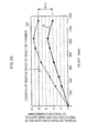
- FIG. 4 is a graph showing a result of measuring a stress applied to the protection pipe in the film forming apparatus of FIG. 1 ;
- FIGS. 5A and 5B are respectively a view and a graph for explaining an effect by a protrusion portion provided at a leading end portion of the protection pipe of the film forming apparatus of FIG. 1 ;
- FIGS. 6A and 6B are schematic top views showing location relationships between the protection pipe and the reaction chamber in modified examples of the film forming apparatus of FIG. 1 .
- FIG. 1 is a schematic cross-sectional view showing a film forming apparatus 10 according to an embodiment of the present invention.
- the film forming apparatus 10 includes a wafer boat 21 which holds a plurality of wafers W such that the plurality of wafers W are stacked on each other at intervals in an up-and-down direction, a reaction chamber 22 which accommodates the wafer boat 21 , an outer chamber 23 which accommodates the reaction chamber 22 , and a manifold 24 which supports the reaction chamber 22 and the outer chamber 23 .
- a raw material gas nozzle 25 which supplies a raw material gas to the wafers W held by the wafer boat 21 and a protection pipe 26 into which a temperature measuring unit, for example, a thermocouple or a thermoresistor, is inserted to protect the temperature measuring unit from the raw material gas or the like, are provided at the film forming apparatus 10 .
- the raw material gas nozzle 25 and the protection pipe 26 are extended along the wafer boat 21 in a space between the wafer boat 21 and the reaction chamber 22 , and are disposed across the wafer boat 21 from each other.
- a heater 27 which is disposed to surround an outer circumference of the outer chamber 23 and heats the wafers W held by the wafer boat 21 is provided at the film forming apparatus 10 .
- the heater 27 may include a plurality of partition heaters disposed in an up-and-down direction, and a power supply device (not shown) is connected to each partition heater.
- an additional heater which heats the wafers W from a top of the outer chamber 23 may be provided at the top of the outer chamber 23 .
- the wafer boat 21 is formed of, for example, quartz glass, and includes a top lid portion 21 a , a bottom lid portion 21 b , and, for example, three supports 21 c (only two are shown in FIG. 1 ) which support the top lid portion 21 a to the bottom lid portion 21 b .
- a plurality of slits are provided on the supports 21 c .
- Each of the plurality of slits is provided so as to be located at the same height as a corresponding slit of each support 21 c , and thus the wafers W are supported by such slits.
- a number and interval of the slits may be determined according to a size of the wafers W, a number of the wafers W to be processed via one film forming process, or a size of the reaction chamber 22 .
- a bottom of the wafer boat 21 is supported by a pedestal 28 , and the pedestal 28 is fixed on an elevation plate 29 .
- the elevation plate 29 may be moved up and down by an elevation mechanism (not shown).
- the elevation plate 29 is moved up by the elevation mechanism, and contacts a bottom surface of the manifold 24 via a seal member, for example, an O-ring or a metal seal.
- a space hereinafter, referred to as an inner space
- the elevation plate 29 and furthermore the wafer boat 21 , are moved down by the elevation mechanism.
- the reaction chamber 22 is formed of, for example, quartz glass having a cylindrical shape including a lid, and a bottom portion of the reaction chamber 22 is supported by a flange portion provided at an inner circumference of the manifold 24 .
- the outer chamber 23 surrounding an outer side of the reaction chamber 22 is formed of, for example, quartz glass having a cylindrical shape including a lid. Also, the outer chamber 23 is hermetically adhered to a top surface of the manifold 24 via a seal member, for example, an O-ring or a metal seal.
- one or at least two openings are provided at the reaction chamber 22 , and thus an inner space of the reaction chamber 22 and an outer space of the reaction chamber 22 (an inner space of the outer chamber 23 ) communicate with each other through the opening.
- an exhaust pipe (not shown) is connected to the manifold 24 , and the exhaust pipe is connected to an exhaust apparatus including a vacuum pump. Accordingly, the raw material gas supplied from the raw material gas nozzle 25 to the wafers W described below is exhausted through the openings of the reaction chamber 22 and the exhaust pipe of the outer chamber 23 .
- a pressure controller (not shown) is provided at the exhaust pipe, and thus a pressure inside the reaction chamber 22 is adjusted.
- An upper flange of the manifold 24 is attached to a base unit 30 by a plurality of bolts and nuts (not shown). Accordingly, the manifold 24 supports the reaction chamber 22 and the outer chamber 23 to the base unit 30 .
- the raw material gas nozzle 25 is formed of, for example, quartz glass, reaches the inner space through a nozzle introduction portion 24 a provided at the manifold 24 , and is extended along the wafer boat 21 by bending upward.
- a seal member 24 b for example, an O-ring, and a connector 24 c which maintains airtightness by pushing the seal member toward the raw material gas nozzle 25 , are provided at an end portion of the nozzle introduction portion 24 a .
- an end portion of the raw material gas nozzle 25 outside the manifold 24 is connected to a raw material supply system (not shown), and the raw material gas is supplied to the raw material gas nozzle 25 from the raw material supply system.
- a plurality of openings 25 a which are opened toward the wafers W held by the wafer boat 21 are provided at the raw material gas nozzle 25 , and the raw material gas supplied from the raw material supply system is supplied to the wafers W through the openings 25 a.
- the raw material supply system includes a gas cylinder (not shown) in which the raw material gas corresponding to a thin film to be formed on the wafers W is stored, and a pressure controller (for example, a regulator) or a flow rate adjustor (for example, a mass flow controller) (both not shown) is provided at a pipe connecting the gas cylinder and the raw material gas nozzle 25 , and thus the raw material gas is supplied to the raw material gas nozzle 25 while its flow rate is being controlled.
- a pressure controller for example, a regulator
- a flow rate adjustor for example, a mass flow controller
- the protection pipe 26 is formed of, for example, quartz glass, reaches the inner space through a protection pipe introduction portion 24 d provided at the manifold 24 , and is extended along the wafer boat 21 by bending upward.
- the seal member 24 b and the connector 24 c are also provided at the protection pipe introduction portion 24 d , and thus airtightness is maintained.
- a plurality of thermocouples 26 b (only one is shown in FIG. 1 ), for example, are inserted into the protection pipe 26 . Temperature measuring ends of each thermocouple 26 b are disposed at different locations in a height direction, and thus a temperature distribution of the wafer boat 21 in a length direction may be obtained.
- a temperature adjustor (not shown) is connected to the thermocouples 26 b .
- Each power supply device of the partition heaters described above is controlled based on temperature measurement results of the thermocouples 26 b , and thus the plurality of wafers W held by the wafer boat 21 may be uniformly heated.
- FIG. 2 is a schematic partial top view of the film forming apparatus 10 , wherein a location relationship between the wafer boat 21 , the reaction chamber 22 , and the protection pipe 26 is shown.
- a groove portion 22 a sunken to the wafer boat 21 is provided on the reaction chamber 22 .
- the groove portion 22 a is extended from a bottom to a top of the reaction chamber 22 . Since an inner surface of the reaction chamber 22 is outwardly sunken by the groove portion 22 a , a space for disposing the protection pipe 26 may be increased. In other words, the providing of the groove portion 22 a on the reaction chamber 22 is effective when the space between the reaction chamber 22 and the wafer boat 21 is narrow.
- the raw material gas supplied from the raw material gas nozzle 25 may easily flow into a space between the wafers W, and thus film forming efficiency is improved.
- protrusion portions 26 a are provided near a top of the protection pipe 26 (refer to FIG. 1 ).
- the protrusion portions 26 a are disposed at an interval of about 120° around the protection pipe 26 .
- a shape of the protrusion portions 26 a is not limited to a hemispherical shape shown in FIG. 2 , and may be a column shape (a cylindrical shape or a horn shape) or a pin shape. Also, to minimize a contact area between the protrusion portions 26 a and the inner surface of the reaction chamber 22 , if the protrusion portions 26 a have a column shape, leading end portions may be round.
- a size of the protrusion portions 26 a may be determined based on a depth or width of the groove portion 22 a , an outer diameter of the protection pipe 26 , an interval between the reaction chamber 22 and the wafer boat 21 , or the like.
- a height of the protrusion portions 26 a (a protruded amount from an outer surface of the protection pipe 26 ) is about 4 mm.
- the leading end portions of the two protrusion portions 26 a contact an inner surface of the groove portion 22 a , and the interval angle of the two protrusion portions 26 a is about 120°, a location misalignment of the protection pipe 26 in a direction along the inner surface of the reaction chamber 22 may be effectively prevented.
- the wafers W are loaded from a wafer carrier to the wafer boat 21 unloaded from the reaction chamber 22 by using a wafer transfer mechanism (not shown) provided together with the film forming apparatus 10 .
- the wafer boat 21 is loaded into the reaction chamber 22 , and the inner space (the space defined by the outer chamber 23 , the manifold 24 , and the elevation plate 29 ) is evacuated to a predetermined pressure while the inner space is purged as, for example, an inert gas is supplied from a purge gas supply nozzle (not shown).
- the wafers W are then heated up to a predetermined film forming temperature (for example, 500° C.
- disilane Si 2 H 6
- disilane Si 2 H 6
- disilane is supplied from the raw material gas nozzle 25
- disilane is thermally decomposed by heat of the wafers W
- amorphous silicon thin film is formed on the wafers W.
- the supplying of disilane is stopped, the heating of the wafers W is stopped, the inner space is purged by the inert gas, and then the wafer boat 21 is unloaded from the reaction chamber 22 .
- the wafers W are carried from the wafer boat 21 to, for example, the wafer carrier by using the transfer mechanism, thereby ending a film forming process.
- FIG. 3A is a view showing the manifold 24 , the protection pipe introduction portion 24 d , and the protection pipe 26 when the outer chamber 23 , the reaction chamber 22 , and the wafer boat 21 are at room temperature after installing or maintaining the film forming apparatus 10 .
- the protection pipe introduction portion 24 d is extended from the manifold 24 almost horizontally, and thus the protection pipe 26 is horizontally inserted into the manifold 24 . Also, the protection pipe 26 is bent upward in the inner space.
- FIG. 3B is a view showing the manifold 24 , the protection pipe introduction portion 24 d , and the protection pipe 26 when the outer chamber 23 , the reaction chamber 22 , and the wafer boat 21 are heated during, for example, the film formation.
- the protection pipe introduction portion 24 d is tilted downward by an angle ⁇ as the manifold 24 is deformed due to heat.
- a temperature of the manifold 24 is about 195° C.
- a tilt angle ⁇ of the protection pipe introduction portion 24 d is about 0.35° when the wafers W are heated up to 400° C.
- the protection pipe introduction portion 24 d is tilted
- the protection pipe 26 is also tilted, and thus the protection pipe 26 is tilted toward the inner surface of the reaction chamber 22 in the space between the wafer boat 21 and the reaction chamber 22 .
- the protection pipe 26 tilted toward the reaction chamber 22 bends along the inner surface of the groove portion 22 a (hereinafter, for convenience, referred to as the inner surface of the reaction chamber 22 ), and thus the outer surface of the protection pipe 26 contacts the inner surface of the reaction chamber 22 in a wide range.
- the outer surface of the protection pipe 26 may be relatively strongly adhered to the inner surface of the reaction chamber 22 due to a film deposited on the reaction chamber 22 or protection pipe 26 , during the film formation.
- the protection pipe introduction portion 24 d is returned to a horizontal direction ( FIG. 3A ). Then, a bending stress is applied to the protection pipe 26 having the outer surface adhered to the inner surface of the reaction chamber 22 .
- the protection pipe introduction portion 24 d is tilted by tilting the manifold 24 , thereby measuring a weight applied to the protection pipe 26 by using a push-pull gauge.
- the bending stress applied to the protection pipe 26 is obtained from the obtained weight, a bending amount of the protection pipe 26 , and a shape of the protection pipe 26 .
- bending stresses were obtained when a length of an upright portion (a portion in the space between the wafer boat 21 and the reaction chamber 22 ) of the protection pipe 26 was about 1350 mm, at locations where heights from a horizontal portion (a portion supported by the protection pipe introduction portion 24 d ) of the protection pipe 26 were 150 mm, 300 mm, 450 mm, and 1330 mm.
- FIG. 4 The result of measuring the bending stresses is shown in FIG. 4 .
- a bending stress applied to the protection pipe 26 is increased in a straight line as the tilt angle ⁇ of the protection pipe introduction portion 24 d is increased.
- a size of the bending stress is larger closer to a bottom of the upright portion of the protection pipe 26 .
- the bending stress applied to the protection pipe 26 at the location 150 mm from the bottom of the upright portion of the protection pipe 26 is about 6 times larger than the bending stress applied to the protection pipe 26 at the location 1330 mm from the bottom.
- the protection pipe 26 may be damaged at a portion below the adhered portion.
- the protrusion portions 26 a are provided at a top (leading end) portion of the protection pipe 26 , even if the protection pipe 26 tilts towards the inner surface of the reaction chamber 22 due to thermal deformation of the manifold 24 during a temperature increase, only the protrusion portions 26 a contact the inner surface of the reaction chamber 22 , and thus the outer surface of the protection pipe 26 does not contact the inner surface of the reaction chamber 22 . Accordingly, even if a film is formed on the outer surface of the protection pipe 26 or the inner surface of the reaction chamber 22 , the outer surface of the protection pipe 26 may be prevented from being adhered to the inner surface of the reaction chamber 22 .
- the leading end portion of the protection pipe 26 is fixed to the inner surface of the reaction chamber 22 via the protrusion portions 26 a , but since a stress applied to the leading end portion of the protection pipe 26 is relatively small as shown in FIG. 4 , the protection pipe 26 may not be damaged. Also, even if the protrusion portions 26 a are adhered to the inner surface of the reaction chamber 22 , a contact area is smaller than when the outer surface of the protection pipe 26 is adhered to the inner surface of the reaction chamber 22 , and thus the protrusion portions 26 a are easily detached from the inner surface of the reaction chamber 22 during a temperature decrease. Accordingly, the leading end portion of the protection pipe 26 is to be a free end, and thus a bending stress is not applied to the protection pipe 26 .
- FIG. 5A shows a model used in the simulation.
- the length of the upright portion of the protection pipe 26 was 1350 mm, and a thickness of the protection pipe 26 was about 12 mm.
- an interval between the protection pipe 26 and the reaction chamber 22 was about 8 mm at a bottom end portion of the protection pipe 26 , and about 4 mm at the leading end portion of the protection pipe 26 .
- the upright portion of the protection pipe 26 was slightly tilted towards the inner surface of the reaction chamber 22 .
- a location of the protrusion portions 26 a was at about 20 mm from the leading end of the protection pipe 26 .
- a height of the protrusion portions 26 a (a protruded amount from the outer surface of the protection pipe 26 ) was about 4 mm.
- the protrusion portions 26 a contacted the inner surface of the reaction chamber 22 (that is, the leading end portion of the protection pipe 26 was about 4 mm away from the inner surface of the reaction chamber 22 due to the protrusion portions 26 a ).
- the tilt angle ⁇ of the protection pipe introduction portion 24 d of the manifold 24 was about 1.0°.
- a degree of tilt angle of the protection pipe 26 is schematically shown in FIG. 5A with a dotted line as if the reaction chamber 22 did not exist at this tilt angle ⁇ .
- FIG. 5B shows a result of calculating how the protection pipe 26 is bent.
- a location of the leading end portion of the protection pipe 26 was fixed by the protrusion portions 26 a , and the protection pipe 26 was bent between the leading end portion and the bottom end portion toward the inner surface of the reaction chamber 22 .
- the protrusion portions 26 a having a height of about 4 mm at the leading end portion of the protection pipe 26 , the outer surface of the protection pipe 26 may be prevented from contacting the inner surface of the reaction chamber 22 .
- the outer surface of the protection pipe 26 may be adhered to the inner surface of the reaction chamber 22 in a wide range during the film formation. Moreover, if the outer surface of the protection pipe 26 is adhered to the inner surface of the reaction chamber 22 in the range from the height of about 750 mm to the top, the outer surface of the protection pipe 26 is relatively strongly adhered to the inner surface of the reaction chamber 22 while a relatively large bending stress is applied to the bottom of the protection pipe 26 (refer to FIG. 4 ), and thus it is highly likely that the protection pipe 26 is damaged.
- the groove portion 22 a is provided to be protruded outwardly along the protection pipe 26 on the reaction chamber 22 in the above embodiments, but the groove portion 22 a is not necessarily required.
- the protection pipe 26 including the protrusion portions 26 a may be disposed to the reaction chamber 22 not having a groove portion.
- only one protrusion portion 26 a may be provided at the protection pipe 26 .
- two protrusion portions 26 a are provided in order to prevent a location misalignment of the protection pipe 26 to a direction along the inner surface of the reaction chamber 22 .
- the angle interval between the two protrusion portions 26 a is not limited to about 120°, and may be suitably determined as long as the outer surface of the protection pipe 26 does not contact the inner surface of the reaction chamber 22 (groove portion 22 a ).
- the protrusion portions 26 a may be provided at the groove portion 22 a of the reaction chamber 22 as shown in FIG. 6B , or at the inner surface of the reaction chamber 22 not having the groove portion 22 a , instead of at the protection pipe 26 .
- one protrusion portion 26 a may be provided, or a plurality (preferably two) of protrusion portions 26 a may be provided.
- the protrusion portions 26 a may be provided at both the outer surface of the protection pipe 26 and the inner surface of the reaction chamber 22 .
- the protrusion portions 26 a provided at the leading end portion of the protection pipe 26 are disposed to contact the inner surface of the groove portion 22 a of the reaction chamber 22 , but the protection pipe 26 may be disposed such that the protrusion portions 26 a do not contact the inner surface of the groove portion 22 a at room temperature. In this case, the outer surface of the protection pipe 26 definitely does not contact the inner surface of the groove portion 22 a during a temperature increase.
- the protection pipe 26 may vibrate in some cases, and thus the protrusion portions 26 a may collide with the inner surface of the groove portion 22 a , thereby generating a particle.
- the protrusion portions 26 a may contact the inner surface of the groove portion 22 a.
- the protection pipe 26 may be far from the inner surface of the reaction chamber 22 .
- the protection pipe 26 tilts towards the inner surface of the reaction chamber 22 due to the thermal deformation of the manifold 24 , a distance between the thermocouple 26 b and the wafer boat 21 in the protection pipe 26 is changed.
- the distance is changed, the temperature of the wafers W held by the wafer boat 21 is changed, and thus reproducibility of a wafer temperature may be deteriorated.
- the protection pipe 26 when the protection pipe 26 is disposed such that the protrusion portions 26 a of the protection pipe 26 pre-contact the reaction chamber 22 (or the groove portion 22 a ), the change of the interval between the protection pipe 26 and the wafer boat 21 may be reduced. Accordingly, junction/disjunction of the protrusion portions 26 a to the reaction chamber 22 (or the groove portion 22 a ) may be determined according to circumstances.
- the location of the protrusion portions 26 a is not limited to the leading end portion of the protection pipe 26 , and may be a center portion (a center portion of the inner surface of the reaction chamber 22 ) because the outer surface of the protection pipe 26 can be prevented from directly contacting the inner surface of the reaction chamber 22 by using the protrusion portions 26 a provided at the center portion. Accordingly, the outer surface of the protection pipe 26 is prevented from being adhered to the inner surface of the reaction chamber 22 .
- the protrusion portions 26 a provided at the center portion is adhered to the inner surface of the reaction chamber 22 , the protrusion portions 26 a are easily detached from the inner surface of the reaction chamber 22 since a contact area between the protrusion portions 26 a and the inner surface of the reaction chamber 22 is small.
- the outer surface of the protection pipe 26 is not strongly adhered to the inner surface of the reaction chamber 22 via the protrusion portions 26 a even when the protrusion portions 26 a are provided at a location about 700 mm to about 800 mm from a bottom of the protection pipe 26 .
- the reaction chamber 22 is provided on an inner side of the outer chamber 23 , and the wafer boat 21 , the raw material gas nozzle 25 , and the protection pipe 26 are disposed on an inner side of the reaction chamber 22 .
- a thin film may not be formed on the inner surface of the outer chamber 23 .
- a thin film is formed on the inner surface of the reaction chamber 22 , but since the reaction chamber 22 is smaller than the outer chamber 23 , cleaning for removing the thin film formed on the inner surface may be easily performed.
- preparing and suitably exchanging a plurality of reaction chambers 22 costs less than preparing and suitably exchanging a plurality of outer chambers 23 .
- the protection pipe 26 may be disposed to extend along the inner surface of the outer chamber 23 .
- the outer chamber 23 may be used as a reaction chamber.
- a plurality of protection pipes 26 having different lengths (heights) may be provided, and one thermocouple may be inserted therein respectively.
- the protrusion portions 26 a may be provided for each protection pipe 26 .
- a thin film formed on the wafers W is not limited to an amorphous silicon film, and for example, may be a silicon oxide film, a silicon nitride film or the like.
- a depth (sunken amount) or a width of the groove portion 22 a provided on the reaction chamber 22 may be suitably determined according to the outer diameter of the protection pipe 26 used.
- a sunken shape is not limited to a circular cross-section (top shape), and may have a rectangular cross-section.
- three protrusion portions 26 a may be provided on the protection pipe 26 according to each surface of the groove portion 22 a having the rectangular cross-section.
- the length and diameter of the protection pipe 26 , the size of the protrusion portions 26 a , etc. described above are only examples, and may be suitably determined in each of film forming apparatuses according to a size of the wafers W on which a thin film is formed or a number of wafers W per one film forming process.
- a film forming apparatus capable of preventing an outer surface of a protection pipe from being adhered to an inner surface of a reaction chamber.
- the protection pipe since one end portion of the protection pipe is fixed to a support unit supporting the reaction chamber, when the support unit is thermally deformed by heat from a heating unit, the protection pipe may tilt towards the inner surface of the reaction chamber. However, even in this case, the outer surface of the protection pipe is prevented from contacting the inner surface of the reaction chamber by a protrusion portion.
- the outer surface of the protection pipe is prevented from being adhered to the inner surface of the reaction chamber.
- an operation of separating the protection pipe from the inner surface of the reaction chamber is not required during maintenance.
- a large stress is not applied to the protection pipe if the outer surface of the protection pipe is not adhered to the inner surface of the reaction chamber, and thus the protection pipe may not be damaged.
Landscapes
- Chemical & Material Sciences (AREA)
- Engineering & Computer Science (AREA)
- General Chemical & Material Sciences (AREA)
- Chemical Kinetics & Catalysis (AREA)
- Materials Engineering (AREA)
- Mechanical Engineering (AREA)
- Metallurgy (AREA)
- Organic Chemistry (AREA)
- Physics & Mathematics (AREA)
- Condensed Matter Physics & Semiconductors (AREA)
- General Physics & Mathematics (AREA)
- Manufacturing & Machinery (AREA)
- Computer Hardware Design (AREA)
- Microelectronics & Electronic Packaging (AREA)
- Power Engineering (AREA)
- Chemical Vapour Deposition (AREA)
Applications Claiming Priority (2)
| Application Number | Priority Date | Filing Date | Title |
|---|---|---|---|
| JP2011146244A JP5753450B2 (ja) | 2011-06-30 | 2011-06-30 | 成膜装置 |
| JP2011-146244 | 2011-06-30 |
Publications (2)
| Publication Number | Publication Date |
|---|---|
| US20130167772A1 US20130167772A1 (en) | 2013-07-04 |
| US8833298B2 true US8833298B2 (en) | 2014-09-16 |
Family
ID=47402626
Family Applications (1)
| Application Number | Title | Priority Date | Filing Date |
|---|---|---|---|
| US13/537,597 Active 2032-06-30 US8833298B2 (en) | 2011-06-30 | 2012-06-29 | Film forming apparatus |
Country Status (5)
| Country | Link |
|---|---|
| US (1) | US8833298B2 (zh) |
| JP (1) | JP5753450B2 (zh) |
| KR (1) | KR101515095B1 (zh) |
| CN (1) | CN102856148B (zh) |
| TW (1) | TWI497593B (zh) |
Families Citing this family (4)
| Publication number | Priority date | Publication date | Assignee | Title |
|---|---|---|---|---|
| US10228291B2 (en) | 2015-02-25 | 2019-03-12 | Kokusai Electric Corporation | Substrate processing apparatus, and thermocouple |
| JP6579974B2 (ja) * | 2015-02-25 | 2019-09-25 | 株式会社Kokusai Electric | 基板処理装置、温度センサ及び半導体装置の製造方法 |
| JP6602230B2 (ja) * | 2016-02-29 | 2019-11-06 | 東京エレクトロン株式会社 | 石英管保持構造及びこれを用いた熱処理装置 |
| JP6952595B2 (ja) * | 2017-12-20 | 2021-10-20 | 東京エレクトロン株式会社 | 縦型熱処理装置 |
Citations (7)
| Publication number | Priority date | Publication date | Assignee | Title |
|---|---|---|---|---|
| JP2002270593A (ja) * | 2001-03-08 | 2002-09-20 | Hitachi Kokusai Electric Inc | 基板処理装置 |
| US20040194707A1 (en) * | 2000-05-29 | 2004-10-07 | Yutaka Takahashi | Silicon dioxide film forming method |
| US20080286981A1 (en) * | 2007-05-14 | 2008-11-20 | Asm International N.V. | In situ silicon and titanium nitride deposition |
| US20090035946A1 (en) * | 2007-07-31 | 2009-02-05 | Asm International N.V. | In situ deposition of different metal-containing films using cyclopentadienyl metal precursors |
| US20110303152A1 (en) * | 2010-06-15 | 2011-12-15 | Tokyo Electron Limited | Support structure, processing container structure and processing apparatus |
| US20110306212A1 (en) * | 2010-06-10 | 2011-12-15 | Hitachi Kokusai Electric Inc. | Substrate processing apparatus, semiconductor device manufacturing method and substrate manufacturing method |
| US20120216743A1 (en) * | 2011-02-28 | 2012-08-30 | Hitachi Kokusai Electric Inc. | Attachment for substrates having different diameters, substrate processing apparatus, and method of manufacturing substrate or semiconductor device |
Family Cites Families (11)
| Publication number | Priority date | Publication date | Assignee | Title |
|---|---|---|---|---|
| KR19980071011A (ko) * | 1997-01-24 | 1998-10-26 | 조셉 제이. 스위니 | 고온 및 고 흐름 속도의 화학적 기상 증착 장치 및 관련증착 방법 |
| JP2000077346A (ja) * | 1998-08-26 | 2000-03-14 | Tokyo Electron Ltd | 熱処理装置 |
| US6500266B1 (en) * | 2000-01-18 | 2002-12-31 | Applied Materials, Inc. | Heater temperature uniformity qualification tool |
| US20020195201A1 (en) * | 2001-06-25 | 2002-12-26 | Emanuel Beer | Apparatus and method for thermally isolating a heat chamber |
| JP4509433B2 (ja) * | 2001-07-12 | 2010-07-21 | 株式会社日立国際電気 | 基板処理装置および半導体装置の製造方法 |
| JP4698251B2 (ja) * | 2004-02-24 | 2011-06-08 | アプライド マテリアルズ インコーポレイテッド | 可動又は柔軟なシャワーヘッド取り付け |
| JP4426518B2 (ja) * | 2005-10-11 | 2010-03-03 | 東京エレクトロン株式会社 | 処理装置 |
| JP4502987B2 (ja) * | 2006-01-16 | 2010-07-14 | 株式会社テラセミコン | バッチ式反応チャンバーのヒーティングシステム |
| JP5347294B2 (ja) * | 2007-09-12 | 2013-11-20 | 東京エレクトロン株式会社 | 成膜装置、成膜方法及び記憶媒体 |
| JP5096105B2 (ja) * | 2007-10-23 | 2012-12-12 | ダイダン株式会社 | 地中杭の構造 |
| JP5195303B2 (ja) * | 2008-10-31 | 2013-05-08 | 山里産業株式会社 | 流体の温度測定装置およびそれに用いる保護管 |
-
2011
- 2011-06-30 JP JP2011146244A patent/JP5753450B2/ja active Active
-
2012
- 2012-06-13 KR KR1020120063197A patent/KR101515095B1/ko active IP Right Grant
- 2012-06-18 TW TW101121810A patent/TWI497593B/zh active
- 2012-06-26 CN CN201210214836.2A patent/CN102856148B/zh active Active
- 2012-06-29 US US13/537,597 patent/US8833298B2/en active Active
Patent Citations (7)
| Publication number | Priority date | Publication date | Assignee | Title |
|---|---|---|---|---|
| US20040194707A1 (en) * | 2000-05-29 | 2004-10-07 | Yutaka Takahashi | Silicon dioxide film forming method |
| JP2002270593A (ja) * | 2001-03-08 | 2002-09-20 | Hitachi Kokusai Electric Inc | 基板処理装置 |
| US20080286981A1 (en) * | 2007-05-14 | 2008-11-20 | Asm International N.V. | In situ silicon and titanium nitride deposition |
| US20090035946A1 (en) * | 2007-07-31 | 2009-02-05 | Asm International N.V. | In situ deposition of different metal-containing films using cyclopentadienyl metal precursors |
| US20110306212A1 (en) * | 2010-06-10 | 2011-12-15 | Hitachi Kokusai Electric Inc. | Substrate processing apparatus, semiconductor device manufacturing method and substrate manufacturing method |
| US20110303152A1 (en) * | 2010-06-15 | 2011-12-15 | Tokyo Electron Limited | Support structure, processing container structure and processing apparatus |
| US20120216743A1 (en) * | 2011-02-28 | 2012-08-30 | Hitachi Kokusai Electric Inc. | Attachment for substrates having different diameters, substrate processing apparatus, and method of manufacturing substrate or semiconductor device |
Also Published As
| Publication number | Publication date |
|---|---|
| TWI497593B (zh) | 2015-08-21 |
| KR101515095B1 (ko) | 2015-04-24 |
| JP5753450B2 (ja) | 2015-07-22 |
| JP2013016536A (ja) | 2013-01-24 |
| CN102856148A (zh) | 2013-01-02 |
| KR20130007428A (ko) | 2013-01-18 |
| CN102856148B (zh) | 2015-12-16 |
| TW201310528A (zh) | 2013-03-01 |
| US20130167772A1 (en) | 2013-07-04 |
Similar Documents
| Publication | Publication Date | Title |
|---|---|---|
| US9373499B2 (en) | Batch-type remote plasma processing apparatus | |
| US6929699B2 (en) | Gas injectors for a vertical furnace used in semiconductor processing | |
| US20050000423A1 (en) | Film forming device | |
| JP5702657B2 (ja) | 熱処理装置 | |
| US8833298B2 (en) | Film forming apparatus | |
| US20070148607A1 (en) | Vertical boat and vertical heat processing apparatus for semiconductor process | |
| US20020011216A1 (en) | Integral susceptor-wall reactor system and method | |
| JP4933894B2 (ja) | 気化器モジュール | |
| US20120160419A1 (en) | Substrate-supporting unit and substrate-processing apparatus comprising same | |
| JP2013197474A (ja) | 基板処理方法と半導体装置の製造方法、および基板処理装置 | |
| KR100921026B1 (ko) | 진공 처리 장치 및 진공 처리 방법 | |
| JP2012193985A (ja) | 基板処理装置、及び、基板の製造方法 | |
| US11211265B2 (en) | Heat treatment apparatus and heat treatment method | |
| JP2012178390A (ja) | 基板処理装置 | |
| CN112239859B (zh) | 基板处理装置和基板处理方法 | |
| JP2012019081A (ja) | 基板処理装置、半導体装置の製造方法、及び基板の製造方法 | |
| JP2012054408A (ja) | 基板処理装置及び被処理基板の製造方法 | |
| JP5052206B2 (ja) | Cvd装置 | |
| TW202400835A (zh) | 反應器系統、控制液體源的溫度之方法、及經調適以容納容器的裝置 | |
| JP2014063820A (ja) | 基板処理装置、基板処理方法及び半導体装置の製造方法 | |
| CN117488272A (zh) | 隔热盖板及工艺腔室 | |
| JP2002043303A (ja) | Cvd装置 | |
| JP2012222167A (ja) | 基板処理装置、及び、基板の製造方法 | |
| JP2013197473A (ja) | 基板処理方法と半導体装置の製造方法、及び基板処理装置 | |
| KR20060116639A (ko) | 퍼니스형 반도체 설비 |
Legal Events
| Date | Code | Title | Description |
|---|---|---|---|
| AS | Assignment |
Owner name: TOKYO ELECTRON LIMITED, JAPAN Free format text: ASSIGNMENT OF ASSIGNORS INTEREST;ASSIGNORS:SATO, IZUMI;SHIRATANI, ISAO;ASARI, SATOSHI;AND OTHERS;SIGNING DATES FROM 20120625 TO 20120705;REEL/FRAME:028515/0542 |
|
| STCF | Information on status: patent grant |
Free format text: PATENTED CASE |
|
| FEPP | Fee payment procedure |
Free format text: PAYOR NUMBER ASSIGNED (ORIGINAL EVENT CODE: ASPN); ENTITY STATUS OF PATENT OWNER: LARGE ENTITY |
|
| MAFP | Maintenance fee payment |
Free format text: PAYMENT OF MAINTENANCE FEE, 4TH YEAR, LARGE ENTITY (ORIGINAL EVENT CODE: M1551) Year of fee payment: 4 |
|
| MAFP | Maintenance fee payment |
Free format text: PAYMENT OF MAINTENANCE FEE, 8TH YEAR, LARGE ENTITY (ORIGINAL EVENT CODE: M1552); ENTITY STATUS OF PATENT OWNER: LARGE ENTITY Year of fee payment: 8 |