US8716641B2 - Scanning imaging device for imaging target on a substrate - Google Patents
Scanning imaging device for imaging target on a substrate Download PDFInfo
- Publication number
- US8716641B2 US8716641B2 US12/744,575 US74457509A US8716641B2 US 8716641 B2 US8716641 B2 US 8716641B2 US 74457509 A US74457509 A US 74457509A US 8716641 B2 US8716641 B2 US 8716641B2
- Authority
- US
- United States
- Prior art keywords
- light
- spot
- flow channel
- detection
- scanning
- Prior art date
- Legal status (The legal status is an assumption and is not a legal conclusion. Google has not performed a legal analysis and makes no representation as to the accuracy of the status listed.)
- Expired - Fee Related, expires
Links
Images


Classifications
-
- G—PHYSICS
- G01—MEASURING; TESTING
- G01N—INVESTIGATING OR ANALYSING MATERIALS BY DETERMINING THEIR CHEMICAL OR PHYSICAL PROPERTIES
- G01N21/00—Investigating or analysing materials by the use of optical means, i.e. using sub-millimetre waves, infrared, visible or ultraviolet light
- G01N21/62—Systems in which the material investigated is excited whereby it emits light or causes a change in wavelength of the incident light
- G01N21/63—Systems in which the material investigated is excited whereby it emits light or causes a change in wavelength of the incident light optically excited
- G01N21/64—Fluorescence; Phosphorescence
- G01N21/645—Specially adapted constructive features of fluorimeters
-
- G—PHYSICS
- G02—OPTICS
- G02B—OPTICAL ELEMENTS, SYSTEMS OR APPARATUS
- G02B7/00—Mountings, adjusting means, or light-tight connections, for optical elements
- G02B7/28—Systems for automatic generation of focusing signals
-
- G—PHYSICS
- G01—MEASURING; TESTING
- G01N—INVESTIGATING OR ANALYSING MATERIALS BY DETERMINING THEIR CHEMICAL OR PHYSICAL PROPERTIES
- G01N21/00—Investigating or analysing materials by the use of optical means, i.e. using sub-millimetre waves, infrared, visible or ultraviolet light
- G01N21/01—Arrangements or apparatus for facilitating the optical investigation
- G01N21/03—Cuvette constructions
- G01N2021/0346—Capillary cells; Microcells
-
- G—PHYSICS
- G01—MEASURING; TESTING
- G01N—INVESTIGATING OR ANALYSING MATERIALS BY DETERMINING THEIR CHEMICAL OR PHYSICAL PROPERTIES
- G01N21/00—Investigating or analysing materials by the use of optical means, i.e. using sub-millimetre waves, infrared, visible or ultraviolet light
- G01N21/62—Systems in which the material investigated is excited whereby it emits light or causes a change in wavelength of the incident light
- G01N21/63—Systems in which the material investigated is excited whereby it emits light or causes a change in wavelength of the incident light optically excited
- G01N21/64—Fluorescence; Phosphorescence
- G01N21/6428—Measuring fluorescence of fluorescent products of reactions or of fluorochrome labelled reactive substances, e.g. measuring quenching effects, using measuring "optrodes"
- G01N2021/6439—Measuring fluorescence of fluorescent products of reactions or of fluorochrome labelled reactive substances, e.g. measuring quenching effects, using measuring "optrodes" with indicators, stains, dyes, tags, labels, marks
-
- G—PHYSICS
- G01—MEASURING; TESTING
- G01N—INVESTIGATING OR ANALYSING MATERIALS BY DETERMINING THEIR CHEMICAL OR PHYSICAL PROPERTIES
- G01N21/00—Investigating or analysing materials by the use of optical means, i.e. using sub-millimetre waves, infrared, visible or ultraviolet light
- G01N21/01—Arrangements or apparatus for facilitating the optical investigation
- G01N21/03—Cuvette constructions
- G01N21/0332—Cuvette constructions with temperature control
-
- G—PHYSICS
- G01—MEASURING; TESTING
- G01N—INVESTIGATING OR ANALYSING MATERIALS BY DETERMINING THEIR CHEMICAL OR PHYSICAL PROPERTIES
- G01N21/00—Investigating or analysing materials by the use of optical means, i.e. using sub-millimetre waves, infrared, visible or ultraviolet light
- G01N21/01—Arrangements or apparatus for facilitating the optical investigation
- G01N21/03—Cuvette constructions
- G01N21/05—Flow-through cuvettes
-
- G—PHYSICS
- G01—MEASURING; TESTING
- G01N—INVESTIGATING OR ANALYSING MATERIALS BY DETERMINING THEIR CHEMICAL OR PHYSICAL PROPERTIES
- G01N21/00—Investigating or analysing materials by the use of optical means, i.e. using sub-millimetre waves, infrared, visible or ultraviolet light
- G01N21/62—Systems in which the material investigated is excited whereby it emits light or causes a change in wavelength of the incident light
- G01N21/63—Systems in which the material investigated is excited whereby it emits light or causes a change in wavelength of the incident light optically excited
- G01N21/64—Fluorescence; Phosphorescence
- G01N21/645—Specially adapted constructive features of fluorimeters
- G01N21/6456—Spatial resolved fluorescence measurements; Imaging
-
- G—PHYSICS
- G01—MEASURING; TESTING
- G01N—INVESTIGATING OR ANALYSING MATERIALS BY DETERMINING THEIR CHEMICAL OR PHYSICAL PROPERTIES
- G01N2201/00—Features of devices classified in G01N21/00
- G01N2201/10—Scanning
Definitions
- the present invention relates to a scanning imaging device for imaging a target substrate for detection, while adjusting the focus relative to the substrate. More particularly, the present invention relates to a scanning imaging device for detecting light emitted from a target of detection by irradiating excitation light to the target of detection arranged in a flow channel of a substrate.
- a micro TAS technique of forming a micro flow channel in a substrate, flowing specimen DNA and a reagent into it to give rise to a biochemical reaction has been and being used in various technical fields and the usefulness and the advantages thereof are well known.
- a technique of using an intercalator type fluorescence label for detecting the quantity of double-stranded DNA in a micro flow channel is also known.
- double-stranded DNA is heated to about 50° C. to 90° C. and the temperature at which the double-stranded DNA dissociates into single-stranded DNA is determined to know the type of DNA by seeing the change of the fluorescence intensity.
- a micro flow channel is very small and a cross section thereof shows a side thereof that is as short as several ⁇ m to hundreds of several ⁇ m.
- the substrate is warped due to temperature changes and the flow channel is displaced.
- the substrate is deformed and the flow channel is displaced to a large extent particularly when the substrate is made of a plastic material.
- the influence of auto-fluorescence of the substrate material should preferably be avoided when detecting weak fluorescence from a fluorescence label in a flow channel.
- the imaging area of the imaging device is minimized so as to pick up only fluorescence from a fluorescence label without receiving any auto-fluorescence.
- fluorescence cannot be detected accurately unless the flow channel is so aligned that the imaging depth is accurately located in the flow channel.
- Japanese Patent Application Laid-open No. 2001-242081 discloses an auto-focusing mechanism that operates on a real time basis.
- the device is mounted on a device for detecting the fluorescence label bound to the probe of a DNA chip so as to receive excitation light reflected from the surface of the DNA chip by means of a quadrant photodiode and it is determined if the focal position is in front of or behind the target by seeing the differences of the quantities of light received by the four elements of the quadrant photodiode. Then, the lens position is adjusted to constantly keep the chip surface in focus.
- Japanese Patent No. 3551860 discloses a device having an imaging system formed by using one-dimensional sensors (multi-channel photomultiplier tubes) and provided with an AF (auto-focusing) mechanism.
- Japanese Patent Application Laid-open No. 2006-322707 discloses a method of detecting the upper and lower walls of a flow channel by means of a quadrant photodiode and scanning between them in a zigzag manner.
- the device disclosed in Japanese Patent Application Laid-open No. 2001-242081 is a device of a double scanning system. More specifically, a spot of excitation light is formed on a target of detection and produced fluorescence is led into a light amount detection element such as a photomultiplier tube (PMT) so as to acquire information on the entire surface of the target of imaging, while shifting the relative position of the spot of light on the target of imaging.
- a light amount detection element such as a photomultiplier tube (PMT) so as to acquire information on the entire surface of the target of imaging, while shifting the relative position of the spot of light on the target of imaging.
- PMT photomultiplier tube
- the above-cited patent document also discloses a method of driving an optical head that includes an objective lens to be used for projecting excitation light and converging fluorescence, relative to a fixed target of imaging. While this method can drive the optical head to scan more quickly by means of a small drive unit if compared with moving a target of imaging, the use of a drive unit is a prerequisite for it so that the device is inevitably large and it is not free from the problem that the imaging operation is time consuming. Furthermore, it requires the use of a sensor dedicated to AF (auto-focusing). Still additionally, the optical head to be operated for scanning is inevitably heavy and the scanning operation is time consuming because the voice coil motor for driving the objective lens in the direction of the optical axis needs to be driven with the objective lens at the time of scanning operation.
- the device disclosed in Japanese Patent No. 3551860 has an imaging system and a focus detection optical system and is adapted to only adjust the focus relative to a single spot.
- the focus is fixed during a scanning operation. Therefore, the focus cannot be adjusted on a real time basis to accommodate the positional shift of the flow channel while scanning a line.
- the scanning method disclosed in Japanese Patent Application Laid-open No. 2006-322707 is a method to be applied to a double scanning scanner. It is not efficient because the scanning operation using it is time consuming.
- an object of the present invention is to provide a device that is suitable for acquiring an image by scanning, while adjusting the focus. More specifically, the object of the present invention is to provide a scanning imaging device that can excellently pick up an image of a target of detection by a single scanning operation if the target of detection is a substrate having a flow channel that is deformed or inclined.
- a scanning imaging device comprises:
- a scanning imaging device comprising:
- a signal of light at a focus position and a focus detection signal can be acquired by means of a sensor array and hence an appropriate scanning image can be acquired.
- the present invention provides a scanning imaging device that can image a target of detection by a single scanning operation even if the target of detection is a deformed or inclined flow channel.
- FIG. 1 is a schematic block diagram of an embodiment of scanning imaging device according the present invention, illustrating the configuration thereof.
- FIG. 2 is a schematic see-through view of a spot light projecting section, an imaging section, a substrate and so on illustrated in FIG. 1 as viewed in the direction of arrow A in FIG. 1 .
- FIG. 3 is a schematic illustration of the main scanning direction of a spot light relative to a micro flow channel.
- FIG. 4 is a schematic illustration of the positional relationship of spot lights emitted from respective laser beam sources in a micro flow channel.
- FIG. 5 is a schematic illustration of reflections of laser beams emitted from respective laser beam sources at the top surface and the bottom surface of a micro flow channel.
- FIG. 6 is a schematic illustration of the positions of reflection images on a light receiving section of a line sensor.
- FIG. 7 is a graph illustrating the outputs from the pixels of the line sensor of FIG. 6 when the reflection images are received by the light receiving section of the line sensor illustrated in FIG. 6 .
- FIG. 8 is a schematic illustration of a state where the substrate and the micro flow channel formed in it are moved to a position located closer to a spot light projecting section and the imaging section by distance 4 d from the position illustrated in FIG. 5 .
- FIG. 9 is a schematic illustration of the positions of reflection images on the light receiving section of a line sensor in a state as illustrated in FIG. 8 .
- FIG. 10 is a graph illustrating the outputs from the pixels of the line sensor when the reflection images are received by the light-receiving section of the line sensor as illustrated in FIG. 9
- FIG. 11 is a schematic illustration of a state where the substrate and the micro flow channel formed in it are moved to a position located far away from the spot light projecting section and the imaging section by distance 4 e from the position illustrated in FIG. 5 .
- FIG. 12 is a schematic illustration of the positions of reflection images on the light receiving section of a line sensor in a state as illustrated in FIG. 11 .
- FIG. 13 is a graph illustrating the outputs from the pixels of the line sensor when the reflection images are received by the light-receiving section of the line sensor as illustrated in FIG. 12 .
- FIG. 14 is a schematic illustration of the configuration of the line sensor illustrated in FIG. 1 .
- FIG. 15 is a schematic illustration of the positions of spot lights projected into a micro flow channel.
- FIGS. 16A , 16 B and 16 C are graphs illustrating the waveforms of the signals read out from the line sensor when spot lights are projected into a micro flow channel as shown in FIG. 15 .
- FIG. 17 is a graph illustrating the relationship between the positions (horizontal axis) of pixels arranged in a line sensor in the direction of arrangement thereof and the intensities of the signals (vertical axis) from the respective pixels.
- FIG. 18 is a graph showing the outputs from the respective pixels of a line sensor.
- FIG. 19 is a schematic illustration of an accumulated state of electric charges of pixels and an operation of reading out the electric charges from the pixels of a line sensor.
- FIG. 20 is a schematic perspective view of a scanning section that can deflect a spot light in a main scanning direction and in the thickness direction of a substrate.
- FIG. 21 is a schematic illustration of an operation of adjusting the focus of a spot light relative to a flow channel of a substrate by means of a scanning section as illustrated in FIG. 20 .
- FIG. 22 is a graph illustrating the relationship between the refractive index of the material of a substrate and the refractive index of the fluid flowing in a flow channel of the substrate and the temperature of the substrate.
- FIG. 23 is a graph illustrating the relationship of the intensities P of two reflection images in a single main scanning operation as indicated by the vertical axis and the time T as indicated by the horizontal axis of the graph.
- Major targets of detection of the device of this embodiment are the quantity of double-stranded DNA in a micro flow channel, the quantity of target DNA that is bound to the probe of a DNA chip.
- a major objective of the device of this embodiment is detection of the presence or absence of a target substance by way of utilization of a phenomenon where optical characteristics change according to the presence or absence of a biochemical reaction.
- Target substances that can be used for the device also include proteins, ligands and microorganisms.
- Methods that can be used for observing a phenomenon where optical characteristics change include a method of coupling a labeling substance such as a fluorescent substance, a chemiluminescent substance or a dye either to a target substance or a probe that specifically captures a target substance and detecting the presence or absence of a reaction between them.
- a labeling substance such as a fluorescent substance, a chemiluminescent substance or a dye
- FIG. 1 is a schematic block diagram of an embodiment of scanning imaging device according to the present invention, illustrating the configuration thereof.
- FIG. 2 is a schematic see-through view of a spot light projecting section, an imaging section, a substrate and so on illustrated in FIG. 1 as viewed in the direction of arrow A in FIG. 1 .
- the scanning imaging device of this embodiment includes a spot light projecting section 101 and an imaging section 102 arranged in a cabinet 14 , a temperature adjusted block 8 supporting a substrate 4 where a plurality of micro flow channels 5 , 6 and 7 are formed and a temperature adjusting section 9 .
- the scanning imaging device of this embodiment further includes a drive section 15 for driving the cabinet 14 in the direction 15 a illustrated in FIG. 1 , a control circuit 16 having a memory 17 , a CPU 18 and an A/D conversion section 19 and a temperature adjustment controlling section 10 for controlling the temperature of the temperature adjusting section 9 .
- the spot light projecting section 101 is an irradiation means for irradiating a spot light for focusing onto a target substrate for detection.
- the spot light projecting section 101 has a laser beam source 1 for emitting an excitation laser beam of a wavelength of 488 nm for exciting the fluorescence label added to the target of detection in the micro flow channels 5 through 7 and laser beam sources 21 and 22 for emitting focus detection laser beams of a wavelength of 532 nm. Therefore, the first spot light 1 a (see FIG. 4 ) irradiated from the laser beam source 1 has the first wavelength (488 nm) while each of the two second spot lights 21 a and 22 a (see FIG.
- the spot light projecting section 101 further has a scanning section 2 formed by using a scanning mirror for scanning such laser beams and an f ⁇ lens 3 for converting the scanning positions of the laser beams to positions proportional to the deflection angle of the scanning section 2 .
- the spot light irradiated onto the substrate is converted into collimated light by the f ⁇ lens 3 .
- the imaging section 102 has a focusing element array (e.g., Selfoc lens array: tradename, available from Nippon Sheet Glass Co., Ltd.) 11 that is a focusing optical system, a fluorescence filter 12 , and a line sensor 13 that is a sensor array.
- the fluorescence filter 12 has a property of blocking the light of the first wavelength (488 nm) for excitation while transmitting the fluorescence (wavelength of 500 nm to 530 nm) emitted from the fluorescence label that is excited by the first wavelength light and the light of the second wavelength (532 nm).
- an optical system having a sensor array for receiving the light from the target of detection in the flow channel of the target substrate for detection and the spot light reflected from the target substrate for detection is formed by these elements.
- the spot light irradiated for focusing and reflected by the flow channel can be received with the light from the target of detection by the sensor array.
- the reflected spot light for focusing can be separated from the fluorescence from the target of detection so that signals obtained by receiving the light coming from the target substrate for detection can be read out separately so as to acquire a focusing signal and a detection signal according to the signals.
- the spot light for focusing is adapted to obtain information on positions different from the focus position.
- two different spot lights are formed and an optical system is so arranged as to be able to acquire information on reflected light from the top surface and reflected light from the bottom surface of a flow channel.
- the focus position can be defined to a position between the top surface and the bottom surface of the flow channel with ease in a manner as described below.
- the focus position can be defined as a quantity of displacement from the reflected position of the spot light for focusing. If such is the case, the focus may, for example, be defined to a position not lower than 2 ⁇ m and not higher than 10 ⁇ m from the bottom surface of the flow channel.
- the substrate 4 is provided with micro flow channels 5 , 6 and 7 so as to correspond to different reagents of plural types, and target DNA of plural types and a fluorescence label as separated from each other by buffer solution are put in the micro flow channels 5 , 6 and 7 .
- the fluorescence label is of an intercalator type that is excited to emit fluorescence when it is taken into the two strands of double-stranded DNA (e.g., SYBR Greenl: tradename, available from Molecular Probe).
- the excitation wavelength of such a fluorescence label is between 470 nm and 490 nm and adapted to emit fluorescence of a wavelength between 500 nm and 530 nm.
- the liquid is moved in the flow channel by a liquid transportation means (not illustrated).
- the substrate 4 is covered at the bottom surface thereof by a temperature adjusted block 8 , which temperature adjusted block 8 is heated and cooled by the temperature adjusting section 9 . Temperature of the temperature adjusting section 9 is controlled by the temperature adjustment controlling section 10
- the cabinet 14 containing the spot light projecting section 101 and the imaging section 102 is adapted to be driven to move, by a drive section 15 formed by using a stepping motor or a ultrasonic motor, in a sub-scanning direction 15 a that is perpendicular to the main scanning direction 2 a of the scanning section 2 (see FIG. 2 ).
- the scanning imaging device of this embodiment can pick up a fluorescence image of the fluorescence label in any of the flow channels 5 through 7 as it is driven to scan in the main scanning direction 2 a of the scanning section 2 and move in the sub-scanning direction 15 a of the cabinet 14 (i.e. the spot light projecting section 101 and the imaging section 102 ).
- the focus detecting laser beams of the wavelength of 532 nm that are emitted from the respective laser beam sources 21 and 22 are transmitted through the fluorescence filter 12 .
- the laser beams emitted from the light sources 21 and 22 are made to scan by the scanning section 2 like the laser beam emitted from the laser beam source 1 .
- Reflected light of the laser beams from the top surface and reflected light of the laser beams from the bottom surface of any of the flow channels 5 through 7 are led to the line sensor 13 by the focusing element array 11 .
- the elements that form the focusing element array 11 are optical elements prepared by using a grated index type material. They produce an image of the target of imaging once in the inside of a set of lenses and then form an erected image of the target of imaging on an image plane.
- the focusing element array 11 is a member prepared by arranging such lenses on a straight line and can form an erected image of the target of imaging having a large area on the image plane.
- the control circuit 16 that controls the entire scanning imaging device has a memory 17 , a CPU 18 and an A/D conversion section 19 and operates for controlling the operation of the scanning section 2 and that of the line sensor 13 . It also operates for controlling the temperature adjustment controlling section 10 and the drive section 15 .
- the output from the line sensor 13 is transmitted to the A/D conversion section 19 under the control of the control circuit 16 and the outcome of the A/D conversion by the A/D conversion section 19 is sent to the memory 17 .
- the memory 17 has a memory region to be used for main scanning in a scanning operation in a region other than the region to be used by the control circuit 16 for controlling the device.
- the memory region for main scanning operates as a plurality of line memories for storing data of the line sensor 13 .
- a partial region of the line memories is secured to store the data obtained by the line sensor 13 on all the pixels for the time period between the time when the spot light passes one of the pixels and the time when it passes the pixel for the next time.
- the above partial region of the line memories will be referred to as time slot data line memory hereinafter.
- Another region of the line memories is also secured for storing the values obtained from the data stored in the above partial region of the memories.
- the latter region of the line memories will be referred to as synthetic data line memory hereinafter.
- Still other line memories are also secured as a region for storing the data of the synthetic data line memories corresponding to a plurality of times of main scanning in order to store two-dimensional data for the combination of main scanning and sub-scanning.
- the scanning section 2 of the device of this embodiment may be formed by using a galvano-mirror, a MEMS mirror, a micro mirror array, a polygon mirror, etc.
- the focusing optical system of the device of this embodiment may be formed by using a focusing element array, a micro lens array or an ordinary focusing optical system.
- the sensor array of the device of this embodiment may be formed by using a line type CCD sensor, an area type CCD sensor having a plurality of lines, a line type CMOS sensor or an area type CMOS sensor having a plurality of lines.
- any method other than the fluorescence detection method is the same in principle except that excitation light to be irradiated onto the focus position is not necessary.
- the laser beam emitted from the laser beam source 1 is reflected by the scanning section 2 and converged to form a first spot light 1 a having a diameter of about 10 ⁇ m by the f ⁇ lens 3 .
- the scanning section 2 is a micro mirror device that can freely rotate around two axes of rotation that are orthogonal relative to each other and include the reflection point of the laser beam. It operates for main scanning by angular oscillation that is centered at the first axis of rotation 2 b and also for focus adjustment by angular adjustment that is centered at the second axis of rotation 2 c .
- the laser beam that is reflected by the scanning section 2 oscillates reciprocally at a rate of about ten times per second in the main scanning direction 2 a.
- the spot light is made to scan so as to make about ten round trips per second in a direction 2301 that is subsequently parallel to the flow channels 5 , 6 and 7 as illustrated in FIG. 3 .
- the scanning is desirably constant speed scanning, it is difficult in reality to maintain the scanning speed to a constant level and the scanning gives rise to different speeds. Therefore, the scanning may be non-constant scanning showing a sinusoidal waveform.
- the reference position for starting the scanning of the spot light is detected when the spot light passes an optical sensor (not illustrated).
- the beam reflection point of the scanning section 2 agrees with the focus position of the f ⁇ lens 3 . Therefore, the laser beam becomes a convergent light beam that is moved away by a distance proportional to the deflection angle produced by the scanning section 2 due to the refraction by the f ⁇ lens 3 and proceeds in parallel with the optical axis.
- the focusing element array 11 and the line sensor 13 are arranged in such a way that the position of projection of the spot light and the light receiving section of the line sensor 13 are conjugated with each other. With this arrangement, only the region where the illumination light flux passes becomes an illuminated region so that the beam width becomes the imaging depth to make it possible to realize a highly accurate imaging (fluorescence detection) without an influence of auto-fluorescence.
- the cabinet 14 containing the spot light projecting section 101 and the imaging section 102 is driven to move in the sub-scanning direction 15 a that is perpendicular relative to the main scanning direction 2 a by the drive section 15 .
- the scanning section 2 operates for main scanning and the drive section 15 operates for sub-scanning.
- an image of the fluorescence in any of the imaging ranges 2302 , 2303 and 2304 indicated by broken lines in FIG. 3 is picked up by the combination of main scanning and sub-scanning.
- the scanning operation can be conducted efficiently when main scanning is realized in a direction parallel to the longitudinal direction of the flow channels 5 through 7 as illustrated in FIG. 3 because sub-scanning can be made to skip the gaps separating the flow channels 5 through 7 . Since small optical parts such as a focusing element array 11 are employed in this embodiment, such a skip can be made in short time.
- the laser beam sources 21 and 22 are light sources respectively emitting laser beams of a wavelength of 532 nm. A beam of this wavelength is transmitted through the fluorescence filter 12 .
- the laser beams emitted from the laser beam sources 21 and 22 are reflected by the scanning section 2 and converged to second spot lights 21 a and 22 a of a diameter of 10 ⁇ m by the f ⁇ lens 3 like the above-described laser beam from the laser beam source 1 .
- the laser beams are projected to positions that agree with the excitation spot light 1 a on the reflection plane of the scanning section 2 but differ from the excitation spot light 1 a on the plane where the flow channels 5 through 7 of the substrate 4 are formed as illustrated in FIG. 4 .
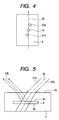
- FIG. 4 is a schematic illustration of the positional relationship of spot lights 1 a , 21 a and 22 a emitted from the respective laser beam sources 1 , 21 and 22 in the micro flow channel 6 .
- the arrow 30 of a broken line shows the locus of scanning of the spot light 1 a and the spot lights 21 a and 22 a are displaced oppositely relative to each other in the scanning direction of the spot light 1 a and in a direction perpendicular to that scanning direction and projected.
- FIG. 5 schematically illustrates how the laser beams emitted respectively from the laser beam sources 1 , 21 and 22 are reflected by the top surface and the bottom surface of a micro flow channel.
- the optical axes 1 b and 13 b show a relationship as described below. That is, the projection optical axis 1 b of excitation light from the laser beam source 1 and the imaging optical axis 13 b of light entering the light receiving section of the line sensor 13 intersect each other at a position between the flow channel top surface 6 a and the flow channel bottom surface 6 b of the micro flow channel 6 . In other words, the line sensor 13 receives only fluorescence emitted from the inside of the micro flow channel 6 .
- Excitation light excites the material of the substrate 4 all the way until getting to the flow channels 5 through 7 and after passing the flow channels 5 through 7 and the substrate 4 also emits auto-fluorescence.
- auto-fluorescence emitted at a position remote from the intersection with the imaging optical axis 13 b is projected onto a position displaced in a direction perpendicular to the direction of arrangement of the pixels of the line sensor 13 as viewed from the pixels so that auto-fluorescence of the substrate 4 is never received by the line sensor 13 as a signal. Therefore, the line sensor 13 detects only fluorescence emitted from the inside of the micro flow channel 6 that is the object of detection of the line sensor 13 . Thus, the line sensor 13 detects fluorescence with a good S/N ratio.
- the spot light 21 a irradiated from the laser beam source 21 is projected along the optical axis 21 b onto an eccentric position relative to the projection optical axis 1 b of excitation light on the top surface 4 a of the substrate 4 . Then, it proceeds toward the flow channel top surface 6 a . Since the refractive index of the material of the substrate 4 and that of the fluid in the flow channel 6 differ from each other, the spot light 21 a that is irradiated along the optical axis 21 b is partly reflected at the flow channel top surface 6 a .
- the first reflected light of the spot light 21 a that is reflected by the flow channel top surface 6 a is transmitted through the fluorescence filter 12 and led to the line sensor 13 by the focusing element array 11 .
- the reflection image 21 c of the spot light 21 a emitted from the laser beam source 21 that is formed on the flow channel top surface 6 a is eccentric in a direction perpendicular to the direction of arrangement of the pixels of the light receiving section 13 a of the line sensor 13 to such an extent that it partly lies on the line sensor 13 .
- the other spot light 22 a emitted from the laser beam source 22 also proceeds along the optical axis 22 b as illustrated in FIG. 5 and projected to a position eccentric relative to the optical axis 1 b at the side opposite to the optical axis 21 b .
- the spot light 22 a is partly reflected by the flow channel top surface 6 a just like the spot light 21 a that proceeds along the optical axis 21 b , the remaining part of the spot light 22 a is transmitted through the micro flow channel 6 and gets to the flow channel bottom surface 6 b . Since the refractive index of the material of the substrate 4 and that of the fluid in the flow channel 6 differ from each other, the spot light 22 a is also partly reflected at the flow channel bottom surface 6 b .
- the second reflected light that is part of the spot light 22 a reflected by the flow channel bottom surface 6 b is transmitted through the fluorescence filter 12 and projected onto the line sensor 13 by the focusing element array 11 .
- the reflection image 22 c of the spot light 22 a formed by the flow channel bottom surface 6 b is led to a position eccentric relative to the light receiving section 13 a at the side opposite to the reflection image 21 c as illustrated in FIG. 6 .
- the reflection image 22 c is projected to a position that is eccentric relative to the light receiving section 13 a of the line sensor 13 to such an extent that it partially lie thereon.
- the reflection image 22 c is projected to a position that is eccentric relative to the running direction of the line sensor 13 to such an extent that it does not lie on the reflection image 21 c formed by the spot light 21 a from the laser beam source 21 and the reflection image 1 c of excitation light from the laser beam source 1 .
- the reflection image at the flow channel bottom surface 6 b of the spot light 21 a proceeding along the optical axis 21 b and the reflection image at the flow channel top surface 6 a of the spot light 22 a proceeding along the optical axis 22 b are projected to respective positions that are far away from the light receiving section 13 a of the line sensor 13 than the reflection images 21 c and 22 c so that those reflection images are never recognized as signals by the line sensor 13 .
- FIG. 7 is a graph illustrating the outputs P from the pixels of the line sensor of FIG. 6 when the reflection images 1 c , 21 c and 22 c are received by the light receiving section 13 a of the line sensor 13 illustrated in FIG. 6 .
- reference symbols 1 d , 21 d and 22 d respectively denote the outputs P of the reflection images 1 c , 21 c and 22 c .
- the outputs P of the pixels of the light receiving region 13 a of the line sensor 13 at the focus positions of the reflection images 21 c and 22 c are substantially equal to each other as indicated by reference symbols 21 d and 22 d in FIG. 7 .
- FIG. 8 is a schematic illustration of a state where the substrate 4 and the micro flow channel 6 formed in it are moved to a position located closer to the spot light projecting section 101 and the imaging section 102 by distance 4 d from the position illustrated in FIG. 5 .
- the micro flow channel 6 shows a positional relationship as illustrated in FIG. 8 relative to the spot light projecting section 101 and the imaging section 102 (see FIG. 1 )
- the light beam emitted from the laser beam source 21 and proceeds along the optical axis 21 b is reflected at position 701 located close to the imaging optical axis 13 b on the flow channel top surface 6 a .
- the light beam that is emitted from the laser beam source 22 and proceeds along the optical axis 22 b is reflected at position 702 located remote from the imaging optical axis 13 b on the flow channel bottom surface 6 b .
- the reflection images 21 c and 22 c formed by the light beams that proceed respectively along these optical axes 21 b and 22 b show positional relationships relative to the light receiving section 13 a of the line sensor 13 as illustrated in FIG. 9 .
- the reflection image 21 c formed by the light beam coming from the laser beam source 21 is focused at a position close to the light receiving section 13 a of the line sensor 13
- the reflection image 22 c formed by the light beam coming from the laser beam source 22 is focused at a position remote from the light receiving section 13 a .
- the output 21 d from the pixel of the light receiving section 13 a of the line sensor 13 at the focus position of the reflection image 21 c is stronger than the output 22 d of the pixel at the focus position of the reflection image 22 c (see FIG. 10 ).
- FIG. 11 is a schematic illustration of a state where the substrate 4 and the micro flow channel 6 formed in it are moved to a position located far away from the spot light projecting section 101 and the imaging section 102 by the distance 4 e from the position illustrated in FIG. 5 .
- the micro flow channel 6 shows a positional relationship as illustrated in FIG. 11 relative to the spot light projecting section 101 and the imaging section 102 (see FIG. 1 )
- the light beam emitted from the laser beam source 21 and proceeds along the optical axis 21 b is reflected at position 1001 located remote from the imaging optical axis 13 b on the flow channel top surface 6 a .
- the light beam that is emitted from the laser beam source 22 and proceeds along the optical axis 22 b is reflected at position 1002 located close to the imaging optical axis 13 b on the flow channel bottom surface 6 b .
- the reflection images 21 c and 22 c formed by the light beams that proceed respectively along these optical axes 21 b and 22 b show positional relationships relative to the light receiving section 13 a of the line sensor 13 as illustrated in FIG. 12 .
- the reflection image 21 c formed by the light beam coming from the laser beam source 21 is focused at a position remote from the light receiving section 13 a of the line sensor 13
- the reflection image 22 c formed by the light beam coming from the laser beam source 22 is focused at a position close to the light receiving section 13 a .
- the output 21 d from the pixel of the light receiving section 13 a of the line sensor 13 at the focus position of the reflection image 21 c is weaker than the output 22 d of the pixel at the focus position of the reflection image 22 c (see FIG. 13 ).
- the distance between the spot light projecting section 101 and the imaging section 102 (see FIG. 1 ) and the micro flow channels 5 through 7 is so held that the intensities of the two reflection images 21 c and 22 c that are detected by the light receiving section 13 a of the line sensor 13 are substantially equal to each other.
- the line sensor 13 can constantly catch fluorescence emitted from the fluorescence label in the corresponding one of the flow channels 5 through 7 .
- FIG. 14 is a schematic illustration of the configuration of the line sensor illustrated in FIG. 1 .
- the light receiving section 13 a of the line sensor 13 is formed by a plurality of pixels c 1 , c 2 , c 3 , . . . that are photoelectric conversion elements such as photodiodes and has a function of accumulating the electric charges produced as a result of photoelectric conversions.
- the line sensor 13 additionally has a CCD 13 b for receiving the electric charges accumulated in the light receiving section 13 a according to a charge read indication signal and an amplifier 13 c for converting the accumulated electric charges of the pixels of the CCD 13 b into voltage values sequentially in the order of arrangement of the pixels according to a CCD transfer indication signal.
- the CCD 13 b receives the electric charges accumulated in the light receiving section 13 a according to the charge read indication signal. Subsequently, the electric charges accumulated in the CCD 13 b are sequentially output to the outside of the line sensor 13 by way of the amplifier 13 c for converting the accumulated electric charges into voltage values sequentially in the order of arrangement of the pixels of the CCD 13 b according to the CCD transfer indication signal.
- FIG. 14 also illustrates how the reflection images 1 c , 21 c and 22 c are virtually projected onto the pixels c 1 , c 2 , c 3 , . . . of the light receiving section 13 a of the line sensor 13 .
- the reflection images 1 c , 21 c and 22 c move in the direction of arrangement of the pixels according to the scanning operation of the scanning section 2 .
- FIG. 15 is a schematic illustration of the positions of spot lights projected into the micro flow channel 6 .
- a plurality of targets of detection 601 , 603 , 605 and 607 are arranged in the flow channel 6 with buffer solutions 602 , 604 and 606 interposed among them.
- the three spot lights move along the flow channel 6 in the rightward direction illustrated in FIG. 15 in response to the above-described scanning motion of the scanning section 2 .
- FIGS. 16A , 16 B and 16 C illustrate the waveforms of the signals read out at this time from the line sensor 13 .
- the horizontal axis indicates the position in the direction of arrangement of pixels of the line sensor 13 and the vertical axis indicates the intensity of the signal from each pixel.
- the signal waveform at time T 1 illustrated in FIG. 16A shows three peaks 1501 , 1502 and 1503 .
- the two peaks including the left peak 1501 and the right peak 1503 indicate the intensities of the reflection images 21 c and 22 c to be used for focus detection
- the central peak 1502 indicates the intensity of fluorescence coming from the inside of the flow channel 6 of the reflection image 1 c formed by excitation light.
- a high intensity of fluorescence is obtained at time T 1 because the excitation spot light 1 a irradiates the target of detection 601 .
- the detected intensity of fluorescence is weaker at time T 2 than at time T 1 because the excitation spot light 1 a irradiates a spot between the target of detection 601 and the buffer solution 602 at time T 2 .
- the central peak 1505 at time T 2 is lower than the central peak 1502 at time T 1 .
- the intensities of the left and right peaks 1504 and 1506 at time T 2 are not changed remarkably because they show the intensities of the reflection images from the flow channel top surface and the flow channel bottom surface respectively.
- the detected intensity of fluorescence (the height of the central peak 1508 ) is still weaker at time T 3 than at time T 2 because the excitation spot light 1 a irradiates the buffer solution 602 at time T 3 .
- FIG. 17 is a graph showing the relationship between the positions (horizontal axis) of pixels arranged in the line sensor 13 in the direction of arrangement thereof and the intensities of the signals (vertical axis) from the respective pixels.
- the dark circles in FIG. 17 represent the values obtained from the actual waveforms showing the intensities of the signals.
- the positions of the dark circles correspond to the positions of the peaks 1502 , 1505 and 1508 ( FIGS. 16A , 16 B and 16 C) showing the intensities of fluorescence. While the peaks are shown as those of curves in FIGS. 16A , 16 B and 16 C, they actually represent the peak outputs of the corresponding pixels of the line sensor as illustrated in FIG. 18 .
- the position of each of the peaks may be determined by using a threshold value that is about 20% of the peak of intensity of fluorescence and finding the center of gravity or the center of area of the waveform.
- the height of each of the dark circles represents the value obtained by adding the outputs of the pixels that constitute the waveform of the peak 1502 .
- the coordinates of the dark circles that are determined in this way are plotted to obtain T 1 , T 2 and T 3 in FIG. 17 .
- the other dark circles in FIG. 17 are also obtained from the actual waveforms.
- the electric charges of all the pixels of the line sensor 13 are read at a rate of 4 MHz.
- 2,000 sets of data each set showing a waveform as illustrated in any of FIGS. 16A , 16 B and 16 C, are obtained by a single main scanning operation.
- the defocusing direction (whether the spot light projecting section and the imaging section are approaching or moving away from the flow channel) can be detected by detecting the intensities of two peaks of focus detecting spot lights as focusing signals and comparing them on a real time basis.
- a constant intensity is obtained for the signals of two focus detecting spot lights regardless of the intensity of fluorescence produced by a spot light of excited light. Therefore, if the intensity of the central peak that represents the intensity of fluorescence produced by the spot light of excited light is low, the position of the central peak can be determined by using these signals. Since the position of the central peak is located between two focus detecting spot lights, it can be determined from the positions of the two focus detecting spot lights. Thus, an accurate image can be picked up because the peak position of signal intensity and hence the focus position can be accurately determined from the intensity signals obtained by using two focus detecting spot lights in the above-described manner.
- the above-described method reads signals from all the pixels of the line sensor 13 at regular time intervals and records them in a memory while scanning spot lights.
- components that show a high processing rate need to be used for the A/D conversion section 19 (see FIG. 1 ) and other components and a large capacity memory 17 (see FIG. 1 ) is required.
- the A/D conversion section does not show a high processing rate, it may alternatively be so arranged that approximate positions of the spot lights are stored in a memory in advance in order to scan the spot lights with a memory having a small capacity so as to take out the signals of only the pixels located around them. Such an arrangement can also acquire image information like the above-described method.
- the signal reading rate may be lowered to reduce the amount of data to be processed by detecting the angle of the scanning section 2 and reading information only on the pixels corresponding to the positions of the spot lights.
- FIG. 19 is a schematic illustration of an accumulated state of the electric charges of the pixels of the line sensor and an operation of reading out the electric charges from the pixels of the line sensor.
- pixels c 1 , c 2 , . . . , c 20 , . . . that are arranged sequentially in the line sensor are listed vertically, while the progress of time is horizontally indicated by t.
- the line sensor 13 of this embodiment is a CMOS sensor and the timing of reading the accumulated electric charge of each of the pixels thereof can be controlled externally.
- the main scanning angle of the scanning section 2 is detected and the electric charges of the charge accumulating pixels are sequentially read out in a switching manner in synchronism with the detected angle of the scanning section 2 .
- the CPU 18 detects the defocusing direction and makes necessary corrections by sequentially reading out data from the memory 17 and comparing the intensities of the two spot lights 21 c and 22 c . Since the durations of accumulation of electric charges varies as pointed out earlier, preferably the durations are detected so as to correct the intensity of fluorescence of the spot light 1 c.
- control circuit 16 compares the intensities of the first and second reflected lights (reflection images 21 c and 22 c ) and determines the direction and the quantity of deviation of each of the spot lights 1 a , 21 a and 22 a in the depth direction of the micro flow channel. Then, as will be described hereinafter, the focus position adjustment system is operated in response to the direction and the quantity of deviation to adjust the focus position of each of the spot lights 1 a , 21 a and 22 a.
- the focus position of each of the spot lights that are irradiated from the spot light projecting section 101 relative to any of the micro flow channels 5 through 7 in the substrate 4 can be adjusted by means of a focus position adjustment mechanism, which will be described below.
- a vertical drive mechanism (not shown) for driving the spot light projecting section 101 and the imaging section 102 , which are arranged in the cabinet 14 as illustrated in FIG. 1 , may be provided so as to move them in a direction perpendicular to the substrate 4 (in the depth direction of the micro flow channel). Then, the focus can be corrected by driving the spot light projecting section 101 and the imaging section 102 to move vertically so as to make the intensities of the two focus detecting reflection images 21 c and 22 c equal to each other. Note, however, that the spot light projecting section 101 and the imaging section 102 illustrated in FIG. 1 can be considerably heavy. Then, a large vertical drive mechanism may be required to drive them to move quickly.
- the focus can also be corrected by driving only the spot light projecting section 101 to move vertically or horizontally relative to the substrate 4 by means of a vertical drive mechanism (not illustrated) or the drive section 15 .
- a vertical drive mechanism not illustrated
- the load of the drive mechanism can be reduced to make it possible to correct the focus quickly because it is only necessary to drive the spot light projecting section 101 to move.
- means for scanning a spot light in the main scanning direction that is running along the longitudinal direction of the flow channels 5 through 7 of the substrate 4 and, at the same time, deflecting the spot light in the depth direction of the substrate 4 may be provided.
- the operation of focus correction can be conducted quickly without driving a large vertical drive mechanism when such a means is employed.
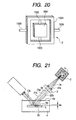
- FIG. 20 is a schematic perspective view of a scanning section that can deflect a spot light in the main scanning direction (the first direction) that is running along the longitudinal direction of the flow channels and also in the second direction that is perpendicular to the first direction on a plane running in parallel with the top surface and the bottom surface of the flow channels.
- the scanning section 2 illustrated in FIG. 20 has a mirror section 1501 that is rotatably supported by a frame member 1504 by means of first shafts 1502 and 1503 . Additionally, the frame member 1504 is rotatably supported by another frame member (not illustrated in FIG. 20 ) by means of second rotary shafts 1505 and 1506 that are orthogonal relative to the first shafts 1502 and 1503 .
- the mirror section 1501 is driven under control to swing in the sense of rotation around the first shafts 1502 and 1503 by known driven means so as to operate a spot light for main scanning.
- the frame member 1504 that supports the mirror section 1501 is driven to rotate under control around the second shafts 1505 and 1506 by a known drive means so as to deflect the spot light in the depth direction of the substrate 4 .
- the scanning section 2 is angularly controlled and driven to turn to a direction inclined by 90° from the main scanning direction for focus control as illustrated in FIG. 21 .
- the reflection image 21 c is located at a position remote from the light receiving section 13 a while the reflection image 22 c is located at a position close to the light receiving section 13 a as illustrated in FIG. 12 out of the spot lights that proceed along the optical axes 21 b and 22 b .
- the light beams emitted from the light beam sources 21 and 22 are deflected downwardly as indicated by reference symbols 21 e and 22 e by rotating the scanning section 2 in a direction perpendicular to the main scanning direction for adjustment as illustrated in FIG. 21 .
- the two reflection images of the light beams 21 e and 22 e can be formed at equidistant positions relative to the light receiving section 13 a of the line sensor 13 .
- the light beam that proceeds along the optical axis 1 e formed by the light beam emitted from the excitation light source 1 intersects the imaging optical axis 13 b at an intermediate position between the flow channel top surface 6 a and the flow channel bottom surface 6 b so that the line sensor 13 can efficiently catch the fluorescence image from the flow channel 6 .
- a fluorescence image of the fluorescence label in any of the flow channels can be efficiently picked up even if the flow channels 5 through 7 are displaced from the imaging plane formed by the imaging depth due to deformation or a manufacturing error on the part of the flow channels 5 through 7 .
- the depth of focus of such a focusing element array is generally 200 to 300 ⁇ m and the observed value of a reflection image is not affected by a displacement of tens of several ⁇ m.
- a technique of measuring the temperature of the surface of the substrate to estimate the temperature in the flow channel may be conceivable.
- the temperature of the surface of a substrate is apt to be influenced by the environment and hence cannot be measured accurately.
- the accuracy of detecting the intensity of fluorescence can be improved if it is possible to measure the temperature in the flow channel that changes incessantly along with fluorescence.
- the reflectance of the top surface and the bottom surface of a flow channel is determined by the refractive index of the material of the substrate and the refractive index of the fluid flowing in the inside of the flow channel.
- the refractive index of the fluid flowing in the inside of the flow channel varies as a function of temperature as illustrated FIG. 22 . Therefore, the temperature of the liquid in the flow channel can be determined from the intensity of light reflected by the top surface and the bottom surface of the flow channel.
- the memory 17 of the control circuit 16 stores the correlations of the temperature of the substrate 4 and that of the liquid flown in the flow channel thereof and the reflectance of light at the interfaces of the flow channel (the flow channel top surface 6 a and the flow channel bottom surface 6 b ) and the liquid at the temperatures.
- FIG. 23 is a graph where the horizontal axis indicates time T and the vertical axis indicates the intensities P of the reflection images 21 c and 22 c during a main scanning cycle.
- the reference symbols 21 f and 22 f denote the intensities of the respective reflection images that are formed as the laser beams emitted from the focus detecting laser beam sources 21 and 22 are reflected at the top surface and the bottom surface of the flow channel, while the broken line 1801 shows the average values thereof. While the intensities 21 f and 22 f may fluctuate individually due to defocusing, they are constantly equal if the positions of the reflection images 21 c and 22 c are shifted as long as the temperature is constant.
- the average intensity 1801 changes as the temperature of the liquid in the flow channel changes and the reflectance changes due to the changes in the refractive indexes as described above.
- the average intensity is high in the region indicated by reference symbol 1802 in FIG. 23 . This indicates that the reflectance is raised and hence the difference of refractive index between the substrate and the liquid is increased in and near the region. Then, it is seen that the refractive index of the liquid is made to fall and hence the temperature of the liquid is raised.
- the graph of the average intensities 1801 can also be obtained by smoothly linking the points where the two intensities 22 f and 21 f are equal to each other such as the points indicated by reference symbols 1802 , 1803 , 1804 and so on.
- the CPU 18 of the control circuit 16 determines the reflectance of light at the flow channel top surface and the flow channel bottom surface from the ratio of the average intensity 1801 relative to the intensities of the laser beams (the second spot lights) emitted from the focus detecting laser beam sources 21 and 22 . Note that information on the intensities of the laser beams emitted from the laser beam sources 21 and 22 is input to the control circuit 16 . Then, the CPU 18 of the control circuit 16 can determine the temperature of the liquid in the flow channel from the correlation of the reflectance and the liquid temperature stored in the memory 17 , using the obtained reflectance. The CPU 18 of the control circuit 16 can store the tendency of shift of the average value of the intensities of the two reflected light beams due to defocusing in advance and computationally determine the temperature of the liquid on the basis of the obtained values and the tendency.
- the light detecting (imaging) operation can alternatively be conducted by using an area sensor formed by two-dimensionally arranging image pickup elements.
- An area sensor is formed by arranging a plurality of line sensors and the above-described light detecting operation can be conducted by means of an area sensor and detecting light, using a particular line of the area sensor.
- the scanning imaging device has a control circuit 16 including a memory 17 , a CPU 18 and an A/D conversion section 19 as a control means and the control circuit 16 is connected to the scanning imaging device in the above description.
- the control circuit 16 may be replaced by an external computer (not illustrated) that operate as the memory 17 , the CPU 18 and the A/D conversion section 19 and the computer may be connected to the scanning imaging device. Then, the external computer operates as a control means with such an arrangement.
- a fluorescence label is added to the target of detection as light emitting label and fluorescence emitted from the fluorescence label is detected in the above description.
- a label that can be used as light emitting label is by no means limited to such a fluorescence label.
- a label adapted to emit phosphorescence may alternatively be added to the target of detection so as to detect phosphorescence emitted from the light emitting label.
Landscapes
- Physics & Mathematics (AREA)
- Health & Medical Sciences (AREA)
- General Physics & Mathematics (AREA)
- Chemical & Material Sciences (AREA)
- Nuclear Medicine, Radiotherapy & Molecular Imaging (AREA)
- Life Sciences & Earth Sciences (AREA)
- Optics & Photonics (AREA)
- Analytical Chemistry (AREA)
- Biochemistry (AREA)
- General Health & Medical Sciences (AREA)
- Immunology (AREA)
- Pathology (AREA)
- Investigating, Analyzing Materials By Fluorescence Or Luminescence (AREA)
Applications Claiming Priority (3)
| Application Number | Priority Date | Filing Date | Title |
|---|---|---|---|
| JP2008-096145 | 2008-04-02 | ||
| JP2008096145A JP5072688B2 (ja) | 2008-04-02 | 2008-04-02 | 走査型撮像装置 |
| PCT/JP2009/057234 WO2009123359A1 (fr) | 2008-04-02 | 2009-04-02 | Dispositif d'imagerie par balayage |
Publications (2)
| Publication Number | Publication Date |
|---|---|
| US20100230580A1 US20100230580A1 (en) | 2010-09-16 |
| US8716641B2 true US8716641B2 (en) | 2014-05-06 |
Family
ID=41135703
Family Applications (1)
| Application Number | Title | Priority Date | Filing Date |
|---|---|---|---|
| US12/744,575 Expired - Fee Related US8716641B2 (en) | 2008-04-02 | 2009-04-02 | Scanning imaging device for imaging target on a substrate |
Country Status (6)
| Country | Link |
|---|---|
| US (1) | US8716641B2 (fr) |
| EP (1) | EP2263074A4 (fr) |
| JP (1) | JP5072688B2 (fr) |
| KR (1) | KR101260290B1 (fr) |
| CN (1) | CN101981437B (fr) |
| WO (1) | WO2009123359A1 (fr) |
Cited By (2)
| Publication number | Priority date | Publication date | Assignee | Title |
|---|---|---|---|---|
| US10534975B1 (en) * | 2018-07-10 | 2020-01-14 | Kuan-Yu Lu | Multi-frequency high-precision object recognition method |
| US11921205B2 (en) | 2020-11-24 | 2024-03-05 | Pixart Imaging Inc. | Method for eliminating misjudgment of reflective lights and optical sensing system |
Families Citing this family (13)
| Publication number | Priority date | Publication date | Assignee | Title |
|---|---|---|---|---|
| WO2011085728A1 (fr) * | 2010-01-13 | 2011-07-21 | Flowsion Aps | Système micro-fluidique comprenant un dispositif d'émission de lumière |
| EP2461184B1 (fr) * | 2010-12-03 | 2015-07-08 | Agfa HealthCare N.V. | Dispositif et procédé destinés à l'extraction d'informations radiographiques stockées sur un disque fluorescent de mémoire |
| WO2015008435A1 (fr) * | 2013-07-17 | 2015-01-22 | パナソニックIpマネジメント株式会社 | Spectroscope |
| DE102014017490A1 (de) * | 2014-11-27 | 2016-06-02 | Jenoptik Optical Systems Gmbh | Vorrichtung und Verfahren zum Erfassen eines Inhaltes eines mit einer Flüssigkeit und/oder einem Granulat befüllbaren Behälters und/oder zur Erfassung der Größe eines befüllbaren Behälters, Befülleinrichtung zum Befüllen eines Behälters mit einer Flüssigkeit und/oder einem Granulat und Verwenden von Strahlung einer Reflexionslichtschranke zum Erfassen eines Füllstands einer Flüssigkeit und/oder eines Granulate in einem Behälter .... |
| US10799998B2 (en) * | 2016-10-17 | 2020-10-13 | Virtek Vision International Ulc | Laser projector with flash alignment |
| CN106530343A (zh) * | 2016-10-18 | 2017-03-22 | 深圳奥比中光科技有限公司 | 一种基于目标深度图像的投影装置和投影方法 |
| CN109426355B (zh) * | 2017-08-31 | 2022-12-30 | 华为终端有限公司 | 一种电子设备的输入方法、输入装置及电子设备 |
| EP3470924A1 (fr) * | 2017-10-11 | 2019-04-17 | ASML Netherlands B.V. | Procédé d'optimisation de la position et/ou de la taille d'un point d'éclairage de mesure par rapport à une cible sur un substrat et appareil associé |
| JP7062518B2 (ja) * | 2018-05-25 | 2022-05-06 | 株式会社キーエンス | 共焦点変位計 |
| JP7098146B2 (ja) * | 2018-07-05 | 2022-07-11 | 株式会社Iddk | 顕微観察装置、蛍光検出器及び顕微観察方法 |
| EP3927299B1 (fr) * | 2019-02-19 | 2023-03-08 | Alcon Inc. | Étalonnage de la position du point focal d'un faisceau laser |
| CN110017783B (zh) * | 2019-05-20 | 2023-09-29 | 广东理工学院 | 板件位移在线检测装置及传送系统 |
| US11826906B2 (en) * | 2020-11-24 | 2023-11-28 | Pixart Imaging Inc. | Method for eliminating misjudgment of reflective light and optical sensing system |
Citations (17)
| Publication number | Priority date | Publication date | Assignee | Title |
|---|---|---|---|---|
| JP2001108684A (ja) | 1999-10-05 | 2001-04-20 | Hitachi Ltd | Dna検査方法及びdna検査装置 |
| JP2001242081A (ja) | 2000-02-29 | 2001-09-07 | Nikon Corp | Dnaチップ読み取りヘッド及びdnaチップ読み取り装置 |
| WO2001073417A1 (fr) | 2000-03-27 | 2001-10-04 | Caliper Technologies Corp. | Procedes et systemes d'analyses microfluidiques a tres haut rendement |
| WO2003083459A1 (fr) | 2002-03-29 | 2003-10-09 | Otsuka Electronics Co., Ltd. | Appareil de mesure a fluorescence |
| US20030197112A1 (en) * | 1999-10-21 | 2003-10-23 | 3M Innovative Properties Company | Autofocus z stage |
| WO2003100474A2 (fr) | 2002-05-28 | 2003-12-04 | Autogenomics, Inc. | Detecteur de microreseaux et procedes associes |
| WO2003100389A1 (fr) | 2002-05-28 | 2003-12-04 | Autogenomics, Inc. | Ensemble de reactifs multiples |
| JP2004233114A (ja) | 2003-01-29 | 2004-08-19 | Fuji Electric Holdings Co Ltd | 抗原の分離装置並びにこれを利用した抗原の計測方法及び装置 |
| JP2005091134A (ja) | 2003-09-17 | 2005-04-07 | Matsushita Electric Ind Co Ltd | 蛍光読み取り装置及び蛍光読み取り装置の合焦点方法 |
| US6885454B2 (en) * | 2001-03-28 | 2005-04-26 | Fuji Photo Film Co., Ltd. | Measuring apparatus |
| US20050118640A1 (en) * | 2002-05-28 | 2005-06-02 | Fareed Kureshy | Microarray detector and methods |
| US20050121596A1 (en) * | 2002-03-13 | 2005-06-09 | Yeda Research And Development Company Ltd. | Auto-focusing method and device |
| US20060146910A1 (en) * | 2004-11-23 | 2006-07-06 | Manoochehr Koochesfahani | Method and apparatus for simultaneous velocity and temperature measurements in fluid flow |
| JP2006322707A (ja) | 2005-05-17 | 2006-11-30 | Funai Electric Co Ltd | 蛍光検出装置および検査チップ |
| JP2006349501A (ja) | 2005-06-16 | 2006-12-28 | Matsushita Electric Ind Co Ltd | 生体サンプル判別装置 |
| US7217573B1 (en) | 1999-10-05 | 2007-05-15 | Hitachi, Ltd. | Method of inspecting a DNA chip |
| US7504647B2 (en) * | 2003-11-18 | 2009-03-17 | Applied Materials, Inc. | Method and apparatus for inspecting a sample having a controller for determining an estimated height of the detector from the sample |
Family Cites Families (8)
| Publication number | Priority date | Publication date | Assignee | Title |
|---|---|---|---|---|
| JPS52106324A (en) | 1976-03-04 | 1977-09-06 | Kubota Ltd | Mold forming for hollow casting |
| DE19916749B4 (de) * | 1999-04-14 | 2004-02-12 | Carl Zeiss Jena Gmbh | Verfahren zur Untersuchung von Proben |
| US20020139936A1 (en) * | 2000-10-27 | 2002-10-03 | Dumas David P. | Apparatus for fluorescence detection on arrays |
| CN1137400C (zh) * | 2001-08-23 | 2004-02-04 | 华中科技大学 | 快速进行纵深扫描成像方法 |
| US8351026B2 (en) * | 2005-04-22 | 2013-01-08 | Affymetrix, Inc. | Methods and devices for reading microarrays |
| US7329860B2 (en) * | 2005-11-23 | 2008-02-12 | Illumina, Inc. | Confocal imaging methods and apparatus |
| EP2018622B1 (fr) | 2006-03-31 | 2018-04-25 | Illumina, Inc. | Systèmes pour analyse de séquençage par synthèse |
| US8048626B2 (en) * | 2006-07-28 | 2011-11-01 | California Institute Of Technology | Multiplex Q-PCR arrays |
-
2008
- 2008-04-02 JP JP2008096145A patent/JP5072688B2/ja not_active Expired - Fee Related
-
2009
- 2009-04-02 WO PCT/JP2009/057234 patent/WO2009123359A1/fr active Application Filing
- 2009-04-02 US US12/744,575 patent/US8716641B2/en not_active Expired - Fee Related
- 2009-04-02 EP EP09727267.8A patent/EP2263074A4/fr not_active Withdrawn
- 2009-04-02 KR KR1020107023856A patent/KR101260290B1/ko active IP Right Grant
- 2009-04-02 CN CN2009801109314A patent/CN101981437B/zh not_active Expired - Fee Related
Patent Citations (21)
| Publication number | Priority date | Publication date | Assignee | Title |
|---|---|---|---|---|
| US7217573B1 (en) | 1999-10-05 | 2007-05-15 | Hitachi, Ltd. | Method of inspecting a DNA chip |
| JP2001108684A (ja) | 1999-10-05 | 2001-04-20 | Hitachi Ltd | Dna検査方法及びdna検査装置 |
| JP3551860B2 (ja) | 1999-10-05 | 2004-08-11 | 株式会社日立製作所 | Dna検査方法及びdna検査装置 |
| US20030197112A1 (en) * | 1999-10-21 | 2003-10-23 | 3M Innovative Properties Company | Autofocus z stage |
| JP2001242081A (ja) | 2000-02-29 | 2001-09-07 | Nikon Corp | Dnaチップ読み取りヘッド及びdnaチップ読み取り装置 |
| WO2001073417A1 (fr) | 2000-03-27 | 2001-10-04 | Caliper Technologies Corp. | Procedes et systemes d'analyses microfluidiques a tres haut rendement |
| JP2003529076A (ja) | 2000-03-27 | 2003-09-30 | カリパー・テクノロジーズ・コープ. | 超高処理量ミクロ流体分析システム及び方法 |
| US6885454B2 (en) * | 2001-03-28 | 2005-04-26 | Fuji Photo Film Co., Ltd. | Measuring apparatus |
| US20050121596A1 (en) * | 2002-03-13 | 2005-06-09 | Yeda Research And Development Company Ltd. | Auto-focusing method and device |
| WO2003083459A1 (fr) | 2002-03-29 | 2003-10-09 | Otsuka Electronics Co., Ltd. | Appareil de mesure a fluorescence |
| JP2003294633A (ja) | 2002-03-29 | 2003-10-15 | Otsuka Denshi Co Ltd | 蛍光測定装置 |
| JP2005527827A (ja) | 2002-05-28 | 2005-09-15 | オウトジエノミクス・インコーポレーテツド | マイクロアレイ検出器および方法 |
| US20050118640A1 (en) * | 2002-05-28 | 2005-06-02 | Fareed Kureshy | Microarray detector and methods |
| WO2003100389A1 (fr) | 2002-05-28 | 2003-12-04 | Autogenomics, Inc. | Ensemble de reactifs multiples |
| WO2003100474A2 (fr) | 2002-05-28 | 2003-12-04 | Autogenomics, Inc. | Detecteur de microreseaux et procedes associes |
| JP2004233114A (ja) | 2003-01-29 | 2004-08-19 | Fuji Electric Holdings Co Ltd | 抗原の分離装置並びにこれを利用した抗原の計測方法及び装置 |
| JP2005091134A (ja) | 2003-09-17 | 2005-04-07 | Matsushita Electric Ind Co Ltd | 蛍光読み取り装置及び蛍光読み取り装置の合焦点方法 |
| US7504647B2 (en) * | 2003-11-18 | 2009-03-17 | Applied Materials, Inc. | Method and apparatus for inspecting a sample having a controller for determining an estimated height of the detector from the sample |
| US20060146910A1 (en) * | 2004-11-23 | 2006-07-06 | Manoochehr Koochesfahani | Method and apparatus for simultaneous velocity and temperature measurements in fluid flow |
| JP2006322707A (ja) | 2005-05-17 | 2006-11-30 | Funai Electric Co Ltd | 蛍光検出装置および検査チップ |
| JP2006349501A (ja) | 2005-06-16 | 2006-12-28 | Matsushita Electric Ind Co Ltd | 生体サンプル判別装置 |
Non-Patent Citations (2)
| Title |
|---|
| Office Action in Chinese Application No. 200980110931.4 (Nov. 25, 2011). |
| Office Action in Korean Application No. 10-2010-7023856 (Jun. 19, 2012). |
Cited By (2)
| Publication number | Priority date | Publication date | Assignee | Title |
|---|---|---|---|---|
| US10534975B1 (en) * | 2018-07-10 | 2020-01-14 | Kuan-Yu Lu | Multi-frequency high-precision object recognition method |
| US11921205B2 (en) | 2020-11-24 | 2024-03-05 | Pixart Imaging Inc. | Method for eliminating misjudgment of reflective lights and optical sensing system |
Also Published As
| Publication number | Publication date |
|---|---|
| CN101981437B (zh) | 2013-08-28 |
| US20100230580A1 (en) | 2010-09-16 |
| KR20100139077A (ko) | 2010-12-31 |
| EP2263074A1 (fr) | 2010-12-22 |
| JP5072688B2 (ja) | 2012-11-14 |
| CN101981437A (zh) | 2011-02-23 |
| JP2009250671A (ja) | 2009-10-29 |
| KR101260290B1 (ko) | 2013-05-07 |
| WO2009123359A1 (fr) | 2009-10-08 |
| EP2263074A4 (fr) | 2017-08-30 |
Similar Documents
| Publication | Publication Date | Title |
|---|---|---|
| US8716641B2 (en) | Scanning imaging device for imaging target on a substrate | |
| US8686376B2 (en) | Microarray characterization system and method | |
| US6586750B2 (en) | High performance substrate scanning | |
| US7911670B2 (en) | Fluorescence-based scanning imaging device | |
| JP4812393B2 (ja) | 蛍光分子計測システム | |
| EP1209461B1 (fr) | Procédé pour la lecture de la fluorescence | |
| JP4495083B2 (ja) | 蛍光相関分光解析装置 | |
| KR20120036230A (ko) | 형광 검출 광학계 및 이를 포함하는 다채널 형광 검출 장치 | |
| US6630680B2 (en) | Scanner having confocal optical system, method for producing focus position data of confocal optical system of scanner having confocal optical system and method for producing digital data of scanner having confocal optical system | |
| JP2011504247A (ja) | オートフォーカス付き光学的コード走査装置 | |
| KR101224600B1 (ko) | 바이오칩 검출장치 | |
| WO2008010120A2 (fr) | Balayage d'un faisceau appliqué à la détection optique | |
| JP2019136023A (ja) | 細菌検出装置及び細菌検出方法 | |
| JP5164713B2 (ja) | 検出装置及び方法 | |
| JP2008039605A (ja) | 蛍光検出装置 | |
| JP2004354344A (ja) | 光源装置及びその光源装置が適用される生体分子解析装置 | |
| RU188251U1 (ru) | Устройство для сканирования биочипов | |
| US20040224421A1 (en) | Bi-directional scanning method | |
| CN117991488A (zh) | 成像系统、测序系统和成像方法 | |
| JP2000184140A (ja) | 走査開始点検出方法および走査装置、並びに画像情報読取方法および画像情報読取装置 | |
| JP2005257313A (ja) | 蛍光読取装置 | |
| AU5741800A (en) | Bi-directional scanning method | |
| JP2010066285A (ja) | 走査型光検出装置 |
Legal Events
| Date | Code | Title | Description |
|---|---|---|---|
| AS | Assignment |
Owner name: CANON KABUSHIKI KAISHA, JAPAN Free format text: ASSIGNMENT OF ASSIGNORS INTEREST;ASSIGNOR:MATSUMOTO, KAZUHIRO;REEL/FRAME:024757/0050 Effective date: 20100511 |
|
| STCF | Information on status: patent grant |
Free format text: PATENTED CASE |
|
| MAFP | Maintenance fee payment |
Free format text: PAYMENT OF MAINTENANCE FEE, 4TH YEAR, LARGE ENTITY (ORIGINAL EVENT CODE: M1551) Year of fee payment: 4 |
|
| LAPS | Lapse for failure to pay maintenance fees |
Free format text: PATENT EXPIRED FOR FAILURE TO PAY MAINTENANCE FEES (ORIGINAL EVENT CODE: EXP.); ENTITY STATUS OF PATENT OWNER: LARGE ENTITY |
|
| FEPP | Fee payment procedure |
Free format text: MAINTENANCE FEE REMINDER MAILED (ORIGINAL EVENT CODE: REM.); ENTITY STATUS OF PATENT OWNER: LARGE ENTITY |
|
| STCH | Information on status: patent discontinuation |
Free format text: PATENT EXPIRED DUE TO NONPAYMENT OF MAINTENANCE FEES UNDER 37 CFR 1.362 |
|
| FP | Lapsed due to failure to pay maintenance fee |
Effective date: 20220506 |