US8633137B2 - High-temperature superconducting tape - Google Patents
High-temperature superconducting tape Download PDFInfo
- Publication number
- US8633137B2 US8633137B2 US13/226,678 US201113226678A US8633137B2 US 8633137 B2 US8633137 B2 US 8633137B2 US 201113226678 A US201113226678 A US 201113226678A US 8633137 B2 US8633137 B2 US 8633137B2
- Authority
- US
- United States
- Prior art keywords
- temperature superconducting
- substrate
- layer
- superconducting tape
- superconducting layer
- Prior art date
- Legal status (The legal status is an assumption and is not a legal conclusion. Google has not performed a legal analysis and makes no representation as to the accuracy of the status listed.)
- Active, expires
Links
Images


Classifications
-
- H—ELECTRICITY
- H01—ELECTRIC ELEMENTS
- H01B—CABLES; CONDUCTORS; INSULATORS; SELECTION OF MATERIALS FOR THEIR CONDUCTIVE, INSULATING OR DIELECTRIC PROPERTIES
- H01B12/00—Superconductive or hyperconductive conductors, cables, or transmission lines
- H01B12/02—Superconductive or hyperconductive conductors, cables, or transmission lines characterised by their form
- H01B12/06—Films or wires on bases or cores
-
- H—ELECTRICITY
- H10—SEMICONDUCTOR DEVICES; ELECTRIC SOLID-STATE DEVICES NOT OTHERWISE PROVIDED FOR
- H10N—ELECTRIC SOLID-STATE DEVICES NOT OTHERWISE PROVIDED FOR
- H10N60/00—Superconducting devices
- H10N60/01—Manufacture or treatment
- H10N60/0268—Manufacture or treatment of devices comprising copper oxide
- H10N60/0296—Processes for depositing or forming superconductor layers
- H10N60/0576—Processes for depositing or forming superconductor layers characterised by the substrate
- H10N60/0632—Intermediate layers, e.g. for growth control
Definitions
- the present invention relates to a high-temperature superconducting tape, and, more particularly, to a high-temperature superconducting tape, the critical current characteristics of which are improved because a stainless steel substrate, which is advantageous to electropolishing, is used and because of adjusting the composition ratio and crystal grain size of the stainless steel substrate.
- a high-temperature superconducting tape is manufactured by depositing a superconducting layer, such as YBCO, on a flexible metal substrate.
- a superconducting layer such as YBCO
- YBCO a superconducting layer
- the superconducting critical temperature and critical current density of YBCO tend to decrease, so that it is required to form a buffer layer, serving as a diffusion barrier, between the YBCO superconducting layer and the metal substrate.
- Ni nickel (Ni), which is contained in the metal substrate in large quantity, is diffused into YBCO lattices, the superconducting characteristics of YBCO are rapidly deteriorated, so that it is required to prevent nickel (Ni) from being diffused into the YBCO superconducting layer using the buffer layer formed between the metal substrate and the YBCO superconducting layer.
- the buffer layer is formed between a metal substrate and a superconducting layer to chemically separate the superconducting layer from the metal substrate.
- the buffer layer is formed of a plurality of layers (diffusion barrier layer/seed layer/IBAD template/homogeneous epitaxial buffer layer/lattice-matched buffer layer) which are used to induce YBCO to be biaxially oriented.
- a diffusion barrier layer has been made of alumina (Al 2 O 3 ).
- alumina Al 2 O 3
- Such a diffusion barrier layer made of alumina is problematic in that, although the diffusion of metal components of a metal substrate into a superconducting layer can be prevented to some degree, the diffusion of the metal components into the superconducting layer with crystal grains cannot be completely prevented. Further, this diffusion barrier layer is problematic in that, since its surface roughness is not good, it is required to make a template relatively thick in order to deposit a high-grade superconducting layer on a metal substrate, and thus it takes a lot of time to manufacture a superconducting tape.
- stainless steel substrates are advantageous compared to conventional hastelloy substrates in that they are cheaper than the hastelloy substrates by 1/10 or less and they exhibit nonmagnetic properties, and in that they are easily electropolished to have low surface roughness, thus decreasing the thickness of a buffer layer (template) necessary for depositing a high-grade superconducting layer on a metal substrate. Therefore, recently, the research into stainless steel substrates (U.S. Pat. No. 6,541,121 B2, EP0312015) has been actively done.
- an object of the present invention is to provide a high-temperature superconducting tape, the critical current characteristics of which are improved because a stainless steel substrate, which is easily electropolished, is used and because of adjusting the composition ratio and crystal grain size of the stainless steel substrate.
- ReBCO ReBa 2 Cu 3 O 7
- the buffer layer may be made of yttrium oxide (Y 2 O 3 )/magnesia (MgO)/lanthanum manganate (LaMnO 3 ) or alumina (Al 2 O 3 )/yttrium oxide (Y 2 O 3 )/magnesia (MgO)/ceria (CeO 2 ).
- FIG. 1 shows electron microscope photographs of a substrate before and after electropolishing according to an embodiment of the present invention
- FIG. 2 is an electron microscope photograph showing the surface roughness of the substrate according to an embodiment of the present invention.
- FIG. 3 is a graph showing the data about the magnetic properties of the substrate according to an embodiment of the present invention.
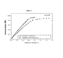
- FIG. 4 is a graph showing the data about the physical properties of a high-temperature superconducting tape when a conventional hastelloy substrate was used and when the substrate according to an embodiment of the present invention was used (in this case, a high-temperature superconducting layer made of gadolinium barium copper oxide (GdBa 2 Cu 3 O 7 , GBCO) was used);
- a high-temperature superconducting layer made of gadolinium barium copper oxide (GdBa 2 Cu 3 O 7 , GBCO) was used
- FIG. 5 is a graph showing the data about the critical current density of the high-temperature superconducting tape of the present invention (high-temperature superconducting tape of FIG. 4 );
- FIG. 6 is a photograph showing the state of the high-temperature superconducting tape when a conventional stainless steel substrate disclosed in U.S. Pat. No. 6,541,121 B2 was used.
- the present invention provides a high-temperature superconducting tape, including a substrate, a buffer layer formed on the substrate, and a high-temperature superconducting layer formed on the buffer layer.
- the substrate is made of SUS310s or stainless steel containing 0.01-1% of silicon (Si) and 1-5% of molybdenum (Mo) and has an average metal crystal grain size of 12 ⁇ m or less
- the substrate exhibits nonmagnetic properties and is inexpensive compared to a conventional hastelloy substrate, and is easily electropolished compared to a conventional stainless steel substrate, so that the surface roughness thereof is low and thus the thickness of a buffer layer can be reduced, with the result that a high-grade superconducting layer can be deposited on the thin buffer layer and thus the critical current density of the high-temperature superconducting tape can be improved, thereby remarkably improving the characteristics of the high-temperature superconducting tape.
- a SUS310s substrate or a stainless steel substrate including or silicon (Si) 0.5%, molybdenum (Mo) 1%, iron (Fe) 50%, nickel (Ni) 18%, chromium (Cr) 24%, manganese (Mn) 1.5% and residual carbon (C), and having an average metal crystal grain size of 8 ⁇ m was used.
- the amount of silicon is 0.01-1% by weight based on the total amount of the stainless steel substrate.
- the amount of silicon is less than 0.01%, there is a problem in that a Fe—Cr compound for improving the strength of stainless steel is scarcely precipitated.
- the amount thereof is more than 1%, the Fe—Cr compound is excessively precipitated, there is a problem in that the substrate is difficult to be electropolished, and becomes brittle. Therefore, it is preferred that the amount of silicon be 0.01-1%, because the strength and electropolishing ability of the substrate are improved within this range.
- 1-5% of molybdenum is added, the formation rate of the Fe—Cr compound is adjusted, thus improving both the strength and electropolishing ability of the substrate.
- the average metal crystal grain size of the substrate must be 12 ⁇ m or less.
- the average metal crystal grain size thereof is more than 12 ⁇ m, there is a problem in that the diffusion rate of the metal components of the substrate excessively increases. Therefore, the average metal crystal grain size thereof must be 12 ⁇ m or less. In this case, the average metal crystal grain size thereof can be adjusted by rolling and heat treatment. Further, when the average metal crystal grain size thereof is more than 12 ⁇ m, there are problems in that the high-temperature strength of the substrate is lowered, and in that the substrate is overetched during the electropolishing process.
- the buffer layer which is formed on the stainless steel substrate, is made of yttrium oxide (Y 2 O 3 )/magnesia (MgO)/lanthanum manganate (LaMnO 3 ) or alumina (Al 2 O 3 )/yttrium oxide (Y 2 O 3 )/magnesia (MgO)/ceria (CeO 2 ).
- the buffer layer made of alumina (Al 2 O 3 )/yttrium oxide (Y 2 O 3 )/magnesia (MgO)/ceria (CeO 2 ) was used, and this buffer layer can be formed by commonly-known thin-film deposition methods.
- the buffer layer is formed to a thickness of 100 nm by electron beam deposition and sputtering.
- the high-temperature superconducting layer is formed on the buffer layer, and is made of gadolinium barium copper oxide superconductor (GdBa 2 Cu 3 O 7 , GBCO) or samarium barium copper oxide superconductor (SmBa 2 Cu 3 O 7 , SmBCO).
- the high-temperature superconducting layer is formed to a thickness of 1-2 ⁇ m using co-evaporation.
- FIG. 1 shows electron microscope photographs of a substrate before and after electropolishing according to an embodiment of the present invention.
- the substrate of the present invention is advantageous to electropolishing, the surface roughness of the substrate is improved, so that the thickness of the buffer layer and high-temperature superconducting layer sequentially formed on the substrate can be decreased, and the characteristics of the superconducting tape can be improved by improving the critical current density thereof.
- FIG. 2 is an electron microscope photograph showing the surface roughness of the substrate according to an embodiment of the present invention. As shown in FIG. 2 , it can be ascertained that the average surface roughness of the substrate in the area of 10 ⁇ m ⁇ 10 ⁇ m is 2.0 nm or less, and thus the substrate is advantageous to electropolishing. Most of conventional hastelloy substrates have a surface roughness of 2.0 nm due to grain-boundary products produced during electropolishing.
- FIG. 3 is a graph showing the data about the magnetic properties of the substrate according to an embodiment of the present invention. As shown in FIG. 3 , it can be seen that the substrate nearly exhibit nonmagnetic properties at a temperature of 77K.
- FIG. 4 is a graph showing the data about the physical properties of a high-temperature superconducting tape when a conventional hastelloy substrate was used and when the substrate according to an embodiment of the present invention was used (in this case, a high-temperature superconducting layer made of gadolinium barium copper oxide (GdBa 2 Cu 3 O 7 , GBCO) was used). As shown in FIG.
- the elastic modulus of the high-temperature superconducting tape using the stainless steel substrate of the present invention at 77K is 143.6 GPa
- the elastic modulus of the high-temperature superconducting tape using the conventional hastelloy substrate at 77K is 114.3 GPa
- both the yield strength of the substrate of the present invention and the yield strength of the conventional hastelloy substrate are 800 MPa or more.
- FIG. 5 is a graph showing the data about the critical current density of the high-temperature superconducting tape of the present invention (high-temperature superconducting tape of FIG. 4 ). From FIG. 5 , it can be observed that the critical current density of the high-temperature superconducting tape using the stainless steel substrate of the present invention is similar to or higher than that of the high-temperature superconducting tape using the conventional hastelloy substrate. That is, when the conventional hastelloy substrate was used, the critical current density thereof was 450 A.
- the critical current density thereof was 575 A (a SUS310S substrate was used as the substrate, SUS 1) or 475 A (a stainless steel substrate including silicon (Si) 0.5%, molybdenum (Mo) 1%, iron (Fe) 50%, nickel (Ni) 18%, chromium (Cr) 24%, manganese (Mn) 1.5% and residual carbon (C), SUS 2). Consequently, it can be ascertained that the critical current density of the high-temperature superconducting tape using the stainless steel substrate of the present invention is superior to that of the high-temperature superconducting tape using the conventional hastelloy substrate.
- FIG. 6 is a photograph showing the state of the conventional high-temperature superconducting tape which was manufactured by sequentially forming a buffer layer and a superconducting layer on a conventional stainless steel substrate disclosed in U.S. Pat. No. 6,541,121 B2 in the same manner as an embodiment of the present invention and then applying silver (Ag) thereonto to form a protective layer.
- the surface roughness of this conventional high-temperature superconducting tape is higher than that of the high-temperature superconducting tape of the present invention, and, in this case, the silver (Ag) protective layer is easily damaged, thus deteriorating the overall characteristics of the high-temperature superconducting tape.
- the stainless steel substrate is advantageous to electropolishing, the surface roughness thereof is lowered, so that the thickness of the buffer layer or superconducting layer can be reduced and the critical current density of the high-temperature superconducting tape can be improved, thereby improving the overall characteristics of the high-temperature superconducting tape and reducing the manufacturing cost of the high-temperature superconducting tape.
- the high-temperature superconducting tape according to the present invention is advantageous in that a stainless steel substrate obtained by adjusting the composition ratio and metal grain size of the substrate exhibits nonmagnetic properties and is inexpensive compared to a conventional hastelloy substrate, and is easily electropolished compared to a conventional stainless steel substrate, so that the surface roughness thereof is low and thus the thickness of a buffer layer can be reduced, with the result that a high-grade superconducting layer can be deposited on the thin buffer layer and thus the critical current density of the high-temperature superconducting tape can be improved, thereby remarkably improving the characteristics of the high-temperature superconducting tape.
Applications Claiming Priority (2)
| Application Number | Priority Date | Filing Date | Title |
|---|---|---|---|
| KR1020110029468A KR20120111137A (ko) | 2011-03-31 | 2011-03-31 | 고온 초전도 선재 |
| KR10-2011-0029468 | 2011-03-31 |
Publications (2)
| Publication Number | Publication Date |
|---|---|
| US20120252680A1 US20120252680A1 (en) | 2012-10-04 |
| US8633137B2 true US8633137B2 (en) | 2014-01-21 |
Family
ID=45562079
Family Applications (1)
| Application Number | Title | Priority Date | Filing Date |
|---|---|---|---|
| US13/226,678 Active 2031-10-21 US8633137B2 (en) | 2011-03-31 | 2011-09-07 | High-temperature superconducting tape |
Country Status (5)
| Country | Link |
|---|---|
| US (1) | US8633137B2 (ko) |
| EP (1) | EP2506324B1 (ko) |
| JP (1) | JP5492159B2 (ko) |
| KR (1) | KR20120111137A (ko) |
| ES (1) | ES2537443T3 (ko) |
Families Citing this family (4)
| Publication number | Priority date | Publication date | Assignee | Title |
|---|---|---|---|---|
| US11309480B2 (en) | 2015-05-11 | 2022-04-19 | University Of Houston System | Ultra-thin film superconducting tapes |
| EP3282493B1 (de) * | 2016-08-10 | 2020-03-11 | Theva Dünnschichttechnik GmbH | Hochtemperatur-supraleiter-bandleiter mit edelstahl-substrat |
| CN108963067B (zh) * | 2018-07-27 | 2022-04-29 | 武汉工程大学 | 一种ReBa2Cu3O7-x超导薄膜上制备钉扎层的方法 |
| CN113013318B (zh) * | 2021-03-09 | 2023-07-11 | 傲普(上海)新能源有限公司 | 一种储能用高温超导材料性能提高方法 |
Citations (5)
| Publication number | Priority date | Publication date | Assignee | Title |
|---|---|---|---|---|
| US4994435A (en) * | 1987-10-16 | 1991-02-19 | The Furukawa Electric Co., Ltd. | Laminated layers of a substrate, noble metal, and interlayer underneath an oxide superconductor |
| US5019555A (en) * | 1988-08-10 | 1991-05-28 | General Atomics | High purity superconducting compositions and methods for their fabrication |
| US5964966A (en) * | 1997-09-19 | 1999-10-12 | Lockheed Martin Energy Research Corporation | Method of forming biaxially textured alloy substrates and devices thereon |
| US20030036483A1 (en) * | 2000-12-06 | 2003-02-20 | Arendt Paul N. | High temperature superconducting thick films |
| US6541121B2 (en) * | 2000-02-01 | 2003-04-01 | Zentrum Fuer Funktionswerkstoffe Gemeinnuetzige Gesellschaft Mbh | Superconducting element |
Family Cites Families (13)
| Publication number | Priority date | Publication date | Assignee | Title |
|---|---|---|---|---|
| JP3383799B2 (ja) * | 1993-09-02 | 2003-03-04 | 独立行政法人物質・材料研究機構 | 超電導複合体及びその製造法 |
| JPH087674A (ja) * | 1994-06-20 | 1996-01-12 | Hitachi Chem Co Ltd | 酸化物超電導複合体の製造法 |
| WO1997005669A1 (en) * | 1995-07-26 | 1997-02-13 | Illinois Superconductor Corporation | Method for producing highly textured yttrium barium cuprate for use in waveguides and transmission lines |
| JP4316070B2 (ja) * | 1999-10-07 | 2009-08-19 | 古河電気工業株式会社 | 高強度配向多結晶金属基板および酸化物超電導線材 |
| JP4716324B2 (ja) * | 2005-12-26 | 2011-07-06 | 古河電気工業株式会社 | 超電導体用基材およびその製造方法 |
| JP2007200870A (ja) * | 2006-01-26 | 2007-08-09 | Ls Cable Ltd | 超伝導ケーブル用基板の製造方法 |
| JP5252792B2 (ja) * | 2006-08-25 | 2013-07-31 | 日本ミクロコーティング株式会社 | 酸化物超伝導体用テープ基材の研磨方法並びに酸化物超伝導体及び酸化物超伝導体用基材 |
| US7879763B2 (en) * | 2006-11-10 | 2011-02-01 | Superpower, Inc. | Superconducting article and method of making |
| JP5049611B2 (ja) * | 2007-02-16 | 2012-10-17 | 日本ミクロコーティング株式会社 | 超電導体用テープ基材の製造方法及びテープ基材 |
| US8195260B2 (en) * | 2008-07-23 | 2012-06-05 | American Superconductor Corporation | Two-sided splice for high temperature superconductor laminated wires |
| JP5227722B2 (ja) * | 2008-09-30 | 2013-07-03 | 株式会社フジクラ | 多結晶薄膜とその製造方法及び酸化物超電導導体 |
| JP5382911B2 (ja) * | 2008-11-12 | 2014-01-08 | 東洋鋼鈑株式会社 | 酸化物超電導線材用金属積層基板の製造方法及び該基板を用いた酸化物超電導線材 |
| JP5448425B2 (ja) * | 2008-11-21 | 2014-03-19 | 公益財団法人国際超電導産業技術研究センター | 超電導膜成膜用基板、超電導線材及びそれらの製造方法 |
-
2011
- 2011-03-31 KR KR1020110029468A patent/KR20120111137A/ko not_active Application Discontinuation
- 2011-08-26 JP JP2011184603A patent/JP5492159B2/ja active Active
- 2011-09-07 US US13/226,678 patent/US8633137B2/en active Active
- 2011-09-28 ES ES11183039.4T patent/ES2537443T3/es active Active
- 2011-09-28 EP EP20110183039 patent/EP2506324B1/en active Active
Patent Citations (7)
| Publication number | Priority date | Publication date | Assignee | Title |
|---|---|---|---|---|
| US4994435A (en) * | 1987-10-16 | 1991-02-19 | The Furukawa Electric Co., Ltd. | Laminated layers of a substrate, noble metal, and interlayer underneath an oxide superconductor |
| US5019555A (en) * | 1988-08-10 | 1991-05-28 | General Atomics | High purity superconducting compositions and methods for their fabrication |
| US5964966A (en) * | 1997-09-19 | 1999-10-12 | Lockheed Martin Energy Research Corporation | Method of forming biaxially textured alloy substrates and devices thereon |
| US6106615A (en) * | 1997-09-19 | 2000-08-22 | Goyal; Amit | Method of forming biaxially textured alloy substrates and devices thereon |
| US6541121B2 (en) * | 2000-02-01 | 2003-04-01 | Zentrum Fuer Funktionswerkstoffe Gemeinnuetzige Gesellschaft Mbh | Superconducting element |
| US20030036483A1 (en) * | 2000-12-06 | 2003-02-20 | Arendt Paul N. | High temperature superconducting thick films |
| US20030144150A1 (en) * | 2000-12-06 | 2003-07-31 | Arendt Paul N. | Substrate structure for growth of highly oriented and/or epitaxial layers thereon |
Non-Patent Citations (1)
| Title |
|---|
| JIS SUS310S Stainless steel, Data Sheet from U.S Cebon Steel Corp , 2012, http://www.316I-stainless.com/stainless-steel/JIS-SUS310S-stainless-steel.html. * |
Also Published As
| Publication number | Publication date |
|---|---|
| EP2506324A3 (en) | 2014-01-15 |
| ES2537443T3 (es) | 2015-06-08 |
| JP2012216487A (ja) | 2012-11-08 |
| JP5492159B2 (ja) | 2014-05-14 |
| EP2506324B1 (en) | 2015-04-22 |
| US20120252680A1 (en) | 2012-10-04 |
| KR20120111137A (ko) | 2012-10-10 |
| EP2506324A2 (en) | 2012-10-03 |
Similar Documents
| Publication | Publication Date | Title |
|---|---|---|
| US7879161B2 (en) | Strong, non-magnetic, cube textured alloy substrates | |
| JP4713012B2 (ja) | テープ状酸化物超電導体 | |
| JP4602911B2 (ja) | 希土類系テープ状酸化物超電導体 | |
| US8633137B2 (en) | High-temperature superconducting tape | |
| EP1388899A2 (en) | Oxide superconducting wire | |
| JP4316070B2 (ja) | 高強度配向多結晶金属基板および酸化物超電導線材 | |
| JP5757587B2 (ja) | 鉄系超電導材料、及びこれからなる鉄系超電導層、鉄系超電導テープ線材、鉄系超電導線材 | |
| EP0977283B1 (en) | Substrate materials for oxide superconductors | |
| US6649570B2 (en) | Buffer layer structure based on doped ceria for providing optimized lattice match with a YBCO layer in a conductor | |
| Bhattacharjee et al. | Nickel base substrate tapes for coated superconductor applications | |
| JP5693398B2 (ja) | 酸化物超電導導体とその製造方法 | |
| US6743533B1 (en) | Oxide superconductor, manufacturing method thereof, and base substrate therefor | |
| US20210265554A1 (en) | Monocrystalline thin film, method for manufacturing same, and product using same | |
| JP2009245888A (ja) | 超電導線材用基板およびその製造方法 | |
| EP2905362B1 (en) | Substrate for epitaxial growth, manufacturing method therefor, and substrate for superconducting wire | |
| JP5939995B2 (ja) | 超電導線材及び超電導線材の製造方法 | |
| US9070495B2 (en) | Superconducting wire material and method for manufacturing superconducting wire material | |
| Jha et al. | Fabrication of DC sputtered NbN thick film with high upper critical field of above 400 kOe | |
| Khlebnikova et al. | Textured tape substrates from binary copper alloys with vanadium and yttrium for the epitaxial deposition of buffer and superconducting layers | |
| Rodionov et al. | Cubic texture of recrystallization of ribbon substrates made of nickel alloys alloyed with W, Mo, and Re refractory elements | |
| WO2013015328A1 (ja) | 超電導薄膜用基材、超電導薄膜及び超電導薄膜の製造方法 | |
| JP2012018829A (ja) | 超電導線材およびその製造方法 | |
| PETRISOR | Ni-Cu-Co biaxially textured substrates for YBCO tape fabrication | |
| JP2000299026A (ja) | 酸化物超電導導体とその製造方法および酸化物超電導導体用ベース基材 | |
| Giunchi et al. | A new metallic non magnetic substrate for coated tape superconductors |
Legal Events
| Date | Code | Title | Description |
|---|---|---|---|
| AS | Assignment |
Owner name: KOREA ELECTROTECHNOLOGY RESEARCH INSTITUTE, KOREA, Free format text: ASSIGNMENT OF ASSIGNORS INTEREST;ASSIGNORS:HA, HONG SOO;OH, SANG SOO;KIM, HO SUP;REEL/FRAME:026865/0224 Effective date: 20110823 |
|
| STCF | Information on status: patent grant |
Free format text: PATENTED CASE |
|
| FPAY | Fee payment |
Year of fee payment: 4 |
|
| MAFP | Maintenance fee payment |
Free format text: PAYMENT OF MAINTENANCE FEE, 8TH YR, SMALL ENTITY (ORIGINAL EVENT CODE: M2552); ENTITY STATUS OF PATENT OWNER: SMALL ENTITY Year of fee payment: 8 |