US8438457B2 - Nonvolatile memory apparatus, memory controller, and memory system - Google Patents
Nonvolatile memory apparatus, memory controller, and memory system Download PDFInfo
- Publication number
- US8438457B2 US8438457B2 US12/874,914 US87491410A US8438457B2 US 8438457 B2 US8438457 B2 US 8438457B2 US 87491410 A US87491410 A US 87491410A US 8438457 B2 US8438457 B2 US 8438457B2
- Authority
- US
- United States
- Prior art keywords
- error correction
- correction code
- data
- extended
- area
- Prior art date
- Legal status (The legal status is an assumption and is not a legal conclusion. Google has not performed a legal analysis and makes no representation as to the accuracy of the status listed.)
- Active, expires
Links
Images


Classifications
-
- H—ELECTRICITY
- H03—ELECTRONIC CIRCUITRY
- H03M—CODING; DECODING; CODE CONVERSION IN GENERAL
- H03M13/00—Coding, decoding or code conversion, for error detection or error correction; Coding theory basic assumptions; Coding bounds; Error probability evaluation methods; Channel models; Simulation or testing of codes
- H03M13/35—Unequal or adaptive error protection, e.g. by providing a different level of protection according to significance of source information or by adapting the coding according to the change of transmission channel characteristics
- H03M13/356—Unequal error protection [UEP]
-
- G—PHYSICS
- G06—COMPUTING; CALCULATING OR COUNTING
- G06F—ELECTRIC DIGITAL DATA PROCESSING
- G06F11/00—Error detection; Error correction; Monitoring
- G06F11/07—Responding to the occurrence of a fault, e.g. fault tolerance
- G06F11/08—Error detection or correction by redundancy in data representation, e.g. by using checking codes
- G06F11/10—Adding special bits or symbols to the coded information, e.g. parity check, casting out 9's or 11's
- G06F11/1008—Adding special bits or symbols to the coded information, e.g. parity check, casting out 9's or 11's in individual solid state devices
- G06F11/1068—Adding special bits or symbols to the coded information, e.g. parity check, casting out 9's or 11's in individual solid state devices in sector programmable memories, e.g. flash disk
-
- H—ELECTRICITY
- H03—ELECTRONIC CIRCUITRY
- H03M—CODING; DECODING; CODE CONVERSION IN GENERAL
- H03M13/00—Coding, decoding or code conversion, for error detection or error correction; Coding theory basic assumptions; Coding bounds; Error probability evaluation methods; Channel models; Simulation or testing of codes
- H03M13/03—Error detection or forward error correction by redundancy in data representation, i.e. code words containing more digits than the source words
- H03M13/05—Error detection or forward error correction by redundancy in data representation, i.e. code words containing more digits than the source words using block codes, i.e. a predetermined number of check bits joined to a predetermined number of information bits
- H03M13/13—Linear codes
- H03M13/15—Cyclic codes, i.e. cyclic shifts of codewords produce other codewords, e.g. codes defined by a generator polynomial, Bose-Chaudhuri-Hocquenghem [BCH] codes
- H03M13/151—Cyclic codes, i.e. cyclic shifts of codewords produce other codewords, e.g. codes defined by a generator polynomial, Bose-Chaudhuri-Hocquenghem [BCH] codes using error location or error correction polynomials
- H03M13/152—Bose-Chaudhuri-Hocquenghem [BCH] codes
-
- H—ELECTRICITY
- H03—ELECTRONIC CIRCUITRY
- H03M—CODING; DECODING; CODE CONVERSION IN GENERAL
- H03M13/00—Coding, decoding or code conversion, for error detection or error correction; Coding theory basic assumptions; Coding bounds; Error probability evaluation methods; Channel models; Simulation or testing of codes
- H03M13/03—Error detection or forward error correction by redundancy in data representation, i.e. code words containing more digits than the source words
- H03M13/05—Error detection or forward error correction by redundancy in data representation, i.e. code words containing more digits than the source words using block codes, i.e. a predetermined number of check bits joined to a predetermined number of information bits
- H03M13/13—Linear codes
- H03M13/19—Single error correction without using particular properties of the cyclic codes, e.g. Hamming codes, extended or generalised Hamming codes
Definitions
- the present invention relates to a nonvolatile memory apparatus, a memory controller, and a memory system having an error correction function each.
- the nonvolatile memory is a memory which may be accessed in units of data called a page made up of a plurality of bytes or words and which retains data therein after power is removed. Thanks to these features, the nonvolatile memory is used extensively in storage systems accessed in units of a sector.
- the NAND flash memory is a representative nonvolatile memory (NVM).
- NVRAM nonvolatile random access memories
- FeRAM ferroelectric random access memory
- PCRAM phase change random access memory
- ReRAM resistance random access memory
- the NVM uses an error correction code (ECC) to improve data reliability.
- ECC error correction code
- a high-speed ECC scheme is needed to minimize adverse effects on access speed.
- One such ECC scheme is an extended Hamming code capable of one-bit error correction and two-bit error detection.
- the NVRAM is required to provide random access performance as rapid as that of DRAM's in units of a byte or a word. For this reason, the ECC for the NVRAM needs to constitute a system that permits very rapid error correction in units of a small access unit.
- Japanese Patent Laid-open No. 2008-192054 discloses a memory system furnished with an error correction function.
- the semiconductor memory system disclosed in the cited patent application utilizes a first error correction code as well as a second error correction code that has a higher correction capability than the first error correction code. If an error correctable by the first error correction code is detected from read data, any error that may occur thereafter is corrected using the second error correction code in order to enhance data reliability.
- the error correction capability as is may be improved comparatively by reducing the unit size of the data to be protected.
- this involves enlarging the capacity of the redundant bit area relative to the data area. Given that its storage capacity remains the same, the nonvolatile memory apparatus will then have a smaller area to actually accommodate data.
- the NAND flash memory illustratively tends to deteriorate further in data retention characteristics the larger the number of times the data of its memory cells are rewritten.
- Another big factor causing the NAND flash memory to worsen in data retention characteristics is that because memory cells store electrical charges for data storage, the ongoing miniaturization of production processes tends to reduce the charge to be accumulated per memory cell.
- bit corruption is detected from frequently retrieved data at early stages using the first error correction code, and data errors are prevented using the correction capability reinforced by the second error correction code.
- the detection of bit corruption tends to be delayed in the case of data not accessed for a long time. Due to the resulting advance in bit corruption, the data having developed errors uncorrectable by the first error correction code before switchover to the second error correction code cannot be retrieved as correct data thereafter.
- error correction is performed on the data of the same unit size using the second error correction code as in the case of the first error correction code, the capacity of the redundant bit area necessary for retaining error correction codes is liable to increase.
- a nonvolatile memory section configured to include a data area for storing data, a standard ECC area for storing standard ECCs, and an extended ECC area for storing extended ECCs;
- a standard ECC processing section configured to generate a standard ECC thereby to perform an error correction process on the data in the data area per access unit;
- an extended ECC processing section configured to generate an extended ECC thereby to perform an error correction process on the data in the data area per integral multiple of the access unit;
- control section configured to control access to the nonvolatile memory section as well as the processes of the standard ECC processing section and the extended ECC processing section, wherein
- control section includes,
- a function configured such that upon receipt of an external instruction, the function reads data composed of an integer multiple of the access unit starting from the instruction-designated address in the data area of the nonvolatile memory section, reads the extended ECC from the extended ECC area, causes the extended ECC processing section to perform error detection and correction of the read data, and sends the corrected data to the outside.
- control section configured to control access to a nonvolatile memory section including a data area for storing data, a standard ECC area for storing standard ECCs, and an extended ECC area for storing extended ECCs;
- a standard ECC processing section configured to generate a standard ECC thereby to perform an error correction process on the data in the data area per access unit;
- an extended ECC processing section configured to generate an extended ECC thereby to perform an error correction process on the data in the data area per integral multiple of the access unit,
- control section includes,
- control section configured to control access to a nonvolatile memory section including a data area for storing data, a standard ECC area for storing standard ECCs, an extended ECC area for storing extended ECCs, and a standard ECC processing section for generating a standard ECC thereby to perform an error correction process on the data in the data area per access unit;
- an extended ECC processing section configured to generate an extended ECC thereby to perform an error correction process on the data in the data area per integral multiple of the access unit,
- control section includes,
- a memory system including:
- a nonvolatile memory section configured to include a data area for storing data, a standard ECC area for storing standard ECCs, and an extended ECC area for storing extended ECCs;
- a standard ECC processing section configured to generate a standard ECC thereby to perform an error correction process on the data in the data area per access unit;
- an extended ECC processing section configured to generate an extended ECC thereby to perform an error correction process on the data per integral multiple of the access unit
- a memory controller configured to control access to the nonvolatile memory section as well as the processes of the standard ECC processing section and the extended ECC processing section;
- a host device configured at least to issue a write and a read instruction to the memory controller
- the memory controller includes,
- the errors that cannot be corrected using the standard ECC are corrected using the extended ECC so as to enhance the ability of the embodiment to correct errors in the data stored for an extended period of time.
- the standard ECC is adopted to minimize any decline in the performance of accessing the NVM and NVRAM for read and write operations.
- the embodiment is equipped with means for designating data required for long-term retention, and applies an extended ECC to data composed of a plurality of data units in order to minimize the increase in the redundant bit area in which to store extended ECCs.
- FIG. 1 is a schematic view showing a configuration example of a memory system which constitutes a first embodiment of the present invention and which includes a nonvolatile memory apparatus according to the invention;
- FIG. 2 is a schematic view explanatory of standard and extended ECCs for use with the first embodiment
- FIG. 3 is a schematic view showing a first composition example of a standard/extended ECC generation block as part of the first embodiment
- FIG. 4 is a schematic view showing a second composition example of the standard/extended ECC generation block as part of the first embodiment
- FIG. 5 is a schematic view showing a composition example of a standard/extended ECC detection/correction part as part of the first embodiment
- FIG. 6 is a flowchart explanatory of how a memory controller of the first embodiment operates upon receipt of a write command SYS_WRITE;
- FIG. 7 is a flowchart explanatory of how the memory controller of the first embodiment operates upon receipt of an extended ECC set command EECC_SET;
- FIG. 8 is a flowchart explanatory of how the memory controller of the first embodiment operates upon receipt of the write command SYS_WRITE with an extended ECC set option OPT_ESET in effect;
- FIG. 9 is a schematic view showing a typical format of an extended ECC to be stored in an extended ECC area
- FIG. 10 is a flowchart explanatory of how the memory controller of the first embodiment operates upon receipt of a read command SYS_READ;
- FIG. 11 is a schematic view explanatory of how an error correction capability is reinforced where a product code is used as the extended ECC;
- FIG. 12 is a schematic view explanatory of how the error correction capability is reinforced where multiple error correction codes are used as the extended ECC;
- FIG. 13 is a flowchart explanatory of how the memory controller of the first embodiment operates upon receipt of an extended ECC clear command
- FIG. 14 is a schematic view showing a configuration example of a memory system which constitutes a second embodiment of the present invention and which includes a nonvolatile memory apparatus according to the invention;
- FIG. 15 is a flowchart explanatory of how a memory controller of the second embodiment operates upon receipt of the read command SYS_READ;
- FIG. 16 is a schematic view showing a configuration example of a memory system which constitutes a third embodiment of the present invention and which includes a nonvolatile memory apparatus according to the invention;
- FIGS. 17A and 17B are flowcharts explanatory of how a host device transmitting the extended ECC set command EECC_SET and a memory controller receiving the transmitted command operate as part of the third embodiment;
- FIG. 18 is a flowchart explanatory of how the host device of the third embodiment operates upon reading data
- FIG. 19 is a schematic view showing a configuration example of a memory system which constitutes a fourth embodiment of the present invention and which includes a nonvolatile memory apparatus according to the invention;
- FIG. 20 is a schematic view showing a configuration example of a memory system which constitutes a fifth embodiment of the present invention and which includes a nonvolatile memory apparatus according to the invention;
- FIG. 21 is a schematic view showing a configuration example of a memory system which constitutes a sixth embodiment of the present invention and which includes a nonvolatile memory apparatus according to the invention.
- FIG. 22 is a schematic view showing a configuration example of a memory system which constitutes a seventh embodiment of the present invention and which includes a nonvolatile memory apparatus according to the invention.
- FIG. 1 is a schematic view showing a configuration example of a memory system 10 which constitutes the first embodiment of the present invention and which includes a nonvolatile memory apparatus according to the invention.
- nonvolatile memory apparatus constituting part of the memory system 10 as the first embodiment
- the nonvolatile memory such as the NAND flash memory that can be accessed only in units of a page made up of hundreds to thousands of bytes
- NVRAM nonvolatile random access memory
- NVRAM nonvolatile random access memory
- the memory system 10 is made up of a host device 100 , a memory controller 200 , and a nonvolatile memory 300 .
- the nonvolatile memory 300 constitutes the nonvolatile memory section as part of the embodiments described in the appended claims.
- the memory system 10 as the first embodiment of the invention includes the function of adding a standard ECC to each data unit as small as a byte or a word in the NVRAM, and the function of setting an extended ECC per integer multiple of the access unit for the data selected by the host device 100 .
- the memory system 10 also includes the function of correcting an error using the extended ECC if the error cannot be corrected upon data readout using the standard ECC.
- the memory controller 200 carries out standard and extended ECC processing.
- the components of the host device 100 , memory controller 200 , and nonvolatile memory 300 are explained below.
- the host device 100 is structured to include a CPU 101 and a host interface section 102 .
- the CPU 101 has the function of issuing various commands to the memory controller 200 as follows:
- the CPU 101 issues a data write command SYS_WRITE and sends the issued command together with write data to the memory controller 200 through the host interface section 102 .
- the data write command SYS_WRITE includes an option OPT_ESET providing an additional operation mode in which to designate the setting of an extended ECC to the data being written.
- the CPU 101 also issues a data read command SYS_READ and sends the issued command to the memory controller 200 so as to receive read data therefrom through the host interface section 102 .
- the received data has undergone error correction using the standard ECC.
- the data read command SYS_READ includes an option OPT_OWRTB providing an addition operation mode in which to designate a write-back of the ECC-corrected data.
- the CPU 101 also issues an extended ECC set command EECC_SET for generating and storing an extended ECC and sends the issued command together with a starting address of the data in question to the memory controller 200 through the host interface section 102 . If the data to which an extended ECC has been set develops an error that cannot be corrected using the standard ECC upon data readout, the error is corrected using the extended ECC.
- the CPU 101 also issues an extended ECC read command EECC_GET and sends through the host interface section 102 the issued command together with a starting address of the data in question to the memory controller 200 so as to receive therefrom extended ECC information that has been set.
- EECC_GET extended ECC read command
- the CPU 101 further issues an extended ECC clear command EECC_CLR and sends through the host interface section 102 the issued command together with a starting address of the data to be cleared to the memory controller 200 .
- the starting address of the data of interest is used to designate an extended ECC block 230 .
- the memory controller 200 includes a host interface section 201 , a nonvolatile memory control section 202 , a data buffer section 203 , and a memory interface section 204 .
- the nonvolatile memory control section 202 is structured to include a control unit 205 and a standard/extended ECC processing unit 206 .
- the standard/extended ECC processing unit 206 has the functions of both a standard ECC processing unit and an extended ECC processing unit.
- the host interface section 201 receives commands from the host device 100 and notifies the nonvolatile memory control section 202 of the received commands.
- the control unit 205 of the nonvolatile memory control section 202 decodes the commands received from the host device 100 and performs processing accordingly. In this case, the control unit 205 issues the commands described below to the nonvolatile memory 300 through the memory interface section 204 .
- the control unit 205 issues a write command MEM_WRITE and sends the issued command together with write command to the nonvolatile memory 300 through the memory interface section 204 .
- the control unit 205 also issues a read command MEM_READ and sends through the memory interface section 204 the issued command to the nonvolatile memory 300 so as to receive read data therefrom.
- the control unit 205 also issues an extended ECC write command EECC_WRITE and sends to the nonvolatile memory 300 the issued command together with the write data to be written to an extended ECC area of the memory 300 through the memory interface section 204 .
- the control unit 205 also issues an extended ECC read command EECC_READ and sends through the memory interface section 204 the issued command to the nonvolatile memory 300 so as to receive the data read from the extended ECC area of the memory 300 .
- the control unit 205 issues the command MEM_READ followed by the command MEM_WRITE or EECC_WRITE to write the data corrected using the standard or extended ECC back to the nonvolatile memory 300 .
- the data buffer section 203 temporarily stores the write data received from the host device 100 through the host interface section 201 .
- the data buffer section 203 also stores temporarily the data read by the control unit 205 from the nonvolatile memory 300 through the memory interface section 204 .
- FIG. 2 is a schematic view explanatory of standard and extended ECCs for use with the first embodiment.
- the basic functions of the standard/extended ECC processing unit 206 are explained below in reference to FIG. 2 .
- the unit of access from the system to the NVM is called a page.
- the page is composed of a single byte or word; for the NAND flash memory, the page coincides with a page constituting the unit in which to write.
- An access unit with a standard ECC is written to a page 210 with a standard ECC 215 .
- An integer (n) multiple of the access unit is assumed to constitute an extended ECC block 230 .
- the last page 220 of the extended ECC block 230 is an extended ECC area to which an extended ECC 220 and a standard ECC 225 for protecting the page are written.
- the extended ECC block 230 coincides with the block to be cleared.
- the standard/extended ECC processing unit 206 generates a standard ECC per page data 210 of pages PG 0 through PGn-2 and adds the generated standard ECC to each page as shown illustratively in FIG. 2 .
- the data is output and written to the nonvolatile memory (NVM) 300 in units of a page.
- NVM nonvolatile memory
- the standard/extended ECC processing unit 206 reads from the nonvolatile memory 300 as many as (n ⁇ 1) pages of page data 210 , i.e., n pages minus the page 220 for the extended ECC of the extended ECC block 230 .
- the standard/extended ECC processing unit 206 subjects the read data to the standard ECC processing section for error detection and correction, before inputting the (n ⁇ 1) pages of page data 210 minus standard ECCs to the extended ECC processing section to generate an extended ECC.
- the standard/extended ECC processing unit 206 again inputs the generated extended ECC to the standard ECC processing section to supplement it with standard ECC data, before outputting the extended ECC to the nonvolatile memory 300 . What is written eventually to the nonvolatile memory 300 is the last page 220 of the extended ECC block 230 plus the standard ECC 225 for the page.
- the standard/extended ECC processing unit 206 first adds a standard ECC 215 to each of the pages making up the page data 210 for a total of (n ⁇ 1; pages of write data, and outputs the data together with the added standard ECC 215 per page to the nonvolatile memory 300 for storage therein.
- the standard/extended ECC processing unit 206 generates an extended ECC 220 while the above-mentioned (n ⁇ 1) pages of page data are being input.
- the standard/extended ECC processing unit 206 After writing the page data 210 of the page PGn ⁇ 2 and the corresponding standard ECC 215 to the nonvolatile memory 300 , the standard/extended ECC processing unit 206 adds standard ECC data 225 to the extended ECC 220 to make up one page of data. That one page of data is output to the nonvolatile memory 300 so that the data will be written thereto as the past page 220 of the extended ECC block 230 .
- the standard/extended ECC processing unit 206 carries out the generation of standard and extended ECCs as well as error correction and detection. Upon detecting an error, the standard/extended ECC processing unit 206 corrects the error in the data buffer section 203 and outputs the corrected data to the host device 100 .
- composition examples of a standard/extended ECC generation block and a standard/extended ECC detection/correction part in the standard/extended ECC processing unit 206 are composition examples of a standard/extended ECC generation block and a standard/extended ECC detection/correction part in the standard/extended ECC processing unit 206 .
- FIG. 3 is a schematic view showing the first composition example of a standard/extended ECC generation bloc 240 as part of the first embodiment.
- the standard/extended ECC generation bloc 240 includes a standard ECC generation part 241 , a standard ECC detection/correction part 242 , an extended ECC generation part 243 , and a selector (SEL) 244 .
- SEL selector
- write data is input to the standard ECC generation part 241 through the selector 244 .
- a standard ECC 215 added to the page data 210 to make up one page of data, the data is output and written to the nonvolatile memory (NVM) 300 .
- NVM nonvolatile memory
- an extended ECC is set for the standard/extended ECC generation bloc 240 , all page data 210 of the extended ECC block 230 along with their standard ECCs 215 are read from the nonvolatile memory (NVM) 300 .
- (n ⁇ 1) pages of page data 210 minus the standard ECCs 215 are input to the extended ECC generation part 243 .
- An extended ECC 220 generated by the extended ECC generation part 243 is then input to the standard ECC generation part 241 through the selector 244 .
- the standard ECC generation part 241 adds standard ECC data 225 to the extended ECC 220 before outputting the data to the nonvolatile memory (NVM) 300 .
- the output data is written to the nonvolatile memory 300 as the last page of the extended ECC block 230 .
- FIG. 4 is a schematic view showing a second composition example of the standard/extended ECC generation block as part of the first embodiment.
- the standard/extended ECC generation bloc 240 A in FIG. 4 is constituted by the components of the standard/extended ECC generation bloc 240 in FIG. 3 plus a selector (SEL) 245 .
- the selector 245 selects the output of either a data input line or the standard ECC detection/correction part 242 for input to the extended ECC generation part 243 .
- write data is input to the standard ECC generation part 241 through the selector 244 .
- a standard ECC 215 added to the page data 210 to make up one page of data, the data is output and written to the nonvolatile memory (NVM) 300 .
- NVM nonvolatile memory
- all page data 210 of the extended ECC block along with their standard ECCs 215 are read from the nonvolatile memory (NVM) 300 .
- (n ⁇ 1) pages of page data 210 minus the standard ECCs 215 are input to the extended ECC generation part 243 through the selector 245 .
- An extended ECC 220 generated by the extended ECC generation part 243 is input to the standard ECC generation part 241 through the selector 244 .
- the standard ECC generation part 241 adds standard ECC data 225 to the extended ECC 220 before outputting the data to the nonvolatile memory (NVM) 300 .
- the output data is written to the nonvolatile memory 300 as the last page of the extended ECC block 230 .
- (n ⁇ 1) pages of page data 210 are also input to the extended ECC generation section 243 through the selector 245 .
- An extended ECC 220 generated by the extended ECC generation section 243 is input to the standard ECC generation part 241 through the selector 244 .
- the extended ECC 220 is supplemented with standard ECC data 225 to form one-page data of the extended ECC block 230 .
- the data is then output to the nonvolatile memory 300 and written thereto as the last page of the extended ECC block 230 .
- FIG. 5 is a schematic view showing a composition example of an ECC detection/correction block as part of the first embodiment.
- the ECC detection/correction block 250 in FIG. 5 includes a standard ECC detection/correction part 251 , an extended ECC detection/correction 252 , and a selector (SEL) 253 .
- SEL selector
- the page data 210 and standard ECC 215 read from the nonvolatile memory (NVM) 300 are input to the standard ECC detection/correction part 251 .
- the data is output to the host device 100 through the selector 253 .
- all page data 210 and their standard ECCs 215 read from the nonvolatile memory (NVM) 300 are input to the extended ECC detection/correction part 252 .
- (n ⁇ 1) pages of the corrected page data 210 minus the standard ECCs 215 are input to the extended ECC detection/correction part 252 .
- the page data ranging from page PG 0 to page PGn ⁇ 2 are output to the host device 100 through the selector 253 .
- the page data 210 from which no error was detected by the standard ECC detection/correction part 251 and the page data 210 of which any error has been corrected thereby may be output to the host device 100 without undergoing error detection using the extended ECC 220 .
- the memory interface section 204 of the memory controller 200 converts commands coming from the nonvolatile memory control section 202 into memory interface protocol before sending them to the nonvolatile memory 300 .
- the memory controller 200 manages three areas: a data area 303 where data 210 ranging from page 0 to page n ⁇ 2 of the extended ECC block 230 exist; a standard ECC area 304 where standard ECCs 215 and 225 for page 0 through page n ⁇ 1 exist; and an extended ECC area 305 where the extended ECC 220 of the last page n ⁇ 1 exists.
- the Last page 220 of the extended ECC block 230 has a format such as one shown in FIG. 9 .
- the memory controller 200 determines whether the extended ECC 220 of the past page n ⁇ 1 has been set depending on the value of an extended ECC validity flag FLEEV 402 .
- the nonvolatile memory 300 is made up of a memory interface section 301 , a memory cell array 302 , the data area 303 , the standard ECC area 304 , the extended ECC area 305 , and a control section 306 .
- the memory cell array 302 constituting a nonvolatile memory section is structured to include the data area 303 , standard ECC area 304 , and extended ECC area 305 .
- the nonvolatile memory section is accessed via the memory interface section 301 as an address space having a plurality of extended ECC blocks 230 .
- the memory interface section 301 receives access requests from the memory controller 200 and notifies the control section 306 thereof. In accordance with the received access request, the control section 306 writes or reads data by suitably controlling the memory cell array 302 .
- FIG. 6 is a flowchart explanatory of how the memory controller 200 of the first embodiment operates upon receipt of a write command SYS_WRITE.
- the memory controller 200 receives the command SYS_WRITE along with write data through the host interface section 201 and notifies the control unit 205 in the nonvolatile memory control section 202 thereof.
- the control unit 205 decodes the received command, determines that the command SYS_WRITE has been received, and receives the write data (in step ST 1 ).
- the standard/extended ECC processing unit 206 then generates a standard ECC 215 to be added to each access unit of the data 210 (in step ST 2 ).
- the control unit 205 proceeds to determine using the extended ECC validity flag FLEEV 402 whether the extended ECC 220 is valid with regard to the address to which to write data (in step ST 3 ). If the extended ECC 220 is found to be valid, then the control unit 205 sends a command EECC_WRITE to the nonvolatile memory and clears the flag FLEEV 402 (in step ST 4 ).
- control unit 205 sends the write command MEM_WRITE as well as the page data 210 and standard ECC 215 held in the data buffer section 203 to the nonvolatile memory 300 through the memory interface section 204 (in step ST 5 ).
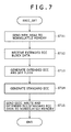
- FIG. 7 is a flowchart explanatory of how the memory controller 200 of the first embodiment operates upon receipt of an extended ECC set command EECC_SET.
- the host device 100 sets an extended ECC illustratively for the data to be stored for a prolonged period of time in the nonvolatile memory 300 so as to improve data retention characteristics.
- the host device 100 selects from the data in the nonvolatile memory 300 the extended ECC block 230 for which the extended ECC is to be set, and sends the starting address of the selected extended ECC block 230 to the memory controller 200 as the argument of the extended ECC set command EECC_SET.
- the memory controller 200 receives the extended ECC set command EECC_SET through the host interface section 201 and notifies the control unit 205 in the nonvolatile memory control section 202 thereof.
- the control unit 205 decodes the received command and determines that the command EECC_SET has been received. Using the command MEM_READ, the control unit 205 reads successively the data 210 of the extended ECC block 230 to be protected by the extended ECC along with the standard ECCs 215 from the nonvolatile memory 300 into the data buffer section 203 (in step ST 11 ). In this case, an error detection and correction process based on the standard ECC is carried out (in step ST 12 ).
- the standard/extended ECC processing unit 206 From the data in the data buffer section 203 , the standard/extended ECC processing unit 206 generates an extended ECC 220 .
- the control unit 205 sets the extended ECC validity flag FLEEV 402 to the extended ECC 220 (in step ST 13 ).
- the standard/extended ECC processing unit 206 generates a standard ECC 225 with regard to the extended ECC 220 (in step ST 14 ).
- the control unit 205 outputs the extended ECC write command EECC_WRITE, extended ECC 220 , and standard ECC 225 to the nonvolatile memory 300 through the memory interface section 204 (in step ST 15 ).
- FIG. 8 is a flowchart explanatory of how the memory controller 200 of the first embodiment operates upon receipt of a write command SYS_WRITE with its option OPT_ESET put in effect to set the extended ECC simultaneously.
- the host device 100 sends to the memory controller 200 the data write command SYS_WRITE with its option OPT_ESET set along with write data.
- the host interface section 201 receives the command SYS_WRITE and the write data into the data buffer section 203 and notifies the control unit 205 in the nonvolatile memory control section 202 thereof.
- the control unit 205 determines that the command SYS_WRITE has been received (in step ST 21 ).
- the standard/extended ECC processing unit 206 generates a standard ECC to be added per access unit while generating an extended ECC in parallel (in step ST 22 ).
- the control unit 205 outputs to the nonvolatile memory 300 the write command MEM_WRITE as well as the data 210 and standard ECC 215 held in the data buffer section 203 (in step ST 23
- the control unit 205 After performing the above process up to page n ⁇ 2 of the extended ECC block 230 (in step ST 24 ), the control unit 205 sets the flag FLEEV 402 to the generated extended ECC 220 (in step ST 25 ).
- the standard/extended ECC processing unit 206 further generates a standard ECC 225 with regard to the extended ECC 225 (in step ST 26 ).
- the control unit 205 then outputs the write command EECC_WRITE as well as the extended ECC 220 and standard ECC 225 held in the data buffer section 203 (in step ST 27 to the nonvolatile memory 300 through the memory interface section 204 .
- FIG. 9 is a schematic view showing a typical format of the extended ECC to be stored in the extended ECC area.
- the extended ECC 400 in FIG. 9 is made up of three fields: a physical address field 401 indicating the extended ECC block 230 to be protected by the extended ECC, an extended ECC validity flag field FLEEV 402 , and an extended ECC field 403 .
- FIG. 10 is a flowchart explanatory of how the memory controller 200 of the first embodiment operates upon receipt of a read command SYS_READ.
- the host device 100 sends the data read command SYS_READ to the memory controller 200 .
- the host interface section 201 of the memory controller 200 notifies the control unit 205 in the nonvolatile memory control section 202 thereof.
- the control unit 205 decodes the received command, determines that the read command SYS_READ has been received, and sends a read command MEM_READ to the nonvolatile memory 300 through the memory interface section 204 (in step ST 31 ).
- the control unit 205 sends data 210 and a standard ECC 215 to the data buffer section 203 through the memory interface section 204 .
- the standard/extended ECC processing unit 206 performs an error detection process using the standard ECC to correct any error of the data in the data buffer section 203 (in step ST 33 ).
- step ST 33 If no error is detected in step ST 33 or if the error detected in step ST 33 is found correctable using the standard ECC, then the control unit 205 sends the data 210 held in the data buffer section 203 to the host device through the host interface section 201 (in step ST 34 ).
- step ST 33 If in step ST 33 the detected error is found uncorrectable using the standard ECC, then the control unit 205 checks the value of the extended ECC validity flag FLEEV 402 (in step ST 35 ). If in step ST 35 the flag FLEEV 403 is found to have been cleared, that means the extended ECC is not set. In that case, the control unit 205 performs error handling before terminating the process (in step ST 42 ).
- step ST 35 the flag FLEEV 402 is found to be set, then the control unit 205 using the command MEM_READ receives all pages of the extended ECC block 230 from the nonvolatile memory 300 into the data buffer section 203 (in step ST 36 ). In this case, an error correction process is carried out using the standard ECC, and any error uncorrectable by the standard ECC is received uncorrected into the data buffer section 203 (in step ST 37 ).
- the control unit 205 reads the extended ECC 220 and standard ECC 225 using the command EECC_READ (in step ST 38 ).
- the standard/extended ECC processing unit 206 performs an extended ECC error correction process using the standard ECC 225 (in step ST 39 ), and carries out a data error detection and correction process on the data buffer section 203 using the extended ECC 220 (in step ST 40 ). In this step, the data uncorrectable by the standard ECC is corrected using the extended ECC.
- step ST 41 If in step ST 41 no error is found to be uncorrectable by the extended ECC, the control unit 205 sends the corrected data held in the data buffer section 203 to the host device 100 through the host interface section 201 (in step ST 34 ). If in step ST 42 any error is found to be uncorrectable even by the extended ECC, then the control unit 205 performs error handling (in step ST 42 ) and terminates the process.
- the control unit 205 determines whether a corrected data write-back option OWET 3 is set in the read command SYS_READ coming from the host device 100 (in step ST 43 ). If the option is found to be set, the control unit 205 writes the corrected data held in the data buffer section 203 back to the nonvolatile memory 300 using the commands MEM_WRITE and EECC_WRITE (in step ST 44 ).
- FIG. 11 is a schematic view explanatory of how the product code is used as the extended ECC for error detection and correction
- FIG. 12 is a schematic view explanatory of how multiple error correction codes are used as the extended ECC for error detection and correction.
- Using the product code as the extended ECC involves calculating an ECC in each of the row and column directions of a block of data arrayed in the two directions and repeating corrections in the row and column directions to correct errors in each direction.
- FIG. 11 shows an example in which one error can be corrected in each of the rows and columns.
- the ECCs in the row direction are stored in the standard ECC area, and the ECCs in the column direction are held in the extended ECC area.
- the extended ECC is the combination of a row-direction ECC with a column-direction ECC and the value of the row-direction ECC coincides with that of the standard ECC, so that the extended ECC need not be stored in the extended ECC area.
- the product code-based error correction scheme is characterized in that even if error correction is unavailable in the initial status (i.e., status STS 0 ), corrections are repeated in the row and column directions so as to correct all errors.
- the row-direction ECC and column-direction. ECC are processed using the standard ECC and extended ECC, respectively.
- the error correction capability is reinforced even if the same error correction scheme is utilized in the row and column directions. This provides the advantage of a single circuit generating standard and extended ECCs and carrying out the error correction process as well.
- FIG. 12 is an example in which the Hamming code capable of single-error correction is used as the standard ECC while the BCH code capable of quadruple-error correction is used as the extended ECC.
- the data to be protected by the extended ECC has three errors. Since the extended ECC is capable of quadruple-error correction, these three errors can be corrected using the extended ECC (status STS 12 ).
- the extended ECC 220 is attached to each of the extended ECC blocks 230 . This arrangement permits correction of the errors that cannot be corrected using the standard ECC 215 only.
- FIG. 13 is a flowchart explanatory of how the memory controller 200 of the first embodiment operates upon receipt of an extended ECC clear command EECC_CLR.
- the host device 100 sends the extended ECC clear command EECC_CLR to the memory controller 200 .
- the host interface section 201 of the memory controller 200 notifies the control unit 205 in the nonvolatile memory control section 202 thereof.
- the control unit 205 decodes the received command and determines that the extended ECC clear command EECC_CLR has been received.
- the control unit 205 prepares the data from which the extended ECC validity flag FLEEV 402 has been cleared (in step ST 51 ).
- the control unit 205 sends the extended ECC write command EECC_WRITE to the nonvolatile memory 300 through the memory interface 204 , thereby clearing the designated extended ECC in the extended ECC block of the extended ECC area 305 (in step ST 52 ).
- FIG. 14 is a schematic view showing a configuration example of a memory system 10 A which constitutes the second embodiment of the present invention and which includes a nonvolatile memory apparatus according to the invention.
- the memory system 10 A of the second embodiment differs from the memory system 10 of the first embodiment in the following aspects:
- the memory controller 200 processes both standard and extended ECCs.
- the standard ECCs are processed by a nonvolatile memory 300 A.
- a nonvolatile memory control section 202 A of a memory controller 200 A in the memory system 10 A includes an extended ECC processing unit 207 replacing the standard/extended ECC processing unit of the first embodiment.
- the nonvolatile memory 300 A contains a data buffer section 307 and a standard ECC processing section 308 , both controlled by the control section 306 .
- the host device 100 of the second embodiment issues the commands SYS_WRITE, SYS_READ, EECC_SET, EECC_GET, and EECC_CLR to the memory controller.
- the nonvolatile memory 300 A includes three functions: the function of generating standard ECCs, the function of performing error detection and correction using the standard ECCs, and the function of notifying the memory controller 200 A of any error uncorrectable by the standard ECC.
- the memory controller 200 A issues the commands MEM_WRITE, MEM_READ, EECC_READ, and EECC_WRITE to the nonvolatile memory 300 A but does not add the standard ECC to data upon data transfer thereto unlike in the first embodiment. More specifically, upon a data write using the command MEM_WRITE, the memory controller 200 A does not include the standard ECC into the received data. It is the nonvolatile memory 300 A that internally adds the standard ECC to the data for storage therein. Upon a data read using the command MEM_READ, the nonvolatile memory 200 A sends the data corrected by the standard ECC to the memory controller 200 A.
- the nonvolatile memory 300 A When an extended ECC is to be stored using the command EECC_WRITE, no standard ECC is included in the received extended ECC information.
- the nonvolatile memory 300 A internally adds the standard ECC to the extended ECC information for storage therein.
- the nonvolatile memory 300 A sends the extended ECC corrected by the standard ECC to the memory controller 200 A.
- the nonvolatile memory 300 A When data is to be written to the nonvolatile memory 300 A using the command MEM_READ, the nonvolatile memory 300 A receives the command through the memory interface section 301 , notifies the control section 306 thereof, and receives the write data into the data buffer section 307 .
- the control section 306 decodes the command, determines the command to be MEM_WRITE, creates a standard ECC from the write data held in the data buffer section 307 , writes the data to the data area 303 , and writes the standard ECC to the standard ECC area 304 .
- the nonvolatile memory 300 A When data is to be read from the nonvolatile memory 300 A using the command MEM_READ, the nonvolatile memory 300 A receives the command through the memory interface section 301 and notifies the control section 306 thereof.
- the control section 306 decodes the command, determines the command to be MEM_READ, reads the data from the data area 303 and standard ECC area 304 into the data buffer section 307 , causes the standard ECC processing section to perform error detection and correction of the data, and sends the data to the memory controller 200 A through the memory interface section 301 . If any uncorrectable error is detected, the control section 306 notifies the memory controller 200 A thereof and sends the uncorrected data to the memory controller 200 A through the memory interface section 301 .
- FIG. 15 is a flowchart explanatory of how the memory controller 200 A of the second embodiment operates upon receipt of the command SYS_READ. What takes place in steps ST 32 A, ST 33 A, ST 37 A, and ST 39 A is different from the comparable processing by the first embodiment of which the flowchart is shown in FIG. 10 . The other steps are the same as those of the first embodiment.
- the data corrected by the standard ECC is received in steps ST 32 A, ST 37 A, and ST 39 A.
- the memory controller 200 A receives from the nonvolatile memory 300 A information indicating whether there has occurred an error uncorrectable by the standard ECC, and determines whether or not to perform an extended ECC process. If the data is found to have developed an uncorrectable error in the standard ECC processing section inside the nonvolatile memory 300 A, then the uncorrected data is output to the memory controller 200 A.
- FIG. 16 is a schematic view showing a configuration example of a memory system 10 B which constitutes the third embodiment of the present invention and which includes a nonvolatile memory apparatus according to the invention.
- the memory system 10 B of the third embodiment differs from the memory system 10 of the first embodiment in the following aspects:
- the memory controller 200 processes standard and extended ECCs.
- the standard ECCs are processed by a memory controller 200 B and the extended ECCs by a host device 100 B.
- a nonvolatile memory control section 202 B of the memory controller 200 B in the memory system 10 B contains a standard ECC processing unit 208 replacing the standard/extended ECC processing unit.
- the host device 100 B includes an extended ECC processing section 103 that is controlled by the CPU 101 .
- the extended ECC processing section 103 of the host device 100 B may be implemented using either hardware or software.
- the host device 100 B includes the function of generating an extended ECC and the function of performing error detection and correction using the extended ECC.
- the host device 100 B issues the commands SYS_WRITE, SYS_READ, EECC_SET, EECC_GET, and EECC_CLR to the memory controller 200 B. Unlike in the first embodiment, the host device 100 B issues these commands not only for data access but also for extended ECC processing.
- the write operation by use of the command SYS_WRITE is the same as with the first embodiment.
- the memory controller 200 B has the function of giving notification that an error uncorrectable by the standard ECC has occurred, unlike in the first embodiment.
- the host device 100 B reads the page data 210 of the extended ECC block 230 using the command SYS_READ and performs error correction using the extended ECC.
- the extended ECC is set using the command EECC_SET. Unlike in the first embodiment, the host device 100 B sends the command EECC_SET along with an extended ECC in the format shown in FIG. 9 to the memory controller 200 B.
- the extended ECC is read using the command EECC_GET in the same manner as with the first embodiment.
- the extended ECC is cleared using the command EECC_CLR also in the same manner as with the first embodiment.
- the memory controller 200 B issues the commands MEM_WRITE, MEM_READ, EECC_WRITE, and EECC_READ to the nonvolatile memory 300 in the same manner as with the first embodiment.
- FIGS. 17A and 17B are flowcharts explanatory of how the host device 100 B and memory controller 200 B operate as part of the third embodiment upon processing of the command EECC_SET.
- FIG. 17A shows how the host device 100 B works and
- FIG. 17B indicates how the memory controller 200 B operates.
- the host device 100 B sends the command SYS_READ to the memory controller 200 B so as to read the page data 210 of the extended ECC block 230 to be protected by an extended ECC (in step ST 61 ).
- the host device 100 B generates an extended ECC from the read data and sets an extended ECC validity flag FLEEV 402 (in step ST 62 .
- the host device 100 B then sends the generated extended ECC together with the command EECC_SET to the memory controller 200 B (in step ST 63 ).
- the host interface section 201 in the memory controller 200 B receives the command EECC_SET, notifies the control unit 205 in the nonvolatile memory control section 202 B thereof, and writes the extended ECC 403 and extended ECC validity flag FLEEV 402 to the data buffer section 203 .
- the control unit 205 decodes the received command and determines that the command EECC_SET has been received. The control unit 205 then arranges the received extended ECC 403 and flag FLEEV 402 into the format shown in FIG. 9 (in step ST 71 ), calculates the standard ECC, and sends the ECC along with the command EECC_WRITE to the nonvolatile memory 300 (in step ST 72 ).
- FIG. 18 is a flowchart explanatory of how the host device 100 B operates upon reading data.
- the host device 100 B reads data using the command SYS_READ. Upon receipt of notification that that an error uncorrectable by the standard ECC has occurred from the memory controller 200 B in step ST 33 B, the host device 100 B attempts to correct the error using the extended ECC (in steps ST 36 B through ST 40 B).
- the host device 100 B reads the page data 210 of the extended ECC block 230 using the command SYS_READ (in step ST 36 B). By this time, the received data 210 has been corrected using the standard ECC 215 . If there is found an error uncorrectable by the standard ECC 215 , the host device 100 B receives the uncorrected data 210 (in step ST 37 B). The host device 100 B then sends to the memory controller 200 B the command EECC_GET by which to read the extended ECC 220 (in step ST 38 B), and receives the extended ECC 220 that has been corrected using the standard ECC (in step ST 39 B). Thereafter, steps ST 40 and ST 41 are the same as those of the first embodiment except that the processing is performed by the host device 100 B.
- FIG. 19 is a schematic view showing a configuration example of a memory system 100 which constitutes the fourth embodiment of the present invention and which includes a nonvolatile memory apparatus according to the invention.
- the memory system 100 of the fourth embodiment differs from the memory system 10 of the first embodiment in the following aspects:
- the memory controller 200 processes both standard and extended ECCs.
- the standard and extended ECCs are processed by a nonvolatile memory 300 C.
- a nonvolatile memory control section 202 C of a memory controller 200 C in the memory system 100 does not include the standard/extended ECC processing unit.
- the nonvolatile memory 300 C contains the data buffer section 307 and standard/extended ECC processing section 309 .
- the standard and extended ECCs are processed by the nonvolatile memory 300 C; the processes carried out by the memory controller 200 in the first embodiment are taken over by the nonvolatile memory 300 C in the fourth embodiment.
- FIG. 20 is a schematic view showing a configuration example of a memory system 10 D which constitutes the fifth embodiment of the present invention and which includes a nonvolatile memory apparatus according to the invention.
- the memory system 10 D of the fifth embodiment differs from the memory system 10 of the first embodiment in the following aspects:
- the memory controller 200 processes both standard and extended ECCs.
- the standard ECCs are processed by a nonvolatile memory 300 D and the extended ECCs by a host device 100 D.
- a nonvolatile memory control section 202 D of a memory controller 200 D in the memory system 10 D does not include the standard/extended ECC processing section.
- the nonvolatile memory 300 D contains the data buffer section 307 and standard ECC processing section 308 , and the host device 100 D includes the extended ECC processing section 103 .
- the standard ECCs are processed by the nonvolatile memory 300 D and the extended ECCs are handled by the host device 100 D.
- the standard ECCs are processed in the same manner as with the second embodiment.
- the memory controller 200 D does not have the function of processing extended ECCs. Instead, the memory controller 200 D includes the function of notifying the host device 100 D of any error which is uncorrectable by the standard ECC and which is output from the nonvolatile memory 300 D.
- the extended ECCs are processed in the same manner as with the third embodiment.
- FIG. 21 is a schematic view showing a configuration example of a memory system 10 E which constitutes the sixth embodiment of the present invention and which includes a nonvolatile memory apparatus according to the invention.
- the memory system 10 E of the sixth embodiment differs from the memory system 10 of the first embodiment in the following aspects:
- the memory controller 200 processes both standard and extended ECCs.
- the standard and extended ECCs are processed by a host device 100 E.
- a nonvolatile memory control section 202 E of a memory controller 200 E in the memory system 10 E does not include the standard/extended ECC processing section.
- the host device 100 E includes the extended ECC processing section 103 and a standard ECC processing section 104 . Because the extended ECC processing section of the host device 100 E needs to perform its processing when the standard ECC processing section has developed an uncorrectable error, this extended ECC processing section may be implemented by software.
- the standard and extended ECCs are processed by the host device 100 E; the processes carried out by the memory controller 200 in the first embodiment are taken over by the host device 100 E in the sixth embodiment.
- FIG. 22 is a schematic view showing a configuration example of a memory system 10 F which constitutes the seventh embodiment of the present invention and which includes a nonvolatile memory apparatus according to the invention.
- the memory system 10 F of the seventh embodiment differs from the memory system 10 of the first embodiment in the following aspects:
- the host device 100 and the memory controller 200 are structured separately.
- a memory controller 200 F is structured to be included in a host device 100 F.
- the memory system 10 F of the seventh embodiment has no need for the host interface section 102 or 201 .
- the other components and their functions of the seventh embodiment are the same as those of the first embodiment.
Applications Claiming Priority (4)
| Application Number | Priority Date | Filing Date | Title |
|---|---|---|---|
| JP2009210433 | 2009-09-11 | ||
| JPP2009-210433 | 2009-09-11 | ||
| JP2010171690A JP5540969B2 (ja) | 2009-09-11 | 2010-07-30 | 不揮発性メモリ装置、メモリコントローラ、およびメモリシステム |
| JPP2010-171690 | 2010-07-30 |
Related Child Applications (1)
| Application Number | Title | Priority Date | Filing Date |
|---|---|---|---|
| US13/110,215 Continuation-In-Part US8382524B2 (en) | 2010-05-21 | 2011-05-18 | Electrical connector having thick film layers |
Publications (2)
| Publication Number | Publication Date |
|---|---|
| US20110066923A1 US20110066923A1 (en) | 2011-03-17 |
| US8438457B2 true US8438457B2 (en) | 2013-05-07 |
Family
ID=43731671
Family Applications (1)
| Application Number | Title | Priority Date | Filing Date |
|---|---|---|---|
| US12/874,914 Active 2031-07-28 US8438457B2 (en) | 2009-09-11 | 2010-09-02 | Nonvolatile memory apparatus, memory controller, and memory system |
Country Status (3)
| Country | Link |
|---|---|
| US (1) | US8438457B2 (zh) |
| JP (1) | JP5540969B2 (zh) |
| CN (1) | CN102023901B (zh) |
Cited By (5)
| Publication number | Priority date | Publication date | Assignee | Title |
|---|---|---|---|---|
| US20160342473A1 (en) * | 2015-05-20 | 2016-11-24 | International Business Machines Corporation | Extended error correction coding data storage |
| US9772900B2 (en) | 2014-07-10 | 2017-09-26 | Samsung Electronics Co., Ltd. | Tiered ECC single-chip and double-chip Chipkill scheme |
| US10289475B2 (en) | 2015-01-21 | 2019-05-14 | Toshiba Memory Corporation | Memory system |
| US10776019B2 (en) | 2017-09-20 | 2020-09-15 | Toshiba Memory Corporation | Memory system and method of controlling nonvolatile memory |
| US11099927B2 (en) | 2015-01-21 | 2021-08-24 | Toshiba Memory Corporation | Memory system |
Families Citing this family (22)
| Publication number | Priority date | Publication date | Assignee | Title |
|---|---|---|---|---|
| KR101803970B1 (ko) * | 2011-03-16 | 2017-12-28 | 삼성전자주식회사 | 컨텐트를 구성하는 장치 및 방법 |
| KR101843918B1 (ko) | 2011-04-25 | 2018-04-02 | 삼성전자주식회사 | 메모리 컨트롤러, 이를 포함하는 메모리 시스템 및 그 동작 방법 |
| JP2012252558A (ja) * | 2011-06-03 | 2012-12-20 | Sony Corp | 不揮発性メモリ、メモリコントローラ、不揮発性メモリのアクセス方法、およびプログラム |
| JP5845876B2 (ja) * | 2011-12-20 | 2016-01-20 | ソニー株式会社 | 記憶制御装置、記憶装置、情報処理システム、および、それらにおける処理方法 |
| US8898541B2 (en) * | 2011-11-30 | 2014-11-25 | Sony Corporation | Storage controller, storage device, information processing system, and storage controlling method |
| KR101889362B1 (ko) * | 2012-02-06 | 2018-09-20 | 에스케이하이닉스 주식회사 | 비휘발성 메모리 장치 및 그 동작 방법, 이를 이용하는 데이터 처리 시스템 |
| US8954825B2 (en) | 2012-03-06 | 2015-02-10 | Micron Technology, Inc. | Apparatuses and methods including error correction code organization |
| JP2014086062A (ja) * | 2012-10-29 | 2014-05-12 | Sony Corp | 記憶制御装置、記憶装置、情報処理システム、および、記憶制御方法 |
| US9146809B2 (en) * | 2013-10-07 | 2015-09-29 | Macronix International Co., Ltd. | ECC method for double pattern flash memory |
| JP6028709B2 (ja) | 2013-10-18 | 2016-11-16 | ソニー株式会社 | 記憶制御装置、記憶装置、情報処理システムおよびその記憶制御方法 |
| CN104637542B (zh) * | 2013-11-11 | 2018-03-13 | 旺宏电子股份有限公司 | 储存对应于数据的错误更正码的存储器装置及其操作方法 |
| US9535785B2 (en) | 2014-01-17 | 2017-01-03 | Macronix International Co., Ltd. | ECC method for flash memory |
| US9542268B2 (en) * | 2014-01-29 | 2017-01-10 | Macronix International Co., Ltd. | Dynamic data density ECC |
| US9520901B2 (en) | 2014-03-06 | 2016-12-13 | Kabushiki Kaisha Toshiba | Memory controller, memory system, and memory control method |
| JP2016062463A (ja) * | 2014-09-19 | 2016-04-25 | 株式会社東芝 | メモリシステム、誤り訂正装置、および誤り訂正方法 |
| US9558066B2 (en) * | 2014-09-26 | 2017-01-31 | Intel Corporation | Exchanging ECC metadata between memory and host system |
| US9845268B2 (en) * | 2016-05-23 | 2017-12-19 | Kennametal Inc. | Sintered ceramic bodies and applications thereof |
| US10290353B2 (en) * | 2016-09-06 | 2019-05-14 | Western Digital Technologies, Inc. | Error mitigation for 3D NAND flash memory |
| JP6957392B2 (ja) | 2018-03-15 | 2021-11-02 | キオクシア株式会社 | メモリシステム |
| KR102611860B1 (ko) * | 2018-11-05 | 2023-12-11 | 에스케이하이닉스 주식회사 | 디코딩 회로 및 이를 포함하는 반도체 메모리 장치 |
| KR20200078830A (ko) * | 2018-12-24 | 2020-07-02 | 에스케이하이닉스 주식회사 | 메모리 시스템 및 메모리 모듈 |
| US11514174B2 (en) * | 2019-01-23 | 2022-11-29 | Micron Technology, Inc. | Memory devices with cryptographic components |
Citations (9)
| Publication number | Priority date | Publication date | Assignee | Title |
|---|---|---|---|---|
| JPH08166910A (ja) | 1994-12-15 | 1996-06-25 | Nec Corp | データ修復方法 |
| JPH09167120A (ja) | 1995-12-15 | 1997-06-24 | Denso Corp | 記憶装置の誤り訂正装置 |
| JP2001117825A (ja) | 1999-10-20 | 2001-04-27 | Sharp Corp | データ記録装置およびデータ再生装置 |
| JP2004348824A (ja) | 2003-05-21 | 2004-12-09 | Toshiba Corp | Eccエンコード方法、eccエンコード装置 |
| US20060256615A1 (en) | 2005-05-10 | 2006-11-16 | Larson Thane M | Horizontal and vertical error correction coding (ECC) system and method |
| US20080126905A1 (en) | 2006-11-29 | 2008-05-29 | Matsushita Electric Industrial Co., Ltd. | Memory control device, computer system and data reproducing and recording device |
| JP2008192054A (ja) | 2007-02-07 | 2008-08-21 | Megachips Lsi Solutions Inc | 半導体メモリシステム |
| US20110041037A1 (en) * | 2009-08-11 | 2011-02-17 | Texas Memory Systems, Inc. | FLASH-based Memory System with Static or Variable Length Page Stripes including Data Protection Information and Auxiliary Protection Stripes |
| US20120155174A1 (en) * | 2006-05-15 | 2012-06-21 | Apple Inc. | Use of Alternative Value in Cell Detection |
Family Cites Families (5)
| Publication number | Priority date | Publication date | Assignee | Title |
|---|---|---|---|---|
| JP2003196142A (ja) * | 2001-12-25 | 2003-07-11 | Sony Corp | ライトワンス型メモリ装置及びファイル管理方法 |
| JP4586469B2 (ja) * | 2004-09-15 | 2010-11-24 | ソニー株式会社 | メモリ制御装置、メモリ制御方法、プログラム |
| JP2006195569A (ja) * | 2005-01-11 | 2006-07-27 | Sony Corp | 記憶装置 |
| JP4564520B2 (ja) * | 2007-08-31 | 2010-10-20 | 株式会社東芝 | 半導体記憶装置およびその制御方法 |
| JP4538034B2 (ja) * | 2007-09-26 | 2010-09-08 | 株式会社東芝 | 半導体記憶装置、及びその制御方法 |
-
2010
- 2010-07-30 JP JP2010171690A patent/JP5540969B2/ja not_active Expired - Fee Related
- 2010-09-02 US US12/874,914 patent/US8438457B2/en active Active
- 2010-09-06 CN CN201010275225XA patent/CN102023901B/zh not_active Expired - Fee Related
Patent Citations (12)
| Publication number | Priority date | Publication date | Assignee | Title |
|---|---|---|---|---|
| JPH08166910A (ja) | 1994-12-15 | 1996-06-25 | Nec Corp | データ修復方法 |
| JPH09167120A (ja) | 1995-12-15 | 1997-06-24 | Denso Corp | 記憶装置の誤り訂正装置 |
| JP2001117825A (ja) | 1999-10-20 | 2001-04-27 | Sharp Corp | データ記録装置およびデータ再生装置 |
| JP2004348824A (ja) | 2003-05-21 | 2004-12-09 | Toshiba Corp | Eccエンコード方法、eccエンコード装置 |
| US20060256615A1 (en) | 2005-05-10 | 2006-11-16 | Larson Thane M | Horizontal and vertical error correction coding (ECC) system and method |
| JP2006318461A (ja) | 2005-05-10 | 2006-11-24 | Hewlett-Packard Development Co Lp | 水平及び垂直のエラー訂正符号化(ecc)システム及び方法 |
| US20120155174A1 (en) * | 2006-05-15 | 2012-06-21 | Apple Inc. | Use of Alternative Value in Cell Detection |
| US20080126905A1 (en) | 2006-11-29 | 2008-05-29 | Matsushita Electric Industrial Co., Ltd. | Memory control device, computer system and data reproducing and recording device |
| JP2008139908A (ja) | 2006-11-29 | 2008-06-19 | Matsushita Electric Ind Co Ltd | メモリ制御装置、コンピュータシステム及びデータ再生記録装置 |
| JP2008192054A (ja) | 2007-02-07 | 2008-08-21 | Megachips Lsi Solutions Inc | 半導体メモリシステム |
| US20110041037A1 (en) * | 2009-08-11 | 2011-02-17 | Texas Memory Systems, Inc. | FLASH-based Memory System with Static or Variable Length Page Stripes including Data Protection Information and Auxiliary Protection Stripes |
| US20110213919A1 (en) * | 2009-08-11 | 2011-09-01 | Texas Memory Systems, Inc. | FLASH-based Memory System with Static or Variable Length Page Stripes Including Data Protection Information and Auxiliary Protection Stripes |
Non-Patent Citations (1)
| Title |
|---|
| U.S. Appl. No. 12/816,685, filed Jun. 16, 2010, Nakanishi, et al. |
Cited By (9)
| Publication number | Priority date | Publication date | Assignee | Title |
|---|---|---|---|---|
| US9772900B2 (en) | 2014-07-10 | 2017-09-26 | Samsung Electronics Co., Ltd. | Tiered ECC single-chip and double-chip Chipkill scheme |
| US10289475B2 (en) | 2015-01-21 | 2019-05-14 | Toshiba Memory Corporation | Memory system |
| US11099927B2 (en) | 2015-01-21 | 2021-08-24 | Toshiba Memory Corporation | Memory system |
| US11960355B2 (en) | 2015-01-21 | 2024-04-16 | Kioxia Corporation | Memory system |
| US20160342473A1 (en) * | 2015-05-20 | 2016-11-24 | International Business Machines Corporation | Extended error correction coding data storage |
| US20160342469A1 (en) * | 2015-05-20 | 2016-11-24 | International Business Machines Corporation | Extended error correction coding data storage |
| US10027349B2 (en) * | 2015-05-20 | 2018-07-17 | International Business Machines Corporation | Extended error correction coding data storage |
| US10063263B2 (en) * | 2015-05-20 | 2018-08-28 | International Business Machines Corporation | Extended error correction coding data storage |
| US10776019B2 (en) | 2017-09-20 | 2020-09-15 | Toshiba Memory Corporation | Memory system and method of controlling nonvolatile memory |
Also Published As
| Publication number | Publication date |
|---|---|
| US20110066923A1 (en) | 2011-03-17 |
| CN102023901A (zh) | 2011-04-20 |
| JP5540969B2 (ja) | 2014-07-02 |
| JP2011081776A (ja) | 2011-04-21 |
| CN102023901B (zh) | 2013-06-05 |
Similar Documents
| Publication | Publication Date | Title |
|---|---|---|
| US8438457B2 (en) | Nonvolatile memory apparatus, memory controller, and memory system | |
| US10847246B2 (en) | Memory systems performing reconfigurable error correction operation using ECC engine with fixed error correction capability | |
| US7899980B2 (en) | Flash memory system and data writing method thereof | |
| KR101659888B1 (ko) | 플래시 메모리 제어 방법, 제어기 및 전자 장치 | |
| US7581153B2 (en) | Memory with embedded error correction codes | |
| JP5529751B2 (ja) | メモリアレイにおけるエラー訂正 | |
| JP2015018451A (ja) | メモリコントローラ、記憶装置およびメモリ制御方法 | |
| US20200142771A1 (en) | Error correction code decoders, semiconductor memory devices and memory systems | |
| US9003153B2 (en) | Method of storing blocks of data in a plurality of memory devices in a redundant manner, a memory controller and a memory system | |
| US20130117632A1 (en) | Storage control apparatus | |
| US11218165B2 (en) | Memory-mapped two-dimensional error correction code for multi-bit error tolerance in DRAM | |
| US11030040B2 (en) | Memory device detecting an error in write data during a write operation, memory system including the same, and operating method of memory system | |
| US20220180961A1 (en) | Memory device and read method thereof | |
| JP2010079856A (ja) | 記憶装置およびメモリ制御方法 | |
| US10756764B2 (en) | Memory system and control method | |
| US10665297B2 (en) | Memory systems for memory devices and methods of operating the memory systems | |
| US20190354435A1 (en) | Memory system and operating method thereof | |
| US10922025B2 (en) | Nonvolatile memory bad row management | |
| JP6479638B2 (ja) | ビデオサーバ装置およびデータ書き込み/読み出し方法 | |
| CN110058955B (zh) | 具有错误纠正功能的内存和相关内存系统 | |
| JP2012003569A (ja) | メモリコントローラ及びメモリコントローラを備えるフラッシュメモリシステム、並びにフラッシュメモリの制御方法 | |
| US11775205B2 (en) | Semiconductor storage device and reading method | |
| US11360853B2 (en) | Access method | |
| US20230385147A1 (en) | Memory control circuit, memory, and memory module | |
| JP2018055400A (ja) | メモリコントローラ、メモリシステム及びメモリ制御方法 |
Legal Events
| Date | Code | Title | Description |
|---|---|---|---|
| AS | Assignment |
Owner name: SONY CORPORATION, JAPAN Free format text: ASSIGNMENT OF ASSIGNORS INTEREST;ASSIGNORS:KOSHIYAMA, JUNICHI;NAKANISHI, KENICHI;TSUTSUI, KEIICHI;REEL/FRAME:025327/0564 Effective date: 20100924 |
|
| FEPP | Fee payment procedure |
Free format text: PAYOR NUMBER ASSIGNED (ORIGINAL EVENT CODE: ASPN); ENTITY STATUS OF PATENT OWNER: LARGE ENTITY |
|
| STCF | Information on status: patent grant |
Free format text: PATENTED CASE |
|
| FPAY | Fee payment |
Year of fee payment: 4 |
|
| MAFP | Maintenance fee payment |
Free format text: PAYMENT OF MAINTENANCE FEE, 8TH YEAR, LARGE ENTITY (ORIGINAL EVENT CODE: M1552); ENTITY STATUS OF PATENT OWNER: LARGE ENTITY Year of fee payment: 8 |