US8331079B2 - Multilayer ceramic capacitor and method of manufacturing the same - Google Patents
Multilayer ceramic capacitor and method of manufacturing the same Download PDFInfo
- Publication number
- US8331079B2 US8331079B2 US12/941,589 US94158910A US8331079B2 US 8331079 B2 US8331079 B2 US 8331079B2 US 94158910 A US94158910 A US 94158910A US 8331079 B2 US8331079 B2 US 8331079B2
- Authority
- US
- United States
- Prior art keywords
- inner electrodes
- lamination
- multilayer ceramic
- ceramic capacitor
- passivation layer
- Prior art date
- Legal status (The legal status is an assumption and is not a legal conclusion. Google has not performed a legal analysis and makes no representation as to the accuracy of the status listed.)
- Active, expires
Links
- 239000003985 ceramic capacitor Substances 0.000 title claims abstract description 33
- 238000004519 manufacturing process Methods 0.000 title claims abstract description 10
- 238000002161 passivation Methods 0.000 claims abstract description 41
- 238000003475 lamination Methods 0.000 claims abstract description 27
- 229910019092 Mg-O Inorganic materials 0.000 claims abstract description 16
- 229910019395 Mg—O Inorganic materials 0.000 claims abstract description 16
- 238000010304 firing Methods 0.000 claims description 10
- QVGXLLKOCUKJST-UHFFFAOYSA-N atomic oxygen Chemical compound [O] QVGXLLKOCUKJST-UHFFFAOYSA-N 0.000 claims description 9
- 238000000034 method Methods 0.000 claims description 9
- 229910052760 oxygen Inorganic materials 0.000 claims description 9
- 239000001301 oxygen Substances 0.000 claims description 9
- 239000011521 glass Substances 0.000 claims description 8
- 239000000919 ceramic Substances 0.000 description 38
- 239000011230 binding agent Substances 0.000 description 6
- 229910000990 Ni alloy Inorganic materials 0.000 description 4
- 229910002113 barium titanate Inorganic materials 0.000 description 4
- 239000003960 organic solvent Substances 0.000 description 4
- 230000003647 oxidation Effects 0.000 description 4
- 238000007254 oxidation reaction Methods 0.000 description 4
- 239000002002 slurry Substances 0.000 description 4
- 229910010293 ceramic material Inorganic materials 0.000 description 3
- -1 for example Substances 0.000 description 3
- 229910052751 metal Inorganic materials 0.000 description 3
- 239000002184 metal Substances 0.000 description 3
- 239000000203 mixture Substances 0.000 description 3
- 239000000843 powder Substances 0.000 description 3
- 229920005989 resin Polymers 0.000 description 3
- 239000011347 resin Substances 0.000 description 3
- 238000004458 analytical method Methods 0.000 description 2
- JRPBQTZRNDNNOP-UHFFFAOYSA-N barium titanate Chemical compound [Ba+2].[Ba+2].[O-][Ti]([O-])([O-])[O-] JRPBQTZRNDNNOP-UHFFFAOYSA-N 0.000 description 2
- 230000005540 biological transmission Effects 0.000 description 2
- 239000003990 capacitor Substances 0.000 description 2
- 229910052804 chromium Inorganic materials 0.000 description 2
- 230000000052 comparative effect Effects 0.000 description 2
- DOIRQSBPFJWKBE-UHFFFAOYSA-N dibutyl phthalate Chemical compound CCCCOC(=O)C1=CC=CC=C1C(=O)OCCCC DOIRQSBPFJWKBE-UHFFFAOYSA-N 0.000 description 2
- 238000007606 doctor blade method Methods 0.000 description 2
- 229910052748 manganese Inorganic materials 0.000 description 2
- 229910052759 nickel Inorganic materials 0.000 description 2
- 230000035515 penetration Effects 0.000 description 2
- 239000002904 solvent Substances 0.000 description 2
- VEALVRVVWBQVSL-UHFFFAOYSA-N strontium titanate Chemical compound [Sr+2].[O-][Ti]([O-])=O VEALVRVVWBQVSL-UHFFFAOYSA-N 0.000 description 2
- OAYXUHPQHDHDDZ-UHFFFAOYSA-N 2-(2-butoxyethoxy)ethanol Chemical compound CCCCOCCOCCO OAYXUHPQHDHDDZ-UHFFFAOYSA-N 0.000 description 1
- VXQBJTKSVGFQOL-UHFFFAOYSA-N 2-(2-butoxyethoxy)ethyl acetate Chemical compound CCCCOCCOCCOC(C)=O VXQBJTKSVGFQOL-UHFFFAOYSA-N 0.000 description 1
- ZNQVEEAIQZEUHB-UHFFFAOYSA-N 2-ethoxyethanol Chemical compound CCOCCO ZNQVEEAIQZEUHB-UHFFFAOYSA-N 0.000 description 1
- KXGFMDJXCMQABM-UHFFFAOYSA-N 2-methoxy-6-methylphenol Chemical compound [CH]OC1=CC=CC([CH])=C1O KXGFMDJXCMQABM-UHFFFAOYSA-N 0.000 description 1
- RSWGJHLUYNHPMX-UHFFFAOYSA-N Abietic-Saeure Natural products C12CCC(C(C)C)=CC2=CCC2C1(C)CCCC2(C)C(O)=O RSWGJHLUYNHPMX-UHFFFAOYSA-N 0.000 description 1
- 101001091423 Agaricus bisporus Polyphenol oxidase 2 Proteins 0.000 description 1
- 101000611523 Arabidopsis thaliana Protoporphyrinogen oxidase 2, chloroplastic/mitochondrial Proteins 0.000 description 1
- RYGMFSIKBFXOCR-UHFFFAOYSA-N Copper Chemical compound [Cu] RYGMFSIKBFXOCR-UHFFFAOYSA-N 0.000 description 1
- 239000001293 FEMA 3089 Substances 0.000 description 1
- 229910018553 Ni—O Inorganic materials 0.000 description 1
- KHPCPRHQVVSZAH-HUOMCSJISA-N Rosin Natural products O(C/C=C/c1ccccc1)[C@H]1[C@H](O)[C@@H](O)[C@@H](O)[C@@H](CO)O1 KHPCPRHQVVSZAH-HUOMCSJISA-N 0.000 description 1
- 229910052784 alkaline earth metal Inorganic materials 0.000 description 1
- 150000001342 alkaline earth metals Chemical class 0.000 description 1
- 229920000180 alkyd Polymers 0.000 description 1
- 125000003118 aryl group Chemical group 0.000 description 1
- 230000015556 catabolic process Effects 0.000 description 1
- 239000001913 cellulose Substances 0.000 description 1
- 229920002678 cellulose Polymers 0.000 description 1
- 229910052802 copper Inorganic materials 0.000 description 1
- 239000010949 copper Substances 0.000 description 1
- 230000007547 defect Effects 0.000 description 1
- 238000006731 degradation reaction Methods 0.000 description 1
- 229960002380 dibutyl phthalate Drugs 0.000 description 1
- 239000003822 epoxy resin Substances 0.000 description 1
- 150000002148 esters Chemical class 0.000 description 1
- 238000007429 general method Methods 0.000 description 1
- 229910052749 magnesium Inorganic materials 0.000 description 1
- 239000001095 magnesium carbonate Substances 0.000 description 1
- ZLNQQNXFFQJAID-UHFFFAOYSA-L magnesium carbonate Chemical compound [Mg+2].[O-]C([O-])=O ZLNQQNXFFQJAID-UHFFFAOYSA-L 0.000 description 1
- 229910000021 magnesium carbonate Inorganic materials 0.000 description 1
- 238000010295 mobile communication Methods 0.000 description 1
- 238000012986 modification Methods 0.000 description 1
- 230000004048 modification Effects 0.000 description 1
- 229920001568 phenolic resin Polymers 0.000 description 1
- 238000007517 polishing process Methods 0.000 description 1
- 229920006122 polyamide resin Polymers 0.000 description 1
- 229920005668 polycarbonate resin Polymers 0.000 description 1
- 239000004431 polycarbonate resin Substances 0.000 description 1
- 229920001690 polydopamine Polymers 0.000 description 1
- 229920000647 polyepoxide Polymers 0.000 description 1
- 229920001721 polyimide Polymers 0.000 description 1
- 239000009719 polyimide resin Substances 0.000 description 1
- 238000007650 screen-printing Methods 0.000 description 1
- 238000005245 sintering Methods 0.000 description 1
- 230000003068 static effect Effects 0.000 description 1
- 229910052718 tin Inorganic materials 0.000 description 1
- KHPCPRHQVVSZAH-UHFFFAOYSA-N trans-cinnamyl beta-D-glucopyranoside Natural products OC1C(O)C(O)C(CO)OC1OCC=CC1=CC=CC=C1 KHPCPRHQVVSZAH-UHFFFAOYSA-N 0.000 description 1
- 229920006337 unsaturated polyester resin Polymers 0.000 description 1
Images


Classifications
-
- H—ELECTRICITY
- H01—ELECTRIC ELEMENTS
- H01G—CAPACITORS; CAPACITORS, RECTIFIERS, DETECTORS, SWITCHING DEVICES, LIGHT-SENSITIVE OR TEMPERATURE-SENSITIVE DEVICES OF THE ELECTROLYTIC TYPE
- H01G4/00—Fixed capacitors; Processes of their manufacture
- H01G4/30—Stacked capacitors
-
- H—ELECTRICITY
- H01—ELECTRIC ELEMENTS
- H01G—CAPACITORS; CAPACITORS, RECTIFIERS, DETECTORS, SWITCHING DEVICES, LIGHT-SENSITIVE OR TEMPERATURE-SENSITIVE DEVICES OF THE ELECTROLYTIC TYPE
- H01G4/00—Fixed capacitors; Processes of their manufacture
- H01G4/002—Details
- H01G4/018—Dielectrics
- H01G4/06—Solid dielectrics
- H01G4/08—Inorganic dielectrics
- H01G4/12—Ceramic dielectrics
-
- H—ELECTRICITY
- H01—ELECTRIC ELEMENTS
- H01G—CAPACITORS; CAPACITORS, RECTIFIERS, DETECTORS, SWITCHING DEVICES, LIGHT-SENSITIVE OR TEMPERATURE-SENSITIVE DEVICES OF THE ELECTROLYTIC TYPE
- H01G4/00—Fixed capacitors; Processes of their manufacture
- H01G4/002—Details
- H01G4/005—Electrodes
-
- H—ELECTRICITY
- H01—ELECTRIC ELEMENTS
- H01G—CAPACITORS; CAPACITORS, RECTIFIERS, DETECTORS, SWITCHING DEVICES, LIGHT-SENSITIVE OR TEMPERATURE-SENSITIVE DEVICES OF THE ELECTROLYTIC TYPE
- H01G4/00—Fixed capacitors; Processes of their manufacture
- H01G4/002—Details
- H01G4/005—Electrodes
- H01G4/008—Selection of materials
-
- H—ELECTRICITY
- H01—ELECTRIC ELEMENTS
- H01G—CAPACITORS; CAPACITORS, RECTIFIERS, DETECTORS, SWITCHING DEVICES, LIGHT-SENSITIVE OR TEMPERATURE-SENSITIVE DEVICES OF THE ELECTROLYTIC TYPE
- H01G4/00—Fixed capacitors; Processes of their manufacture
- H01G4/002—Details
- H01G4/005—Electrodes
- H01G4/01—Form of self-supporting electrodes
-
- Y—GENERAL TAGGING OF NEW TECHNOLOGICAL DEVELOPMENTS; GENERAL TAGGING OF CROSS-SECTIONAL TECHNOLOGIES SPANNING OVER SEVERAL SECTIONS OF THE IPC; TECHNICAL SUBJECTS COVERED BY FORMER USPC CROSS-REFERENCE ART COLLECTIONS [XRACs] AND DIGESTS
- Y10—TECHNICAL SUBJECTS COVERED BY FORMER USPC
- Y10T—TECHNICAL SUBJECTS COVERED BY FORMER US CLASSIFICATION
- Y10T29/00—Metal working
- Y10T29/43—Electric condenser making
- Y10T29/435—Solid dielectric type
Definitions
- the present invention relates to a multilayer ceramic capacitor and a method of manufacturing the same, and more particularly, to a multilayer ceramic capacitor having high reliability because of its low crack occurrence rate and low blister occurrence rate, and a method of manufacturing the same.
- a ceramic electronic component using a ceramic material for example, a capacitor, an inductor, a piezoelectric device, a varistor, or a thermistor, includes a ceramic body, an inner electrode provided inside the ceramic body, and an outer electrode provided on the ceramic body to contact the inner electrode.
- a multilayer ceramic capacitor includes a plurality of laminated dielectric layers, inner electrodes interleaved with the dielectric layers, and outer electrodes electrically connected to the inner electrodes.
- Multilayer ceramic capacitors are being widely used in mobile communications devices, such as laptop computers, PDAs mobile phones and the like, due to their small size, high capacity and ease of mounting.
- a conductive paste is printed on the ceramic green sheets to thereby form inner electrode layers.
- Tens to hundreds of such ceramic green sheets, provided with the inner electrode layers, are then laminated to thereby produce a green ceramic laminate.
- the green ceramic laminate is pressed at a high pressure and at a high temperature and subsequently cut into green chips.
- the green chip is subjected to plasticizing, sintering and polishing processes, and outer electrodes are then formed thereupon, thereby completing a multilayer ceramic capacitor.
- An aspect of the present invention provides a multilayer ceramic capacitor having high reliability because of its low crack occurrence rate and low blister occurrence rate, and a method of manufacturing the same.
- a multilayer ceramic capacitor including: a capacitive part in which a plurality of dielectric layers and a plurality of first and second inner electrodes are alternately laminated, ends of the first and second inner electrodes being alternately and respectively exposed in a direction of lamination of the dielectric layers; a passivation layer provided at either or both of the top and bottom surfaces of the capacitive part; and first and second outer electrodes electrically connected to the first and second inner electrodes exposed in a direction of lamination of the dielectric layers, wherein one or more inner electrodes disposed at both ends in a direction of lamination among the plurality of inner electrodes include oxide represented by Ni—Mg—O.
- the outermost inner electrode disposed at both ends in the direction of lamination may include 30% or more of oxide represented by Ni—Mg—O.
- a ratio of the oxide represented by Ni—Mg—O may be gradually reduced from the both ends in the direction of lamination toward the inside of the capacitive part.
- the passivation layer may include 0.5-10 wt % of Mg.
- the passivation layer may include glass containing 0.5-15 wt % of Si.
- a method of manufacturing a multilayer ceramic capacitor including: preparing a capacitive part in which a plurality of dielectric layers and a plurality of first and second inner electrodes are alternately laminated, ends of the first and second inner electrodes being alternately and respectively exposed in a direction of lamination of the dielectric layers; forming a passivation layer at either or both of the top and bottom surfaces of the capacitive part; performing a firing process under an oxygen partial pressure at which one or more inner electrodes disposed at both ends in a direction of lamination among the plurality of inner electrodes are oxidized; and forming first and second outer electrodes electrically connected to the first and second inner electrodes which are exposed in a direction of lamination of the dielectric layers.
- the passivation layer may include 0.5-10 wt % of Mg.
- the passivation layer may include glass containing 0.5-15 wt % of Si.
- the firing process may be performed under Ni—NiO equilibrium oxygen partial pressure (PPO2) of 10-9 atm or more.
- PPO2 Ni—NiO equilibrium oxygen partial pressure
- FIG. 1 is a schematic perspective view of a multilayer ceramic capacitor according to an embodiment of the present invention
- FIG. 2 is a schematic cross-sectional view taken along line A-A′ of FIG. 1 ;
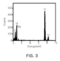
- FIG. 3 shows analysis result of the multilayer ceramic capacitor in an energy dispersive spectrometer (EDS) of a transmission electron microscope (TEM).
- EDS energy dispersive spectrometer
- TEM transmission electron microscope
- FIG. 1 is a schematic perspective view of a multilayer ceramic capacitor according to an embodiment of the present invention
- FIG. 2 is a schematic cross-sectional view taken along line A-A′ of FIG. 1 .
- a multilayer ceramic capacitor 100 includes a ceramic body 110 , first and second inner electrodes 120 a and 120 b provided inside the ceramic body 110 , and first and second outer electrodes 130 a and 130 b electrically connected to the first and second inner electrodes 120 a and 120 b.
- the ceramic body 110 includes a capacitive part 110 B and passivation layers 110 A provided on the top and bottom surfaces of the capacitive part 110 B.
- the capacitive part 110 B has a structure in which a plurality of dielectric layers 111 and a plurality of first and second inner electrodes 120 a and 120 b are alternately laminated.
- the first and second inner electrodes 120 a and 120 b are a pair of electrodes having different polarities.
- the first and second inner electrodes 120 a and 120 b are disposed to face each other along a direction of lamination of the dielectric layers 111 , and are electrically insulated from each other by the dielectric layers 111 . Ends of the first and second inner electrodes 120 a and 120 b are alternately and respectively exposed in a direction of lamination of the dielectric layers 111 .
- the exposed ends of the first and second inner electrodes 120 a and 120 b are electrically connected to the first and second outer electrodes 130 a and 130 b , respectively.
- the dielectric layer 111 of the capacitive part 110 B may be formed of a ceramic material having high permittivity.
- the dielectric layers 111 may be formed of, but are not limited to, a barium titanate (BaTiO 3 )-based ceramic, a lead complex perovskite-based ceramic, or a strontium titanate (SrTiO 3 )-based ceramic.
- the passivation layers 110 A may be formed on either or both of the top and bottom surfaces of the capacitive part 110 B. In this embodiment, the passivation layers 110 A are formed on both of the top and bottom surfaces of the capacitive part 110 B.
- the passivation layers 110 A may be formed of a ceramic material having high permittivity.
- the passivation layers 110 A may be formed of, but are not limited to, a barium titanate (BaTiO 3 )-based ceramic, a lead complex perovskite-based ceramic, or a strontium titanate (SrTiO 3 )-based ceramic.
- the passivation layer 110 A includes 0.5-10 wt % of Mg.
- Mg may be added in a manner known to those skilled in the art, without particular limitations.
- Mg may be added in a form of MgCO 3 or MgO.
- Mg existing in the passivation layer 110 A moves to the inner electrode during firing to thereby form oxide represented by Ni—Mg—O.
- the oxide represented by Ni—Mg—O is more stable than oxide represented by Ni—O.
- Mg existing in the passivation layer When a content of Mg existing in the passivation layer is less than 0.5 wt %, the adhesiveness between the passivation layer and the inner electrode may be weakened. When a content of Mg existing in the passivation is more than 10 wt %, Mg may degrade the dielectric characteristic of the capacitive part.
- the passivation layer may include glass.
- the glass includes Si, and may include an alkaline metal or an alkaline earth metal together with Si.
- a content of Si may be in the range of 0.5-15 wt %. When the content of Si is less than 0.5 wt %, the adhesiveness between the passivation layer and the inner electrode may be weakened. When the content of Si is more than 15 wt %, the Si content of the passivation layer may degrade the dielectric characteristic of the capacitive part.
- the passivation 110 A may be formed to be thicker than the dielectric layer 111 of the capacitive part 110 B.
- the dielectric layer 111 of the capacitive part 110 B may be 2 ⁇ m or less and laminated with approximately 25 layers or more, and thus, the thickness of the capacitive part 110 B may be in the range of 50-2,000 ⁇ m. In this case, the thickness of the passivation layer 110 A may be in the range of 10-100 ⁇ m.
- the first and second inner electrodes 120 a and 120 b are formed of a conductive metal, for example, Ni or a Ni alloy.
- the Ni alloy may include Mn, Cr, Co or Al together with Ni.
- One or more inner electrodes disposed at both ends of the ceramic body in a direction of lamination include oxide represented by Ni—Mg—O.
- the both ends in the direction of lamination refer to regions contacting the passivation layers 110 A in the capacitive part 110 B.
- Only the outermost inner electrode among the plurality of inner electrodes may an oxidized inner electrode including an oxide represented by Ni—Mg—O.
- one or more inner electrodes disposed inside the capacitive part, not the outermost position of the capacitive part may include the oxide represented by Ni—Mg—O.
- the oxidation rate of the outermost inner electrode is highest, and the oxidation rate of the inner electrodes is gradually reduced toward the inside of the capacitive part.
- the inner electrode disposed at the outermost ends in the direction of lamination may include 30% or more of the oxide represented by Ni—Mg—O.
- the number of the oxidized inner electrodes and the oxidation rate of the inner electrodes may be determined by adjusting a level of oxygen partial pressure during firing.
- the oxidized inner electrode has excellent adhesiveness with the passivation layer, thereby improving the adhesiveness between the capacitive part and the passivation layer. Accordingly, crack and blister occurrence rates between the capacitive part and the passivation part are reduced.
- the oxidized inner electrode prevents the penetration of moisture from the outside, thereby improving the humidity resistance of the multilayer ceramic capacitor.
- the first and second outer electrodes 130 a and 130 b are formed of, but are not limited to, a conductive metal.
- the first and second outer electrodes 130 a and 130 b may include copper.
- a plurality of ceramic green sheets to be laminated in a capacitive part are prepared. Specifically, a slurry is formed by mixing a ceramic powder, a binder, and a solvent, and the slurry is made into a sheet having a thickness of several ⁇ m by a doctor blade method.
- a paste for an inner electrode is coated on the ceramic green sheets to form first and second inner electrode patterns.
- the first and second inner electrode patterns may be formed by a screen printing process.
- the paste for an inner electrode may be formed by dispersing a Ni or Ni alloy powder into an organic binder and an organic solvent.
- the Ni alloy may include Mn, Cr, Co, or Al together with Ni.
- the organic binder may use a binder known in the art to which the invention pertains.
- the organic binder may use, but is not limited to, a cellulose-based resin, an epoxy resin, an aryl resin, an acryl resin, a phenol-formaldehyde resin, an unsaturated polyester resin, a polycarbonate resin, a polyamide resin, a polyimide resin, an alkyd resin, or a rosin ester.
- the organic solvent may also use an organic solvent known in the art to which the invention pertains.
- the organic solvent may use, but is not limited to, butyl carbitol, butyl carbitol acetate, turpentine oil, ⁇ -terebineol, ethyl cellosolve, or butyl phthalate.
- the ceramic green sheets in which the first and second inner electrode patterns are formed are laminated and pressed in a direction of lamination to thereby attach the laminated ceramic green sheets to the paste for an inner electrode. In this way, a capacitive part in which the ceramic green sheets and the paste for an inner electrode are alternately laminated is manufactured.
- a plurality of ceramic green sheets to be laminated on the top and bottom surfaces of the capacitive part are prepared.
- a slurry is formed by mixing a ceramic powder, Mg, an organic binder, and a solvent, and the slurry is made into a sheet having a thickness of several ⁇ m by a doctor blade method.
- the content of Mg is in the range of 0.5-10 wt % with respect to the entire composition.
- a Si-containing glass may be added. In this case, the content of Si may be in the range of 0.5-15 wt % with respect to the entire composition.
- the ceramic green sheets are laminated in the capacitive part to thereby obtain a multilayer ceramic body in which a passivation layer is formed.
- the multilayer ceramic body is cut to form a chip in each region corresponding to a single capacitor.
- the multilayer ceramic body is cut such that ends of the first and second inner electrode patterns are alternately and respectively exposed to the ends thereof.
- a ceramic sintered body is manufactured by firing the chips under a condition that oxidizes one or more inner electrodes disposed at both ends of the multilayer ceramic body in the direction of lamination.
- the firing temperature may be 1,200° C.
- the number of the oxidized inner electrodes and the oxidation rate of the inner electrodes may be adjusted according to the oxygen partial pressure.
- first and second outer electrodes are formed to cover the ends of the ceramic sintered body and to be electrically connected to the first and second inner electrodes which are exposed to the ends of the ceramic sintered body.
- the surfaces of the outer electrodes may be plated with Ni or Sn.
- the multilayer ceramic capacitor manufactured according to the embodiment of the present invention was cut in a direction of lamination, and the cut surface was polished. Components in the cut surface were analyzed using an energy dispersive spectrometer (EDS) of a transmission electron microscope (TEM). The analysis results are illustrated in FIG. 3 . It can be seen from FIG. 3 that the oxide represented by Ni—Mg—O exists.
- multilayer ceramic capacitors were manufactured while changing the composition of the passivation layer, and the blister occurrence rate and the crack occurrence rate of the manufactured multilayer ceramic capacitors were measured.
- the multilayer ceramic capacitor includes the oxidized inner electrode in the capacitive part adjacent to the passivation layer.
- the oxidized inner electrode includes oxide represented by Ni—Mg—O, which has excellent adhesiveness with the passivation layer. Therefore, the adhesiveness between the capacitive part and the passivation layer is improved, thereby reducing the crack occurrence rate and the blister occurrence rate between the capacitive part and the passivation layer.
- the oxidized inner electrode prevents the penetration of moisture from the outside, thereby improving the humidity resistance of the multilayer ceramic capacitor.
Landscapes
- Engineering & Computer Science (AREA)
- Power Engineering (AREA)
- Manufacturing & Machinery (AREA)
- Microelectronics & Electronic Packaging (AREA)
- Chemical & Material Sciences (AREA)
- Materials Engineering (AREA)
- Ceramic Engineering (AREA)
- Inorganic Chemistry (AREA)
- Ceramic Capacitors (AREA)
- Fixed Capacitors And Capacitor Manufacturing Machines (AREA)
Applications Claiming Priority (2)
| Application Number | Priority Date | Filing Date | Title |
|---|---|---|---|
| KR1020090134458A KR101079478B1 (ko) | 2009-12-30 | 2009-12-30 | 적층 세라믹 커패시터 및 그 제조방법 |
| KR10-2009-0134458 | 2009-12-30 |
Publications (2)
| Publication Number | Publication Date |
|---|---|
| US20110157768A1 US20110157768A1 (en) | 2011-06-30 |
| US8331079B2 true US8331079B2 (en) | 2012-12-11 |
Family
ID=44187269
Family Applications (1)
| Application Number | Title | Priority Date | Filing Date |
|---|---|---|---|
| US12/941,589 Active 2031-07-19 US8331079B2 (en) | 2009-12-30 | 2010-11-08 | Multilayer ceramic capacitor and method of manufacturing the same |
Country Status (3)
| Country | Link |
|---|---|
| US (1) | US8331079B2 (ja) |
| JP (1) | JP2011139028A (ja) |
| KR (1) | KR101079478B1 (ja) |
Cited By (1)
| Publication number | Priority date | Publication date | Assignee | Title |
|---|---|---|---|---|
| US20140192453A1 (en) * | 2013-01-09 | 2014-07-10 | Samsung Electro-Mechanics Co., Ltd. | Conductive resin composition, multilayer ceramic capacitor having the same, and method of manufacturing the multilayer ceramic capacitor |
Families Citing this family (12)
| Publication number | Priority date | Publication date | Assignee | Title |
|---|---|---|---|---|
| JP5360425B2 (ja) * | 2010-04-08 | 2013-12-04 | 株式会社村田製作所 | 回路モジュール、および回路モジュールの製造方法 |
| KR101422920B1 (ko) * | 2012-09-06 | 2014-07-23 | 삼성전기주식회사 | 적층 세라믹 커패시터 및 그 제조방법 |
| KR101412950B1 (ko) * | 2012-11-07 | 2014-06-26 | 삼성전기주식회사 | 적층 세라믹 커패시터 |
| JP6117557B2 (ja) * | 2013-01-28 | 2017-04-19 | 京セラ株式会社 | 積層型電子部品 |
| JP6024483B2 (ja) * | 2013-01-29 | 2016-11-16 | 株式会社村田製作所 | 積層型セラミック電子部品 |
| JP5827358B2 (ja) * | 2014-03-10 | 2015-12-02 | 太陽誘電株式会社 | 積層セラミックコンデンサ |
| KR102089695B1 (ko) | 2014-04-30 | 2020-03-16 | 삼성전기주식회사 | 적층 세라믹 전자부품 및 그 제조방법 |
| DE102014112678A1 (de) * | 2014-09-03 | 2016-03-03 | Epcos Ag | Elektrisches Bauelement, Bauelementanordnung und Verfahren zur Herstellung eines elektrischen Bauelements sowie einer Bauelementanordnung |
| JP2018037492A (ja) | 2016-08-30 | 2018-03-08 | 太陽誘電株式会社 | 積層セラミックコンデンサ及びその製造方法 |
| JP6954519B2 (ja) * | 2017-04-11 | 2021-10-27 | 太陽誘電株式会社 | 積層セラミックコンデンサ |
| WO2020018651A1 (en) * | 2018-07-18 | 2020-01-23 | Avx Corporation | Varistor passivation layer and method of making the same |
| CN113410050B (zh) * | 2021-05-27 | 2022-07-22 | 潮州三环(集团)股份有限公司 | 一种镍电极组合物及其制备方法和应用 |
Citations (16)
| Publication number | Priority date | Publication date | Assignee | Title |
|---|---|---|---|---|
| US5142437A (en) * | 1991-06-13 | 1992-08-25 | Ramtron Corporation | Conducting electrode layers for ferroelectric capacitors in integrated circuits and method |
| JPH113834A (ja) | 1996-07-25 | 1999-01-06 | Murata Mfg Co Ltd | 積層セラミックコンデンサおよびその製造方法 |
| JPH11162777A (ja) | 1997-11-28 | 1999-06-18 | Kyocera Corp | 積層セラミックコンデンサ |
| JP2000340450A (ja) | 1999-05-26 | 2000-12-08 | Kyocera Corp | 積層セラミックコンデンサおよびその製造方法 |
| US6381118B1 (en) * | 1999-07-22 | 2002-04-30 | Tdk Corporation | Ceramic electronic component having electronic component containing cuprous oxide |
| JP2002270458A (ja) | 2001-03-08 | 2002-09-20 | Murata Mfg Co Ltd | 積層セラミックコンデンサ |
| US6587327B1 (en) * | 2002-05-17 | 2003-07-01 | Daniel Devoe | Integrated broadband ceramic capacitor array |
| US6639267B2 (en) * | 2001-08-30 | 2003-10-28 | Micron Technology, Inc. | Capacitor dielectric having perovskite-type crystalline structure |
| US7123467B2 (en) * | 2001-09-28 | 2006-10-17 | Epcos Ag | Electroceramic component comprising a plurality of contact surfaces |
| KR20070014052A (ko) | 2005-07-26 | 2007-01-31 | 다이요 유덴 가부시키가이샤 | 적층 세라믹 콘덴서 및 그 제조 방법 |
| KR20080032883A (ko) | 2006-10-11 | 2008-04-16 | 삼성전기주식회사 | 적층 세라믹 캐패시터 |
| JP2009182011A (ja) | 2008-01-29 | 2009-08-13 | Taiyo Yuden Co Ltd | 積層セラミックコンデンサ及びその製造方法 |
| KR20090102120A (ko) | 2008-03-25 | 2009-09-30 | 삼성전기주식회사 | 적층 세라믹 캐패시터 |
| JP2009224569A (ja) | 2008-03-17 | 2009-10-01 | Samsung Electro Mech Co Ltd | 積層セラミックスキャパシタ |
| US20100157505A1 (en) * | 2007-07-06 | 2010-06-24 | Thomas Feichtinger | Multilayer Electrical Component |
| US8194390B2 (en) * | 2009-12-24 | 2012-06-05 | Samsung Electro-Mechanics Co., Ltd. | Multilayer ceramic capacitor and fabricating method thereof |
-
2009
- 2009-12-30 KR KR1020090134458A patent/KR101079478B1/ko active IP Right Grant
-
2010
- 2010-11-05 JP JP2010249020A patent/JP2011139028A/ja active Pending
- 2010-11-08 US US12/941,589 patent/US8331079B2/en active Active
Patent Citations (16)
| Publication number | Priority date | Publication date | Assignee | Title |
|---|---|---|---|---|
| US5142437A (en) * | 1991-06-13 | 1992-08-25 | Ramtron Corporation | Conducting electrode layers for ferroelectric capacitors in integrated circuits and method |
| JPH113834A (ja) | 1996-07-25 | 1999-01-06 | Murata Mfg Co Ltd | 積層セラミックコンデンサおよびその製造方法 |
| JPH11162777A (ja) | 1997-11-28 | 1999-06-18 | Kyocera Corp | 積層セラミックコンデンサ |
| JP2000340450A (ja) | 1999-05-26 | 2000-12-08 | Kyocera Corp | 積層セラミックコンデンサおよびその製造方法 |
| US6381118B1 (en) * | 1999-07-22 | 2002-04-30 | Tdk Corporation | Ceramic electronic component having electronic component containing cuprous oxide |
| JP2002270458A (ja) | 2001-03-08 | 2002-09-20 | Murata Mfg Co Ltd | 積層セラミックコンデンサ |
| US6639267B2 (en) * | 2001-08-30 | 2003-10-28 | Micron Technology, Inc. | Capacitor dielectric having perovskite-type crystalline structure |
| US7123467B2 (en) * | 2001-09-28 | 2006-10-17 | Epcos Ag | Electroceramic component comprising a plurality of contact surfaces |
| US6587327B1 (en) * | 2002-05-17 | 2003-07-01 | Daniel Devoe | Integrated broadband ceramic capacitor array |
| KR20070014052A (ko) | 2005-07-26 | 2007-01-31 | 다이요 유덴 가부시키가이샤 | 적층 세라믹 콘덴서 및 그 제조 방법 |
| KR20080032883A (ko) | 2006-10-11 | 2008-04-16 | 삼성전기주식회사 | 적층 세라믹 캐패시터 |
| US20100157505A1 (en) * | 2007-07-06 | 2010-06-24 | Thomas Feichtinger | Multilayer Electrical Component |
| JP2009182011A (ja) | 2008-01-29 | 2009-08-13 | Taiyo Yuden Co Ltd | 積層セラミックコンデンサ及びその製造方法 |
| JP2009224569A (ja) | 2008-03-17 | 2009-10-01 | Samsung Electro Mech Co Ltd | 積層セラミックスキャパシタ |
| KR20090102120A (ko) | 2008-03-25 | 2009-09-30 | 삼성전기주식회사 | 적층 세라믹 캐패시터 |
| US8194390B2 (en) * | 2009-12-24 | 2012-06-05 | Samsung Electro-Mechanics Co., Ltd. | Multilayer ceramic capacitor and fabricating method thereof |
Non-Patent Citations (2)
| Title |
|---|
| Korean Office Action, w/ English translation thereof, issued in Korean Patent Application No. KR 10-2009-0134458 dated Apr. 21, 2011. |
| Office Action with English translation issued in corresponding JP Patent Application No. 2010-249020 dated May 25, 2012. |
Cited By (2)
| Publication number | Priority date | Publication date | Assignee | Title |
|---|---|---|---|---|
| US20140192453A1 (en) * | 2013-01-09 | 2014-07-10 | Samsung Electro-Mechanics Co., Ltd. | Conductive resin composition, multilayer ceramic capacitor having the same, and method of manufacturing the multilayer ceramic capacitor |
| US9019690B2 (en) * | 2013-01-09 | 2015-04-28 | Samsung Electro-Mechanics Co., Ltd. | Conductive resin composition, multilayer ceramic capacitor having the same, and method of manufacturing the multilayer ceramic capacitor |
Also Published As
| Publication number | Publication date |
|---|---|
| US20110157768A1 (en) | 2011-06-30 |
| KR101079478B1 (ko) | 2011-11-03 |
| JP2011139028A (ja) | 2011-07-14 |
| KR20110077797A (ko) | 2011-07-07 |
Similar Documents
| Publication | Publication Date | Title |
|---|---|---|
| US8331079B2 (en) | Multilayer ceramic capacitor and method of manufacturing the same | |
| US8248752B2 (en) | Multilayer ceramic capacitor | |
| US8390983B2 (en) | Multilayer ceramic capacitor | |
| US9384898B2 (en) | Multilayer ceramic capacitor and method of manufacturing the same | |
| US8345405B2 (en) | Multilayer ceramic capacitor | |
| KR102029468B1 (ko) | 적층 세라믹 전자부품 및 이의 제조방법 | |
| KR101983129B1 (ko) | 적층 세라믹 전자부품 및 이의 제조방법 | |
| KR101474138B1 (ko) | 적층 세라믹 전자 부품 및 그 제조 방법 | |
| US20130258546A1 (en) | Multilayer ceramic electronic component and fabrication method thereof | |
| US11164700B2 (en) | Multilayer capacitor | |
| KR20140081568A (ko) | 적층 세라믹 전자 부품 | |
| US20110141658A1 (en) | Multilayer ceramic capacitor | |
| CN112309718B (zh) | 多层电子组件 | |
| KR20190126610A (ko) | 적층형 커패시터 | |
| CN112151271B (zh) | 多层陶瓷电子组件 | |
| US11062847B2 (en) | Capacitor component and method for manufacturing the same | |
| US11735374B2 (en) | Multi-layered ceramic electronic component | |
| CN111009415B (zh) | 陶瓷电子组件 | |
| US11164702B2 (en) | Multi-layered ceramic electronic component having step absorption layer | |
| US11437193B2 (en) | Multilayer ceramic electronic component | |
| KR20230093745A (ko) | 적층 세라믹 전자부품 | |
| CN112242248A (zh) | 多层陶瓷电子组件 |
Legal Events
| Date | Code | Title | Description |
|---|---|---|---|
| AS | Assignment |
Owner name: SAMSUNG ELECTRO-MECHANICS CO., LTD., KOREA, REPUBL Free format text: ASSIGNMENT OF ASSIGNORS INTEREST;ASSIGNORS:HUR, KANG HEON;KIM, DOO YOUNG;HA, MUN SU;AND OTHERS;SIGNING DATES FROM 20100915 TO 20100916;REEL/FRAME:025331/0891 |
|
| STCF | Information on status: patent grant |
Free format text: PATENTED CASE |
|
| FEPP | Fee payment procedure |
Free format text: PAYOR NUMBER ASSIGNED (ORIGINAL EVENT CODE: ASPN); ENTITY STATUS OF PATENT OWNER: LARGE ENTITY |
|
| FPAY | Fee payment |
Year of fee payment: 4 |
|
| MAFP | Maintenance fee payment |
Free format text: PAYMENT OF MAINTENANCE FEE, 8TH YEAR, LARGE ENTITY (ORIGINAL EVENT CODE: M1552); ENTITY STATUS OF PATENT OWNER: LARGE ENTITY Year of fee payment: 8 |
|
| MAFP | Maintenance fee payment |
Free format text: PAYMENT OF MAINTENANCE FEE, 12TH YEAR, LARGE ENTITY (ORIGINAL EVENT CODE: M1553); ENTITY STATUS OF PATENT OWNER: LARGE ENTITY Year of fee payment: 12 |