US8115908B2 - Position measuring device and position measuring method in semiconductor single crystal manufacturing device - Google Patents
Position measuring device and position measuring method in semiconductor single crystal manufacturing device Download PDFInfo
- Publication number
- US8115908B2 US8115908B2 US12/676,431 US67643108A US8115908B2 US 8115908 B2 US8115908 B2 US 8115908B2 US 67643108 A US67643108 A US 67643108A US 8115908 B2 US8115908 B2 US 8115908B2
- Authority
- US
- United States
- Prior art keywords
- distance
- scanning
- light
- thermal shield
- melt
- Prior art date
- Legal status (The legal status is an assumption and is not a legal conclusion. Google has not performed a legal analysis and makes no representation as to the accuracy of the status listed.)
- Active, expires
Links
Images


Classifications
-
- C—CHEMISTRY; METALLURGY
- C30—CRYSTAL GROWTH
- C30B—SINGLE-CRYSTAL GROWTH; UNIDIRECTIONAL SOLIDIFICATION OF EUTECTIC MATERIAL OR UNIDIRECTIONAL DEMIXING OF EUTECTOID MATERIAL; REFINING BY ZONE-MELTING OF MATERIAL; PRODUCTION OF A HOMOGENEOUS POLYCRYSTALLINE MATERIAL WITH DEFINED STRUCTURE; SINGLE CRYSTALS OR HOMOGENEOUS POLYCRYSTALLINE MATERIAL WITH DEFINED STRUCTURE; AFTER-TREATMENT OF SINGLE CRYSTALS OR A HOMOGENEOUS POLYCRYSTALLINE MATERIAL WITH DEFINED STRUCTURE; APPARATUS THEREFOR
- C30B15/00—Single-crystal growth by pulling from a melt, e.g. Czochralski method
- C30B15/20—Controlling or regulating
- C30B15/22—Stabilisation or shape controlling of the molten zone near the pulled crystal; Controlling the section of the crystal
- C30B15/26—Stabilisation or shape controlling of the molten zone near the pulled crystal; Controlling the section of the crystal using television detectors; using photo or X-ray detectors
-
- C—CHEMISTRY; METALLURGY
- C30—CRYSTAL GROWTH
- C30B—SINGLE-CRYSTAL GROWTH; UNIDIRECTIONAL SOLIDIFICATION OF EUTECTIC MATERIAL OR UNIDIRECTIONAL DEMIXING OF EUTECTOID MATERIAL; REFINING BY ZONE-MELTING OF MATERIAL; PRODUCTION OF A HOMOGENEOUS POLYCRYSTALLINE MATERIAL WITH DEFINED STRUCTURE; SINGLE CRYSTALS OR HOMOGENEOUS POLYCRYSTALLINE MATERIAL WITH DEFINED STRUCTURE; AFTER-TREATMENT OF SINGLE CRYSTALS OR A HOMOGENEOUS POLYCRYSTALLINE MATERIAL WITH DEFINED STRUCTURE; APPARATUS THEREFOR
- C30B15/00—Single-crystal growth by pulling from a melt, e.g. Czochralski method
- C30B15/14—Heating of the melt or the crystallised materials
-
- C—CHEMISTRY; METALLURGY
- C30—CRYSTAL GROWTH
- C30B—SINGLE-CRYSTAL GROWTH; UNIDIRECTIONAL SOLIDIFICATION OF EUTECTIC MATERIAL OR UNIDIRECTIONAL DEMIXING OF EUTECTOID MATERIAL; REFINING BY ZONE-MELTING OF MATERIAL; PRODUCTION OF A HOMOGENEOUS POLYCRYSTALLINE MATERIAL WITH DEFINED STRUCTURE; SINGLE CRYSTALS OR HOMOGENEOUS POLYCRYSTALLINE MATERIAL WITH DEFINED STRUCTURE; AFTER-TREATMENT OF SINGLE CRYSTALS OR A HOMOGENEOUS POLYCRYSTALLINE MATERIAL WITH DEFINED STRUCTURE; APPARATUS THEREFOR
- C30B29/00—Single crystals or homogeneous polycrystalline material with defined structure characterised by the material or by their shape
- C30B29/02—Elements
- C30B29/06—Silicon
Definitions
- the present invention relates to a position measuring device and a position measuring method in a semiconductor single crystal manufacturing device, and in particular relates to a position measuring device and a position measuring method applied to a semiconductor single crystal manufacturing device for manufacturing a semiconductor single crystal while measuring a distance between a thermal shield and a melt or/and a liquid level of the melt and performing control so that the measurement becomes a desired value.
- a silicon single crystal is manufactured by being pulled up and grown based on CZ (Czochralski method).
- FIG. 1 shows a configuration example of a silicon single crystal manufacturing device 1 .
- a CZ furnace 2 is internally provided with a quartz crucible 3 for melting a polycrystalline silicon raw material and housing it as a melt 5 .
- Polycrystalline silicon (Si) is heated and melted in the quartz crucible 3 .
- a pulling mechanism 4 is operated and the silicon single crystal 10 is pulled up from the melt 5 .
- the quartz crucible 3 is rotated with a rotational axis 15 .
- the rotational axis 15 can be driven in the vertical direction, and is able to move the quartz crucible 3 vertically to an arbitrary crucible position, and thereby adjust a surface 5 a of the melt 5 , namely, the liquid level H of the melt 5 .
- thermal shield 8 heat radiation plate, gas straightening tube
- melt 5 is provided above the melt 5 and around the silicon single crystal 10 .
- a rim 8 a is provided to the lower end of the thermal shield 8 .
- the thermal shield 8 guides, within the CZ furnace 2 , argon gas 7 as the carrier gas to be supplied from the upper side to the center of the melt surface 5 a , and further guides it to the peripheral edge of the melt surface 5 a by passing it through the melt surface 5 a .
- the argon gas 7 is thereafter discharged from an outlet provided to the lower part of the CZ furnace 2 together with the gas that evaporated from the melt 5 . Consequently, it is possible to stabilize the gas flow rate on the liquid level and maintain the oxygen that evaporated from the melt 5 in a stable state.
- the thermal shield 8 insulates and shields a seed crystal 14 and the silicon single crystal 10 grown from the seed crystal 14 from the heat radiation generated in the hot areas such as the quartz crucible 3 , the melt 5 , and a heater 9 .
- the thermal shield 8 also prevents impurities (for instance, silicon oxide) generated in the furnace from adhering to the silicon single crystal 10 and inhibiting the single crystal growth.
- the size of the distance L between the rim 8 a at the lower end of the thermal shield 8 and the melt surface 5 a (hereinafter referred to as the “thermal shield/liquid level distance”) can be adjusted by lifting and lowering the rotational axis 15 and changing the vertical position of the quartz crucible 3 .
- the distance L can also be adjusted by moving the thermal shield 8 in a vertical direction using a lifting and lowering device.
- Quality of the silicon single crystal 10 is conventionally known to fluctuate in accordance with the size of the melt liquid level H or the thermal shield/liquid level distance L during the pulling. Specifically, if the size of the melt liquid level H or the thermal shield/liquid level distance L changes during the pulling, parameters such as the temperature gradient in the axial direction of the silicon single crystal 10 consequently fluctuate, thereby causing the defect region distribution and oxygen concentration distribution of the silicon single crystal 10 to change, whereby the quality of the crystal also change.
- pulling conditions that is, the target value of the melt liquid level H for each pulling position or the target value of the thermal shield/liquid level distance L for each pulling position is predetermined according to the demanded specification.
- the actual values of the melt liquid level H or the actual values of the thermal shield/liquid level distance L are sequentially detected, these detected values are fed back, and control is performed to adjust the vertical position of the rotational axis 15 so that the deviation of the target value and the detected value becomes zero.
- the melt liquid level H or the thermal shield/liquid level distance L must be controlled to accurately coincide with the target value.
- the actual value of the melt liquid level H or the actual value of the thermal shield/liquid level distance L as the feedback amount to be detected during the control must constantly be measured with accuracy.
- FIG. 2 shows a configuration example of the distance measuring device for measuring the actual value of the melt liquid level H or the thermal shield/liquid level distance L for each pulling position.
- the distance measuring device 100 of FIG. 2 is configured by including light emitting means 110 for emitting a laser beam 101 , light scanning means 120 for scanning the laser beam 101 that is emitted from the light emitting means 110 along the radial direction of the quartz crucible 3 , light receiving means 130 for receiving the reflected light of the laser beam 101 that is emitted from the light emitting means 110 and used to perform scanning of the light scanning means 120 , and pulling distance measuring means 141 for measuring the thermal shield/liquid level distance L or/and the melt liquid level H based on the fixed scanning position during the pulling, the laser beam emitting position of the light emitting means 110 and the light receiving position of the light receiving means 130 , and according to the principle of triangulation.
- the light scanning means 120 is configured by including a mirror 121 for reflecting the laser beam 101 that is emitted from the light emitting means 110 , and a stepping motor 122 for changing the attitude angle of a light reflecting surface 121 a of the mirror 121 .
- the rotation angle ⁇ of the rotational axis 122 a of the stepping motor 122 and the scanning position of the laser beam 101 in the radial direction of the crucible 3 correspond one-to-one.
- the scanning position of the laser beam 101 in the crucible radial direction is represented as ⁇ .
- Patent Document 1 discloses a method of measuring the actual value of the melt liquid level H or the actual value of the thermal shield/liquid level distance L as follows.
- the stepping motor 122 is driven to position the optical scanning position ⁇ at the pulling position ⁇ 1 .
- the laser beam 101 is emitted from the light emitting means 110 and irradiated onto the melt level 5 a , and the laser beam that reflects off the melt level 5 a is received by the light receiving means 130 .
- the distance LS from the reference point to the liquid level 5 a of the melt 5 is sought and the melt liquid level H is measured based on the fixed scanning position ⁇ 1 during the pulling, the emitting position of the light emitting means 110 , and the light receiving position of the light receiving means 130 , and according to the principle of triangulation.
- the stepping motor 122 is driven to position the optical scanning position ⁇ at the pulling position ⁇ 2 .
- the laser beam 101 is emitted from the light emitting means 110 and irradiated onto the upper surface 8 b of the rim 8 a of the thermal shield 8 , and the laser beam that reflects off the rim upper surface 8 b is received by the light receiving means 130 .
- the distance S from the reference point to the upper surface 8 b of the rim 8 a of the thermal shield 8 is measured based on the fixed scanning position ⁇ 2 during the pulling, the emitting position of the light emitting means 110 , and the light receiving position of the light receiving means 130 , and according to the principle of triangulation.
- the thermal shield/liquid level distance L is calculated based on the obtained distance LS up to the liquid level 5 a of the melt 5 , the distance S up to the upper surface 8 b of the rim 8 a of the thermal shield 8 , and the thickness t of the rim 8 a of the thermal shield 8 .
- Patent Document 2 discloses a method of measuring the actual value of the melt liquid level H and the actual value of the thermal shield/liquid level distance L as follows.
- the stepping motor 122 is driven to position the optical scanning position ⁇ at the pulling position ⁇ 3 .
- the laser beam 101 is emitted from the light emitting means 110 to be reflected off the melt level 5 a
- the laser beam that reflects off the melt level 5 a is irradiated onto the lower surface 8 c of the rim 8 a of the thermal shield 8
- the laser beam that reflects off the rim lower surface 8 c is irradiated onto the melt level 5 a once again
- the laser beam that reflects off the melt level 5 a is received by the light receiving means 130 .
- the distance LS from the reference point to the liquid level 5 a of the melt 5 is sought and the melt liquid level H is measured based on the fixed scanning position ⁇ 3 during the pulling, the emitting position of the light emitting means 110 , and the light receiving position of the light receiving means 130 , and according to the principle of triangulation.
- the stepping motor 122 is driven to position the optical scanning position ⁇ at the pulling position ⁇ 4 .
- the laser beam 101 is emitted from the light emitting means 110 and irradiated onto the upper surface 8 b of the rim 8 a of the thermal shield 8 , and the laser beam that reflects off the rim upper surface 8 b is received by the light receiving means 130 .
- the distance S from the reference point to the upper surface 8 b of the rim 8 a of the thermal shield 8 is measured based on the fixed scanning position ⁇ 4 during the pulling, the emitting position of the light emitting means 110 , and the light receiving position of the light receiving means 130 , and according to the principle of triangulation.
- the thermal shield/liquid level distance L is calculated based on the thus obtained distance LS up to the liquid level 5 a of the melt 5 , the distance S up to the upper surface 8 b of the rim 8 a of the thermal shield 8 , and the thickness t of the rim 8 a of the thermal shield 8 .
- optical scanning positions ⁇ 1 , ⁇ 2 , ⁇ 3 , ⁇ 4 during the pulling are defined based on the reference optical scanning position ⁇ c.
- the reference optical scanning position ⁇ c is the edge 8 e of the rim 8 a of the thermal shield 8 .
- Patent Document 2 discloses the position measuring algorithm for measuring the optical scanning position ⁇ c of the edge 8 e of the rim 8 a of the thermal shield 8 . This position measuring principle is explained with reference to FIG. 4 . This position measuring algorithm is performed, for instance, between the respective batches, during the disassembly or cleaning of the CZ furnace 2 , or midway during the pulling process.
- the distance between the reference point and the reflection point is sequentially measured for each prescribed interval ⁇ 1 based on the sequential optical scanning position, the emitting position of the light emitting means 110 , and the light receiving position of the light receiving means 130 , and according to the principle of triangulation while scanning the laser beam 101 by the light scanning means 120 in the radial direction of the crucible 3 .
- the measured distance changes from a size corresponding to the distance between the reference point and the melt 5 to a size corresponding to the distance between the reference point and the rim 8 a of the thermal shield 8 .
- the laser beam 101 is reflected off the edge 8 e of the rim 8 a of the thermal shield 8 at the optical scanning position ⁇ c at the point in time that the change is determined.
- the positions ⁇ 1 , ⁇ 2 , ⁇ 3 , ⁇ 4 of the direction for scanning the laser beam 101 during the pulling are defined as reference based on the optical scanning position ⁇ c when it is determined that the laser beam 101 reflected off the edge 8 e of the rim 8 a of the thermal shield 8 .
- Noise as used herein refers to the ghost (stray light) caused by the scattered light other than the melt mirror reflection.
- the position measuring algorithm performs the position measurement operation with high efficiency, the optical scanning is performed at high speed by driving the stepping motor 122 at high speed, and the distance measurement is performed at an interval of a relatively long cycle ⁇ 1 ( FIG. 5A ).
- the edge position is often erroneously measured as the position ⁇ b of the upper surface 8 b of the rim 8 a .
- the edge position varies in the range ⁇ beyond the edge 8 e as shown in FIG. 5B .
- the fixed scanning positions ⁇ 1 , ⁇ 2 , ⁇ 3 , ⁇ 4 during the measurement conducted by defining the edge position ⁇ c as the reference also vary.
- the upper surface 8 b of the rim 8 a of the thermal shield 8 is never flat, and the irregularity differs and the height differs by location.
- the distance S from the reference point to the upper surface 8 b of the rim 8 a of the thermal shield 8 also varies.
- FIG. 6A is experimental data showing that the measurement S varies in each batch.
- the edge position is measured for each batch, the optical scanning positions ⁇ 2 , ⁇ 4 based on the edge position were rewritten for each batch, and the laser beam 101 is emitted by fixing the positions to the rewritten optical scanning positions ⁇ 2 , ⁇ 4 to measure the S value for each batch.
- the horizontal axis of the histogram is the deviation from the average value of the S measurement, and the average value is set to 0. Meanwhile, the vertical axis shows the frequency.
- the distance S value varied within the range of ⁇ 3 mm of the average value.
- the S measurement varies as described above, the measurement of the thermal shield/liquid level distance L consequently varies, and it is difficult to stably control the pulling and growth of the silicon single crystal upon feeding back the actual position of the thermal shield/liquid level distance L. Consequently, the quality of the pulled and grown silicon single crystal 10 may vary, and it may become difficult to provide a product of stable specification.
- edge position ⁇ c cannot be accurately sought, it becomes difficult to accurately irradiate the laser beam 101 onto the target position of the upper surface 8 b of the rim 8 a of the thermal shield 8 upon defining the irradiation direction of the laser beam 101 based on the edge position ⁇ c, and it becomes difficult to irradiate the laser beam 101 onto the target position of the melt surface 5 a . Consequently, it may become difficult to perform the distance measurement shown in FIG. 2 or to perform the distance measurement shown in FIG. 3 .
- the thermal shield 8 and the silicon single crystal 10 are narrow, or if the length of the crucible radial direction of the upper surface 8 b of the rim 8 a of the thermal shield 8 is short, it becomes even more difficult.
- the present invention is made in view of the foregoing circumstances, and an object thereof is to measure the edge position ⁇ c accurately without variation while performing the position measurement processing of the edge position ⁇ c of the thermal shield 8 is performed in a short period of time and at high working efficiency.
- a first aspect of the present invention provides position measuring device applied to a semiconductor single crystal manufacturing device for manufacturing a semiconductor crystal by pulling up and growing a semiconductor single crystal from a melt housed in a furnace crucible, which includes: a thermal shield located above the melt and provided around the semiconductor single crystal, and having a rim at the lower end thereof; light emitting means for emitting light; light scanning means for performing scanning of the light emitted from the light emitting means along a radial direction of the crucible; light receiving means for receiving reflected light of the light emitted from the light emitting means and used to perform scanning by the light scanning means; first distance measuring means for sequentially measuring a distance between a reference point and a reflection point for each prescribed first scanning interval based on a sequential optical scanning position, an emitting position of the light emitting means, and a light receiving position of the light receiving means and according to a principle of triangulation while performing light scanning; first determination means for determining whether the distance measured by the first distance measuring means changes from a size corresponding to a distance between
- a second aspect of the present invention provides the position measuring device applied to a semiconductor single crystal manufacturing device according to first aspect of the present invention for manufacturing a semiconductor single crystal while measuring a distance between a thermal shield and a melt or/and a liquid level of the melt during pulling of the semiconductor single crystal and performing control so that the measurement becomes a desired value, which further includes: pulling distance measuring means for fixing as the pulling position the position in the direction of scanning light during the pulling of the semiconductor single crystal, and measuring the distance between the thermal shield and the melt or/and the liquid level of the melt based on the fixed scanning position during the pulling, the emitting position of the light emitting means, and the light receiving position of the light receiving means and according to the principle of triangulation, wherein the fixed scanning position during the pulling is defined based on the optical scanning position when the edge position judgment means judges that light is reflected by the edge of the rim of the thermal shield.
- a third aspect of the present invention provides the position measuring device applied to a semiconductor single crystal manufacturing device according to the second aspect of the present invention, wherein the fixed scanning position during the pulling is defined so that light traces a path of reflecting off the liquid level of the melt and the side surface of the rim of the thermal shield, respectively.
- a fourth aspect of the present invention provides the position measuring device applied to a semiconductor single crystal manufacturing device according to the first aspect of the present invention, wherein the light scanning means includes a mirror for reflecting the light emitted from the light emitting means, and an actuator for changing an attitude angle of a light reflecting surface of the mirror, and performs scanning of light by driving the actuator and changing the attitude angle of the light reflecting surface of the mirror.
- the light scanning means includes a mirror for reflecting the light emitted from the light emitting means, and an actuator for changing an attitude angle of a light reflecting surface of the mirror, and performs scanning of light by driving the actuator and changing the attitude angle of the light reflecting surface of the mirror.
- a fifth aspect of the present invention provides the position measuring device applied to a semiconductor single crystal manufacturing device according to the first aspect of the present invention or the fourth aspect of the present invention, wherein the light scanning means performs light scanning by using a stepping motor as the actuator, and the second distance measuring means measures the distance between the reference point and the reflection point each time the stepping motor makes one step rotation.
- a sixth aspect of the present invention provides a position measuring method applied to a semiconductor single crystal manufacturing device for manufacturing a semiconductor crystal by pulling up and growing a semiconductor single crystal from a melt housed in a furnace crucible, the method implementing position measurement processing which includes: a first distance measuring step of sequentially measuring a distance between a reference point and a reflection point of light for each prescribed first scanning interval based on a sequential optical scanning position, an emitting position of light, and a light receiving position of light and according to a principle of triangulation while performing scanning of the light along a radial direction of the crucible; a first determination step of determining whether the distance measured in the first distance measuring step changes from a size corresponding to a distance between the reference point and the melt to a size corresponding to a distance between the reference point and a rim of a thermal shield, or changes from a size corresponding to the distance between the reference point and the rim of the thermal shield to a size corresponding to the distance between the reference point and the melt; a second distance measuring step
- a seventh aspect of the present invention provides the position measuring method applied to a semiconductor single crystal manufacturing device according to the sixth aspect of the present invention manufacturing a semiconductor single crystal while measuring a distance between a thermal shield and a melt or/and a liquid level of the melt during pulling of the semiconductor single crystal and performing control so that the measurement becomes a desired value, further including: a step of defining a position of a direction of scanning light during the pulling based on an optical scanning position when determination is made in the edge position judgment step that light is reflected by the edge of the rim of the thermal shield; and a pulling distance measuring step of fixing the position of the direction of scanning light during the pulling of the semiconductor single crystal, and measuring the distance between the thermal shield and the melt or/and the liquid level of the melt based on the fixed scanning position during the pulling, the emitting position of light emitting means, and the light receiving position of light receiving means and according to the principle of triangulation.
- An eighth aspect of the present invention according to the seventh aspect of the present invention is that the fixed scanning position during the pulling is defined so that light traces a path of reflecting off the liquid level of the melt and the side surface of the rim of the thermal shield, respectively.
- the first aspect of the present invention is now explained with reference to the configuration diagram of FIG. 2 , the position measuring algorithm shown in FIG. 7 and FIG. 8 , and with reference to FIG. 9A , FIG. 9B , and FIG. 9C .
- the first distance measuring means 142 sequentially measures the distance d between the reference point and the reflection point for each prescribed first scanning interval ⁇ 1 based on the sequential optical scanning position, the emitting position of the light emitting means 110 , and the light receiving position of the light receiving means 130 , and according to the principle of triangulation while scanning the laser beam 101 in the radial direction of the crucible 3 by the light scanning means 120 ( FIG. 9A ; step 204 ).
- the first determination means 143 determines whether the distance d measured by the first distance measuring means 142 changes from a size corresponding to the distance da between the reference point and the melt 5 to a size corresponding to the distance db between the reference point and the rim 8 a of the thermal shield 8 (step 205 ).
- the optical scanning position ⁇ is returned a predetermined amount ⁇ in the opposite direction B of the scanning direction A ( FIG. 9A ; step 210 ).
- the second distance measuring means 144 sequentially measures the distance d between the reference point and the reflection point for each second scanning interval ⁇ 2 that is shorter than the first scanning interval ⁇ 1 based on the sequential optical scanning position, the emitting position of the light emitting means, and the light receiving position of the light receiving means, and according to the principle of triangulation while re-scanning the laser beam 101 from the returned optical scanning position ⁇ rs ( FIG. 9B ); step 211 ).
- the second determination means 145 determines whether the distance d measured by the second distance measuring means 144 changes from a size corresponding to the distance da between the reference point and the melt 5 to a size corresponding to the distance db between the reference point and the rim 8 a of the thermal shield 8 (step 212 ).
- step 212 determination of YES
- the distance measurement can be resumed before the edge position.
- the second distance measurement is performed at an interval of a relatively short cycle ⁇ 2 in comparison to the initial distance measurement ( FIG. 9A ).
- the irradiation point of the laser beam 101 does not deviate from the edge 8 e and it moves to the back of the upper surface 8 b of the rim 8 a , and the position of the edge 8 e can be measured without error.
- the section of conducting distance measurement for each short interval ⁇ 2 is a short section up to the re-detection of the edge position from the position ⁇ rs at which the optical scanning position is returned a predetermined amount ( FIG. 9B ; limit value (40 pulses)), and otherwise the distance measurement is conducted for each long interval ⁇ 1 and the processing is performed at high speed.
- the position measurement processing can be completed in a short period of time and the operation can be performed with high efficiency.
- the edge position ⁇ c can be measured accurately without variation while performing the position measurement processing of the edge position ⁇ c of the thermal shield 8 in a short period of time and with high working efficiency.
- the positions ⁇ 1 , ⁇ 2 , ⁇ 3 , ⁇ 4 of the direction of scanning the laser beam 101 during the pulling are defined based on the optical scanning position ⁇ c when it is determined that the laser beam 101 is reflected off the edge 8 e of the rim 8 a of the thermal shield 8 (step 221 ).
- the position of the direction of scanning the laser beam 101 is fixed to the pulling positions ⁇ 1 , ⁇ 2 , ⁇ 3 , ⁇ 4 , and the distance L between the thermal shield and the melt or/and the liquid level H of the melt are measures based on the fixed scanning position during the pulling, the emitting position of the light emitting means, and the light receiving position of the light receiving means, and according to the principle of triangulation.
- the silicon single crystal 10 is manufactured while controlling the measurements L, H to become a desired value.
- the edge position ⁇ c can be accurately measured without variation for each batch, and the distance S from the reference point to the upper surface 8 b of the rim 8 a of the thermal shield 8 can be accurately measured without variation.
- the edge position ⁇ c can be sought accurately, it is possible to accurately irradiate the laser beam 101 onto the target position of the upper surface 8 b of the rim 8 a of the thermal shield 8 upon accurately defining the irradiation direction of the laser beam 101 based on the edge position ⁇ c, and it is also possible to accurately irradiate the laser beam 101 onto the target position of the melt surface 5 a . Consequently, even if the distance D between the thermal shield 8 and the silicon single crystal 10 is narrow or if the length of the upper surface 8 b of the rim 8 a of the thermal shield 8 in the crucible radial direction is short, it is possible to accurately irradiate the laser beam 101 onto the target position, and the distance measurement shown in FIG. 2 can be conducted easily. Similarly, the distance measurement shown in FIG. 3 can also be conducted easily.
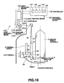
- the fixed scanning positions ⁇ 5 , ⁇ 6 during the pulling are defined so that the laser beam 101 traces a path of reflecting off the liquid level 5 a of the melt 5 and the side surface 8 d of the rim 8 a of the thermal shield 8 , respectively.
- the stepping motor 122 is driven to position the optical scanning position ⁇ at the pulling position ⁇ 5 .
- the laser beam 101 is emitted from the light emitting means 110 and irradiated onto the side surface 8 d of the rim 8 a of the thermal shield 8 , the laser beam that reflects off the rim side surface 8 d is irradiated onto the melt level 5 a , and the laser beam that reflects off the melt level 5 a is received by the light receiving means 130 .
- the distance LS from the reference point to the liquid level 5 a of the melt 5 is sought and the melt liquid level H is measured based on the fixed scanning position ⁇ 5 during the pulling, the emitting position of the light emitting means 110 , and the light receiving position of the light receiving means 130 , and according to the principle of triangulation.
- the stepping motor 122 is driven to position the optical scanning position ⁇ at the pulling position ⁇ 6 .
- the laser beam 101 is emitted from the light emitting means 110 and irradiated onto the upper surface 8 b of the rim 8 a of the thermal shield 8 , and the laser beam that reflects off the rim upper surface 8 b is received by the light receiving means 130 .
- the distance S from the reference point to the upper surface 8 b of the rim 8 a of the thermal shield 8 is measured based on the fixed scanning position ⁇ 6 during the pulling, the emitting position of the light emitting means 110 , and the light receiving position of the light receiving means 130 , and according to the principle of triangulation.
- the thermal shield/liquid level distance L is calculated based on the thus obtained distance LS up to the liquid level 5 a of the melt 5 , the distance S up to the upper surface 8 b of the rim 8 a of the thermal shield 8 , and the thickness t of the rim 8 a of the thermal shield 8 .
- the edge position ⁇ c can be sought accurately, it is be possible to accurately define the fixed scanning position ⁇ 5 during the pulling based on the edge position ⁇ c, and thereby accurately irradiating the laser beam 101 onto the target position of the upper surface 8 b of the rim 8 a of the thermal shield 8 upon accurately defining the irradiation direction of the laser beam 101 . Consequently, even with the distance measuring method shown in FIG. 10 where the laser beam 101 must be irradiated onto an extremely narrow side surface 8 d of the rim 8 a of the thermal shield 8 , the laser beam 101 can be accurately irradiated onto the target position, and the distance measurement shown in FIG. 10 can be conducted easily.
- light scanning means 120 is configured by including a mirror 121 for reflecting the laser beam 101 that is emitted from the light emitting means 110 , and an actuator 122 for changing the attitude angle of the light reflecting surface 121 a of the mirror 121 , and scans the laser beam 101 by driving the actuator 122 and changing the attitude angle of the light reflecting surface 121 of the mirror 121 .
- the light scanning means 120 scans the laser beam 101 by using the stepping motor 122 as the actuator.
- the second distance measuring means 144 measures the distance between the reference point and the reflection point while the optical scanning position moves a minute interval ⁇ 2 each time the stepping motor 122 makes a one step rotation.
- the sixth aspect of the present invention, the seventh aspect of the present invention, and the eighth aspect of the present invention are method inventions corresponding to the device inventions of the first aspect of the present invention, the second aspect of the present invention, and the third aspect of the present invention, respectively.
- FIG. 1 is a side view showing an example of the configuration of a silicon single crystal manufacturing device that is used in the present embodiment.
- a silicon single crystal manufacturing device 1 of this embodiment comprises a CZ furnace (chamber) 2 as the single crystal pulling container.
- the CZ furnace 2 is internally provided with a quartz crucible 3 for melting a polycrystalline silicon raw material and housing it as a melt 5 .
- the outside of the quartz crucible 3 is covered with a graphite crucible 11 .
- a heater 9 for heating and melting the polycrystalline silicon raw material in the quartz crucible 3 is provided around the quartz crucible 3 .
- the heater 9 is formed in a cylindrical shape.
- the output (power; kW) of the heater 9 is controlled so as to adjust the thermal dose to the melt 5 .
- the output of the heater 9 is controlled so that the temperature of the melt 5 is detected and, with the detected temperature as the feedback amount, and the temperature of the melt 5 becomes the target temperature.
- a pulling mechanism 4 is provided above the quartz crucible 3 .
- the pulling mechanism 4 includes a pulling axis 4 a , and a seed chuck 4 c at the tip of the pulling axis 4 a .
- the seed crystal 14 is gripped by the seed chuck 4 c.
- the polycrystalline silicon (Si) is heated and melted in the quartz crucible 3 .
- the pulling mechanism 4 is operated and the silicon single crystal 10 (silicon single crystal) is pulled up from the melt 5 .
- the pulling axis 4 a is lowered and the seed crystal 14 gripped by the seed chuck 4 c at the tip of the pulling axis 4 a is immersed in the melt 5 .
- the pulling axis 4 a is raised.
- the silicon single crystal 10 grows pursuant to the pulling of the seed crystal 14 gripped by the seed chuck 4 c.
- the quartz crucible 3 is rotated with a rotational axis 15 .
- the pulling axis 4 a of the pulling mechanism 4 rotates in the opposite direction or same direction as the rotational axis 15 .
- the rotational axis 15 can be driven in the vertical direction, and is able to move the quartz crucible 3 vertically to an arbitrary crucible position, and thereby adjusting a surface 5 a of the melt 5 , namely, the liquid level H of the melt 5 .
- the inside of the furnace 2 is maintained in a vacuum (for instance, approximately several ten Torr).
- argon gas 7 is supplied as the inert gas into the CZ furnace 2 , and discharged with a pump from the outlet of the CZ furnace 2 .
- the inside of the furnace 2 is thereby depressurized to a prescribed pressure.
- argon gas 7 is supplied into the CZ furnace 2 and discharged outside the CZ furnace 2 together with the evaporants in order to eliminate the evaporants from the CZ furnace 2 and clean the inside of the CZ furnace 2 .
- the supplied flow rate of the argon gas 7 is set for each step in 1 batch.
- the melt 5 decreases pursuant to the pulling of the silicon single crystal 10 .
- the contact area of the melt 5 and the quartz crucible 3 changes pursuant to the decrease in the melt 5 , and the amount of dissolved oxygen from the quartz crucible 3 changes. This change affects the oxygen concentration distribution in the pulled silicon single crystal 10 .
- a thermal shield 8 heat radiation plate, gas straightening tube
- the thermal shield 8 is formed in a conical shape comprising an opening 8 A in the center thereof.
- a rim 8 a is provided to the lower end of the thermal shield 8 .
- the rim 8 a has an upper surface 8 b , a lower surface 8 c , and a side surface 8 d .
- the boundary of the upper surface 8 b and the side surface 8 d of the rim 8 a is defined as the edge 8 e.
- the opening 8 A at the center of the thermal shield 8 houses the silicon single crystal 10 .
- the distance between the side surface 8 d of the rim 8 a of the thermal shield 8 and the side surface of the silicon single crystal 10 (hereinafter referred to as the “thermal shield/crystal distance”) is defined as D.
- the thermal shield 8 guides, within the CZ furnace 2 , argon gas 7 as the carrier gas to be supplied from the upper side to the center of the melt surface 5 a , and further guides it to the peripheral edge of the melt surface 5 a by passing it through the melt surface 5 a .
- the argon gas 7 is thereafter discharged from an outlet provided to the lower part of the CZ furnace 2 together with the gas that evaporated from the melt 5 . Consequently, it is possible to stabilize the gas flow rate on the liquid level and maintain the oxygen that evaporated from the melt 5 in a stable state.
- the thermal shield 8 insulates and shields a seed crystal 14 and the silicon single crystal 10 grown from the seed crystal 14 from the heat radiation generated in the hot areas such as the quartz crucible 3 , the melt 5 , and a heater 9 .
- the thermal shield 8 also prevents impurities (for instance, silicon oxide) generated in the furnace from adhering to the silicon single crystal 10 and inhibiting the single crystal growth.
- the size of the distance L (thermal shield/liquid level distance L) between the rim 8 a at the lower end of the thermal shield 8 and the melt surface 5 a can be adjusted by lifting and lowering the rotational axis 15 and changing the vertical position of the quartz crucible 3 .
- the distance L can also be adjusted by moving the thermal shield 8 in a vertical direction using a lifting and lowering device.
- Quality of the silicon single crystal 10 is conventionally known to fluctuate in accordance with the size of the melt liquid level H or the thermal shield/liquid level distance L during the pulling. Specifically, if the size of the melt liquid level H or the thermal shield/liquid level distance L changes during the pulling, parameters such as the temperature gradient in the axial direction of the silicon single crystal 10 consequently fluctuate, thereby causing the defect region distribution and oxygen concentration distribution of the silicon single crystal 10 to change. As a result, the quality of the crystal also changes.
- pulling conditions that is, the target value of the melt liquid level H for each pulling position or the target value of the thermal shield/liquid level distance L for each pulling position is predetermined according to the demanded specification.
- the actual values of the melt liquid level H or the actual values of the thermal shield/liquid level distance L are sequentially detected, these detected values are fed back, and control is performed to adjust the vertical position of the rotational axis 15 so that the deviation of the target value and the detected value becomes zero.
- the MCZ method is one mode of the CZ method.
- a magnet 30 is arranged around the CZ furnace 2 with the MCZ method.
- the magnet 30 is provided such that the solid-liquid interface between the silicon single crystal 10 and the melt 5 has an upwardly convex shape.
- a horizontal magnetic field (transverse magnetic field) is applied to the melt 5 in the quartz crucible 3 .
- the convention current of the melt 5 in the quartz crucible 3 is suppressed, and the shape of the solid-liquid interface between the silicon single crystal 10 and the melt 5 is stabilized in the intended concave shape, the cooling rate CR can be stably increased, and the growth speed V can also be increased.
- a cusped magnetic field may be applied in substitute for the horizontal magnetic field.
- the melt liquid level H or the thermal shield/liquid level distance L In order to stably obtain a crystal quality of the demanded specification, the melt liquid level H or the thermal shield/liquid level distance L must be controlled to accurately coincide with the target value. In order to realize the above, the actual value of the melt liquid level H or the actual value of the thermal shield/liquid level distance L as the feedback amount to be detected during the control must constantly be measured with accuracy.
- FIG. 2 shows a configuration example of the distance measuring device for measuring the actual value of the melt liquid level H or the thermal shield/liquid level distance L for each pulling position.
- the distance measuring device 100 of FIG. 2 is configured by including light emitting means 110 for emitting a laser beam 101 , light scanning means 120 for scanning the laser beam 101 that is emitted from the light emitting means 110 along the radial direction of the quartz crucible 3 , light receiving means 130 for receiving the reflected light of the laser beam 101 that is emitted from the light emitting means 110 and used to perform scanning of the light scanning means 120 , and a controller 140 .
- the light scanning means 120 is configured by including a mirror 121 for reflecting the laser beam 101 so that the laser beam 101 that is emitted from the light emitting means 110 head from the outside of the CZ furnace 2 toward the inside of the CZ furnace 2 via a window 2 w of the CZ furnace 2 , a stepping motor 122 for changing the attitude angle of a light reflecting surface 121 a of the mirror 121 , and a prism 123 for reflecting the laser beam that is reflected off the light reflecting surface 121 a of the mirror 121 so that such laser beam is irradiated toward the lower part of the CZ furnace 2 .
- the rotation angle ⁇ of the rotational axis 122 a of the stepping motor 122 and the scanning position of the laser beam 101 in the radial direction of the crucible 3 correspond one-to-one.
- the scanning position of the laser beam 101 in the crucible radial direction is represented as ⁇ .
- the light receiving means 130 is configured by including a CCD sensor.
- the controller 140 is configured by including pulling distance measuring means 141 .
- the pulling distance measuring means 141 measures the thermal shield/liquid level distance L or/and the melt liquid level H based on the fixed scanning position during the pulling, the laser beam emitting position of the light emitting means 110 and the light receiving position of the light receiving means 130 , and according to the principle of triangulation.
- the pulling distance measuring means 141 performs processing to compute the thermal shield/liquid level distance L or/and melt liquid level H based on the detection signal and the like output from the CCD sensor 131 .
- the stepping motor 122 is driven to position the optical scanning position ⁇ at the pulling position ⁇ 1 .
- the laser beam 101 is emitted from the light emitting means 110 .
- the light scanning means 120 irradiates the laser beam 101 toward the melt level 5 a .
- the laser beam that reflects off the melt level 5 a is received by the light receiving means 130 .
- the pulling distance measuring means 141 seeks the distance LS from the reference point to the liquid level 5 a of the melt 5 and measures the melt liquid level H based on the fixed scanning position ⁇ 1 during the pulling, the emitting position of the light emitting means 110 , and the light receiving position of the light receiving means 130 , and according to the principle of triangulation.
- the stepping motor 122 is driven to position the optical scanning position ⁇ at the pulling position ⁇ 2 .
- the laser beam 101 is emitted from the light emitting means 110 .
- the light scanning means 120 irradiates the laser beam 101 toward the upper surface 8 b of the rim 8 a of the thermal shield 8 .
- the laser beam that reflects off the rim upper surface 8 b is received by the light receiving means 130 .
- the pulling distance measuring means 141 measures the distance S from the reference point to the upper surface 8 b of the rim 8 a of the thermal shield 8 based on the fixed scanning position ⁇ 2 during the pulling, the emitting position of the light emitting means 110 , and the light receiving position of the light receiving means 130 , and according to the principle of triangulation.
- the thermal shield/liquid level distance L is calculated based on the thus obtained distance LS up to the liquid level 5 a , the distance S up to the upper surface 8 b of the rim 8 a of the thermal shield 8 , and the thickness t of the rim 8 a of the thermal shield 8 .
- the stepping motor 122 is driven to position the optical scanning position ⁇ at the pulling position ⁇ 3 .
- the laser beam 101 is emitted from the light emitting means 110 .
- the light scanning means 120 irradiates the laser beam 101 toward the melt level 5 a .
- the laser beam that reflects off the melt level 5 a is irradiated onto the lower surface 8 c of the rim 8 a of the thermal shield 8
- the laser beam that reflects off the rim lower surface 8 c is irradiated onto the melt level 5 a once again
- the laser beam that reflects off the melt level 5 a is received by the light receiving means 130 .
- the pulling distance measuring means 141 seeks the distance LS from the reference point to the liquid level 5 a of the melt 5 and measures the melt liquid level H based on the fixed scanning position ⁇ 3 during the pulling, the emitting position of the light emitting means 110 , and the light receiving position of the light receiving means 130 , and according to the principle of triangulation.
- the stepping motor 122 is driven to position the optical scanning position ⁇ at the pulling position ⁇ 4 .
- the laser beam 101 is emitted from the light emitting means 110 .
- the light scanning means 120 irradiates the laser beam 101 toward the upper surface 8 b of the rim 8 a of the thermal shield 8 .
- the laser beam that reflects off the rim upper surface 8 b is received by the light receiving means 130 .
- the pulling distance measuring means 141 measures the distance S from the reference point to the upper surface 8 b of the rim 8 a of the thermal shield 8 based on the fixed scanning position ⁇ 4 during the pulling, the emitting position of the light emitting means 110 , and the light receiving position of the light receiving means 130 , and according to the principle of triangulation.
- the thermal shield/liquid level distance L is calculated based on the thus obtained distance LS up to the liquid level 5 a of the melt 5 , the distance S up to the upper surface 8 b of the rim 8 a of the thermal shield 8 , and the thickness t of the rim 8 a of the thermal shield 8 .
- the fixed scanning positions ⁇ 5 , ⁇ 6 during the pulling are defined so that the laser beam 101 traces a path of reflecting off the liquid level 5 a of the melt 5 and the side surface 8 d of the rim 8 a of the thermal shield 8 , respectively.
- the stepping motor 122 is driven to position the optical scanning position ⁇ at the pulling position ⁇ 5 .
- the laser beam 101 is emitted from the light emitting means 110 .
- the light scanning means 120 irradiates the laser beam 101 toward the side surface 8 d of the rim 8 a of the thermal shield 8 .
- the laser beam that reflects off the rim side surface 8 d is irradiated onto the melt level 5 a , and the laser beam that reflects off the melt level 5 a is received by the light receiving means 130 .
- the pulling distance measuring means 141 seeks the distance LS from the reference point to the liquid level 5 a of the melt 5 and measures the melt liquid level H based on the fixed scanning position ⁇ 5 during the pulling, the emitting position of the light emitting means 110 , and the light receiving position of the light receiving means 130 , and according to the principle of triangulation.
- the stepping motor 122 is driven to position the optical scanning position ⁇ at the pulling position ⁇ 6 .
- the laser beam 101 is emitted from the light emitting means 110 .
- the light scanning means 120 irradiates the laser beam 101 toward the upper surface 8 b of the rim 8 a of the thermal shield 8 .
- the laser beam that reflects off the rim upper surface 8 b is received by the light receiving means 130 .
- the pulling distance measuring means 141 measures the distance S from the reference point to the upper surface 8 b of the rim 8 a of the thermal shield 8 based on the fixed scanning position ⁇ 6 during the pulling, the emitting position of the light emitting means 110 , and the light receiving position of the light receiving means 130 , and according to the principle of triangulation.
- the thermal shield/liquid level distance L is calculated based on the thus obtained distance LS up to the liquid level 5 a of the melt 5 , the distance S up to the upper surface 8 b of the rim 8 a of the thermal shield 8 , and the thickness t of the rim 8 a of the thermal shield 8 .
- the laser beam 101 may also trace a path of being reflected in the order of the liquid level 5 a of the melt 5 , and the side surface 8 d of the rim 8 a of the thermal shield 8 , as a different mode of the third distance measuring method.
- optical scanning positions ⁇ 1 , ⁇ 2 , ⁇ 3 , ⁇ 4 , ⁇ 5 , ⁇ 6 during the pulling are defined based on the reference optical scanning position ⁇ c.
- the reference optical scanning position ⁇ c is the edge 8 e of the rim 8 a of the thermal shield 8 .
- the position measurement of the edge position ⁇ is conducted by the controller 140 of the distance measuring device 100 shown in FIG. 2 ( FIG. 3 , FIG. 10 ).
- This position measurement processing is performed, for instance, between the respective batches, during the disassembly or cleaning of the CZ furnace 2 , or midway during the pulling process.
- the first distance measuring means 142 sequentially measures the distance d between the reference point and the reflection point for each prescribed first scanning interval ⁇ 1 based on the sequential optical scanning position, the emitting position of the light emitting means 110 , and the light receiving position of the light receiving means 130 , and according to the principle of triangulation while the light scanning means 120 is scanning the laser beam 101 in the radial direction of the crucible 3 ( FIG. 9A ; step 204 ).
- the first determination means 143 determines whether the distance d measured by the first distance measuring means 142 changes from a size corresponding to the distance da between the reference point and the melt 5 to a size corresponding to the distance db between the reference point and the rim 8 a of the thermal shield 8 (step 205 ).
- the optical scanning position ⁇ is returned a predetermined amount ⁇ in the opposite direction B of the scanning direction A ( FIG. 9A ; step 210 ).
- the second distance measuring means 144 sequentially measures the distance d between the reference point and the reflection point for each second scanning interval ⁇ 2 that is shorter than the first scanning interval ⁇ 1 based on the sequential optical scanning position, the emitting position of the light emitting means, and the light receiving position of the light receiving means, and according to the principle of triangulation while re-scanning the laser beam 101 from the returned optical scanning position ⁇ rs ( FIG. 9B ; step 211 ).
- the second determination means 145 determines whether the distance d measured by the second distance measuring means 144 changes from a size corresponding to the distance da between the reference point and the melt 5 to a size corresponding to the distance db between the reference point and the rim 8 a of the thermal shield 8 (step 212 ).
- step 212 determination of YES
- the scanning position ⁇ of the laser beam 101 is moved to and positioned at the scanning start position ⁇ s ( FIG. 9C ; step 201 ).
- step 202 the scanning the laser beam 101 toward the thermal shield 8 side direction A is started.
- the sequential scanning position ⁇ of the laser beam 101 is detected and whether the sequential scanning position ⁇ is within the final scanning position ⁇ e obtained by adding the maximum scanning width W to the scanning start position ⁇ s is determined ( FIG. 9C ; step 203 ).
- the distance d between the reference point and the reflection point is sequentially measured for each prescribed first scanning interval ⁇ 1 ( FIG. 9A ; step 204 ).
- the distance db ⁇ d to db+ ⁇ d is defined as a size corresponding to the distance from the reference point to the rim 8 a of the thermal shield 8 ( FIG. 9C ; step 205 ).
- the distance measurement (step 204 ) is repeated.
- the interval ⁇ 1 of the distance measurement is defined based on the cycle time of the processing of step 203 to step 204 to step 205 and the rotating speed of the stepping motor 122 .
- the distance measurement is conducted in a long scanning interval ⁇ 1 while the stepping motor 122 is rotated at high speed and the scanning of the laser beam 101 is performed at high speed.
- the processing is performed at high speed.
- step 203 determination of NO
- an error message or the like is displayed to indicate a malfunction, such malfunction is notified to the operator (step 227 ), and the entire processing is ended.
- step 205 determines that the laser beam scanning position ⁇ reached the vicinity of the edge 8 e of the thermal shield 8 without reaching the final scanning position ⁇ e.
- step 206 the drive of the stepping motor 122 is stopped (step 206 ), and the process is moved to the stage of confirming where the laser beam scanning position ⁇ reaches the edge 8 e of the thermal shield 8 (steps 207 , 208 , 209 , 225 , 226 ).
- the distance d is repeatedly measured n times (for instance, 20 times) (step 207 ).
- the measured distance d of m times (for instance, 20 times) or more among the respective distances d that are measured n times is within the predetermined range of distance db ⁇ d to db+ ⁇ d.
- the laser beam scanning position ⁇ at such time is determined to be the “tentative edge position” (step 209 ).
- step 208 determination of NO
- the stepping motor 122 is moved a minimal step, that is, moved 1 step so as to repeatedly perform the distance measurement (step 207 ) and the determination processing (step 208 ).
- step 225 the count value i is incremented by 1 (step 225 ). So as long as the count value i does not exceed the limit value imax (step 226 ; determination of YES), the distance measurement (step 207 ) and the determination processing (step 208 ) are repeated n times.
- step 226 determination of NO
- the processing routine returns to step 203 , and the distance measurement (step 204 ) is conducted once again at a long scanning interval ⁇ 1 .
- the laser beam scanning position ⁇ is determined to be the “tentative edge position” at step 209 , there are cases where the laser beam scanning position ⁇ goes beyond the actual position of the edge 8 e and reaches the back of the upper surface 8 b of the rim 8 a (see FIG. 9A ). As described above, this is because, in the scanning interval until the laser beam scanning position ⁇ reaches the vicinity of the edge 8 e of the thermal shield 8 , the distance measurement is conducted in a long scanning interval ⁇ 1 while the stepping motor 122 is rotated at high speed and the scanning of the laser beam 101 is performed at high speed (step 204 ). Thus, at the point in time that it is determined to be the “edge position” in the distance measurement, there is a possibility that the laser beam scanning position ⁇ may pass the actual edge position.
- the processing routine enters a stage of returning the optical scanning position ⁇ a predetermined amount ⁇ in the opposite direction B of the scanning direction A ( FIG. 9A ; step 210 ), and conducting a detailed search regarding whether the laser beam scanning position ⁇ reaches the edge 8 e of the thermal shield 8 at a cycle ⁇ 2 that is shorter than the scanning interval ⁇ 1 (steps 211 to 214 ).
- the stepping motor 122 is rotatably driven in the opposite direction for a prescribed number of pulses (for instance, 20 pulses), and the optical scanning position ⁇ is returned a predetermined amount ⁇ from the current scanning position to the opposite direction B of the scanning direction A, that is, toward direction B that recedes from the thermal shield 8 ( FIG. 9A ; step 210 ).
- the distance d is measured (step 211 ).
- the distance db ⁇ d to db+ ⁇ d is defined as a size corresponding to the distance from the reference point to the rim 8 a of the thermal shield 8 (step 212 ).
- the laser beam 101 is moved a minimal step at a time, that is, the stepping motor 122 is moved 1 step at a time from the returned scanning start position ⁇ rs to the thermal shield 8 side direction A, and the distance measurement ( FIG. 9B ; step 211 ) and the determination processing (step 212 ) for each interval ⁇ 2 are repeated 1 step at a time.
- the count value j is incremented by 1 (step 213 ).
- the limit value jmax of the count value j is set to a prescribed number of pulses (for instance, 40 pulses) from the returned scanning start position ⁇ rs ( FIG. 9B ).
- the distance measurement (step 211 ) and the determination processing (step 212 ) for each interval ⁇ 2 are repeated 1 step at a time.
- step 214 determination of NO
- the processing routine returns to step 203 , and the distance measurement (step 204 ) is conducted once again at a long scanning interval ⁇ 1 .
- the processing routine enters a stage of confirming whether the laser beam scanning position ⁇ reaches the edge 8 e of the thermal shield 8 (steps 215 , 216 , 217 , 218 , 219 , 220 ).
- the distance d is repeatedly measured p times (for instance, 20 times) (step 215 ).
- the measured distance d of q times (for instance, 20 times) or more among the respective distances d that were measure p times is within the predetermined range of distance db ⁇ d to db+ ⁇ d.
- the laser beam scanning position ⁇ at such time is determined to be the final edge position (step 217 ).
- step 216 determination of NO
- the stepping motor 122 is moved a minimal step, that is, moved 1 step, and the distance measurement (step 215 ) and the determination processing (step 216 ) are repeated p times for each interval ⁇ 2 1 step at a time.
- the count value j is incremented by 1 and the count value k is also incremented by 1 (step 218 ). So as long as the count value j does not exceed the prescribed number of pulses (40 pulses) (step 219 ; determination of YES), and the count value k does not exceed the limit value kmax (step 220 ; determination of YES), the distance measurement (step 215 ) and the determination processing (step 216 ) are repeated p times for each interval ⁇ 2 .
- step 219 determination of NO
- the processing routine returns to step 203 , and the distance measurement (step 204 ) is conducted once again at a long scanning interval ⁇ 1 .
- step 219 determination of YES
- step 220 determination of NO
- the processing routine returns to step 211 , and the distance measurement (step 211 ) is conducted once for each interval ⁇ 2 .
- the rewrite processing of the optical scanning positions ⁇ 1 , ⁇ 2 , ⁇ 3 , ⁇ 4 , ⁇ 5 , ⁇ 6 during the pulling is thereafter performed.
- the optical scanning positions are moved a predetermined scan size from the optical scanning position ⁇ c that is determined to be the final edge position at step 217 toward the direction B, that is, the direction B of the crystal 10 that recedes from the thermal shield 8 , and are positioned at the optical scanning positions ⁇ 1 , ⁇ 3 , ⁇ 5 (step 221 ).
- the light emitting means 110 emits the laser beam 101 to measure the distance from the reference point to the reflection point, and the distance LS up to the liquid level 5 a of the melt 5 is sought.
- the sought distance LS is displayed on a screen (step 222 ).
- step 223 whether to rewrite the optical scanning positions ⁇ 1 , ⁇ 3 , ⁇ 5 is determined.
- the optical scanning positions ⁇ 1 , ⁇ 3 , ⁇ 5 are updated from their previous values and rewritten (step 224 ).
- the optical scanning positions are moved a predetermined scan size from the optical scanning position ⁇ c that is determined to be the final edge position at step 217 toward the direction A, that is, the direction A that advances from the crystal 10 toward the thermal shield 8 , and are positioned at the optical scanning positions ⁇ 2 , ⁇ 4 , ⁇ 6 (step 221 ).
- the light emitting means 110 emits the laser beam 101 to measure the distance from the reference point to the reflection point, and the distance S up to the upper surface 8 b of the rim 8 a of the thermal shield 8 .
- the sought distance S is displayed on a screen (step 222 ).
- step 223 whether to rewrite the optical scanning positions ⁇ 2 , ⁇ 4 , ⁇ 6 is determined.
- the optical scanning positions ⁇ 2 , ⁇ 4 , ⁇ 6 are updated from their previous values and rewritten (step 224 ).
- optical scanning positions ⁇ 1 , ⁇ 2 , ⁇ 3 , ⁇ 4 , ⁇ 5 , ⁇ 6 that are thus rewritten as described above are used in the next distance measurement, that is, in the distance measurement based on the foregoing first distance measuring method, second distance measuring method, and third distance measuring method.
- the optical scanning position ⁇ is fixed to the rewritten optical scanning positions ⁇ 1 , ⁇ 2 , ⁇ 3 , ⁇ 4 , ⁇ 5 , ⁇ 6 , and then used in the distance measurement based on the foregoing first distance measuring method, second distance measuring method, and third distance measuring method.
- the distance measurement can be resumed before the edge position.
- the second distance measurement is performed at an interval of a relatively short cycle 402 in comparison to the initial distance measurement ( FIG. 9A ).
- the irradiation point of the laser beam 101 does not deviate from the edge 8 e and moves to the back of the upper surface 8 b of the rim 8 a , and the position of the edge 8 e can be measured without error.
- FIG. 6B shows the experimental data of this embodiment.
- FIG. 6B is a diagram corresponding to the conventional experimental data of FIG. 6A , and is experimental data showing the variation in the measurement S for each batch.
- the edge position is measured for each batch, the optical scanning positions ⁇ 2 , ⁇ 4 based on the edge position were rewritten for each batch, and the laser beam 101 is emitted by fixing the positions to the rewritten optical scanning positions ⁇ 2 , ⁇ 4 to measure the S value for each batch.
- the horizontal axis of the histogram represents the deviation from the average value of the S measurement, and the average value is set to 0. Meanwhile, the vertical axis represents the frequency.
- the S value varied within the range of ⁇ 3 mm of the average value in the S measurement.
- the variation in the S measurement is inhibited to be within the range of ⁇ 1.5 mm of the average value, and it is obvious that the variation in the S value is inhibited extremely favorably.
- edge position ⁇ c can be sought accurately, it is possible to accurately irradiate the laser beam 101 onto the target position of the upper surface 8 b of the rim 8 a of the thermal shield 8 upon accurately defining the irradiation direction of the laser beam 101 based on the edge position ⁇ c, and it is also possible to accurately irradiate the laser beam 101 onto the target position of the melt surface 5 a .
- the measurement by the first distance measurement method shown in FIG. 2 can be conducted easily.
- the measurement by the second distance measurement method shown in FIG. 3 can also be conducted easily.
- the fixed scanning positions ⁇ 5 , ⁇ 6 during the pulling must be defined so that the laser beam 101 traces a path of being reflected off the liquid level 5 a of the melt 5 and the side surface 8 d of the rim 8 a of the thermal shield 8 , the laser beam 101 must be irradiated onto an extremely narrow side surface 8 d of the rim 8 a of the thermal shield 8 .
- the edge position ⁇ c can be sought accurately, it is possible to accurately define the fixed scanning position ⁇ 5 during the pulling based on the edge position ⁇ c, and thereby accurately irradiating the laser beam 101 onto the target position of the upper surface 8 b of the rim 8 a of the thermal shield 8 upon accurately defining the irradiation direction of the laser beam 101 . Consequently, even with the third distance measuring method shown in FIG. 10 where the laser beam 101 must be irradiated onto an extremely narrow side surface 8 d of the rim 8 a of the thermal shield 8 , the laser beam 101 can be accurately irradiated onto the target position, and the third distance measurement shown in FIG. 10 can be conducted easily.
- distance measurement for each short interval ⁇ 2 is conducted in a short section, which is from the scanning start position ⁇ rs where a position is returned a predetermined amount ⁇ (20 pulses), up to a position that the count reaches the predetermined amount (40 pulses). And otherwise, as a general rule, the distance measurement is conducted for each long interval ⁇ 1 and the processing is performed at high speed. Thus, the position measurement processing can be completed in a short period of time and the operation can be performed with high efficiency.
- the laser beam 101 is used to perform scanning in the direction A from the silicon single crystal 10 side toward the thermal shield 8 so as to determine whether the measured distance d changes from a size corresponding to the distance da between the reference point and the melt 5 to a size corresponding to the distance db between the reference point and the rim 8 a of the thermal shield 8 (respective determination processing steps of step 205 , step 208 , step 212 , and step 216 ), the same determination may be conducted by scanning the laser beam 101 in the direction B from the thermal shield 8 side toward the silicon single crystal 10 .
- step 205 it is also possible to scan the laser beam 101 in the direction B from the thermal shield 8 side toward the silicon single crystal 10 and, in the respective determination processing steps of step 205 , step 208 , step 212 , and step 216 , determine whether the measured distance d changes from a size corresponding to the distance db between the reference point and the rim 8 a of the thermal shield 8 to a size corresponding to the distance da between the reference point and the melt 5 .
- step 210 the processing of returning the optical scanning position ⁇ a predetermined amount ⁇ in the opposite direction A of the scanning direction B is performed, and then the processing routine enters a stage of conducting a detailed search regarding whether the laser beam scanning position ⁇ reaches the edge 8 e of the thermal shield 8 at a cycle ⁇ 2 that is shorter than the scanning interval ⁇ 1 (steps 211 to 214 ).
- the distance d is measured each time the stepping motor 122 is moved a minimal step (1 step) in order to determine whether the laser beam scanning position ⁇ reaches the edge 8 e of the thermal shield 8 at a cycle ⁇ 2 that is shorter than the scanning interval ⁇ 1 .
- a minimal step (1 step) is merely one example, and, so as long as the distance measurement and the determination processing can be performed at an interval that is shorter than ⁇ 1 , the stepping motor 122 may perform the distance measurement and the determination processing for each interval of 2 steps or more.
- the processing routine enters a stage of confirming whether the laser beam scanning position ⁇ reaches the edge 8 e of the thermal shield 8 (steps 207 , 208 , 209 , 225 , 226 ) and, if it is consequently determined that the laser beam scanning position ⁇ is the “tentative edge position” (step 209 ; determination of YES), the scanning position ⁇ is returned a predetermined amount ⁇ in the opposite direction B of the scanning direction A (step 210 ).
- the processing routine may proceed to the processing (step 210 ) of defining such point in time as the “tentative edge position,” and returning the position in the opposite direction B of the scanning direction A for a predetermined amount ⁇ .
- the processing routine after the processing (step 210 ) of returning the optical scanning position ⁇ a predetermined amount ⁇ in the opposite direction B of the scanning direction A, the processing routine enters the stage of conducting a detailed search regarding whether the laser beam scanning position ⁇ reached the edge 8 e of the thermal shield 8 at a cycle ⁇ 2 that is shorter than the scanning interval ⁇ 1 (steps 211 to 214 ), and, as a result, if it is determined that the laser beam scanning position ⁇ reaches the edge 8 e of the thermal shield 8 (step 212 ; determination of YES), the processing routine enters the stage of confirming whether the laser beam scanning position ⁇ reaches the edge 8 e of the thermal shield 8 (step 215 , 216 , 217 , 218 , 219 , 220 ) in order to determine the final edge position (step 217 ).
- the processing routine may enter the stage of conducting a detailed search regarding whether the laser beam scanning position ⁇ reached the edge 8 e of the thermal shield 8 at a cycle ⁇ 2 that is shorter than the scanning interval ⁇ 1 (steps 211 to 214 ) after the processing (step 210 ) of returning the optical scanning position ⁇ a predetermined amount ⁇ in the opposite direction B of the scanning direction A, and, as a result, if it is determined that the laser beam scanning position ⁇ reaches the edge 8 e of the thermal shield 8 (step 212 ; determination of YES), the scanning position ⁇ at such point in time may be determined to be the final edge position (step 217 ).
- the processing routine may enter the stage of confirming whether the laser beam scanning position ⁇ reaches the edge 8 e of the thermal shield 8 (step 215 onward) to determine the final edge position (step 217 ).
- the processing of step 219 is omitted.
- any mode of algorithm may be employed within the scope of that invention, as long as the first determination processing is performed while the distance measurement is conducted at a first scanning interval ⁇ 1 ; if it is consequently determined that the measured distance d that is judged to be the edge position changes, the optical scanning position ⁇ is thereafter returned a predetermined amount ⁇ in the opposite direction B of the scanning direction A (or in the opposite direction A of the scanning direction B); the second determination processing is performed while the laser beam 101 is re-scanned from the returned optical scanning position ⁇ rs and the distance measurement is conducted at a second scanning interval ⁇ 2 that is shorter than the first scanning interval ⁇ 1 ; if it is consequently determined that the measured distance d that is judged to be the edge position changes; and, whereby it is possible to ultimately determine that the laser beam 101 reflects off the edge 8 e of the rim 8 a of the thermal shield 8 at the optical scanning position ⁇ c at the point in time that the change is determined.
- the foregoing embodiment assumes a case of defining the scanning positions ⁇ 1 to ⁇ 6 in order to measure the edge position ⁇ c and to conduct the distance measurement based on such edge position ⁇ c. Nevertheless, this is merely one example, and other measurements may be conducted based on the edge ⁇ c. For example, it is also possible to scan the laser beam 101 in the direction B from the edge position ⁇ c toward the silicon single crystal 10 side, determine that the laser beam 101 reaches the silicon single crystal 10 at the point in time that the light reception output changes, and thereby measuring the distance from the edge 8 e to the silicon single crystal 10 , that is, the thermal shield/silicon single crystal distance D. According to this embodiment, since it is possible to measure the edge position ⁇ c with extreme precision, the shield/silicon single crystal distance D to be measured based on the edge position ⁇ c can also be sought with extremely accuracy.
- the foregoing embodiment is explained by assuming a case where a silicon single crystal is manufactured as the semiconductor single crystal
- the present invention can similarly be applied to cases of manufacturing a compound semiconductor of gallium arsenide or the like.
- the foregoing embodiment is explained by assuming a case where the silicon single crystal 10 is pulled with the Magnetic Field Applied Czochralski Method (MCZ method)
- MZ method Magnetic Field Applied Czochralski Method
- the present invention can also be applied to cases of pulling the silicon single crystal 10 without applying a magnetic field as a matter of course.
- FIG. 1 is a diagram showing a configuration example of a silicon single crystal manufacturing device.
- FIG. 2 is a diagram showing a configuration example of a distance measuring device according to a first distance measuring method.
- FIG. 3 is a diagram showing a configuration example of a distance measuring device according to a second distance measuring method.
- FIG. 4 is a diagram explaining a conventional position measuring principle.
- FIG. 5A and FIG. 5B are diagrams explaining a conventional position measuring algorithm.
- FIG. 6A and FIG. 6B are diagrams showing a histogram of distance measurement of conventional technology and a histogram of an embodiment of the present invention, respectively.
- FIG. 7 is a position measuring algorithm according to an embodiment of the present invention.
- FIG. 8 is a position measuring algorithm according to an embodiment of the present invention.
- FIG. 9A , FIG. 9B , and FIG. 9C are diagrams explaining the processing contents of FIG. 7 and FIG. 8 .
- FIG. 10 is a diagram showing a configuration example of a distance measuring device according to a third distance measuring method.
Applications Claiming Priority (3)
| Application Number | Priority Date | Filing Date | Title |
|---|---|---|---|
| JP2007-236952 | 2007-09-12 | ||
| JP2007236952A JP5181178B2 (ja) | 2007-09-12 | 2007-09-12 | 半導体単結晶製造装置における位置計測装置および位置計測方法 |
| PCT/JP2008/065072 WO2009034825A1 (ja) | 2007-09-12 | 2008-08-25 | 半導体単結晶製造装置における位置計測装置および位置計測方法 |
Publications (2)
| Publication Number | Publication Date |
|---|---|
| US20100165321A1 US20100165321A1 (en) | 2010-07-01 |
| US8115908B2 true US8115908B2 (en) | 2012-02-14 |
Family
ID=40451834
Family Applications (1)
| Application Number | Title | Priority Date | Filing Date |
|---|---|---|---|
| US12/676,431 Active 2029-01-28 US8115908B2 (en) | 2007-09-12 | 2008-08-25 | Position measuring device and position measuring method in semiconductor single crystal manufacturing device |
Country Status (5)
| Country | Link |
|---|---|
| US (1) | US8115908B2 (ja) |
| JP (1) | JP5181178B2 (ja) |
| DE (1) | DE112008002267B4 (ja) |
| TW (1) | TWI383073B (ja) |
| WO (1) | WO2009034825A1 (ja) |
Families Citing this family (13)
| Publication number | Priority date | Publication date | Assignee | Title |
|---|---|---|---|---|
| CN102325928B (zh) | 2009-12-11 | 2014-02-26 | 日本超精石英株式会社 | 氧化硅玻璃坩埚 |
| JP5577873B2 (ja) | 2010-06-16 | 2014-08-27 | 信越半導体株式会社 | 遮熱部材下端面と原料融液面との間の距離の測定方法、遮熱部材下端面と原料融液面との間の距離の制御方法、シリコン単結晶の製造方法 |
| JP5781303B2 (ja) * | 2010-12-31 | 2015-09-16 | 株式会社Sumco | シリカガラスルツボ製造方法およびシリカガラスルツボ製造装置 |
| DE102012003114B4 (de) * | 2012-02-16 | 2014-02-13 | Audiodev Gmbh | Verfahren zum messen des abstands zwischen zwei gegenständen |
| US9273411B2 (en) * | 2012-11-02 | 2016-03-01 | Gtat Corporation | Growth determination in the solidification of a crystalline material |
| DE112015003765B4 (de) * | 2014-09-12 | 2022-02-03 | Shin-Etsu Handotai Co., Ltd. | Verfahren zum Herstellen eines Einkristalls |
| JP6424724B2 (ja) * | 2015-04-17 | 2018-11-21 | 住友金属鉱山株式会社 | 距離計測方法及び距離計測装置 |
| JP6977619B2 (ja) * | 2018-02-28 | 2021-12-08 | 株式会社Sumco | シリコン単結晶の酸素濃度推定方法、およびシリコン単結晶の製造方法 |
| JP7272249B2 (ja) * | 2019-12-02 | 2023-05-12 | 株式会社Sumco | 単結晶育成方法および単結晶育成装置 |
| CN112501685B (zh) * | 2020-12-15 | 2022-02-01 | 南京晶能半导体科技有限公司 | 一种水冷屏对中组件及对中方法 |
| CN113566722B (zh) * | 2021-06-23 | 2023-06-30 | 浙江晶阳机电股份有限公司 | 自动测量液口距的装置及其方法 |
| JP2023038005A (ja) * | 2021-09-06 | 2023-03-16 | 株式会社Sumco | 単結晶の製造方法及び単結晶製造装置 |
| CN114606565B (zh) * | 2022-01-27 | 2023-01-20 | 徐州鑫晶半导体科技有限公司 | 单晶生长装置 |
Citations (4)
| Publication number | Priority date | Publication date | Assignee | Title |
|---|---|---|---|---|
| JP2000264779A (ja) | 1999-03-17 | 2000-09-26 | Komatsu Electronic Metals Co Ltd | メルトレベル検出装置及び検出方法 |
| WO2001083859A1 (fr) | 2000-05-01 | 2001-11-08 | Komatsu Denshi Kinzoku Kabushiki Kaisha | Procede et appareil de mesure du niveau de bain de fusion |
| US20070017435A1 (en) * | 2005-07-22 | 2007-01-25 | Sumco Corporation | Mechanism for controlling melt level in single crystal pulling apparatus, method for controlling melt level in single crystal pulling apparatus, mechanism for adjusting melt level in single crystal pulling apparatus and method for adjusting melt level while pulling single crystal |
| JP2007223879A (ja) | 2006-02-27 | 2007-09-06 | Sumco Techxiv株式会社 | 位置測定方法 |
-
2007
- 2007-09-12 JP JP2007236952A patent/JP5181178B2/ja active Active
-
2008
- 2008-07-02 TW TW097124858A patent/TWI383073B/zh active
- 2008-08-25 DE DE112008002267.4T patent/DE112008002267B4/de active Active
- 2008-08-25 US US12/676,431 patent/US8115908B2/en active Active
- 2008-08-25 WO PCT/JP2008/065072 patent/WO2009034825A1/ja active Application Filing
Patent Citations (5)
| Publication number | Priority date | Publication date | Assignee | Title |
|---|---|---|---|---|
| JP2000264779A (ja) | 1999-03-17 | 2000-09-26 | Komatsu Electronic Metals Co Ltd | メルトレベル検出装置及び検出方法 |
| WO2001083859A1 (fr) | 2000-05-01 | 2001-11-08 | Komatsu Denshi Kinzoku Kabushiki Kaisha | Procede et appareil de mesure du niveau de bain de fusion |
| US20030116729A1 (en) * | 2000-05-01 | 2003-06-26 | Masato Moriya | Method and apparatus for measuring melt level |
| US20070017435A1 (en) * | 2005-07-22 | 2007-01-25 | Sumco Corporation | Mechanism for controlling melt level in single crystal pulling apparatus, method for controlling melt level in single crystal pulling apparatus, mechanism for adjusting melt level in single crystal pulling apparatus and method for adjusting melt level while pulling single crystal |
| JP2007223879A (ja) | 2006-02-27 | 2007-09-06 | Sumco Techxiv株式会社 | 位置測定方法 |
Non-Patent Citations (1)
| Title |
|---|
| International Search Report for International Application No. PCT/JP2008/065072 dated Sep. 5, 2008. |
Also Published As
| Publication number | Publication date |
|---|---|
| TWI383073B (zh) | 2013-01-21 |
| JP5181178B2 (ja) | 2013-04-10 |
| DE112008002267B4 (de) | 2016-01-07 |
| DE112008002267T5 (de) | 2010-09-16 |
| TW200923144A (en) | 2009-06-01 |
| WO2009034825A1 (ja) | 2009-03-19 |
| JP2009067624A (ja) | 2009-04-02 |
| US20100165321A1 (en) | 2010-07-01 |
Similar Documents
| Publication | Publication Date | Title |
|---|---|---|
| US8115908B2 (en) | Position measuring device and position measuring method in semiconductor single crystal manufacturing device | |
| CN108140597B (zh) | 用于epi工艺的晶片加热的二极管激光器 | |
| JP6206178B2 (ja) | 単結晶の引上げ方法 | |
| KR101028684B1 (ko) | 실리콘 단결정 인상 방법 | |
| US8871023B2 (en) | Silicon single crystal pull-up apparatus and method of manufacturing silicon single crystal | |
| KR102157388B1 (ko) | 실리콘 단결정 제조 방법 및 장치 | |
| JP4209082B2 (ja) | 単結晶引上げ装置および引上げ方法 | |
| JP6465008B2 (ja) | シリコン単結晶の製造方法 | |
| US20070131158A1 (en) | Method for manufacturing single crystal semiconductor | |
| US6458203B1 (en) | System for manufacturing a single-crystal ingot employing czochralski technique, and method of controlling the system | |
| JP4758338B2 (ja) | 単結晶半導体の製造方法 | |
| JP6729470B2 (ja) | 単結晶の製造方法及び装置 | |
| JP2019214486A (ja) | 融液面と種結晶の間隔測定方法、種結晶の予熱方法、及び単結晶の製造方法 | |
| KR102315979B1 (ko) | 퍼지 튜브, 단결정 인상 장치 및 실리콘 단결정의 제조 방법 | |
| JP2735960B2 (ja) | 液面制御方法 | |
| WO2022075061A1 (ja) | 単結晶の製造方法 | |
| KR101138150B1 (ko) | 단결정 잉곳의 직경측정 시스템 및 이를 포함하는 단결정 잉곳 성장장치 | |
| JP2003026495A (ja) | 単結晶引き上げ装置および引き上げ方法 | |
| JPH07277879A (ja) | Cz法による単結晶製造装置および融液レベル制御方法 | |
| WO2024079934A1 (ja) | 単結晶引上装置および単結晶引上方法 | |
| US20210062324A1 (en) | Electron beam pvd endpoint detection and closed-loop process control systems | |
| JP2020072231A (ja) | パルスレーザーを用いた成膜方法及び成膜装置 | |
| JPH11200018A (ja) | 電子銃加熱方式の真空蒸着方法 |
Legal Events
| Date | Code | Title | Description |
|---|---|---|---|
| AS | Assignment |
Owner name: SUMCO TECHXIV CORPORATION,JAPAN Free format text: ASSIGNMENT OF ASSIGNORS INTEREST;ASSIGNORS:HAYASHIDA, TOSHIO;KIHARA, AYUMI;MITANI, NAOJI;REEL/FRAME:024060/0257 Effective date: 20100212 Owner name: SUMCO TECHXIV CORPORATION, JAPAN Free format text: ASSIGNMENT OF ASSIGNORS INTEREST;ASSIGNORS:HAYASHIDA, TOSHIO;KIHARA, AYUMI;MITANI, NAOJI;REEL/FRAME:024060/0257 Effective date: 20100212 |
|
| STCF | Information on status: patent grant |
Free format text: PATENTED CASE |
|
| FEPP | Fee payment procedure |
Free format text: PAYOR NUMBER ASSIGNED (ORIGINAL EVENT CODE: ASPN); ENTITY STATUS OF PATENT OWNER: LARGE ENTITY |
|
| FPAY | Fee payment |
Year of fee payment: 4 |
|
| MAFP | Maintenance fee payment |
Free format text: PAYMENT OF MAINTENANCE FEE, 8TH YEAR, LARGE ENTITY (ORIGINAL EVENT CODE: M1552); ENTITY STATUS OF PATENT OWNER: LARGE ENTITY Year of fee payment: 8 |
|
| MAFP | Maintenance fee payment |
Free format text: PAYMENT OF MAINTENANCE FEE, 12TH YEAR, LARGE ENTITY (ORIGINAL EVENT CODE: M1553); ENTITY STATUS OF PATENT OWNER: LARGE ENTITY Year of fee payment: 12 |