US8063433B2 - Nonvolatile semiconductor memory device - Google Patents
Nonvolatile semiconductor memory device Download PDFInfo
- Publication number
- US8063433B2 US8063433B2 US12/109,340 US10934008A US8063433B2 US 8063433 B2 US8063433 B2 US 8063433B2 US 10934008 A US10934008 A US 10934008A US 8063433 B2 US8063433 B2 US 8063433B2
- Authority
- US
- United States
- Prior art keywords
- nitride film
- film
- silicon nitride
- memory device
- nonvolatile semiconductor
- Prior art date
- Legal status (The legal status is an assumption and is not a legal conclusion. Google has not performed a legal analysis and makes no representation as to the accuracy of the status listed.)
- Expired - Fee Related, expires
Links
- 239000004065 semiconductor Substances 0.000 title claims description 77
- 230000015654 memory Effects 0.000 claims abstract description 154
- 229910052581 Si3N4 Inorganic materials 0.000 claims abstract description 144
- HQVNEWCFYHHQES-UHFFFAOYSA-N silicon nitride Chemical compound N12[Si]34N5[Si]62N3[Si]51N64 HQVNEWCFYHHQES-UHFFFAOYSA-N 0.000 claims abstract description 143
- 239000007924 injection Substances 0.000 claims abstract description 38
- 238000002347 injection Methods 0.000 claims abstract description 38
- 238000000034 method Methods 0.000 claims description 60
- 239000000758 substrate Substances 0.000 claims description 58
- 150000004767 nitrides Chemical class 0.000 claims description 44
- XUIMIQQOPSSXEZ-UHFFFAOYSA-N Silicon Chemical compound [Si] XUIMIQQOPSSXEZ-UHFFFAOYSA-N 0.000 claims description 39
- 229910052710 silicon Inorganic materials 0.000 claims description 39
- 239000010703 silicon Substances 0.000 claims description 39
- IJGRMHOSHXDMSA-UHFFFAOYSA-N Atomic nitrogen Chemical compound N#N IJGRMHOSHXDMSA-UHFFFAOYSA-N 0.000 claims description 31
- 229910052757 nitrogen Inorganic materials 0.000 claims description 13
- 238000000231 atomic layer deposition Methods 0.000 claims description 9
- 229910052736 halogen Inorganic materials 0.000 claims description 9
- 150000002367 halogens Chemical class 0.000 claims description 9
- 239000011737 fluorine Substances 0.000 claims description 8
- 229910052731 fluorine Inorganic materials 0.000 claims description 8
- 229910001873 dinitrogen Inorganic materials 0.000 claims description 5
- 239000000203 mixture Substances 0.000 claims description 5
- 238000000151 deposition Methods 0.000 claims description 4
- 229910003910 SiCl4 Inorganic materials 0.000 claims description 3
- 238000005229 chemical vapour deposition Methods 0.000 claims description 3
- FDNAPBUWERUEDA-UHFFFAOYSA-N silicon tetrachloride Chemical compound Cl[Si](Cl)(Cl)Cl FDNAPBUWERUEDA-UHFFFAOYSA-N 0.000 claims description 3
- 238000004544 sputter deposition Methods 0.000 claims description 3
- LXEXBJXDGVGRAR-UHFFFAOYSA-N trichloro(trichlorosilyl)silane Chemical compound Cl[Si](Cl)(Cl)[Si](Cl)(Cl)Cl LXEXBJXDGVGRAR-UHFFFAOYSA-N 0.000 claims description 3
- 229910007245 Si2Cl6 Inorganic materials 0.000 claims description 2
- 125000001153 fluoro group Chemical group F* 0.000 claims 1
- 101710117542 Botulinum neurotoxin type A Proteins 0.000 abstract description 14
- 229940089093 botox Drugs 0.000 abstract description 14
- 239000010408 film Substances 0.000 description 276
- 239000001257 hydrogen Substances 0.000 description 141
- 229910052739 hydrogen Inorganic materials 0.000 description 141
- UFHFLCQGNIYNRP-UHFFFAOYSA-N Hydrogen Chemical compound [H][H] UFHFLCQGNIYNRP-UHFFFAOYSA-N 0.000 description 133
- 230000014759 maintenance of location Effects 0.000 description 80
- 230000006866 deterioration Effects 0.000 description 43
- 239000007789 gas Substances 0.000 description 24
- 239000002784 hot electron Substances 0.000 description 21
- 238000004519 manufacturing process Methods 0.000 description 20
- 230000000694 effects Effects 0.000 description 17
- 238000006243 chemical reaction Methods 0.000 description 15
- 239000012535 impurity Substances 0.000 description 12
- 230000005641 tunneling Effects 0.000 description 12
- 238000004518 low pressure chemical vapour deposition Methods 0.000 description 11
- 238000009792 diffusion process Methods 0.000 description 10
- 239000010410 layer Substances 0.000 description 10
- 238000000206 photolithography Methods 0.000 description 10
- 230000007246 mechanism Effects 0.000 description 9
- QGZKDVFQNNGYKY-UHFFFAOYSA-N Ammonia Chemical compound N QGZKDVFQNNGYKY-UHFFFAOYSA-N 0.000 description 8
- 150000002431 hydrogen Chemical class 0.000 description 8
- NCGICGYLBXGBGN-UHFFFAOYSA-N 3-morpholin-4-yl-1-oxa-3-azonia-2-azanidacyclopent-3-en-5-imine;hydrochloride Chemical compound Cl.[N-]1OC(=N)C=[N+]1N1CCOCC1 NCGICGYLBXGBGN-UHFFFAOYSA-N 0.000 description 7
- PXGOKWXKJXAPGV-UHFFFAOYSA-N Fluorine Chemical compound FF PXGOKWXKJXAPGV-UHFFFAOYSA-N 0.000 description 7
- 230000015572 biosynthetic process Effects 0.000 description 7
- 239000000969 carrier Substances 0.000 description 7
- 238000005530 etching Methods 0.000 description 7
- 239000002184 metal Substances 0.000 description 7
- KRHYYFGTRYWZRS-UHFFFAOYSA-N Fluorane Chemical compound F KRHYYFGTRYWZRS-UHFFFAOYSA-N 0.000 description 6
- VYPSYNLAJGMNEJ-UHFFFAOYSA-N Silicium dioxide Chemical compound O=[Si]=O VYPSYNLAJGMNEJ-UHFFFAOYSA-N 0.000 description 6
- 229910021420 polycrystalline silicon Inorganic materials 0.000 description 6
- 229920005591 polysilicon Polymers 0.000 description 6
- 229910052814 silicon oxide Inorganic materials 0.000 description 6
- 238000012360 testing method Methods 0.000 description 6
- 238000001312 dry etching Methods 0.000 description 5
- 238000005468 ion implantation Methods 0.000 description 5
- 230000003647 oxidation Effects 0.000 description 5
- 238000007254 oxidation reaction Methods 0.000 description 5
- 125000006850 spacer group Chemical group 0.000 description 5
- XKRFYHLGVUSROY-UHFFFAOYSA-N Argon Chemical compound [Ar] XKRFYHLGVUSROY-UHFFFAOYSA-N 0.000 description 4
- 108091006146 Channels Proteins 0.000 description 4
- NBIIXXVUZAFLBC-UHFFFAOYSA-N Phosphoric acid Chemical compound OP(O)(O)=O NBIIXXVUZAFLBC-UHFFFAOYSA-N 0.000 description 4
- 239000011229 interlayer Substances 0.000 description 4
- 229910000069 nitrogen hydride Inorganic materials 0.000 description 4
- 230000008569 process Effects 0.000 description 4
- 230000000717 retained effect Effects 0.000 description 4
- 101100421779 Arabidopsis thaliana SNL3 gene Proteins 0.000 description 3
- ZAMOUSCENKQFHK-UHFFFAOYSA-N Chlorine atom Chemical compound [Cl] ZAMOUSCENKQFHK-UHFFFAOYSA-N 0.000 description 3
- 101100042631 Saccharomyces cerevisiae (strain ATCC 204508 / S288c) SIN3 gene Proteins 0.000 description 3
- 102100034272 Sacsin Human genes 0.000 description 3
- 101710102928 Sacsin Proteins 0.000 description 3
- QVGXLLKOCUKJST-UHFFFAOYSA-N atomic oxygen Chemical compound [O] QVGXLLKOCUKJST-UHFFFAOYSA-N 0.000 description 3
- 230000008859 change Effects 0.000 description 3
- 239000000460 chlorine Substances 0.000 description 3
- 229910052801 chlorine Inorganic materials 0.000 description 3
- 230000006870 function Effects 0.000 description 3
- 239000001301 oxygen Substances 0.000 description 3
- 229910052760 oxygen Inorganic materials 0.000 description 3
- 230000002441 reversible effect Effects 0.000 description 3
- VXEGSRKPIUDPQT-UHFFFAOYSA-N 4-[4-(4-methoxyphenyl)piperazin-1-yl]aniline Chemical compound C1=CC(OC)=CC=C1N1CCN(C=2C=CC(N)=CC=2)CC1 VXEGSRKPIUDPQT-UHFFFAOYSA-N 0.000 description 2
- 101150089655 Ins2 gene Proteins 0.000 description 2
- 108090000699 N-Type Calcium Channels Proteins 0.000 description 2
- 102000004129 N-Type Calcium Channels Human genes 0.000 description 2
- 108010075750 P-Type Calcium Channels Proteins 0.000 description 2
- 229910008284 Si—F Inorganic materials 0.000 description 2
- 101100072652 Xenopus laevis ins-b gene Proteins 0.000 description 2
- 229910000147 aluminium phosphate Inorganic materials 0.000 description 2
- 229910021529 ammonia Inorganic materials 0.000 description 2
- 229910052786 argon Inorganic materials 0.000 description 2
- 239000004020 conductor Substances 0.000 description 2
- 230000003247 decreasing effect Effects 0.000 description 2
- 238000003795 desorption Methods 0.000 description 2
- 238000011156 evaluation Methods 0.000 description 2
- 229910044991 metal oxide Inorganic materials 0.000 description 2
- 238000005268 plasma chemical vapour deposition Methods 0.000 description 2
- 230000009467 reduction Effects 0.000 description 2
- 238000001004 secondary ion mass spectrometry Methods 0.000 description 2
- 239000005049 silicon tetrachloride Substances 0.000 description 2
- 239000013077 target material Substances 0.000 description 2
- 101100042630 Caenorhabditis elegans sin-3 gene Proteins 0.000 description 1
- YZCKVEUIGOORGS-OUBTZVSYSA-N Deuterium Chemical compound [2H] YZCKVEUIGOORGS-OUBTZVSYSA-N 0.000 description 1
- -1 Metal Oxide Nitride Chemical class 0.000 description 1
- 229910003915 SiCl2H2 Inorganic materials 0.000 description 1
- 229910003818 SiH2Cl2 Inorganic materials 0.000 description 1
- UMVBXBACMIOFDO-UHFFFAOYSA-N [N].[Si] Chemical compound [N].[Si] UMVBXBACMIOFDO-UHFFFAOYSA-N 0.000 description 1
- 238000004458 analytical method Methods 0.000 description 1
- 238000000137 annealing Methods 0.000 description 1
- 238000004140 cleaning Methods 0.000 description 1
- 238000012790 confirmation Methods 0.000 description 1
- 230000008021 deposition Effects 0.000 description 1
- 229910052805 deuterium Inorganic materials 0.000 description 1
- MROCJMGDEKINLD-UHFFFAOYSA-N dichlorosilane Chemical compound Cl[SiH2]Cl MROCJMGDEKINLD-UHFFFAOYSA-N 0.000 description 1
- BUMGIEFFCMBQDG-UHFFFAOYSA-N dichlorosilicon Chemical compound Cl[Si]Cl BUMGIEFFCMBQDG-UHFFFAOYSA-N 0.000 description 1
- 238000007599 discharging Methods 0.000 description 1
- 230000012447 hatching Effects 0.000 description 1
- 238000002513 implantation Methods 0.000 description 1
- 230000006872 improvement Effects 0.000 description 1
- 238000011065 in-situ storage Methods 0.000 description 1
- 238000009616 inductively coupled plasma Methods 0.000 description 1
- 238000002955 isolation Methods 0.000 description 1
- 238000005259 measurement Methods 0.000 description 1
- 150000004706 metal oxides Chemical class 0.000 description 1
- 238000011017 operating method Methods 0.000 description 1
- 230000002093 peripheral effect Effects 0.000 description 1
- 239000002994 raw material Substances 0.000 description 1
- 230000003252 repetitive effect Effects 0.000 description 1
- 238000012552 review Methods 0.000 description 1
- 238000004611 spectroscopical analysis Methods 0.000 description 1
- 238000010998 test method Methods 0.000 description 1
- 238000007669 thermal treatment Methods 0.000 description 1
- 239000010409 thin film Substances 0.000 description 1
- 238000003949 trap density measurement Methods 0.000 description 1
- 238000001947 vapour-phase growth Methods 0.000 description 1
Images


Classifications
-
- H—ELECTRICITY
- H01—ELECTRIC ELEMENTS
- H01L—SEMICONDUCTOR DEVICES NOT COVERED BY CLASS H10
- H01L29/00—Semiconductor devices specially adapted for rectifying, amplifying, oscillating or switching and having potential barriers; Capacitors or resistors having potential barriers, e.g. a PN-junction depletion layer or carrier concentration layer; Details of semiconductor bodies or of electrodes thereof ; Multistep manufacturing processes therefor
- H01L29/66—Types of semiconductor device ; Multistep manufacturing processes therefor
- H01L29/68—Types of semiconductor device ; Multistep manufacturing processes therefor controllable by only the electric current supplied, or only the electric potential applied, to an electrode which does not carry the current to be rectified, amplified or switched
- H01L29/76—Unipolar devices, e.g. field effect transistors
- H01L29/772—Field effect transistors
- H01L29/78—Field effect transistors with field effect produced by an insulated gate
- H01L29/792—Field effect transistors with field effect produced by an insulated gate with charge trapping gate insulator, e.g. MNOS-memory transistors
-
- H—ELECTRICITY
- H01—ELECTRIC ELEMENTS
- H01L—SEMICONDUCTOR DEVICES NOT COVERED BY CLASS H10
- H01L21/00—Processes or apparatus adapted for the manufacture or treatment of semiconductor or solid state devices or of parts thereof
- H01L21/70—Manufacture or treatment of devices consisting of a plurality of solid state components formed in or on a common substrate or of parts thereof; Manufacture of integrated circuit devices or of parts thereof
- H01L21/77—Manufacture or treatment of devices consisting of a plurality of solid state components or integrated circuits formed in, or on, a common substrate
- H01L21/78—Manufacture or treatment of devices consisting of a plurality of solid state components or integrated circuits formed in, or on, a common substrate with subsequent division of the substrate into plural individual devices
- H01L21/82—Manufacture or treatment of devices consisting of a plurality of solid state components or integrated circuits formed in, or on, a common substrate with subsequent division of the substrate into plural individual devices to produce devices, e.g. integrated circuits, each consisting of a plurality of components
- H01L21/822—Manufacture or treatment of devices consisting of a plurality of solid state components or integrated circuits formed in, or on, a common substrate with subsequent division of the substrate into plural individual devices to produce devices, e.g. integrated circuits, each consisting of a plurality of components the substrate being a semiconductor, using silicon technology
- H01L21/8232—Field-effect technology
- H01L21/8234—MIS technology, i.e. integration processes of field effect transistors of the conductor-insulator-semiconductor type
- H01L21/823493—MIS technology, i.e. integration processes of field effect transistors of the conductor-insulator-semiconductor type with a particular manufacturing method of the wells or tubs, e.g. twin tubs, high energy well implants, buried implanted layers for lateral isolation [BILLI]
-
- H—ELECTRICITY
- H01—ELECTRIC ELEMENTS
- H01L—SEMICONDUCTOR DEVICES NOT COVERED BY CLASS H10
- H01L29/00—Semiconductor devices specially adapted for rectifying, amplifying, oscillating or switching and having potential barriers; Capacitors or resistors having potential barriers, e.g. a PN-junction depletion layer or carrier concentration layer; Details of semiconductor bodies or of electrodes thereof ; Multistep manufacturing processes therefor
- H01L29/40—Electrodes ; Multistep manufacturing processes therefor
- H01L29/401—Multistep manufacturing processes
- H01L29/4011—Multistep manufacturing processes for data storage electrodes
- H01L29/40117—Multistep manufacturing processes for data storage electrodes the electrodes comprising a charge-trapping insulator
-
- H—ELECTRICITY
- H01—ELECTRIC ELEMENTS
- H01L—SEMICONDUCTOR DEVICES NOT COVERED BY CLASS H10
- H01L29/00—Semiconductor devices specially adapted for rectifying, amplifying, oscillating or switching and having potential barriers; Capacitors or resistors having potential barriers, e.g. a PN-junction depletion layer or carrier concentration layer; Details of semiconductor bodies or of electrodes thereof ; Multistep manufacturing processes therefor
- H01L29/40—Electrodes ; Multistep manufacturing processes therefor
- H01L29/41—Electrodes ; Multistep manufacturing processes therefor characterised by their shape, relative sizes or dispositions
- H01L29/423—Electrodes ; Multistep manufacturing processes therefor characterised by their shape, relative sizes or dispositions not carrying the current to be rectified, amplified or switched
- H01L29/42312—Gate electrodes for field effect devices
- H01L29/42316—Gate electrodes for field effect devices for field-effect transistors
- H01L29/4232—Gate electrodes for field effect devices for field-effect transistors with insulated gate
- H01L29/4234—Gate electrodes for transistors with charge trapping gate insulator
- H01L29/42344—Gate electrodes for transistors with charge trapping gate insulator with at least one additional gate, e.g. program gate, erase gate or select gate
-
- H—ELECTRICITY
- H01—ELECTRIC ELEMENTS
- H01L—SEMICONDUCTOR DEVICES NOT COVERED BY CLASS H10
- H01L29/00—Semiconductor devices specially adapted for rectifying, amplifying, oscillating or switching and having potential barriers; Capacitors or resistors having potential barriers, e.g. a PN-junction depletion layer or carrier concentration layer; Details of semiconductor bodies or of electrodes thereof ; Multistep manufacturing processes therefor
- H01L29/40—Electrodes ; Multistep manufacturing processes therefor
- H01L29/43—Electrodes ; Multistep manufacturing processes therefor characterised by the materials of which they are formed
- H01L29/49—Metal-insulator-semiconductor electrodes, e.g. gates of MOSFET
- H01L29/51—Insulating materials associated therewith
- H01L29/511—Insulating materials associated therewith with a compositional variation, e.g. multilayer structures
- H01L29/513—Insulating materials associated therewith with a compositional variation, e.g. multilayer structures the variation being perpendicular to the channel plane
-
- H—ELECTRICITY
- H01—ELECTRIC ELEMENTS
- H01L—SEMICONDUCTOR DEVICES NOT COVERED BY CLASS H10
- H01L29/00—Semiconductor devices specially adapted for rectifying, amplifying, oscillating or switching and having potential barriers; Capacitors or resistors having potential barriers, e.g. a PN-junction depletion layer or carrier concentration layer; Details of semiconductor bodies or of electrodes thereof ; Multistep manufacturing processes therefor
- H01L29/66—Types of semiconductor device ; Multistep manufacturing processes therefor
- H01L29/66007—Multistep manufacturing processes
- H01L29/66075—Multistep manufacturing processes of devices having semiconductor bodies comprising group 14 or group 13/15 materials
- H01L29/66227—Multistep manufacturing processes of devices having semiconductor bodies comprising group 14 or group 13/15 materials the devices being controllable only by the electric current supplied or the electric potential applied, to an electrode which does not carry the current to be rectified, amplified or switched, e.g. three-terminal devices
- H01L29/66409—Unipolar field-effect transistors
- H01L29/66477—Unipolar field-effect transistors with an insulated gate, i.e. MISFET
- H01L29/66833—Unipolar field-effect transistors with an insulated gate, i.e. MISFET with a charge trapping gate insulator, e.g. MNOS transistors
Definitions
- the present invention relates to nonvolatile semiconductor memory devices and, particularly, relates to nonvolatile semiconductor memory devices suitable for improving data retention characteristics.
- EEPROMs Electrically Erasable and Programmable Read Only Memories
- flash memories which are widely used today, have an electrically conductive floating gate electrode or trapping dielectric film surrounded by oxide films under a gate electrode of a MOS (Metal Oxide Semiconductor) transistor.
- MOS Metal Oxide Semiconductor
- the trapping dielectric film is a dielectric film capable of trapping charges, and a silicon nitride film is referred to as an example thereof.
- the threshold value of the MOS transistor is shifted by injection/discharge of charges into or from such a charge trapping region to operate it as a memory element.
- a nonvolatile memory that uses such a silicon nitride film as the charge trapping region is called a MONOS (Metal Oxide Nitride Oxide Semiconductor) type memory, and is excellent in the reliability of data retention as compared with the electrically conductive floating gate film since charges are discretely trapped.
- MONOS Metal Oxide Nitride Oxide Semiconductor
- the silicon nitride film used in the charge trapping region of the above-described MONOS type memory always contains hydrogen. It is known that a contained hydrogen concentration is approximately 3 ⁇ 10 21 cm ⁇ 3 in the case where the film is formed by generally-used Low Pressure Chemical Vapor Deposition (LPCVD). (for example, see Physical Review B, Vol. 48, pp 5444, 1993, Non-Patent Document 1).
- LPCVD Low Pressure Chemical Vapor Deposition
- the hydrogen is present in the form of a bond between silicon and hydrogen (Si—H bond) or bond between nitrogen and hydrogen (N—H bond). Generally, the number of N—H bonds is larger than that of Si—H bonds (for example, see Journal of the Electrochemical Society, Vol. 124, pp. 909, 1977, Non-Patent Document 2).
- Patent Document 1 the silicon nitride film is formed by Chemical Vapor Deposition (CVD) under a condition in which a flow ratio of dichlorosilane (DCS: SiCl 2 H 2 )/ammonia (NH 3 ) is 0.1 or less, so that the density of Si—H bonds is set at 1 ⁇ 10 21 cm ⁇ 3 or less.
- DCS dichlorosilane
- NH 3 ammonia
- Patent Document 2 the density of the Si—H bonds in the silicon nitride film is made to be 1 ⁇ 10 20 cm ⁇ 3 or less by employing Atomic Layer Deposition (ALD). As a result, shallow traps in the silicon nitride film are reduced, the charges in the silicon nitride film are not readily moved, and the data retention characteristics can be improved.
- ALD Atomic Layer Deposition
- Si—H bond is attracted instead of the N—H bond higher in density than the Si—H bond being present in the silicon nitride film is that bonding energy of the Si—H bond is smaller, and therefore the bond is readily broken by energy such as a thermal load during manufacturing processes.
- Patent Document 3 a method in which the silicon nitride film is formed by using silicon tetrachloride SiCl 4 and ionized nitrogen in a plasma state is disclosed.
- the problem to be solved by the present invention is deterioration of data retention characteristics caused by the conventionally unknown mechanisms which are found out by the present inventors in a semiconductor device having a nonvolatile semiconductor memory which uses a silicon nitride film as a charge trapping region and performs program or erase by injecting hot carriers (hot electrons or hot holes).
- the mechanisms which deteriorate the above-described data retention characteristics comprise three mechanisms, “discharge of hydrogen”, “diffusion of hydrogen”, and “deterioration reaction caused by hydrogen”. Hereinafter, each of the mechanisms will be described.
- injecting electrons into the silicon nitride film to increase the threshold voltage of the MONOS type memory is defined as “program”, a state where the threshold voltage is increased is defined as a “programmed state”. Also, injecting holes into the silicon nitride film or discharging the electrons trapped in the silicon nitride film to reduce the threshold voltage of the MONOS type memory is defined as “erase”, and a state where the threshold voltage is reduced is defined as an “erased state”.
- program a state where the threshold voltage is increased is defined as a “programmed state”.
- injecting holes into the silicon nitride film or discharging the electrons trapped in the silicon nitride film to reduce the threshold voltage of the MONOS type memory is defined as “erase”, and a state where the threshold voltage is reduced is defined as an “erased state”.
- the first one “discharge of hydrogen”, is caused by injecting hot electrons into the silicon nitride film of the charge trapping region at the time of program or by injecting hot holes thereinto at the time of erase.
- the N—H bond and Si—H bond present in the silicon nitride film are broken by the energy of the hot carriers, so that unbound hydrogen is generated.
- a temperature is increased to a high temperature of approximately 100° C. to 150° C. in this state, the unbound hydrogen is released from the silicon nitride film to a silicon oxide film and a silicon substrate.
- the energy of the hot carriers is higher than the thermal energy in manufacturing processes, so that not only the Si—H bond but also the N—H bond higher in bonding energy than the Si—H bond is also broken.
- the subsequent “diffusion of hydrogen” occurs during a period in which a high temperature is retained.
- the hydrogen released from the silicon nitride film of the charge trapping region is diffused into the silicon oxide film and the silicon substrate, and is spread from the memory cell in which the hydrogen is released to a surrounding area.
- Even in memory cells to which the hot carriers have not been injected when the hydrogen released from neighboring memory cells into which the hot carriers have been injected is diffused, the data retention characteristics are deteriorated. Moreover, as a temperature at the time of retention is higher, the diffusion is faster, and therefore, the data retention characteristics are more deteriorated.
- a deterioration reaction similar to NBTI Negative Bias Temperature Instability
- NBTI Native Bias Temperature Instability
- the diffused hydrogen and the holes trapped in the silicon substrate cause a NBTI reaction, so that interface states are generated at an interface between the silicon substrate/silicon oxide film, and positive fixed charges are generated in the silicon oxide film.
- the interface states and the positive fixed charges decrease the threshold voltage of the programmed state and cause deterioration of the data retention.
- Trapping of the holes in the silicon substrate is a condition causing deterioration of the data retention characteristics.
- the holes are not trapped in a surface of the silicon substrate in the memory cell having a low threshold voltage in the erased state, the deterioration reaction caused by hydrogen does not occur.
- the deterioration reaction caused by hydrogen occurs in the memory cell having a high threshold voltage and in which the channel thereof is in an inversion state.
- features of this deterioration are, for example: (a) as the substrate temperature during the hot carrier injection is higher, the data retention characteristics are more deteriorated; (b) as the temperature of data retention is higher, the data retention characteristics are more deteriorated; (c) reduction of the threshold voltage does not occur in the erased state; and (d) when the hot carrier injection is performed in the neighboring memory cell, the data retention characteristics are deteriorated also in the memory cells in which the hot carrier injection is not performed.
- FIG. 19 shows the data retention characteristics of the memory cell, which are obtained by performing program when the substrate temperature is retained at 150° C. after program/erase cycles have been respectively performed at substrate temperatures of 125° C. and 150° C. As the substrate temperature at the time of injection of the hot carriers in program/erase cycles is higher, the reduced amount of the threshold voltage is larger, so that the data retention characteristics are more deteriorated. This shows the feature of above-described (a).
- FIG. 20 shows the data retention characteristics of the memory cell, which is obtained by performing program respectively when the substrate temperatures are retained at 125° C. and 150° C. after program/erase cycles have been performed at a substrate temperature of 150° C. This shows the feature of (b) that as a temperature of data retention is higher, the decreased amount of the threshold voltage is larger, so that the data retention characteristics are more deteriorated.
- FIG. 21 shows the data retention characteristics of the memory cell in the erased state in the case where a substrate temperature is retained at 150° C. after program/erase cycles are performed at a substrate temperature of 150° C. That shows the feature of (c) that the threshold voltage is not decreased in the erased state.
- FIG. 22 shows the data retention characteristics of the memory cell after program is performed at 150° C. in two cases where a next cell undergoes program/erase cycles at a substrate temperature of 150° C. and the next cell does not undergoes it.
- the memory cell whose data retention characteristics are measured have not undergone program/erase cycles. That shows the feature of (d) that when the hot carrier injection is performed to the next memory cell, deterioration of the data retention characteristics appears in the memory cell in which the hot carrier injection is not performed.
- An object of the present invention is to suppress deterioration of the data retention characteristics of a nonvolatile semiconductor memory device to improve reliability thereof. More specifically, the object is to suppress deterioration of the data retention characteristics due to the NBTI reaction caused by the hydrogen released from the silicon nitride film by injection of hot carriers and the holes trapped in the silicon substrate.
- the invention disclosed in the present application is to suppress the three mechanisms, “discharge of hydrogen”, “diffusion of hydrogen”, and “deterioration reaction caused by hydrogen” each of which causes deterioration of the data retention characteristics which is considered a problem.
- the typical ones of the invention will be simply described below.
- a nonvolatile semiconductor memory device related to the present invention comprises: a pair of a source and drain regions formed in a semiconductor substrate; a first gate electrode formed over a region of the semiconductor substrate between the source and drain regions; and a charge trapping portion formed between a surface of the semiconductor substrate and the first gate electrode, wherein the charge trapping portion includes a first nitride film in which a total concentration of bonds between nitrogen and hydrogen (N—H bond) and bonds between silicon and hydrogen (Si—H bond) of 5 ⁇ 10 21 cm ⁇ 3 or less, and program or erase is performed by the hot carrier injection into the charge trapping portion.
- N—H bond nitrogen and hydrogen
- Si—H bond silicon and hydrogen
- Another nonvolatile semiconductor memory device comprises: a first transistor formed in a memory region, having a gate dielectric film including a nitride film, and performing program or erase by the hot carrier injection; a second transistor formed in a logic region; a first contact electrically connected to a first source or a first drain of the first transistor; and a second contact electrically connected to a second source or a second drain of the second transistor, wherein the first gate electrode, the first source, and the first drain of the first transistor are not covered with a silicon nitride film for forming a self-align contact or a portion thereof is covered with the silicon nitride film; and a silicon nitride film for forming a self-align contact is formed on the second source or the second drain to which the second contact of the second transistor is connected.
- another nonvolatile semiconductor memory device comprises: a pair of a source and drain regions formed in a semiconductor substrate; a first gate electrode formed over a region of the semiconductor substrate between the source and drain regions; a charge trapping portion formed between a surface of the semiconductor substrate and the first gate electrode; and an oxide film formed between the surface of the semiconductor substrate and the charge trapping portion, wherein a bond between a halogen element and a silicon element is present in an interface of the oxide film and the semiconductor substrate or in the oxide film, and program or erase is performed by the hot carrier injection into the charge trapping portion.
- the high reliability of the nonvolatile semiconductor memory device can be realized. Particularly, deterioration of the data retention characteristics after program/erase cycles can be suppressed.
- FIG. 1 is a cross-sectional view of a principal part of a nonvolatile semiconductor memory device (flash memory) according to an embodiment of the present invention
- FIG. 2 is a cross-sectional view of principal parts of a substrate showing program/erase methods of the nonvolatile semiconductor memory device according to the embodiment of the present invention
- FIG. 3 is a graph showing a relation between a total concentration of N—H bonds and Si—H bonds and threshold decrease amount of retention
- FIG. 4 is a cross-sectional view of a principal part of a substrate showing a manufacturing method of the nonvolatile semiconductor memory device according to the embodiment of the present invention
- FIG. 5 is a cross-sectional view of a principal part of the substrate showing the manufacturing method of the nonvolatile semiconductor memory device according to the embodiment of the present invention
- FIG. 6 is a cross-sectional view of a principal part of the substrate showing the manufacturing method of the nonvolatile semiconductor memory device according to the embodiment of the present invention
- FIG. 7 is a cross-sectional view of a principal part of the substrate showing the manufacturing method of the nonvolatile semiconductor memory device according to the embodiment of the present invention.
- FIG. 8 is a cross-sectional view of a principal part of another nonvolatile semiconductor memory device (flash memory) according to the embodiment of the present invention.
- FIG. 9 is a cross-sectional view of a principal part of another nonvolatile semiconductor memory device (flash memory) according to the embodiment of the present invention.
- FIG. 10 is a cross-sectional view of a principal part of another nonvolatile semiconductor memory device (flash memory) according to the embodiment of the present invention.
- FIG. 11 is a cross-sectional view of a principal part of another nonvolatile semiconductor memory device (flash memory) according to the embodiment of the present invention.
- FIG. 12 is a cross-sectional view of a principal part of another nonvolatile semiconductor memory device (flash memory) according to the embodiment of the present invention.
- FIG. 13 is a cross-sectional view of a principal part of another nonvolatile semiconductor memory device (flash memory) according to the embodiment of the present invention.
- FIG. 14 is a cross-sectional view of a principal part of another nonvolatile semiconductor memory device (flash memory) according to the embodiment of the present invention.
- FIG. 15 is a cross-sectional view of a principal part of another nonvolatile semiconductor memory device (flash memory) according to the embodiment of the present invention.
- FIG. 16 is a cross-sectional view of a principal part of another nonvolatile semiconductor memory device (flash memory) according to the embodiment of the present invention.
- FIG. 17 is a cross-sectional view of a principal part of another nonvolatile semiconductor memory device (flash memory) according to the embodiment of the present invention.
- FIG. 18 is a cross-sectional view of a principal part of a substrate showing a manufacturing method of the nonvolatile semiconductor memory device according to the embodiment of the present invention.
- FIG. 19 is a graph showing retention temperature dependency of data retention characteristics of program-side
- FIG. 20 is a graph showing program/erase cycle temperature dependency of data retention characteristics of program-side
- FIG. 21 is a graph showing data retention characteristics of erase-side
- FIG. 22 is a graph comparing data retention characteristics of the case in which a next cell undergoes program/erase cycles to the case in which it does not undergo the program/erase cycles;
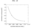
- FIG. 23 is a graph showing a relation between electron injection time and retention threshold voltage decrease amount.
- FIG. 24 is a graph showing a result of fitting data of the diffusion-limited region in the data of FIG. 23 .
- n-type channel memory cell In the embodiments below, descriptions will be given based on an n-type channel memory cell. Also, in the case of a p-type channel memory cell, it can be handled like the n-type channel memory cell. In other words, also in the p-type channel memory cell, hydrogen is released by the hot carrier injection into a silicon nitride film of a charge trapping portion, and the released hydrogen and holes in a silicon substrate cause the NBTI reaction, so that the data retention characteristics are deteriorated.
- a hydrogen concentration represents the total concentration of the N—H bonds and Si—H bonds.
- the hydrogen concentration can be measured by SIMS (Secondary Ion Mass Spectroscopy) or thermal desorption analysis TDS (Thermal Desorption Spectroscopy).
- FIG. 1 is a cross-sectional view of a principal part of a typical nonvolatile semiconductor memory device (flash memory) of the present embodiment.
- a memory cell comprises: an ONO film (ONO) composed of a stacked film of a silicon nitride film (nitride film) SIN being a charge trapping portion, and oxide films (silicon oxide films) BOTOX and TOPOX positioned over and under SIN; a memory gate electrode MG composed of electric conductor such as n-type polysilicon; a source region (source diffusion layer, n-type semiconductor region) MS composed of an n-type impurity (semiconductor region in which the n-type impurity is introduced (silicon region)); and a drain region (drain diffusion layer, n-type semiconductor region) MD composed of an n-type impurity (semiconductor region in which the n-type impurity is introduced (silicon region)).
- ONO film ONO
- nitride film silicon nitride film
- SIN silicon nitride film
- oxide films silicon oxide films
- BOTOX and TOPOX positioned over
- the source region MS and the drain region MD are formed in a p-type well region PWEL provided on a p-type silicon substrate (semiconductor substrate) PSUB.
- a film in which the hydrogen concentration is reduced is used as the silicon nitride film SIN.
- the silicon nitride film SIN a silicon oxynitride film in which the hydrogen concentration is reduced may be used.
- FIG. 2 shows a program operation and an erase operation of the memory cell shown in FIG. 1 .
- the program operation is performed by channel hot electron injection.
- program voltages for example, a voltage applied to the source region MS is 5 V, a voltage applied to the memory gate electrode MG is 7 V, a voltage applied to the drain region MD is 0 V, and a voltage applied to the well is 0 V.
- BTBT Band-To-Band Tunneling
- a voltage applied to the memory gate electrode MG is ⁇ 5 V
- a voltage applied to the source region MS is 6 V
- a voltage applied to the drain region MD is 0 V
- a voltage applied to the well is 0 V.
- a voltage applied to the drain region MD is 1.5 V
- a voltage applied to the source region MS is 0 V
- a voltage applied to the memory gate electrode MG is 1.5 V. The read operation is performed in a manner in which the voltage between the source and drain is in the reverse direction of the program operation.
- an erase method which by applying a negative voltage to the memory gate, electrons are pulled to the silicon substrate with FN tunneling or holes are injected from the substrate with FN tunneling, may be employed. Also, an erase method, which by applying a positive voltage to the memory gate, electrons are pulled to the memory gate with FN tunneling, or holes are injected from the memory gate with FN tunneling, may be employed.
- FIG. 3 shows a relation between the total concentration of N—H bonds and Si—H bonds in the silicon nitride film and the reduction amount of a threshold voltage in data retention for 1000 hours at 150° C. after program/erase cycles have been performed 100 thousand times at a high temperature of 150° C.
- the total concentration of the N—H bonds and Si—H bonds in the silicon nitride film is 2.2 ⁇ 10 21 cm ⁇ 3 when the film is formed by the LPCVD method at 650° C., or is 9 ⁇ 10 20 cm ⁇ 3 by the LPCVD method at an increased temperature of 700° C.
- the hydrogen concentration is 1.1 ⁇ 10 21 cm ⁇ 3 at 630° C.
- the characteristics have no difference. This is because the concentrations are in a region where the rate of the NBTI reaction is limited by the amount of holes, that is, the characteristics are not determined by the amount of hydrogen but by the amount of holes.
- the total concentration of the N—H bonds and the Si—H bonds can be reduced to the first half of the order of 10 20 cm ⁇ 3 .
- the data retention characteristics are improved.
- the total concentration of the N—H bonds and the Si—H bonds is shifted around the first half of the order of 10 20 cm ⁇ 3 by simultaneously introducing a slight amount of NH 3 plasma gas containing hydrogen, the data characteristics are varied depending on the total concentration of the N—H bonds and the Si—H bonds.
- the total concentration of the N—H bonds and the Si—H bonds in the silicon nitride film by which the effect of improving the data retention characteristics is obtained will be derived by another method.
- the hydrogen concentration in the silicon nitride film is reduced by the release of hydrogen with this hot electron injection, and it is confirmed how much the hydrogen concentration has to be reduced to improve the retention characteristics deterioration.
- a memory cell using the silicon nitride film formed at 700° C. by the LPCVD method shown in FIG. 3 is used.
- the test procedure is as described below. First of all, first hot electron injection into the nitride film is performed at a high temperature of 150° C. for t seconds to release the hydrogen in the nitride film, thereby reducing a residual hydrogen concentration of the nitride film. Next, in order to prevent the hydrogen released by the hot electron injection from affecting a retention test to be performed later, sufficient annealing (at 300° C. for 1 hour) for reducing the concentration of the hydrogen which is released to vicinities of the memory cell to which the hot electrons have been injected is performed.
- second hot electron injection is performed at 150° C. to release the hydrogen in the nitride film, and evaluation of the retention characteristics is performed in a next memory cell to which the hot electron injection has not been performed.
- the test are conducted plural times with the first hot electron injection time t being changed in order to derive the residual hydrogen concentration (function of the first hot electron injection time t) of the nitride film at which an effect of suppressing the retention deterioration appears.
- FIG. 23 shows the test result of evaluation of the relation between the first hot electron injection time t and the retention threshold voltage decrease amount.
- the threshold voltage decrease amount substantially does not change until the time of 100 s, and becomes small at 1000 s or more where the effect of suppressing the retention deterioration appears.
- the reason that the threshold voltage decrease amount does not change until 100 s is that the region until 100 s is in the reaction-limited region where the retention deterioration is determined not by the amount of hydrogen but by the amount of holes. It can be understood that the reason the threshold voltage decrease amount becomes small at 1000 s or more is that the region is in the diffusion-limited region where the retention deterioration is determined not by the amount of holes but by the amount of hydrogen.
- the change rate dR(t)/dt of the residual hydrogen concentration R(t) in the nitride film is equivalent to the value of the hydrogen release rate E(t) caused by the hot electron injection when a negative symbol is added to the value.
- R 0 and ⁇ are known, the value thereof can be derived.
- the nitride film used in the present test is the silicon nitride film formed at 700° C. by the LPCVD method.
- the hydrogen concentration R 0 of the film is 9 ⁇ 10 20 cm ⁇ 3 as shown in FIG. 3 .
- a retention threshold voltage decrease amount ⁇ Vth_r(t) shown in FIG. 23 includes components such as discharge of charges to the silicon substrate as well as hydrogen deterioration, and can be expressed as a sum of a decrease component ⁇ Vth_H(t) caused by the hydrogen deterioration and a decrease component ⁇ Vth_e other than the hydrogen deterioration.
- the former deterioration component ⁇ Vth_H(t) caused by the hydrogen deterioration is proportional to the hydrogen release amount caused by the second hot electron injection. It can be said that the hydrogen release amount caused by the second hot electron injection is proportional to the residual hydrogen concentration R(t).
- ⁇ Vth_H(t) and R(t) have a proportional relation.
- the latter decrease component ⁇ Vth_e other than the hydrogen decrease is constant regardless of t. Therefore, the retention threshold voltage decrease amount ⁇ Vth_r(t) is:
- FIG. 24 shows the result of fitting of three points after 1000 at which the retention deterioration is determined by diffusion limited in the measurement data of FIG. 23 .
- the hydrogen concentration in the nitride film which the effect of suppressing retention deterioration caused by decrease of the hydrogen appears, can be estimated to be approximately 6 ⁇ 10 20 /cm 2 , and it was confirmed by the different method that the effect can be obtained when the hydrogen concentration in the nitride film, which the effect of suppressing retention deterioration shown in FIG. 3 appears, is at least 5 ⁇ 10 20 /cm 2 or less.
- FIG. 4 to FIG. 7 are cross-sectional views of principal parts of a substrate showing the manufacturing method of the nonvolatile semiconductor memory device of the present embodiment.
- Memory cells are arranged in an array shape in a memory region; however, a cross sectional part of merely one memory cell is shown in each of the drawings.
- FIG. 4 will be described.
- a cell isolation oxide film region STI is formed, and a p-type well region PWEL which serves as a memory cell region is formed.
- a p-type or n-type impurity region (channel region) ME for adjusting a threshold voltage value is formed.
- an ONO (Oxide Nitride Oxide) film including a silicon nitride film in which a hydrogen concentration (total concentration of N—H bonds and Si—H bonds) is 5 ⁇ 10 20 cm ⁇ 3 or less is stacked.
- a bottom oxide film BOTOX is formed by thermal oxidation or ISSG (In-Situ Steam Generation) oxidation
- a silicon nitride film SIN having a hydrogen concentration of 5 ⁇ 10 20 cm ⁇ 3 or less is formed, and furthermore, a top oxide film TOPOX is formed by vapor phase growth and thermal oxidation or ISSG oxidation.
- film thicknesses of the bottom oxide film BOTOX and the top oxide film TOPOX are desired to be 3 nm or more which does not readily cause a tunneling phenomenon.
- the film thickness of the bottom oxide film BOTOX has to be as thin as approximately 1.5 nm to 3 nm.
- the top oxide film TOPOX is not formed, or the film thickness of the top oxide film TOPOX has to be as thin as 2 nm or less.
- the film thickness of the silicon nitride film SIN made to be 2 nm or more so that electric charges capable of sufficiently shifting the threshold voltage can be trapped.
- the forming method of the silicon nitride film having a low hydrogen concentration will be described later in detail.
- an n-type polysilicon layer NMG (approximately 150 nm) which serves as a memory gate electrode MG is deposited.
- FIG. 5 By using photolithography techniques and dry etching techniques, the n-type polysilicon layer NMG shown in FIG. 4 is processed, thereby forming the memory gate electrode MG.
- the memory gate electrode extends in the depth direction of the drawing and is in a linear pattern.
- the exposed top oxide film TOPOX and the silicon nitride film SIN are respectively removed by hydrofluoric acid and hot phosphoric acid.
- ion implantation of a low-concentration n-type impurity is performed, thereby forming a low-concentration n-type impurity region MDM in a drain part and a low-concentration n-type impurity region MSM in a source part.
- FIG. 6 After the part of the bottom oxide film BOTOX of the ONO film that is exposed from the surface is removed by hydrofluoric acid, an oxide film is deposited, and then is subjected to etching by using anisotropic etching techniques, thereby forming a side wall spacer SW on the side wall of the memory gate electrode MG. Ion implantation of an n-type impurity is performed, thereby forming a drain region MD and a source region MS. Subsequently, a silicon nitride film SACSIN for self align contact (SAC: Self Align Contact) is deposited.
- SAC Self Align Contact
- FIG. 7 An interlayer dielectric film INS 1 is deposited over an entire surface of the silicon substrate.
- a contact hole is formed over the drain region MD, and a metal layer (plug) CONT is formed in the opening (contact hole).
- a first metal line M 1 is formed, and then, an interlayer dielectric film INS 2 is deposited.
- a contact hole is formed in the interlayer dielectric film INS 2 , and an electric conductive film is further deposited and patterned to form a metal line.
- the memory gate electrode MG and the source region MS extend in the direction perpendicular to the paper surface, while the first metal line M 1 which is connected to the drain region MD and serves as a bit line extends in the direction orthogonal to the memory gate electrode MG and the source region MS.
- the source region MS may use the first metal line to extend in the direction parallel to the drain region MD. Furthermore, like the memory cell shown in FIG. 8 , the drain region MD and the source region MS may extend in the direction perpendicular to the paper surface as diffusion layer wiring, and the memory gate electrode MG may extend in the direction orthogonal to the diffusion layer wirings of the drain region MD and the source region MS.
- a manufacturing method of the memory cell shown in FIG. 8 is different from that of the memory cell shown in FIG. 4 to FIG. 7 .
- a bottom oxide film BOTOX of an ONO film, a silicon nitride film SIN of the ONO film, which has a hydrogen concentration of 5 ⁇ 10 20 cm ⁇ 3 or less, and a top oxide film TOPOX of the ONO film are formed.
- the ONO film in a region for formation of a source and a drain is removed by using photolithography techniques and dry etching techniques.
- an oxide film LO is formed by thermal oxidation in the region from which the ONO film is removed, and an n-type impurity is injected thereto to form a drain region MD and a source region MS.
- a polysilicon layer is deposited, and a memory gate electrode MG is formed by photolithography techniques and dry etching techniques.
- the memory gate electrode extends in the horizontal direction of the drawing and is in a linear pattern.
- the ONO film over the source region MS and drain region MD is removed, and the silicon nitride film, which is used as a charge trapping portion, is left merely partially in the memory region.
- a structure in which the entire surface of the memory region is covered with a silicon nitride film, which is used as a charge trapping portion may be used. In this case, except for contact parts, the entire region of the memory region of the memory array is covered with the silicon nitride film.
- the silicon nitride film is a film that does not readily allow permeation of hydrogen, when the entire surface is covered with the silicon nitride film, after formation of the silicon nitride film, hydrogen can be prevented from entering the region of the silicon nitride film serving as a charge trapping portion during manufacturing processes, and therefore, increase of the hydrogen concentration in the silicon nitride film to more than 5 ⁇ 10 20 cm ⁇ 3 can be suppressed.
- the silicon nitride film in FIG. 9 is formed to be shared with a silicon nitrogen film serving as a charge trapping film for other memory cell; an end portion of a side surface of the silicon nitride film is not in the memory cell like FIG. 8 , but formed to be disposed at least outside the memory region; and the silicon nitride film is formed to cover the bottom oxide film.
- the silicon nitride film is formed on the entire surface and covers the entire surface of the bottom oxide film.
- the reason for manufacturing such a structure is described below.
- the hydrogen that is generated during manufacturing processes after formation of the silicon nitride film enters the region of the silicon nitride film serving as a charge trapping portion via the bottom oxide film.
- a main access path of the hydrogen to the bottom oxide film can be a path via a region outside the memory region. Accordingly, covering the entire surface of the bottom oxide film with the silicon nitride film can suppress the phenomenon that hydrogen enters the region of the silicon nitride film serving as the charge trapping portion via the bottom oxide film and the hydrogen concentration in the silicon nitride film is increased to more than 5 ⁇ 10 20 cm ⁇ 3 .
- the bottom oxide film and the silicon nitride film are not formed on the contact parts in the memory region.
- the bottom oxide film is formed on the entire surface in FIG. 9 .
- forming the bottom oxide film on the entire surface is not required for obtaining the effect.
- the bottom oxide film may be partially removed after formation of the bottom oxide film, and the silicon nitride film may be then formed on the entire surface.
- FIG. 1 The embodiments relating to a single gate type memory cell shown in FIG. 1 have been shown. However, the present invention can obtain similar effects in split gate type memory cells shown in cross-sectional views of principal parts of FIG. 10 to FIG. 13 by using a nitride film having a hydrogen concentration of 5 ⁇ 10 20 cm ⁇ 3 or less as a nitride film serving as a charge trapping portion.
- the memory cell shown in FIG. 10 includes: an ONO film composed of a stacked film of a silicon nitride film SIN for trapping charges and oxide films BOTOX and TOPOX positioned over and under the silicon nitride film; a memory gate electrode MG composed of an electric conductor such as n-type polysilicon; a select gate electrode SG composed of n-type polysilicon; a gate dielectric film SGOX positioned under the select gate electrode SG; a source region MS composed of an n-type impurity; and a drain region MD composed of an n-type impurity. Note that the source region MS and the drain region MD are formed in a p-type well region PWEL provided over a p-type silicon substrate PSUB.
- the memory gate electrode MG is formed in the shape of a side wall spacer of the select gate electrode SG. First, the select gate SG is formed, thereafter, the ONO film (BOTOX, SIN, and TOPOX) is formed, and the memory gate electrode MG is formed by utilizing anisotropy etching techniques.
- the select gate SG is formed, thereafter, the ONO film (BOTOX, SIN, and TOPOX) is formed, and the memory gate electrode MG is formed by utilizing anisotropy etching techniques.
- FIG. 11 shows a memory cell in which a select gate electrode SG is formed in the shape of a side wall spacer of a memory gate electrode MG.
- a select gate electrode SG is formed in the shape of a side wall spacer of a memory gate electrode MG.
- an ONO film BOTOX, SIN, and TOPOX
- a side wall spacer GAPSW composed of a dielectric film is formed on the side wall of the memory gate electrode.
- the select gate electrode SG is formed by utilizing anisotropy etching techniques.
- a cap oxide film layer CAP is formed over the memory gate electrode MG.
- FIG. 12 shows a memory cell having a structure in which a memory gate electrode MG partially covers a select gate electrode SG.
- the select gate electrode SG is formed, and then an ONO film and the memory gate electrode MG are formed by utilizing photolithography techniques.
- FIG. 13 shows a memory cell having a structure in which a select gate electrode SG partially covers a memory gate electrode MG.
- the select gate electrode SG is formed by photolithography techniques, it can be formed as well as the memory cell shown in FIG. 11 . In other words, after an ONO film and the memory gate electrode MG are formed, the select gate electrode SG is formed.
- the memory cells shown in FIG. 10 to FIG. 13 can be operated by the same program method, erase method, and read method.
- the point different from the operating methods of the memory cell shown in FIG. 1 is basically merely the program operation.
- the program operation is performed by hot electron injection which is a so-called source side injection method.
- program voltages for example, a voltage Vs applied to the source region MS is 5 V, a voltage Vmg applied to the memory gate electrode MG is 10 V, a voltage Vsg applied to the select gate electrode SG is 1.5 V, a voltage Vd applied to the drain region MD is approximately 0.7 V so that a current flowing into the channel is made to be 1 ⁇ A, and a voltage Vwell applied to the well is 0 V.
- the erase operation is performed by hot hole injection utilizing BTBT or FN tunneling as well as the memory cell shown in FIG. 1 .
- the read operation is also performed by using the voltages between the source and drain applied in a reverse direction to the direction at the time of program as well as the memory cell shown in FIG. 1 .
- the areas of the memory cells are increased; however, the structures have advantages that, for example, the program current can be reduced as compared with the memory cell of FIG. 1 ; a word driver can be configured with a low-voltage MOS transistor by reducing the thickness of the gate dielectric film of the select gate; and a high-speed read operation can be performed.
- the silicon nitride film having a low hydrogen concentration can be formed by any of below manufacturing methods (a) to (c).
- gases of dichlorosilane (SiH 2 Cl 2 ) and ammonia (NH 3 ) are introduced into the furnace at flow rates of 50 sccm and 500 sccm, respectively, so that a silicon nitride film is deposited on the bottom oxide film of the ONO film.
- a film thickness of the silicon nitride film is 1 nm to 8 nm, more preferably, 1 nm to 3 nm.
- a nitrogen gas and an argon gas are ionized by an alternating electric and magnetic field of 13.56 MHz to generate a nitrogen plasma gas
- the silicon nitride film is subjected to plasma nitridation by exposing the nitrogen plasma gas thereto with the LPCD method.
- the substrate temperature is made to be 450° C.
- the hydrogen concentration cannot be readily reduced; therefore, when a thick silicon nitride film is to be formed, preferably deposition of a silicon nitride film by the LPCVD method and plasma nitridation using the nitrogen gas are alternately performed.
- a parallel plate type plasma CVD is employed; however, radical nitraidation using Inductively Coupled Plasma or microwaves can be also performed.
- a silicon nitride film is deposited by a sputtering method using a target material and gas having a small hydrogen content. Since the hydrogen content of the target material and gas is small, the silicon nitride film having a low hydrogen concentration can be formed.
- the substrate temperature is made to be 400° C., and the silicon nitride film is formed by sputtering a target of silicon with an argon and nitrogen gas.
- a silicon nitride film is formed by an ALD method in which the film is alternately exposed to a gas containing silicon but not containing hydrogen and a nitrogen plasma gas. Since hydrogen is not contained in the raw material gases, the silicon nitride film having a low hydrogen concentration is obtained.
- the plasma CVD method not using the ALD method when a thin silicon nitride film is to be formed, the power of plasma generation has to be suppressed, and a silicon nitride film in which silicon is excessive as compared with the composition ratio of Si 3 N 4 is formed.
- the silicon nitride film in which silicon is excessive is inferior in the charge retaining ability since many shallow level traps are present in the film.
- ALD method sufficient nitrogen can be introduced into the silicon nitride film, and therefore the composition ratio of silicon can be reduced until X becomes 0.05 or less in the composition ratio Si 3+X N 4 of silicon and nitrogen.
- the silicon nitride film having a high charge retaining ability can be obtained.
- a charge trapping film having a high charge retaining ability can be formed.
- silicon tetrachloride SiCl 4 is or hexachlorodisilane Si 2 Cl 6 can be used; and as the nitrogen plasma gas, a plasma gas of N 2 or N 2 and a rare gas such as Ar can be used. The plasma gas is generated outside the reactor furnace and introduced thereinto.
- the formation method of the silicon nitride film for charge trapping in which the hydrogen concentration is reduced in the entire film of the silicon nitride film has been described; however, deterioration of the data retention characteristics can be suppressed when the hydrogen concentration in the silicon nitride film can be reduced in the vicinity of the interface between the silicon nitride film and the bottom oxide film or the top oxide film. This is because the hydrogen in the silicon nitride film is not readily diffused, and therefore, among hydrogen that its bonding is broken by the hot carrier injection, hydrogen present at a deep position from the interface of the silicon nitride film cannot escape therefrom.
- the retention temperature is 150° C.
- hydrogen existing in a region that is 3 nm or less from the interface between the silicon nitride film and the bottom oxide film or between the silicon nitride film and the top oxide film deteriorates the data retention characteristics.
- a silicon nitride film SIN 1 having a film thickness of 3 nm or less at the side of the interface with the bottom oxide film is made to be a silicon nitride film having a low hydrogen concentration of 5 ⁇ 10 20 cm ⁇ 3 or less, and also as a silicon nitride film SIN 2 existing over the film SIN 1 , a silicon nitride film is formed by a normally used method such as the LPCVD method, the hydrogen release amount can be reduced. Also, as shown in FIG.
- a silicon nitride film SIN 3 having a film thickness of 3 nm or less at the side of the interface with the top oxide film is made to be a silicon nitride film having a hydrogen concentration of 5 ⁇ 10 20 cm ⁇ 3 or less, in addition to the silicon nitride film SIN 1 having the film thickness of 3 nm or less at the side of the interface with the bottom oxide film, the hydrogen release amount can be further suppressed.
- the thin silicon nitride film SIN 1 or SIN 3 having a low hydrogen concentration can be formed by the above described manufacturing methods (a) to (c).
- the silicon nitride film SIN 1 at the interface side with the bottom oxide film can be formed by a method (d) described below.
- the bottom oxide film BOTOX is subjected to plasma nitridation by a nitrogen plasma gas, so that the oxygen in the bottom oxide film BOTOX is replaced by nitrogen to form a silicon nitride film.
- the oxygen in the bottom oxide film BOTOX is left, so that the silicon nitride film containing oxygen is obtained.
- the hydrogen concentration of the bottom oxide film BOTOX is low, and the gas used in nitridation also does not contain hydrogen; therefore, the silicon nitride film having a low hydrogen concentration can be obtained.
- the silicon nitride film SIN 1 or SIN 3 having a low hydrogen concentration may be formed by combining the above described manufacturing methods (a) to (d).
- a silicon nitride film, for charge trapping, into which the thin film SIN 1 or SIN 3 of the silicon nitride film having a low hydrogen concentration is inserted can be also used in the split gate type memory cells of FIG. 10 to FIG. 13 .
- the data retention characteristics by the hydrogen concentration of 5 ⁇ 10 20 cm ⁇ 3 or less in the nitride film serving as the charge trapping portion has been described above; however, the data retention characteristics can be further improved desirably by using a nitride film having a hydrogen concentration of 3 ⁇ 10 20 cm ⁇ 3 or less, more desirably, a hydrogen concentration of 1 ⁇ 10 20 cm ⁇ 3 or less.
- “diffusion of hydrogen” is controlled, thereby reducing the concentration of released hydrogen and suppressing deterioration of the data retention characteristics.
- the silicon nitride film for SAC on the memory cell is eliminated, thereby ensuring a path through which hydrogen is diffused above the memory cell to reduce the hydrogen concentration in a vicinity of the memory cell.
- SAC techniques are necessary techniques in recent semiconductor devices using MOS transistors, and the silicon nitride film for SAC cannot be eliminated in the entire region of the nonvolatile semiconductor memory device. Therefore, the silicon nitride film for SAC is eliminated merely in the region of a memory array.
- the hydrogen concentration of the nitride film that serves as a charge retention part is not required to be 5 ⁇ 10 20 cm ⁇ 3 or less.
- the hydrogen concentration of the nitride film that serves as the charge retention part is desired to be 5 ⁇ 10 20 cm ⁇ 3 or less.
- FIG. 16 shows cross-sectional views of principal parts of a nonvolatile semiconductor memory device of the present embodiment, and the right and left cross-sectional views respectively show a MONOS type memory cell and a MOS transistor formed in the same semiconductor device.
- the left-side MONOS type memory cell representatively shows one memory cell present in a memory region, and is configured with one MOS transistor. The difference from the memory cell shown in FIG. 7 is that the silicon nitride film SACSIN for SAC is eliminated.
- the right-side transistor representatively shows an n-type or p-type MOS transistor present in the nonvolatile semiconductor memory device, and the case of n-type is shown herein as an example.
- MOS transistors are used in peripheral circuits for operating the nonvolatile semiconductor memory, I/O circuits for inputting/outputting data to or from outside, and logic circuits realizing a microcomputer function in a flash-consolidated microcomputer. In this place, a transistor in a logic region in which a logic circuit is formed is shown. As shown in the right side of FIG. 16 , a silicon nitride film SACSIN for SAC is formed on the MOS transistor.
- FIG. 16 discloses the transistor constituting the memory cell formed in the memory region, the transistor formed in the logic region, a contact connected to the source or drain of the transistor formed in the memory region, and a second contact connected to the source or drain of the transistor of the logic region.
- the gate electrode, the source, and the drain of the transistor of the memory region are not covered with a silicon nitride film for forming a self-align contact.
- the gate electrode, the source and the drain to which the contact of the transistor of the logic region is connected are covered with a silicon nitride film for forming a self-align contact.
- the silicon nitride film for a self-align contact in the logic region is not necessarily required to cover the entire surface, but may be required to be formed at least on the source or drain to which the contact is connected.
- the structure shown in FIG. 16 can be formed by depositing a silicon nitride film for SAC on the entire wafer surface and then selectively removing the silicon nitride film in the memory region by photolithography techniques and etching techniques.
- this structure in a region other than the region of the memory array, circuits in which MOS transistors are disposed with a high density can be manufactured by using SAC techniques; and in the region of the memory array, although there is a drawback that adjustment allowance of contacts has to be secured, deterioration of the data retention characteristics caused by the hydrogen released from the silicon nitride film of the charge trapping portion can be suppressed.
- FIG. 17 shows another mode of the present embodiment.
- all the silicon nitride film for SAC on the memory array is removed; on the other hand, in the embodiment of FIG. 17 , the silicon nitride film for SAC in a vicinity of the contact part of the memory region is left, and the silicon nitride film for SAC on the memory region other than that region is removed.
- This structure can be manufactured by depositing the silicon nitride film for SAC on the entire wafer surface; exposing the region of the silicon nitride film that is desired to be removed by photolithography techniques; and etching the silicon nitride film.
- the silicon nitride film for forming a self-align contact is formed at least on the source or drain to which the contact is connected.
- the silicon nitride film for a self-align contact in the logic region is not always required to cover the entire surface, but is required to be formed at least on the source or drain to which the contact is connected.
- the difference from the example of FIG. 16 is that there is not such a drawback that the adjustment allowance for contact has to be secured. Moreover, since the path through which hydrogen is diffused above the memory cell is ensured, deterioration of the data retention characteristics can be suppressed although the effect is small as compared with the example of FIG. 16 .
- FIG. 16 and FIG. 17 the example using the single gate type memory cell of FIG. 1 has been shown; however, also in the case of using the split gate type memory cells shown in FIG. 10 to FIG. 14 , similar effects can be obtained.
- deterioration reaction caused by hydrogen is suppressed, thereby suppressing deterioration of the data retention characteristics.
- an element such as a halogen element having a larger bonding energy to silicon than hydrogen is introduced into the interface between the silicon substrate and the bottom oxide film and into the bottom oxide film of the memory cell, so that the generation reactions of the interface state and positive fixed charge caused by hydrogen do not readily occur.
- FIG. 18 is a cross-sectional view of a principal part of a nonvolatile semiconductor memory device showing manufacturing processes for realizing the present embodiment, and an example in which an element to be introduced is fluorine which is a halogen element is explained.
- a memory gate electrode MG is formed by using photolithography techniques and dry etching techniques, after the top oxide film TOPOX and the silicon nitride film SIN are respectively removed with hydrofluoric acid and hot phosphoric acid, ion implantation of fluorine is performed.
- the ion implantation amount of fluorine is 2 ⁇ 10 15 cm ⁇ 2 , and the implantation energy is 15 keV.
- fluorine is taken into the interface of the silicon substrate and the bottom oxide film or into the bottom oxide film, and Si—F bonds are formed.
- fluorine other element such as chlorine or deuterium having a larger bonding energy to silicon than hydrogen may be injected. As a result, Si—F bonds are formed in the bottom oxide film.
- FIG. 18 the case of using the single gate type memory cell of FIG. 1 shown in the first embodiment has been shown as an example; however, similar effects can be also obtained in the cases of using the split gate type memory cells shown in FIG. 10 to FIG. 14 .
- the present invention can be applied to nonvolatile semiconductor memory devices.
Landscapes
- Engineering & Computer Science (AREA)
- Microelectronics & Electronic Packaging (AREA)
- Power Engineering (AREA)
- Physics & Mathematics (AREA)
- Condensed Matter Physics & Semiconductors (AREA)
- General Physics & Mathematics (AREA)
- Computer Hardware Design (AREA)
- Ceramic Engineering (AREA)
- Manufacturing & Machinery (AREA)
- Non-Volatile Memory (AREA)
- Semiconductor Memories (AREA)
Applications Claiming Priority (3)
| Application Number | Priority Date | Filing Date | Title |
|---|---|---|---|
| JPJP2007-119122 | 2007-04-27 | ||
| JP2007-119122 | 2007-04-27 | ||
| JP2007119122A JP2008277530A (ja) | 2007-04-27 | 2007-04-27 | 不揮発性半導体記憶装置 |
Publications (2)
| Publication Number | Publication Date |
|---|---|
| US20080265286A1 US20080265286A1 (en) | 2008-10-30 |
| US8063433B2 true US8063433B2 (en) | 2011-11-22 |
Family
ID=39885897
Family Applications (1)
| Application Number | Title | Priority Date | Filing Date |
|---|---|---|---|
| US12/109,340 Expired - Fee Related US8063433B2 (en) | 2007-04-27 | 2008-04-24 | Nonvolatile semiconductor memory device |
Country Status (5)
| Country | Link |
|---|---|
| US (1) | US8063433B2 (zh) |
| JP (1) | JP2008277530A (zh) |
| KR (1) | KR100998106B1 (zh) |
| CN (1) | CN101295735B (zh) |
| TW (1) | TW200908342A (zh) |
Cited By (3)
| Publication number | Priority date | Publication date | Assignee | Title |
|---|---|---|---|---|
| US20130065368A1 (en) * | 2005-06-20 | 2013-03-14 | Renesas Electronics Corporation | Non-volatile semiconductor device and method of fabricating embedded non-volatile semiconductor memory device with sidewall gate |
| US20170018621A1 (en) * | 2013-10-11 | 2017-01-19 | Cypress Semiconductor Corporation | Spacer Formation with Straight Sidewall |
| US11251189B2 (en) | 2009-02-09 | 2022-02-15 | Longitude Flash Memory Solutions Ltd. | Gate fringing effect based channel formation for semiconductor device |
Families Citing this family (10)
| Publication number | Priority date | Publication date | Assignee | Title |
|---|---|---|---|---|
| JP5230274B2 (ja) | 2008-06-02 | 2013-07-10 | 株式会社東芝 | 不揮発性半導体記憶装置 |
| EP2359717B1 (en) | 2008-10-29 | 2014-11-26 | Okamura Corporation | Chair backrest |
| JP2011077323A (ja) * | 2009-09-30 | 2011-04-14 | Tokyo Electron Ltd | 窒化珪素膜の成膜方法および半導体メモリ装置の製造方法 |
| WO2011102233A1 (en) * | 2010-02-19 | 2011-08-25 | Semiconductor Energy Laboratory Co., Ltd. | Semiconductor device |
| US8951864B2 (en) * | 2012-02-13 | 2015-02-10 | Taiwan Semiconductor Manufacturing Company, Ltd. | Split-gate device and method of fabricating the same |
| CN104404476A (zh) * | 2014-12-10 | 2015-03-11 | 中国电子科技集团公司第四十七研究所 | 低压气相淀积Si3N4薄膜的制备方法 |
| TWI548000B (zh) * | 2014-12-22 | 2016-09-01 | 力晶科技股份有限公司 | 半導體元件及其製作方法 |
| JP6890003B2 (ja) * | 2016-11-29 | 2021-06-18 | 株式会社ジャパンディスプレイ | 表示装置 |
| US10304848B2 (en) | 2017-09-01 | 2019-05-28 | Taiwan Semiconductor Manufacturing Co., Ltd. | Flash memory structure with reduced dimension of gate structure |
| JP2021034650A (ja) * | 2019-08-28 | 2021-03-01 | キオクシア株式会社 | 半導体記憶装置 |
Citations (5)
| Publication number | Priority date | Publication date | Assignee | Title |
|---|---|---|---|---|
| US5467309A (en) | 1993-09-06 | 1995-11-14 | Hitachi, Ltd. | Semiconductor nonvolatile memory device having reduced switching overhead time on the program mode |
| US5498890A (en) * | 1989-11-08 | 1996-03-12 | Samsung Electronics Co., Ltd. | Semiconductor device having a multi-layered dielectric structure and manufacturing method thereof |
| JP2002203917A (ja) | 2000-10-26 | 2002-07-19 | Sony Corp | 不揮発性半導体記憶装置およびその製造方法 |
| US20040238878A1 (en) * | 2003-05-30 | 2004-12-02 | Renesas Technology Corp. | Manufacturing method of a semiconductor integrated circuit device |
| US20060065919A1 (en) | 2004-09-29 | 2006-03-30 | Sony Corporation | Nonvolatile memory device and method for producing the same |
Family Cites Families (4)
| Publication number | Priority date | Publication date | Assignee | Title |
|---|---|---|---|---|
| US6794764B1 (en) * | 2003-03-05 | 2004-09-21 | Advanced Micro Devices, Inc. | Charge-trapping memory arrays resistant to damage from contact hole information |
| US6992370B1 (en) * | 2003-09-04 | 2006-01-31 | Advanced Micro Devices, Inc. | Memory cell structure having nitride layer with reduced charge loss and method for fabricating same |
| KR100539158B1 (ko) | 2004-04-20 | 2005-12-26 | 주식회사 하이닉스반도체 | 플래쉬 메모리 소자의 게이트간 유전막 형성 방법 |
| JP2006319082A (ja) * | 2005-05-12 | 2006-11-24 | Sony Corp | 不揮発性半導体メモリデバイス |
-
2007
- 2007-04-27 JP JP2007119122A patent/JP2008277530A/ja active Pending
-
2008
- 2008-03-19 TW TW097109686A patent/TW200908342A/zh unknown
- 2008-04-10 KR KR1020080033183A patent/KR100998106B1/ko not_active IP Right Cessation
- 2008-04-24 US US12/109,340 patent/US8063433B2/en not_active Expired - Fee Related
- 2008-04-25 CN CN2008100953115A patent/CN101295735B/zh not_active Expired - Fee Related
Patent Citations (11)
| Publication number | Priority date | Publication date | Assignee | Title |
|---|---|---|---|---|
| US5498890A (en) * | 1989-11-08 | 1996-03-12 | Samsung Electronics Co., Ltd. | Semiconductor device having a multi-layered dielectric structure and manufacturing method thereof |
| US5467309A (en) | 1993-09-06 | 1995-11-14 | Hitachi, Ltd. | Semiconductor nonvolatile memory device having reduced switching overhead time on the program mode |
| CN1120231A (zh) | 1993-09-06 | 1996-04-10 | 株式会社日立制作所 | 半导体非易失性存储器件 |
| JP2002203917A (ja) | 2000-10-26 | 2002-07-19 | Sony Corp | 不揮発性半導体記憶装置およびその製造方法 |
| US20030122204A1 (en) | 2000-10-26 | 2003-07-03 | Kazumasa Nomoto | Nonvolatile semiconductor storage and method for manufacturing the same |
| US20050230766A1 (en) | 2000-10-26 | 2005-10-20 | Kazumasa Nomoto | Non-volatile semiconductor memory device and method for producing same |
| US20040238878A1 (en) * | 2003-05-30 | 2004-12-02 | Renesas Technology Corp. | Manufacturing method of a semiconductor integrated circuit device |
| KR20040103342A (ko) | 2003-05-30 | 2004-12-08 | 가부시끼가이샤 르네사스 테크놀로지 | 반도체 장치의 제조 방법 및 반도체 장치 |
| JP2004356562A (ja) | 2003-05-30 | 2004-12-16 | Renesas Technology Corp | 半導体装置の製造方法および半導体装置 |
| US20060065919A1 (en) | 2004-09-29 | 2006-03-30 | Sony Corporation | Nonvolatile memory device and method for producing the same |
| JP2006128593A (ja) | 2004-09-29 | 2006-05-18 | Sony Corp | 不揮発性メモリデバイスおよびその製造方法 |
Non-Patent Citations (2)
| Title |
|---|
| H. J. Stein et al., "Chemically Bound hydrogen in CVD Si3/SiH4 Ratio and on Annealing" Journal of the Electrochemical Society, vol. 124, No. 6, pp. 908-912, Jun. 1977. |
| W. M. Arnoldbik et al., "Dynamic behavior of hydrogen in silicon nitride and oxynitride films made by low-pressure chemical vapor deposition" Physical Review B, vol. 48, No. 8, pp. 5444-5456, Aug. 15, 1993. |
Cited By (5)
| Publication number | Priority date | Publication date | Assignee | Title |
|---|---|---|---|---|
| US20130065368A1 (en) * | 2005-06-20 | 2013-03-14 | Renesas Electronics Corporation | Non-volatile semiconductor device and method of fabricating embedded non-volatile semiconductor memory device with sidewall gate |
| US8679915B2 (en) * | 2005-06-20 | 2014-03-25 | Renesas Electronics Corporation | Non-volatile semiconductor device and method of fabricating embedded non-volatile semiconductor memory device with sidewall gate |
| US11251189B2 (en) | 2009-02-09 | 2022-02-15 | Longitude Flash Memory Solutions Ltd. | Gate fringing effect based channel formation for semiconductor device |
| US11950412B2 (en) | 2009-02-09 | 2024-04-02 | Longitude Flash Memory Solutions Ltd. | Gate fringing effect based channel formation for semiconductor device |
| US20170018621A1 (en) * | 2013-10-11 | 2017-01-19 | Cypress Semiconductor Corporation | Spacer Formation with Straight Sidewall |
Also Published As
| Publication number | Publication date |
|---|---|
| JP2008277530A (ja) | 2008-11-13 |
| KR100998106B1 (ko) | 2010-12-02 |
| CN101295735B (zh) | 2010-09-08 |
| TW200908342A (en) | 2009-02-16 |
| KR20080096388A (ko) | 2008-10-30 |
| CN101295735A (zh) | 2008-10-29 |
| US20080265286A1 (en) | 2008-10-30 |
Similar Documents
| Publication | Publication Date | Title |
|---|---|---|
| US8063433B2 (en) | Nonvolatile semiconductor memory device | |
| US9673339B2 (en) | Semiconductor storage device and manufacturing method thereof | |
| US10446656B2 (en) | Memory transistor with multiple charge storing layers and a high work function gate electrode | |
| US7872298B2 (en) | Split-gate type memory device | |
| JP3637332B2 (ja) | 半導体装置及びその製造方法 | |
| US8063434B1 (en) | Memory transistor with multiple charge storing layers and a high work function gate electrode | |
| EP3002780B1 (en) | Method of manufacturing semiconductor device | |
| US8125012B2 (en) | Non-volatile memory device with a silicon nitride charge holding film having an excess of silicon | |
| US11610820B2 (en) | Embedded SONOS and high voltage select gate with a high-K metal gate and manufacturing methods of the same | |
| KR20040093404A (ko) | 반도체장치 및 그 제조방법 | |
| US20040238878A1 (en) | Manufacturing method of a semiconductor integrated circuit device | |
| US20070269972A1 (en) | Method of manufacturing a semiconductor device | |
| US7994012B2 (en) | Semiconductor device and a method of manufacturing the same | |
| US8084315B2 (en) | Method of fabricating non-volatile semiconductor memory device by using plasma film-forming method and plasma nitridation | |
| JP5161494B2 (ja) | 半導体記憶装置 | |
| US6916709B2 (en) | Non-volatile semiconductor memory device and manufacturing method for the same | |
| US8330207B2 (en) | Flash memory device including multilayer tunnel insulator and method of fabricating the same | |
| KR20180119478A (ko) | 반도체 장치 및 반도체 장치의 제조 방법 | |
| US8723248B2 (en) | Nonvolatile semiconductor storage device | |
| KR20080010514A (ko) | 절연막 구조물의 형성 방법 및 이를 이용한 불 휘발성메모리 소자의 형성 방법 | |
| KR20110075395A (ko) | Sonos 구조의 플래시 메모리 소자의 ono막 형성방법 |
Legal Events
| Date | Code | Title | Description |
|---|---|---|---|
| AS | Assignment |
Owner name: RENESAS TECHNOLOGY CORP., JAPAN Free format text: ASSIGNMENT OF ASSIGNORS INTEREST;ASSIGNORS:ISHIMARU, TETSUYA;SHIMAMOTO, YASUHIRO;MINE, TOSHIYUKI;AND OTHERS;REEL/FRAME:020854/0504;SIGNING DATES FROM 20080404 TO 20080407 Owner name: RENESAS TECHNOLOGY CORP., JAPAN Free format text: ASSIGNMENT OF ASSIGNORS INTEREST;ASSIGNORS:ISHIMARU, TETSUYA;SHIMAMOTO, YASUHIRO;MINE, TOSHIYUKI;AND OTHERS;SIGNING DATES FROM 20080404 TO 20080407;REEL/FRAME:020854/0504 |
|
| AS | Assignment |
Owner name: NEC ELECTRRONICS CORPORATION, JAPAN Free format text: MERGER;ASSIGNOR:RENESAS TECHNOLOGY CORP.;REEL/FRAME:024933/0869 Effective date: 20100401 Owner name: RENESAS ELECTRONICS CORPORATION, JAPAN Free format text: CHANGE OF NAME;ASSIGNOR:NEC ELECTRONICS CORPORATION;REEL/FRAME:024953/0404 Effective date: 20100401 |
|
| STCF | Information on status: patent grant |
Free format text: PATENTED CASE |
|
| FEPP | Fee payment procedure |
Free format text: PAYOR NUMBER ASSIGNED (ORIGINAL EVENT CODE: ASPN); ENTITY STATUS OF PATENT OWNER: LARGE ENTITY |
|
| FPAY | Fee payment |
Year of fee payment: 4 |
|
| AS | Assignment |
Owner name: RENESAS ELECTRONICS CORPORATION, JAPAN Free format text: CHANGE OF ADDRESS;ASSIGNOR:RENESAS ELECTRONICS CORPORATION;REEL/FRAME:044928/0001 Effective date: 20150806 |
|
| FEPP | Fee payment procedure |
Free format text: MAINTENANCE FEE REMINDER MAILED (ORIGINAL EVENT CODE: REM.); ENTITY STATUS OF PATENT OWNER: LARGE ENTITY |
|
| LAPS | Lapse for failure to pay maintenance fees |
Free format text: PATENT EXPIRED FOR FAILURE TO PAY MAINTENANCE FEES (ORIGINAL EVENT CODE: EXP.); ENTITY STATUS OF PATENT OWNER: LARGE ENTITY |
|
| STCH | Information on status: patent discontinuation |
Free format text: PATENT EXPIRED DUE TO NONPAYMENT OF MAINTENANCE FEES UNDER 37 CFR 1.362 |
|
| FP | Lapsed due to failure to pay maintenance fee |
Effective date: 20191122 |