US7939188B2 - Magnetic stack design - Google Patents
Magnetic stack design Download PDFInfo
- Publication number
- US7939188B2 US7939188B2 US12/501,632 US50163209A US7939188B2 US 7939188 B2 US7939188 B2 US 7939188B2 US 50163209 A US50163209 A US 50163209A US 7939188 B2 US7939188 B2 US 7939188B2
- Authority
- US
- United States
- Prior art keywords
- layer
- free layer
- free
- pinning
- magnetic stack
- Prior art date
- Legal status (The legal status is an assumption and is not a legal conclusion. Google has not performed a legal analysis and makes no representation as to the accuracy of the status listed.)
- Active, expires
Links
Images


Classifications
-
- G—PHYSICS
- G01—MEASURING; TESTING
- G01R—MEASURING ELECTRIC VARIABLES; MEASURING MAGNETIC VARIABLES
- G01R33/00—Arrangements or instruments for measuring magnetic variables
- G01R33/02—Measuring direction or magnitude of magnetic fields or magnetic flux
- G01R33/06—Measuring direction or magnitude of magnetic fields or magnetic flux using galvano-magnetic devices
- G01R33/09—Magnetoresistive devices
- G01R33/098—Magnetoresistive devices comprising tunnel junctions, e.g. tunnel magnetoresistance sensors
-
- B—PERFORMING OPERATIONS; TRANSPORTING
- B82—NANOTECHNOLOGY
- B82Y—SPECIFIC USES OR APPLICATIONS OF NANOSTRUCTURES; MEASUREMENT OR ANALYSIS OF NANOSTRUCTURES; MANUFACTURE OR TREATMENT OF NANOSTRUCTURES
- B82Y25/00—Nanomagnetism, e.g. magnetoimpedance, anisotropic magnetoresistance, giant magnetoresistance or tunneling magnetoresistance
-
- G—PHYSICS
- G01—MEASURING; TESTING
- G01R—MEASURING ELECTRIC VARIABLES; MEASURING MAGNETIC VARIABLES
- G01R33/00—Arrangements or instruments for measuring magnetic variables
- G01R33/02—Measuring direction or magnitude of magnetic fields or magnetic flux
- G01R33/06—Measuring direction or magnitude of magnetic fields or magnetic flux using galvano-magnetic devices
- G01R33/09—Magnetoresistive devices
- G01R33/093—Magnetoresistive devices using multilayer structures, e.g. giant magnetoresistance sensors
-
- G—PHYSICS
- G11—INFORMATION STORAGE
- G11C—STATIC STORES
- G11C11/00—Digital stores characterised by the use of particular electric or magnetic storage elements; Storage elements therefor
- G11C11/02—Digital stores characterised by the use of particular electric or magnetic storage elements; Storage elements therefor using magnetic elements
- G11C11/16—Digital stores characterised by the use of particular electric or magnetic storage elements; Storage elements therefor using magnetic elements using elements in which the storage effect is based on magnetic spin effect
- G11C11/161—Digital stores characterised by the use of particular electric or magnetic storage elements; Storage elements therefor using magnetic elements using elements in which the storage effect is based on magnetic spin effect details concerning the memory cell structure, e.g. the layers of the ferromagnetic memory cell
-
- H—ELECTRICITY
- H01—ELECTRIC ELEMENTS
- H01F—MAGNETS; INDUCTANCES; TRANSFORMERS; SELECTION OF MATERIALS FOR THEIR MAGNETIC PROPERTIES
- H01F10/00—Thin magnetic films, e.g. of one-domain structure
- H01F10/32—Spin-exchange-coupled multilayers, e.g. nanostructured superlattices
-
- H—ELECTRICITY
- H01—ELECTRIC ELEMENTS
- H01F—MAGNETS; INDUCTANCES; TRANSFORMERS; SELECTION OF MATERIALS FOR THEIR MAGNETIC PROPERTIES
- H01F10/00—Thin magnetic films, e.g. of one-domain structure
- H01F10/32—Spin-exchange-coupled multilayers, e.g. nanostructured superlattices
- H01F10/324—Exchange coupling of magnetic film pairs via a very thin non-magnetic spacer, e.g. by exchange with conduction electrons of the spacer
- H01F10/3254—Exchange coupling of magnetic film pairs via a very thin non-magnetic spacer, e.g. by exchange with conduction electrons of the spacer the spacer being semiconducting or insulating, e.g. for spin tunnel junction [STJ]
-
- H—ELECTRICITY
- H01—ELECTRIC ELEMENTS
- H01F—MAGNETS; INDUCTANCES; TRANSFORMERS; SELECTION OF MATERIALS FOR THEIR MAGNETIC PROPERTIES
- H01F10/00—Thin magnetic films, e.g. of one-domain structure
- H01F10/32—Spin-exchange-coupled multilayers, e.g. nanostructured superlattices
- H01F10/324—Exchange coupling of magnetic film pairs via a very thin non-magnetic spacer, e.g. by exchange with conduction electrons of the spacer
- H01F10/3268—Exchange coupling of magnetic film pairs via a very thin non-magnetic spacer, e.g. by exchange with conduction electrons of the spacer the exchange coupling being asymmetric, e.g. by use of additional pinning, by using antiferromagnetic or ferromagnetic coupling interface, i.e. so-called spin-valve [SV] structure, e.g. NiFe/Cu/NiFe/FeMn
- H01F10/3272—Exchange coupling of magnetic film pairs via a very thin non-magnetic spacer, e.g. by exchange with conduction electrons of the spacer the exchange coupling being asymmetric, e.g. by use of additional pinning, by using antiferromagnetic or ferromagnetic coupling interface, i.e. so-called spin-valve [SV] structure, e.g. NiFe/Cu/NiFe/FeMn by use of anti-parallel coupled [APC] ferromagnetic layers, e.g. artificial ferrimagnets [AFI], artificial [AAF] or synthetic [SAF] anti-ferromagnets
-
- H—ELECTRICITY
- H10—SEMICONDUCTOR DEVICES; ELECTRIC SOLID-STATE DEVICES NOT OTHERWISE PROVIDED FOR
- H10N—ELECTRIC SOLID-STATE DEVICES NOT OTHERWISE PROVIDED FOR
- H10N50/00—Galvanomagnetic devices
- H10N50/10—Magnetoresistive devices
-
- H—ELECTRICITY
- H01—ELECTRIC ELEMENTS
- H01F—MAGNETS; INDUCTANCES; TRANSFORMERS; SELECTION OF MATERIALS FOR THEIR MAGNETIC PROPERTIES
- H01F10/00—Thin magnetic films, e.g. of one-domain structure
- H01F10/32—Spin-exchange-coupled multilayers, e.g. nanostructured superlattices
- H01F10/324—Exchange coupling of magnetic film pairs via a very thin non-magnetic spacer, e.g. by exchange with conduction electrons of the spacer
- H01F10/3286—Spin-exchange coupled multilayers having at least one layer with perpendicular magnetic anisotropy
-
- Y—GENERAL TAGGING OF NEW TECHNOLOGICAL DEVELOPMENTS; GENERAL TAGGING OF CROSS-SECTIONAL TECHNOLOGIES SPANNING OVER SEVERAL SECTIONS OF THE IPC; TECHNICAL SUBJECTS COVERED BY FORMER USPC CROSS-REFERENCE ART COLLECTIONS [XRACs] AND DIGESTS
- Y10—TECHNICAL SUBJECTS COVERED BY FORMER USPC
- Y10T—TECHNICAL SUBJECTS COVERED BY FORMER US CLASSIFICATION
- Y10T428/00—Stock material or miscellaneous articles
- Y10T428/11—Magnetic recording head
- Y10T428/1107—Magnetoresistive
- Y10T428/1114—Magnetoresistive having tunnel junction effect
-
- Y—GENERAL TAGGING OF NEW TECHNOLOGICAL DEVELOPMENTS; GENERAL TAGGING OF CROSS-SECTIONAL TECHNOLOGIES SPANNING OVER SEVERAL SECTIONS OF THE IPC; TECHNICAL SUBJECTS COVERED BY FORMER USPC CROSS-REFERENCE ART COLLECTIONS [XRACs] AND DIGESTS
- Y10—TECHNICAL SUBJECTS COVERED BY FORMER USPC
- Y10T—TECHNICAL SUBJECTS COVERED BY FORMER US CLASSIFICATION
- Y10T428/00—Stock material or miscellaneous articles
- Y10T428/11—Magnetic recording head
- Y10T428/1107—Magnetoresistive
- Y10T428/1143—Magnetoresistive with defined structural feature
Definitions
- Flash memory NAND or NOR
- traditional rotating storage e.g., disc drives
- Resistive sense memories are promising candidates for future nonvolatile and universal memory by storing data bits as either a high or low resistance state.
- MRAM features non-volatility, fast writing/reading speed, almost unlimited programming endurance and zero standby power.
- the basic component of MRAM is a magnetic tunneling junction (MTJ). MRAM switches the MTJ resistance by using a current induced magnetic field to switch the magnetization of MTJ. As the MTJ size shrinks, the switching magnetic field amplitude increases and the switching variation becomes more severe.
- the present disclosure relates to magnetic stacks (e.g., memory cells such as magnetic tunnel junction cells, and read sensors).
- the structures have a pinned reference layer configured for reduced interlayer coupling between the reference layer and the free layer. With these structures, high tunneling magnetoresistance (TMR) can be achieved.
- TMR tunneling magnetoresistance
- this disclosure describes a magnetic stack having a free layer having a switchable magnetization orientation, a reference layer having a pinned magnetization orientation, and a barrier layer therebetween, each of the free layer, reference layer and barrier layer having a center.
- the stack includes an annular antiferromagnetic pinning layer having a center, with the center of the pinning layer aligned with the center of each of the free layer, reference layer and barrier layer, the pinning layer electrically isolated from the free layer and in physical contact with the reference layer.
- this disclosure describes a magnetic stack having a free layer having a switchable magnetization orientation, a reference layer having a pinned magnetization orientation, and a barrier layer therebetween.
- the stack includes an antiferromagnetic pinning layer electrically isolated from the free layer and in physical contact with the reference layer.
- Each of the free layer, reference layer, barrier layer and pinning layer have a center and an outer diameter, with the reference layer having a larger outer diameter than the free layer.
- this disclosure describes a magnetic stack having a free layer having a switchable magnetization orientation, a synthetic antiferromagnetic (SAF) coupled reference layer having a pinned magnetization orientation, and a barrier layer therebetween.
- the SAF reference layer has a first ferromagnetic sublayer and a second ferromagnetic sublayer separated by a metallic spacer, with the first sublayer different than the second sublayer.
- FIG. 1A is a cross-sectional schematic diagram of an illustrative magnetic stack with in-plane magnetization orientation
- FIG. 1B is a cross-sectional schematic diagram of an illustrative perpendicular anisotropy magnetic stack with out-of-plane magnetization orientation
- FIG. 2 is a schematic diagram of an illustrative memory unit including a memory cell and a semiconductor transistor;
- FIG. 3 is a cross-sectional schematic diagram of an embodiment of a magnetic cell
- FIGS. 4A-4J illustrate a stepwise method for forming the magnetic cell of FIG. 3 ;
- FIG. 5 is a cross-sectional schematic diagram of an embodiment of a magnetic cell
- FIG. 6 is a cross-sectional schematic diagram of an embodiment of a magnetic cell
- FIG. 7 is a cross-sectional schematic diagram of an embodiment of a magnetic cell
- FIGS. 8A-8H illustrate a stepwise method for forming the magnetic cell of FIG. 7 ;
- FIG. 9 is a cross-sectional schematic diagram of an embodiment of a magnetic cell.
- This disclosure is directed to magnetic stacks (e.g., spin torque memory (STRAM) cells, RRAM cells, and other resistive sense memory cells (RSM cells) and read sensors).
- the structures have a pinned ferromagnetic reference layer, either a single layer or an SAF trilayer, that is larger than and extends past the ferromagnetic free layer.
- the interlayer coupling between the pinned reference layer and the free layer can be reduced, compared to a cell structure that has the same size for the reference layer and the free layer. Additionally, any electrical shorting issue at the edges of the ferromagnetic layers is inhibited.
- high tunneling magnetoresistance (TMR) can be achieved. High TMR improves readability and writeability of memory arrays incorporated these memory cells.
- the magnetic cells include an annular antiferromagnetic pinning layer that is isolated from the free layer but in physical contact with the reference layer. In other embodiments, the magnetic cells include an asymmetric SAF trilayer.
- FIG. 1A is a cross-sectional schematic diagram of a magnetic cell 10 A that includes a soft ferromagnetic free layer 12 A and a ferromagnetic reference (i.e., pinned) layer 14 A. Ferromagnetic free layer 12 A and ferromagnetic reference layer 14 A are separated by an oxide barrier layer 13 A or non-magnetic tunnel barrier. Note that other layers, such as seed or capping layers, are not depicted for clarity but could be included as technical need arises.
- Reference layer 14 A is larger in size than free layer 12 A and extends past the edges of ferromagnetic free layer 12 A in at least one direction, often in at least two opposite directions.
- each layer e.g., free layer 12 A, reference layer 14 A, etc.
- each layer has a center point and an outer diameter.
- reference layer 14 A has a diameter greater than the diameter of free layer 12 A, so that reference layer 14 A extends past free layer 12 A in all directions.
- Ferromagnetic layers 12 A, 14 A may be made of any useful ferromagnetic (FM) material such as, for example, Fe, Co or Ni and alloys thereof, such as NiFe and CoFe. Ternary alloys, such as CoFeB, may be particularly useful because of their lower moment and high polarization ratio, which are desirable for the spin-current switch.
- Either or both of free layer 12 A and reference layer 14 A may be either a single ferromagnetic layer or a synthetic antiferromagnetic (SAF) coupled structure, i.e., two ferromagnetic sublayers separated by a metallic spacer, such as Ru or Cu, with the magnetization orientations of the sublayers in opposite directions to provide a net magnetization.
- SAF synthetic antiferromagnetic
- the magnetization orientation of ferromagnetic free layer 12 A is more readily switchable than the magnetization orientation of ferromagnetic reference layer 14 A.
- Barrier layer 13 A may be made of an electrically insulating material such as, for example an oxide material (e.g., Al 2 O 3 , TiO x or MgO). Other suitable materials may also be used. Barrier layer 13 A could optionally be patterned with free layer 12 A or with reference layer 14 A, depending on process feasibility and device reliability.
- a first or bottom electrode 18 A is in electrical contact with ferromagnetic reference layer 14 A and a second or top electrode 19 A is in electrical contact with ferromagnetic free layer 12 A. Electrodes 18 A, 19 A electrically connect ferromagnetic layers 12 A, 14 A to a control circuit providing read and write currents through layers 12 A, 14 A.
- isolation layer 16 A Radially encircling at least free layer 12 A, is an isolation layer 16 A, which is electrically insulating.
- isolation layer 16 A encircles free layer 12 A, barrier layer 13 A, and top electrode 19 A.
- Isolation layer 16 A has a thickness of about 2-30 nm and is formed of electrically insulating materials such as oxide(s) and nitride(s). Examples of suitable materials for isolation layer 16 A include Si 3 N 4 , SiO 2 , SiO x N y , SiOCN, Ta 2 O 5 , Al 2 O 3 , MgO, and other low K dielectrics. In other embodiments, isolation layer 16 A encircles free layer 12 A and top electrode 19 A.
- the resistance across magnetic cell 10 A is determined by the relative orientation of the magnetization vectors or magnetization orientations of ferromagnetic layers 12 A, 14 A.
- the magnetization direction of ferromagnetic reference layer 14 A is pinned in a predetermined direction while the magnetization direction of ferromagnetic free layer 12 A is free to rotate under the influence of spin torque.
- Pinning of ferromagnetic reference layer 14 A may be achieved through, e.g., the use of exchange bias with an antiferromagnetically ordered material such as PtMn, IrMn, and others.
- Magnetic memory cell 10 A is in the low resistance state when the magnetization orientation of free layer 12 A is in the same direction (parallel) as the magnetization orientation of reference layer 14 A. Conversely, a magnetic memory cell is in the high resistance state when the magnetization orientation of free layer 12 A is in the opposite direction (anti-parallel) of the magnetization orientation of reference layer 14 A.
- Switching the resistance state and hence the data state of magnetic cell 10 A via spin-transfer occurs when a current, passing through a magnetic layer of magnetic cell 10 A, becomes spin polarized and imparts a spin torque on free layer 12 A.
- a sufficient spin torque is applied to free layer 12 A, the magnetization orientation of free layer 12 A can be switched between two opposite directions and accordingly, magnetic cell 10 A can be switched between the low resistance state and the high resistance state.
- FIG. 1B illustrates an alternate embodiment of a magnetic memory cell that has the magnetization orientations of the free layer and the pinned layer perpendicular to the plane of the layers, or “out-of-plane”.
- magnetic cell 10 B of FIG. 1B has soft ferromagnetic free layer 12 B and a ferromagnetic reference (i.e., pinned) layer 14 B separated by an oxide barrier layer 13 B or non-magnetic tunnel barrier.
- a first or bottom electrode 18 B is in electrical contact with ferromagnetic reference layer 14 B and a second or top electrode 19 B is in electrical contact with ferromagnetic free layer 12 B.
- Electrodes 18 B, 19 B electrically connect ferromagnetic layers 12 B, 14 B to a control circuit providing read and write currents through layers 12 B, 14 B.
- An electrically insulating radial isolation layer 16 B encircles at least free layer 12 A and top electrode 19 B.
- the various elements of cell 10 B are similar to the elements of cell 10 A, described above, except that the magnetization orientations of layers 12 B, 14 B are oriented perpendicular to the layer extension rather than in the layer plane.
- Free layer 12 B and reference layer 14 B each have a magnetization orientation associated therewith, illustrated in FIG. 1B .
- magnetic cell 10 B is in the low resistance state where the magnetization orientation of free layer 12 B is in the same direction (parallel) as the magnetization orientation of reference layer 14 B.
- magnetic cell 10 B is in the high resistance state where the magnetization orientation of free layer 12 B is in the opposite direction (anti-parallel) as the magnetization orientation of reference layer 14 B.
- switching the resistance state and hence the data state of magnetic cell 10 B via spin-transfer occurs when a current, passing through a magnetic layer of magnetic cell 10 B, becomes spin polarized and imparts a spin torque on free layer 12 B.
- a sufficient spin torque is applied to free layer 12 B, the magnetization orientation of free layer 12 B can be switched between two opposite directions and accordingly, magnetic cell 10 B can be switched between the low resistance state and the high resistance state.
- Both memory cells 10 A, 10 B are illustrated with undefined magnetization orientations for free layer 12 A, 12 B.
- a magnetic memory cell is in the low resistance state when the magnetization orientation of free layer 12 A, 12 B is in the same direction as the magnetization orientation of reference layer 14 A, 14 B.
- a magnetic memory cell is in the high resistance state when the magnetization orientation of free layer 12 A, 12 B is in the opposite direction of the magnetization orientation of reference layer 14 A, 14 B.
- the low resistance state is the “0” data state and the high resistance state is the “1” data state, whereas in other embodiments, the low resistance state is “1” and the high resistance state is “0”.
- the magnet stack of memory cells 10 A, 10 B of FIGS. 1A and 1B can also be used as a magnetic read sensor in a hard disc drive with some modifications.
- free layer 12 A, 12 B is influenced by a stored magnetic state on an adjacent recording media, and when a current is passed through the stack, the magnetization orientation in the media can be detected.
- FIG. 2 is a schematic diagram of an illustrative memory unit 20 including a memory element 21 electrically coupled to a semiconductor transistor 22 via an electrically conducting element.
- Memory element 21 may be any of the memory cells described herein.
- Transistor 22 includes a semiconductor substrate 25 having doped regions (e.g., illustrated as n-doped regions) and a channel region (e.g., illustrated as a p-doped channel region) between the doped regions.
- Transistor 22 includes a gate 26 that is electrically coupled to a word line WL to allow selection and current to flow from a source line SL to memory element 21 and bit line BL.
- An array of programmable metallization memory units 20 can be formed on a semiconductor substrate with word lines and bit lines utilizing semiconductor fabrication techniques. Both memory cell 10 A of FIG. 1A and memory cell 10 B of FIG. 1B are illustrated connected to a bit line BL via their top electrode 19 A, 19 B.
- FIG. 3 illustrates a first embodiment of a memory cell having a pinned SAF trilayer reference layer that is larger than and extends past the ferromagnetic free layer.
- This embodiment includes an antiferromagnetic pinning layer that is isolated from the free layer but in physical contact with the reference layer.
- the antiferromagnetic pinning layer is annular in some embodiments.
- memory cell 30 has a soft ferromagnetic free layer 32 and a SAF trilayer reference (i.e., pinned) layer 34 separated by a barrier layer 33 .
- barrier layer 33 is an oxide barrier layer, in other embodiments it can be a non-magnetic tunnel barrier.
- trilayer 34 is composed of two layers of ferromagnetic material (e.g., CoFeB) separated by a layer of Ru, and barrier layer 33 is composed of MgO.
- a first or bottom electrode 38 is in electrical contact with trilayer 34 and a second or top electrode 39 is in electrical contact with ferromagnetic free layer 32 .
- An electrically insulating isolation layer 36 encircles free layer 32 and top electrode 39 .
- the various elements of cell 30 are similar to the element of cells 10 A, 10 B described above, except as noted.
- Memory cell 30 also includes a hard mask 37 positioned above top electrode 39 .
- hard mask 37 is electrically conducting and is integral with or replaces top electrode 39 .
- Memory cell 30 also includes an antiferromagnetic pinning layer 35 radially encircling the stack of barrier layer 33 , free layer 32 and top electrode 39 and electrically insulated therefrom by isolation layer 36 . In the illustrated embodiment, a portion of isolation layer 36 is exposed and not encircled by pinning layer 35 .
- Free layer 32 is physically and electrically isolated from pinning layer 35 , which is in physical contact with trilayer 34 at its extended area (i.e., proximate the outer diameter of trilayer 34 ) and provides pinning for SAF trilayer 34 .
- SAF trilayer 34 is larger than and extends past free layer 32 ; that is, trilayer 34 has a larger outer diameter than free layer 32 .
- Trilayer 34 also is larger than and extends past barrier layer 33 , which in turn is larger than and extends past free layer 32 .
- Trilayer 34 , barrier 33 and free layer 32 are stacked with their centers aligned.
- FIGS. 4A-4J The process flow to make this memory cell stack structure is shown in FIGS. 4A-4J .
- a stack of appropriate materials forming bottom electrode 48 , SAF trilayer 44 , barrier layer 43 , free layer 42 , and top electrode 49 is deposited.
- high-temperature thermal annealing is done to induce the epitaxial formation in barrier layer 43 (e.g., MgO barrier layer) and crystallization of ferromagnetic free layer 42 and SAF trilayer 44 .
- a hard mask 47 is deposited on to top electrode 49 and then patterned.
- free layer 42 is patterned and the etching is stopped at barrier layer 43 .
- a protective layer 46 e.g., silicon nitride, is deposited in FIG. 4C to cover the stack of FIG. 4B . After milling and etching the structure of FIG. 4C , the extended area of SAF trilayer 44 is exposed in FIG. 4D while barrier layer 43 remains covered by protective isolation layer 46 .
- an antiferromagnetic pinning layer 45 is deposited over the structure of FIG. 4D in contact with SAF trilayer 44 at the exposed area.
- a very thin ferromagnetic layer may be deposited over the structure of FIG. 4D before deposition of antiferromagnetic pinning layer 45 to increase the pinning effect.
- milling is performed to trim antiferromagnetic pinning layer 45 to achieve physical, electrical and magnetic separation between hard mask 47 and antiferromagnetic pinning layer 45 .
- pinning layer 45 is an insulator (e.g., NiO)
- this separation is not necessary.
- many pinning materials are metallic and are alloys of Mn, thus the separation is desired.
- the entire stack is annealing at elevated temperature in the presence of a strong external in-plane magnetic field. If Mn is present in pinning layer 45 , this annealing should be within a temperature range so that Mn diffusion is controlled.
- the magnetic field will align the magnetizations of SAF trilayer 44 in the field direction and will also induce exchange bias (pinning) of the top ferromagnetic layer of trilayer 44 (that is in contact with antiferromagnetic pinning layer 45 ).
- the resulting SAF trilayer 44 is pinned by antiferromagnetic layer 45 .
- the memory cell is finalized by deposition of dielectric material 40 in FIG. 4H to encase the structure.
- This dielectric material 40 is polished in FIG. 4I to provide a planar surface, and a bit line BL is deposited and patterned on top electrode 49 and hard mask 47 in FIG. 4J .
- FIG. 5 illustrates another embodiment of a memory cell having a pinned reference layer that is larger than and extends past the ferromagnetic free layer and having an annular pinning layer.
- memory cell 50 has a soft ferromagnetic free layer 52 and a single layer reference (i.e., pinned) layer 54 separated by an oxide barrier layer 53 or non-magnetic tunnel barrier.
- a first or bottom electrode 58 is in electrical contact with reference layer 54 and a second or top electrode 59 is in electrical contact with ferromagnetic free layer 52 .
- a hard mask 57 is positioned above top electrode 59 .
- An electrically insulating radial isolation layer 56 encircles free layer 52 , hard mask 57 and top electrode 59 .
- An antiferromagnetic pinning layer 55 radially encircles at least a portion of isolation layer 56 and the stack of barrier layer 53 , free layer 52 , top electrode 59 and hard mask 57 .
- the various elements of cell 50 are similar to the element of cells 10 A, 10 B, 30 described above, except as noted.
- reference layer 54 is larger than and extends past barrier layer 53 , which in turn is larger than and extends past free layer 52 .
- Reference layer 54 , barrier 53 and free layer 52 are stacked with their centers aligned.
- FIG. 6 illustrates another embodiment of a memory cell having a pinned reference layer that is larger than and extends past the ferromagnetic free layer and that has an asymmetric SAF trilayer instead of a pinning layer.
- memory cell 60 has a soft ferromagnetic free layer 62 and an SAF trilayer reference (i.e., pinned) layer 64 separated by an oxide barrier layer 63 or non-magnetic tunnel barrier.
- a first or bottom electrode 68 is in electrical contact with trilayer 64 and a second or top electrode 69 is in electrical contact with ferromagnetic free layer 62 .
- a hard mask 67 is positioned above top electrode 69 .
- An electrically insulating radial isolation layer 66 encircles free layer 62 , hard mask 67 and top electrode 69 .
- the various elements of cell 60 are similar to the element of cells 10 A, 10 B, 30 , 50 described above, except as noted.
- memory cell 60 has no antiferromagnetic layer for pinning.
- trilayer 64 (composed of a first ferromagnetic layer 64 A, a metallic spacer 64 B, and a second ferromagnetic layer 64 C) is asymmetric in either physical thickness or coercivity between its ferromagnetic layers. That is, ferromagnetic layers 64 A and 64 C either have a different physical thickness or have a different coercivity. In FIG. 6 , layer 64 A is illustrated physically thicker than layer 64 C. The magnetization configuration and orientation of trilayer 64 are defined after magnetic field setting. With no antiferromagnetic pinning layer in cell 60 , trilayer 64 is designed in shape to induce shape anisotropy against thermal activation.
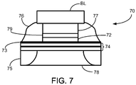
- FIG. 7 illustrates another embodiment of a memory cell having a pinned reference layer that is larger than and extends past the ferromagnetic free layer and having an annular pinning layer.
- memory cell 70 has a soft ferromagnetic free layer 72 and an SAF trilayer reference (i.e., pinned) layer 74 separated by an oxide barrier layer 73 or non-magnetic tunnel barrier.
- a first or bottom electrode 78 is in electrical contact with trilayer 74 and a second or top electrode 79 is in electrical contact with ferromagnetic free layer 72 .
- a hard mask 77 is positioned above top electrode 79 .
- An electrically insulating radial isolation layer 76 encircles free layer 72 , hard mask 77 and top electrode 79 .
- the various elements of cell 70 are similar to the element of cells 10 A, 10 B, 30 , 50 , 60 described above, except as noted.
- Memory cell 70 includes a pinning layer 75 positioned below the stack of free layer 72 , barrier layer 73 , and trilayer 74 .
- pinning layer 75 is an annular ring at the outer periphery of bottom electrode 78 , in physical contact with and exchange coupled with trilayer 74 .
- pinning layer 75 is centered around the stack of free layer 72 , barrier layer 73 , and trilayer 74 and does not vertically overlap or intersect with the stack.
- FIGS. 8A-8H The process flow to make memory cell 70 is shown in FIGS. 8A-8H .
- a metal layer 80 deposited, which will form the eventual bottom electrode.
- Metal layer 80 is masked and patterned (e.g., milled) to form bottom electrode 88 of FIG. 8B .
- antiferromagnetic material is deposited in a ring around bottom electrode 88 and then polished to form pinning layer 85 .
- An SAF trilayer 84 , a barrier layer 83 , a free layer 82 and top electrode 89 are sequentially formed in FIG. 8D over bottom electrode 88 and pinning layer 85 .
- the various layers of pinning layer 85 /bottom electrode 88 , SAF trilayer 84 , barrier layer 83 , free layer 82 and top electrode 89 in the stack have the same diameter.
- free layer 82 and top electrode 89 are masked with hard mask 87 and patterned, to have a reduced size in relation to SAF trilayer 84 and barrier layer 83 .
- Isolation material 86 is deposited in FIG. 8F to cover and encase the structure of FIG. 8E .
- This isolation material 86 is optionally milled and then covered with a dielectric material, which is polished in FIG. 8G to provide a planar surface of hard mask 87 and isolation material 86 .
- a bit line BL is deposited and patterned on top electrode 89 and hard mask 87 in FIG. 8H .
- FIG. 9 An alternate to memory cell 70 of FIG. 7 , with a single pinned reference layer, is shown in FIG. 9 .
- Memory cell 90 of FIG. 9 has a soft ferromagnetic free layer 92 and a single layer reference (i.e., pinned) layer 94 separated by an oxide barrier layer 93 or non-magnetic tunnel barrier.
- a first or bottom electrode 98 is in electrical contact with layer 94 and a second or top electrode 99 is in electrical contact with free layer 92 .
- a hard mask 97 is positioned above top electrode 99 .
- An electrically insulating radial isolation layer 96 encircles free layer 92 , hard mask 97 and top electrode 99 .
- An annular pinning layer 95 is positioned below the stack of free layer 92 , barrier layer 93 , and layer 94 .
- the various elements of cell 90 are similar to the element of cells 10 A, 10 B, 30 , 50 , 60 , 70 described above, except as noted.
- the structures of this disclosure may be made by thin film techniques such as chemical vapor deposition (CVD), physical vapor deposition (PVD), and atomic layer deposition (ALD). Material removal may be by etching, including milling, ion beam milling, wet etching, and the like.
- CVD chemical vapor deposition
- PVD physical vapor deposition
- ALD atomic layer deposition
- Material removal may be by etching, including milling, ion beam milling, wet etching, and the like.
Landscapes
- Engineering & Computer Science (AREA)
- Chemical & Material Sciences (AREA)
- Physics & Mathematics (AREA)
- Crystallography & Structural Chemistry (AREA)
- Power Engineering (AREA)
- Nanotechnology (AREA)
- Condensed Matter Physics & Semiconductors (AREA)
- General Physics & Mathematics (AREA)
- Computer Hardware Design (AREA)
- Mram Or Spin Memory Techniques (AREA)
- Hall/Mr Elements (AREA)
- Magnetic Heads (AREA)
Priority Applications (10)
| Application Number | Priority Date | Filing Date | Title |
|---|---|---|---|
| US12/501,632 US7939188B2 (en) | 2008-10-27 | 2009-07-13 | Magnetic stack design |
| JP2012520671A JP5669839B2 (ja) | 2009-07-13 | 2010-07-08 | 磁気積層体設計 |
| PCT/US2010/041296 WO2011008614A1 (en) | 2009-07-13 | 2010-07-08 | Magnetic stack design |
| KR1020127003810A KR101459511B1 (ko) | 2009-07-13 | 2010-07-08 | 마그네틱 스택 설계 |
| CN201080032381.1A CN102687215B (zh) | 2009-07-13 | 2010-07-08 | 磁性叠层设计 |
| US13/083,693 US8197953B2 (en) | 2008-10-27 | 2011-04-11 | Magnetic stack design |
| JP2013141582A JP5752183B2 (ja) | 2009-07-13 | 2013-07-05 | 磁気積層体設計 |
| JP2013141583A JP2013243378A (ja) | 2009-07-13 | 2013-07-05 | 磁気積層体設計 |
| JP2015075907A JP6113216B2 (ja) | 2009-07-13 | 2015-04-02 | 磁気積層体設計 |
| JP2015134288A JP6193312B2 (ja) | 2009-07-13 | 2015-07-03 | 磁気積層体設計 |
Applications Claiming Priority (2)
| Application Number | Priority Date | Filing Date | Title |
|---|---|---|---|
| US10878708P | 2008-10-27 | 2008-10-27 | |
| US12/501,632 US7939188B2 (en) | 2008-10-27 | 2009-07-13 | Magnetic stack design |
Related Child Applications (1)
| Application Number | Title | Priority Date | Filing Date |
|---|---|---|---|
| US13/083,693 Continuation US8197953B2 (en) | 2008-10-27 | 2011-04-11 | Magnetic stack design |
Publications (2)
| Publication Number | Publication Date |
|---|---|
| US20100102406A1 US20100102406A1 (en) | 2010-04-29 |
| US7939188B2 true US7939188B2 (en) | 2011-05-10 |
Family
ID=42729020
Family Applications (2)
| Application Number | Title | Priority Date | Filing Date |
|---|---|---|---|
| US12/501,632 Active 2029-09-23 US7939188B2 (en) | 2008-10-27 | 2009-07-13 | Magnetic stack design |
| US13/083,693 Expired - Fee Related US8197953B2 (en) | 2008-10-27 | 2011-04-11 | Magnetic stack design |
Family Applications After (1)
| Application Number | Title | Priority Date | Filing Date |
|---|---|---|---|
| US13/083,693 Expired - Fee Related US8197953B2 (en) | 2008-10-27 | 2011-04-11 | Magnetic stack design |
Country Status (5)
| Country | Link |
|---|---|
| US (2) | US7939188B2 (enExample) |
| JP (5) | JP5669839B2 (enExample) |
| KR (1) | KR101459511B1 (enExample) |
| CN (1) | CN102687215B (enExample) |
| WO (1) | WO2011008614A1 (enExample) |
Cited By (8)
| Publication number | Priority date | Publication date | Assignee | Title |
|---|---|---|---|---|
| US20100117169A1 (en) * | 2008-11-11 | 2010-05-13 | Seagate Technology Llc | Memory cell with radial barrier |
| US20110089510A1 (en) * | 2008-08-08 | 2011-04-21 | Seagate Technology Llc | Magnetic memory cell construction |
| US20110180888A1 (en) * | 2008-10-27 | 2011-07-28 | Seagate Technology Llc | Magnetic stack design |
| US20120153413A1 (en) * | 2010-12-20 | 2012-06-21 | Seagate Technology Llc | Non-Volatile Memory Cell with Lateral Pinning |
| US20140346518A1 (en) * | 2010-11-26 | 2014-11-27 | Renesas Electronics Corporation | Magnetic memory including memory cells incorporating data recording layer with perpendicular magnetic anisotropy film |
| US8970991B2 (en) * | 2013-03-12 | 2015-03-03 | Seagate Technology Llc | Coupling feature in a magnetoresistive trilayer lamination |
| US8981503B2 (en) | 2012-03-16 | 2015-03-17 | Headway Technologies, Inc. | STT-MRAM reference layer having substantially reduced stray field and consisting of a single magnetic domain |
| US9614145B2 (en) | 2013-09-03 | 2017-04-04 | Taiwan Semiconductor Manufacturing Co., Ltd. | Reversed stack MTJ |
Families Citing this family (39)
| Publication number | Priority date | Publication date | Assignee | Title |
|---|---|---|---|---|
| JPH0652395B2 (ja) | 1986-08-25 | 1994-07-06 | 富士写真フイルム株式会社 | 写真フイルム用スプ−ル |
| US8169810B2 (en) * | 2008-10-08 | 2012-05-01 | Seagate Technology Llc | Magnetic memory with asymmetric energy barrier |
| US7998758B2 (en) * | 2008-11-05 | 2011-08-16 | Seagate Technology Llc | Method of fabricating a magnetic stack design with decreased substrate stress |
| US8455117B2 (en) * | 2009-03-04 | 2013-06-04 | Seagate Technology Llc | Bit-patterned stack with antiferromagnetic shell |
| JP5492144B2 (ja) * | 2011-05-27 | 2014-05-14 | 株式会社日立製作所 | 垂直磁化磁気抵抗効果素子及び磁気メモリ |
| US9082695B2 (en) * | 2011-06-06 | 2015-07-14 | Avalanche Technology, Inc. | Vialess memory structure and method of manufacturing same |
| US8313959B1 (en) | 2011-08-17 | 2012-11-20 | Taiwan Semiconductor Manufacturing Company, Ltd. | Hole first hardmask definition |
| US9007818B2 (en) | 2012-03-22 | 2015-04-14 | Micron Technology, Inc. | Memory cells, semiconductor device structures, systems including such cells, and methods of fabrication |
| US9368176B2 (en) * | 2012-04-20 | 2016-06-14 | Alexander Mikhailovich Shukh | Scalable magnetoresistive element |
| US9054030B2 (en) | 2012-06-19 | 2015-06-09 | Micron Technology, Inc. | Memory cells, semiconductor device structures, memory systems, and methods of fabrication |
| US8923038B2 (en) | 2012-06-19 | 2014-12-30 | Micron Technology, Inc. | Memory cells, semiconductor device structures, memory systems, and methods of fabrication |
| US9373775B2 (en) | 2012-09-13 | 2016-06-21 | Micron Technology, Inc. | Methods of forming magnetic memory cells |
| US9379315B2 (en) | 2013-03-12 | 2016-06-28 | Micron Technology, Inc. | Memory cells, methods of fabrication, semiconductor device structures, and memory systems |
| US9368714B2 (en) | 2013-07-01 | 2016-06-14 | Micron Technology, Inc. | Memory cells, methods of operation and fabrication, semiconductor device structures, and memory systems |
| US9466787B2 (en) | 2013-07-23 | 2016-10-11 | Micron Technology, Inc. | Memory cells, methods of fabrication, semiconductor device structures, memory systems, and electronic systems |
| US8872149B1 (en) * | 2013-07-30 | 2014-10-28 | Taiwan Semiconductor Manufacturing Company, Ltd. | RRAM structure and process using composite spacer |
| US9203017B2 (en) | 2013-08-02 | 2015-12-01 | Samsung Electronics Co., Ltd. | Method and system for providing magnetic junctions including a package structure usable in spin transfer torque memories |
| US9257636B2 (en) | 2013-09-11 | 2016-02-09 | Taiwan Semiconductor Manufacturing Co., Ltd. | Perpendicular magnetic random-access memory (MRAM) formation by direct self-assembly method |
| US9461242B2 (en) | 2013-09-13 | 2016-10-04 | Micron Technology, Inc. | Magnetic memory cells, methods of fabrication, semiconductor devices, memory systems, and electronic systems |
| US9608197B2 (en) | 2013-09-18 | 2017-03-28 | Micron Technology, Inc. | Memory cells, methods of fabrication, and semiconductor devices |
| US9177576B2 (en) | 2013-10-03 | 2015-11-03 | HGST Netherlands B.V. | Giant magneto resistive sensor and method for making same |
| US10454024B2 (en) | 2014-02-28 | 2019-10-22 | Micron Technology, Inc. | Memory cells, methods of fabrication, and memory devices |
| EP3123476B1 (en) * | 2014-03-28 | 2019-10-16 | Intel Corporation | Techniques for forming spin-transfer-torque memory having a dot-contacted free magnetic layer |
| US9281466B2 (en) | 2014-04-09 | 2016-03-08 | Micron Technology, Inc. | Memory cells, semiconductor structures, semiconductor devices, and methods of fabrication |
| US9269888B2 (en) | 2014-04-18 | 2016-02-23 | Micron Technology, Inc. | Memory cells, methods of fabrication, and semiconductor devices |
| US10003014B2 (en) * | 2014-06-20 | 2018-06-19 | International Business Machines Corporation | Method of forming an on-pitch self-aligned hard mask for contact to a tunnel junction using ion beam etching |
| US9349945B2 (en) | 2014-10-16 | 2016-05-24 | Micron Technology, Inc. | Memory cells, semiconductor devices, and methods of fabrication |
| US9768377B2 (en) | 2014-12-02 | 2017-09-19 | Micron Technology, Inc. | Magnetic cell structures, and methods of fabrication |
| US10439131B2 (en) | 2015-01-15 | 2019-10-08 | Micron Technology, Inc. | Methods of forming semiconductor devices including tunnel barrier materials |
| US9559294B2 (en) | 2015-01-29 | 2017-01-31 | Taiwan Semiconductor Manufacturing Co., Ltd. | Self-aligned magnetoresistive random-access memory (MRAM) structure for process damage minimization |
| US10008662B2 (en) | 2015-03-12 | 2018-06-26 | Taiwan Semiconductor Manufacturing Co., Ltd. | Perpendicular magnetic tunneling junction (MTJ) for improved magnetoresistive random-access memory (MRAM) process |
| KR20170012791A (ko) * | 2015-07-24 | 2017-02-03 | 에스케이하이닉스 주식회사 | 전자 장치의 제조 방법 |
| US9853205B1 (en) * | 2016-10-01 | 2017-12-26 | International Business Machines Corporation | Spin transfer torque magnetic tunnel junction with off-centered current flow |
| WO2019092817A1 (ja) | 2017-11-08 | 2019-05-16 | Tdk株式会社 | トンネル磁気抵抗効果素子、磁気メモリ、及び内蔵型メモリ |
| WO2019092816A1 (ja) | 2017-11-08 | 2019-05-16 | Tdk株式会社 | トンネル磁気抵抗効果素子、磁気メモリ、及び内蔵型メモリ |
| JP2023046271A (ja) * | 2021-09-21 | 2023-04-03 | Tdk株式会社 | 磁気センサ |
| CN115996579B (zh) * | 2021-10-15 | 2026-04-21 | 中国科学院微电子研究所 | 一种sot-mram及其制造方法 |
| US12598918B2 (en) | 2022-05-25 | 2026-04-07 | Tdk Corporation | Magneto-resistive element and method of manufacturing the magneto-resistive element |
| EP4362650B1 (en) * | 2022-10-31 | 2025-08-06 | Commissariat à l'Energie Atomique et aux Energies Alternatives | Magnetic tunnel junction, array of magnetic tunnel junctions, and associated fabrication method |
Citations (26)
| Publication number | Priority date | Publication date | Assignee | Title |
|---|---|---|---|---|
| US6548114B2 (en) | 1998-05-07 | 2003-04-15 | Seagate Technology Llc | Method of fabricating a spin valve/GMR sensor having a synthetic antiferromagnetic layer pinned by Mn-alloy |
| US20040041182A1 (en) | 2002-08-29 | 2004-03-04 | Tuttle Mark E. | MRAM sense layer area control |
| US20040094785A1 (en) * | 2002-11-18 | 2004-05-20 | Xiaochun Zhu | Magentic memory element and memory device including same |
| US6759263B2 (en) | 2002-08-29 | 2004-07-06 | Chentsau Ying | Method of patterning a layer of magnetic material |
| US20040157427A1 (en) | 2003-01-06 | 2004-08-12 | Sony Corporation | Nonvolatile magnetic memory device and manufucturing method thereof |
| US6795279B2 (en) | 2000-04-12 | 2004-09-21 | Seagate Technology Llc | Spin valve structures with specular reflection layers |
| US20050276090A1 (en) | 2004-06-10 | 2005-12-15 | Sony Corporation | Nonvolatile magnetic memory device and photomask |
| US20070008661A1 (en) * | 2004-01-20 | 2007-01-11 | Tai Min | Magnetic tunneling junction film structure with process determined in-plane magnetic anisotropy |
| US7241632B2 (en) | 2005-04-14 | 2007-07-10 | Headway Technologies, Inc. | MTJ read head with sidewall spacers |
| US20070188942A1 (en) * | 2006-02-14 | 2007-08-16 | Beach Robert S | Tunnel MR head with closed-edge laminated free layer |
| US20070187785A1 (en) * | 2006-02-16 | 2007-08-16 | Chien-Chung Hung | Magnetic memory cell and manufacturing method thereof |
| US7307876B2 (en) | 2003-08-19 | 2007-12-11 | New York University | High speed low power annular magnetic devices based on current induced spin-momentum transfer |
| EP1885006A1 (en) | 2006-07-31 | 2008-02-06 | MagIC Technologies Inc. | A novel capping layer for a magnetic tunnel junction device to enhance dR/R and a method of making the same |
| US20080225585A1 (en) * | 2007-02-12 | 2008-09-18 | Yadav Technology | Low Cost Multi-State Magnetic Memory |
| US20080265347A1 (en) * | 2007-04-24 | 2008-10-30 | Iwayama Masayoshi | Magnetoresistive element and manufacturing method thereof |
| US7486552B2 (en) | 2007-05-21 | 2009-02-03 | Grandis, Inc. | Method and system for providing a spin transfer device with improved switching characteristics |
| US20090168506A1 (en) * | 2005-12-31 | 2009-07-02 | Institute Of Physics, Chinese Academy Of Sciences | Close shaped magnetic multi-layer film comprising or not comprising a metal core and the manufacture method and the application of the same |
| US7583529B2 (en) | 2006-10-20 | 2009-09-01 | Industrial Technology Research Institute | Magnetic tunnel junction devices and magnetic random access memory |
| US20090302403A1 (en) | 2008-06-05 | 2009-12-10 | Nguyen Paul P | Spin torque transfer magnetic memory cell |
| US20100033880A1 (en) | 2008-08-08 | 2010-02-11 | Seagate Technology Llc | Multi-bit stram memory cells |
| US20100032777A1 (en) * | 2008-08-08 | 2010-02-11 | Seagate Technology Llc | Magnetic memory cell construction |
| US20100053822A1 (en) * | 2008-08-28 | 2010-03-04 | Seagate Technology Llc | Stram cells with ampere field assisted switching |
| US7688615B2 (en) | 2007-12-04 | 2010-03-30 | Macronix International Co., Ltd. | Magnetic random access memory, manufacturing method and programming method thereof |
| US20100102406A1 (en) * | 2008-10-27 | 2010-04-29 | Seagate Technology Llc | Magnetic stack design |
| US20100109110A1 (en) | 2008-10-30 | 2010-05-06 | Seagate Technology Llc | ST-RAM Cells with Perpendicular Anisotropy |
| US20100117169A1 (en) * | 2008-11-11 | 2010-05-13 | Seagate Technology Llc | Memory cell with radial barrier |
Family Cites Families (14)
| Publication number | Priority date | Publication date | Assignee | Title |
|---|---|---|---|---|
| US5759263A (en) * | 1996-12-05 | 1998-06-02 | Abb Research Ltd. | Device and a method for epitaxially growing objects by cvd |
| JP2001274480A (ja) * | 2000-03-27 | 2001-10-05 | Sharp Corp | 磁気メモリの製造方法 |
| JP2003318460A (ja) * | 2002-04-24 | 2003-11-07 | Alps Electric Co Ltd | 磁気検出素子及びその製造方法 |
| JP2004186659A (ja) * | 2002-10-07 | 2004-07-02 | Alps Electric Co Ltd | 磁気検出素子 |
| JP2004259913A (ja) * | 2003-02-26 | 2004-09-16 | Sony Corp | 環状体の製造方法および磁気記憶装置およびその製造方法 |
| JP2005109201A (ja) * | 2003-09-30 | 2005-04-21 | Fujitsu Ltd | 強磁性トンネル接合素子、磁気メモリセル及び磁気ヘッド |
| JP2005129801A (ja) * | 2003-10-24 | 2005-05-19 | Sony Corp | 磁気記憶素子及び磁気メモリ |
| JP4590862B2 (ja) * | 2003-12-15 | 2010-12-01 | ソニー株式会社 | 磁気メモリ装置及びその製造方法 |
| KR100648143B1 (ko) * | 2004-11-03 | 2006-11-24 | 한국과학기술연구원 | 전류 인가 자기 저항 소자 |
| JP2007053143A (ja) * | 2005-08-15 | 2007-03-01 | Sony Corp | 記憶素子、メモリ |
| CN101000821B (zh) * | 2006-01-11 | 2010-05-12 | 中国科学院物理研究所 | 一种闭合形状的磁性多层膜及其制备方法和用途 |
| JP4384183B2 (ja) * | 2007-01-26 | 2009-12-16 | 株式会社東芝 | 磁気抵抗素子および磁気メモリ |
| JP2008218829A (ja) * | 2007-03-06 | 2008-09-18 | Toshiba Corp | 磁気抵抗素子及びその製造方法 |
| JP2009094104A (ja) * | 2007-10-03 | 2009-04-30 | Toshiba Corp | 磁気抵抗素子 |
-
2009
- 2009-07-13 US US12/501,632 patent/US7939188B2/en active Active
-
2010
- 2010-07-08 CN CN201080032381.1A patent/CN102687215B/zh not_active Expired - Fee Related
- 2010-07-08 WO PCT/US2010/041296 patent/WO2011008614A1/en not_active Ceased
- 2010-07-08 JP JP2012520671A patent/JP5669839B2/ja not_active Expired - Fee Related
- 2010-07-08 KR KR1020127003810A patent/KR101459511B1/ko not_active Expired - Fee Related
-
2011
- 2011-04-11 US US13/083,693 patent/US8197953B2/en not_active Expired - Fee Related
-
2013
- 2013-07-05 JP JP2013141583A patent/JP2013243378A/ja active Pending
- 2013-07-05 JP JP2013141582A patent/JP5752183B2/ja not_active Expired - Fee Related
-
2015
- 2015-04-02 JP JP2015075907A patent/JP6113216B2/ja not_active Expired - Fee Related
- 2015-07-03 JP JP2015134288A patent/JP6193312B2/ja active Active
Patent Citations (26)
| Publication number | Priority date | Publication date | Assignee | Title |
|---|---|---|---|---|
| US6548114B2 (en) | 1998-05-07 | 2003-04-15 | Seagate Technology Llc | Method of fabricating a spin valve/GMR sensor having a synthetic antiferromagnetic layer pinned by Mn-alloy |
| US6795279B2 (en) | 2000-04-12 | 2004-09-21 | Seagate Technology Llc | Spin valve structures with specular reflection layers |
| US20040041182A1 (en) | 2002-08-29 | 2004-03-04 | Tuttle Mark E. | MRAM sense layer area control |
| US6759263B2 (en) | 2002-08-29 | 2004-07-06 | Chentsau Ying | Method of patterning a layer of magnetic material |
| US20040094785A1 (en) * | 2002-11-18 | 2004-05-20 | Xiaochun Zhu | Magentic memory element and memory device including same |
| US20040157427A1 (en) | 2003-01-06 | 2004-08-12 | Sony Corporation | Nonvolatile magnetic memory device and manufucturing method thereof |
| US7307876B2 (en) | 2003-08-19 | 2007-12-11 | New York University | High speed low power annular magnetic devices based on current induced spin-momentum transfer |
| US20070008661A1 (en) * | 2004-01-20 | 2007-01-11 | Tai Min | Magnetic tunneling junction film structure with process determined in-plane magnetic anisotropy |
| US20050276090A1 (en) | 2004-06-10 | 2005-12-15 | Sony Corporation | Nonvolatile magnetic memory device and photomask |
| US7241632B2 (en) | 2005-04-14 | 2007-07-10 | Headway Technologies, Inc. | MTJ read head with sidewall spacers |
| US20090168506A1 (en) * | 2005-12-31 | 2009-07-02 | Institute Of Physics, Chinese Academy Of Sciences | Close shaped magnetic multi-layer film comprising or not comprising a metal core and the manufacture method and the application of the same |
| US20070188942A1 (en) * | 2006-02-14 | 2007-08-16 | Beach Robert S | Tunnel MR head with closed-edge laminated free layer |
| US20070187785A1 (en) * | 2006-02-16 | 2007-08-16 | Chien-Chung Hung | Magnetic memory cell and manufacturing method thereof |
| EP1885006A1 (en) | 2006-07-31 | 2008-02-06 | MagIC Technologies Inc. | A novel capping layer for a magnetic tunnel junction device to enhance dR/R and a method of making the same |
| US7583529B2 (en) | 2006-10-20 | 2009-09-01 | Industrial Technology Research Institute | Magnetic tunnel junction devices and magnetic random access memory |
| US20080225585A1 (en) * | 2007-02-12 | 2008-09-18 | Yadav Technology | Low Cost Multi-State Magnetic Memory |
| US20080265347A1 (en) * | 2007-04-24 | 2008-10-30 | Iwayama Masayoshi | Magnetoresistive element and manufacturing method thereof |
| US7486552B2 (en) | 2007-05-21 | 2009-02-03 | Grandis, Inc. | Method and system for providing a spin transfer device with improved switching characteristics |
| US7688615B2 (en) | 2007-12-04 | 2010-03-30 | Macronix International Co., Ltd. | Magnetic random access memory, manufacturing method and programming method thereof |
| US20090302403A1 (en) | 2008-06-05 | 2009-12-10 | Nguyen Paul P | Spin torque transfer magnetic memory cell |
| US20100033880A1 (en) | 2008-08-08 | 2010-02-11 | Seagate Technology Llc | Multi-bit stram memory cells |
| US20100032777A1 (en) * | 2008-08-08 | 2010-02-11 | Seagate Technology Llc | Magnetic memory cell construction |
| US20100053822A1 (en) * | 2008-08-28 | 2010-03-04 | Seagate Technology Llc | Stram cells with ampere field assisted switching |
| US20100102406A1 (en) * | 2008-10-27 | 2010-04-29 | Seagate Technology Llc | Magnetic stack design |
| US20100109110A1 (en) | 2008-10-30 | 2010-05-06 | Seagate Technology Llc | ST-RAM Cells with Perpendicular Anisotropy |
| US20100117169A1 (en) * | 2008-11-11 | 2010-05-13 | Seagate Technology Llc | Memory cell with radial barrier |
Non-Patent Citations (10)
| Title |
|---|
| Han et al., Nanoring Magnetic Tunnel Junction and Its Application in Magnetic Random Access Memory Demo Devices with Spin-Polarized Current Switching, Journal of Applied Physics, vol. 13, No. 7, Mar. 26, 2008, pp. 7E933-1-7E933-6. |
| Han, X., Wen, Z., Wei, H., J. App. Phys., 103, 07E933-1 to 07E933-6, 2008. * |
| Hayakawa, et al., "Effect of High Annealing Temperature on Giant Tunnel Magnetoresistance Ratio of CoFeB/MgO/CoFeB Magnetic Tunnel Junctions", Applied Physics Letters 89; 232510 (2006). |
| Ikeda, et al., "Giant TMR in CoFeB/MgO/CoFeB Magnetic Tunnel Junctions", Extended Abstracts on the 2007 International Conference on Solid State Devices and Materials, Tsukuba, pp. 746-747 (2007). |
| Kawahara et al., "2Mb Spin-Transfer Torque RAM (SPRAM) with Bit-by-Bit Bidirectional Current Write and Parallelizing-Direction Current Read", 2007 IEEE International Solid State Circuits Conference (2007). |
| Lee et al., "Effect of Electrode Composition on the Tunnel Magnetoresistance of Pseudo-Spin-Valve Magnetic Tunnel Junction with a MgO Tunnel Barrier", Applied Physics Letters 90, 212507 (2007). |
| PCT Search Report and Written Opinion dated Oct. 25, 2010. |
| U.S. Appl. No. 12/200,034, filed Aug. 29, 2008, Inventor: Xi. |
| U.S. Appl. No. 12/233,764, filed Sep. 19, 2008, Inventor: Gao. |
| U.S. Appl. No. 12/268,638, filed Nov. 11, 2008, Inventor: Anderson. |
Cited By (19)
| Publication number | Priority date | Publication date | Assignee | Title |
|---|---|---|---|---|
| US20110089510A1 (en) * | 2008-08-08 | 2011-04-21 | Seagate Technology Llc | Magnetic memory cell construction |
| US20110177621A1 (en) * | 2008-08-08 | 2011-07-21 | Seagate Technology Llc | Magnetic memory cell construction |
| US8287944B2 (en) | 2008-08-08 | 2012-10-16 | Seagate Technology Llc | Magnetic memory cell construction |
| US8288023B2 (en) * | 2008-08-08 | 2012-10-16 | Seagate Technology Llc | Magnetic memory cell construction |
| US8197953B2 (en) * | 2008-10-27 | 2012-06-12 | Seagate Technology Llc | Magnetic stack design |
| US20110180888A1 (en) * | 2008-10-27 | 2011-07-28 | Seagate Technology Llc | Magnetic stack design |
| US8043732B2 (en) * | 2008-11-11 | 2011-10-25 | Seagate Technology Llc | Memory cell with radial barrier |
| US20120061783A1 (en) * | 2008-11-11 | 2012-03-15 | Seagate Technology Llc | Memory cell with radial barrier |
| US20100117169A1 (en) * | 2008-11-11 | 2010-05-13 | Seagate Technology Llc | Memory cell with radial barrier |
| US8440330B2 (en) * | 2008-11-11 | 2013-05-14 | Seagate Technology, Llc | Memory cell with radial barrier |
| US20140346518A1 (en) * | 2010-11-26 | 2014-11-27 | Renesas Electronics Corporation | Magnetic memory including memory cells incorporating data recording layer with perpendicular magnetic anisotropy film |
| US20120153413A1 (en) * | 2010-12-20 | 2012-06-21 | Seagate Technology Llc | Non-Volatile Memory Cell with Lateral Pinning |
| US8541247B2 (en) * | 2010-12-20 | 2013-09-24 | Seagate Technology Llc | Non-volatile memory cell with lateral pinning |
| US8981503B2 (en) | 2012-03-16 | 2015-03-17 | Headway Technologies, Inc. | STT-MRAM reference layer having substantially reduced stray field and consisting of a single magnetic domain |
| US8970991B2 (en) * | 2013-03-12 | 2015-03-03 | Seagate Technology Llc | Coupling feature in a magnetoresistive trilayer lamination |
| US9614145B2 (en) | 2013-09-03 | 2017-04-04 | Taiwan Semiconductor Manufacturing Co., Ltd. | Reversed stack MTJ |
| US10529916B2 (en) | 2013-09-03 | 2020-01-07 | Taiwan Semiconductor Manufacturing Co., Ltd. | Reversed stack MTJ |
| US10840438B2 (en) | 2013-09-03 | 2020-11-17 | Taiwan Semiconductor Manufacturing Co., Ltd. | Reversed stack MTJ |
| US11258007B2 (en) | 2013-09-03 | 2022-02-22 | Taiwan Semiconductor Manufacturing Company, Ltd. | Reversed stack MTJ |
Also Published As
| Publication number | Publication date |
|---|---|
| JP2013243378A (ja) | 2013-12-05 |
| WO2011008614A1 (en) | 2011-01-20 |
| CN102687215B (zh) | 2015-02-11 |
| JP2012533188A (ja) | 2012-12-20 |
| KR20120115205A (ko) | 2012-10-17 |
| US20110180888A1 (en) | 2011-07-28 |
| US8197953B2 (en) | 2012-06-12 |
| JP2015216392A (ja) | 2015-12-03 |
| JP2013254960A (ja) | 2013-12-19 |
| CN102687215A (zh) | 2012-09-19 |
| JP5669839B2 (ja) | 2015-02-18 |
| JP6193312B2 (ja) | 2017-09-06 |
| JP5752183B2 (ja) | 2015-07-22 |
| US20100102406A1 (en) | 2010-04-29 |
| KR101459511B1 (ko) | 2014-11-07 |
| JP2015156501A (ja) | 2015-08-27 |
| JP6113216B2 (ja) | 2017-04-12 |
Similar Documents
| Publication | Publication Date | Title |
|---|---|---|
| US7939188B2 (en) | Magnetic stack design | |
| US8670271B2 (en) | Magnetic stack having assist layers | |
| CN110224058B (zh) | 磁性器件以及对磁性器件的磁性结进行写入的方法 | |
| US8039913B2 (en) | Magnetic stack with laminated layer | |
| US9165625B2 (en) | ST-RAM cells with perpendicular anisotropy | |
| US7999338B2 (en) | Magnetic stack having reference layers with orthogonal magnetization orientation directions | |
| US8217478B2 (en) | Magnetic stack with oxide to reduce switching current | |
| US9461243B2 (en) | STT-MRAM and method of manufacturing the same | |
| EP2656346B1 (en) | Memory array having local source lines | |
| US9741929B2 (en) | Method of making a spin-transfer-torque magnetoresistive random access memory (STT-MRAM) | |
| US20100091564A1 (en) | Magnetic stack having reduced switching current |
Legal Events
| Date | Code | Title | Description |
|---|---|---|---|
| AS | Assignment |
Owner name: SEAGATE TECHNOLOGY LLC,CALIFORNIA Free format text: ASSIGNMENT OF ASSIGNORS INTEREST;ASSIGNORS:XI, HAIWEN;KHOUEIR, ANTOINE;LEE, BRIAN;AND OTHERS;SIGNING DATES FROM 20090602 TO 20090712;REEL/FRAME:022946/0282 Owner name: SEAGATE TECHNOLOGY LLC, CALIFORNIA Free format text: ASSIGNMENT OF ASSIGNORS INTEREST;ASSIGNORS:XI, HAIWEN;KHOUEIR, ANTOINE;LEE, BRIAN;AND OTHERS;SIGNING DATES FROM 20090602 TO 20090712;REEL/FRAME:022946/0282 |
|
| FEPP | Fee payment procedure |
Free format text: PAYOR NUMBER ASSIGNED (ORIGINAL EVENT CODE: ASPN); ENTITY STATUS OF PATENT OWNER: LARGE ENTITY |
|
| AS | Assignment |
Owner name: THE BANK OF NOVA SCOTIA, AS ADMINISTRATIVE AGENT, CANADA Free format text: SECURITY AGREEMENT;ASSIGNOR:SEAGATE TECHNOLOGY LLC;REEL/FRAME:026010/0350 Effective date: 20110118 Owner name: THE BANK OF NOVA SCOTIA, AS ADMINISTRATIVE AGENT, Free format text: SECURITY AGREEMENT;ASSIGNOR:SEAGATE TECHNOLOGY LLC;REEL/FRAME:026010/0350 Effective date: 20110118 |
|
| STCF | Information on status: patent grant |
Free format text: PATENTED CASE |
|
| FPAY | Fee payment |
Year of fee payment: 4 |
|
| FEPP | Fee payment procedure |
Free format text: 7.5 YR SURCHARGE - LATE PMT W/IN 6 MO, LARGE ENTITY (ORIGINAL EVENT CODE: M1555); ENTITY STATUS OF PATENT OWNER: LARGE ENTITY |
|
| MAFP | Maintenance fee payment |
Free format text: PAYMENT OF MAINTENANCE FEE, 8TH YEAR, LARGE ENTITY (ORIGINAL EVENT CODE: M1552); ENTITY STATUS OF PATENT OWNER: LARGE ENTITY Year of fee payment: 8 |
|
| MAFP | Maintenance fee payment |
Free format text: PAYMENT OF MAINTENANCE FEE, 12TH YEAR, LARGE ENTITY (ORIGINAL EVENT CODE: M1553); ENTITY STATUS OF PATENT OWNER: LARGE ENTITY Year of fee payment: 12 |
|
| AS | Assignment |
Owner name: SEAGATE TECHNOLOGY PUBLIC LIMITED COMPANY, CALIFORNIA Free format text: RELEASE BY SECURED PARTY;ASSIGNOR:THE BANK OF NOVA SCOTIA;REEL/FRAME:072193/0001 Effective date: 20250303 Owner name: SEAGATE TECHNOLOGY, CALIFORNIA Free format text: RELEASE BY SECURED PARTY;ASSIGNOR:THE BANK OF NOVA SCOTIA;REEL/FRAME:072193/0001 Effective date: 20250303 Owner name: SEAGATE TECHNOLOGY HDD HOLDINGS, CALIFORNIA Free format text: RELEASE BY SECURED PARTY;ASSIGNOR:THE BANK OF NOVA SCOTIA;REEL/FRAME:072193/0001 Effective date: 20250303 Owner name: I365 INC., CALIFORNIA Free format text: RELEASE BY SECURED PARTY;ASSIGNOR:THE BANK OF NOVA SCOTIA;REEL/FRAME:072193/0001 Effective date: 20250303 Owner name: SEAGATE TECHNOLOGY LLC, CALIFORNIA Free format text: RELEASE BY SECURED PARTY;ASSIGNOR:THE BANK OF NOVA SCOTIA;REEL/FRAME:072193/0001 Effective date: 20250303 Owner name: SEAGATE TECHNOLOGY INTERNATIONAL, CAYMAN ISLANDS Free format text: RELEASE BY SECURED PARTY;ASSIGNOR:THE BANK OF NOVA SCOTIA;REEL/FRAME:072193/0001 Effective date: 20250303 Owner name: SEAGATE HDD CAYMAN, CAYMAN ISLANDS Free format text: RELEASE BY SECURED PARTY;ASSIGNOR:THE BANK OF NOVA SCOTIA;REEL/FRAME:072193/0001 Effective date: 20250303 Owner name: SEAGATE TECHNOLOGY (US) HOLDINGS, INC., CALIFORNIA Free format text: RELEASE BY SECURED PARTY;ASSIGNOR:THE BANK OF NOVA SCOTIA;REEL/FRAME:072193/0001 Effective date: 20250303 Owner name: SEAGATE TECHNOLOGY PUBLIC LIMITED COMPANY, CALIFORNIA Free format text: RELEASE OF SECURITY INTEREST;ASSIGNOR:THE BANK OF NOVA SCOTIA;REEL/FRAME:072193/0001 Effective date: 20250303 Owner name: SEAGATE TECHNOLOGY, CALIFORNIA Free format text: RELEASE OF SECURITY INTEREST;ASSIGNOR:THE BANK OF NOVA SCOTIA;REEL/FRAME:072193/0001 Effective date: 20250303 Owner name: SEAGATE TECHNOLOGY HDD HOLDINGS, CALIFORNIA Free format text: RELEASE OF SECURITY INTEREST;ASSIGNOR:THE BANK OF NOVA SCOTIA;REEL/FRAME:072193/0001 Effective date: 20250303 Owner name: I365 INC., CALIFORNIA Free format text: RELEASE OF SECURITY INTEREST;ASSIGNOR:THE BANK OF NOVA SCOTIA;REEL/FRAME:072193/0001 Effective date: 20250303 Owner name: SEAGATE TECHNOLOGY LLC, CALIFORNIA Free format text: RELEASE OF SECURITY INTEREST;ASSIGNOR:THE BANK OF NOVA SCOTIA;REEL/FRAME:072193/0001 Effective date: 20250303 Owner name: SEAGATE TECHNOLOGY INTERNATIONAL, CAYMAN ISLANDS Free format text: RELEASE OF SECURITY INTEREST;ASSIGNOR:THE BANK OF NOVA SCOTIA;REEL/FRAME:072193/0001 Effective date: 20250303 Owner name: SEAGATE HDD CAYMAN, CAYMAN ISLANDS Free format text: RELEASE OF SECURITY INTEREST;ASSIGNOR:THE BANK OF NOVA SCOTIA;REEL/FRAME:072193/0001 Effective date: 20250303 Owner name: SEAGATE TECHNOLOGY (US) HOLDINGS, INC., CALIFORNIA Free format text: RELEASE OF SECURITY INTEREST;ASSIGNOR:THE BANK OF NOVA SCOTIA;REEL/FRAME:072193/0001 Effective date: 20250303 |