US7790585B2 - Antiferromagnetic half-metallic semiconductor and manufacturing method therefor - Google Patents
Antiferromagnetic half-metallic semiconductor and manufacturing method therefor Download PDFInfo
- Publication number
- US7790585B2 US7790585B2 US11/573,509 US57350905A US7790585B2 US 7790585 B2 US7790585 B2 US 7790585B2 US 57350905 A US57350905 A US 57350905A US 7790585 B2 US7790585 B2 US 7790585B2
- Authority
- US
- United States
- Prior art keywords
- semiconductor
- antiferromagnetic
- states
- state
- density
- Prior art date
- Legal status (The legal status is an assumption and is not a legal conclusion. Google has not performed a legal analysis and makes no representation as to the accuracy of the status listed.)
- Expired - Fee Related, expires
Links
Images




Classifications
-
- C—CHEMISTRY; METALLURGY
- C30—CRYSTAL GROWTH
- C30B—SINGLE-CRYSTAL GROWTH; UNIDIRECTIONAL SOLIDIFICATION OF EUTECTIC MATERIAL OR UNIDIRECTIONAL DEMIXING OF EUTECTOID MATERIAL; REFINING BY ZONE-MELTING OF MATERIAL; PRODUCTION OF A HOMOGENEOUS POLYCRYSTALLINE MATERIAL WITH DEFINED STRUCTURE; SINGLE CRYSTALS OR HOMOGENEOUS POLYCRYSTALLINE MATERIAL WITH DEFINED STRUCTURE; AFTER-TREATMENT OF SINGLE CRYSTALS OR A HOMOGENEOUS POLYCRYSTALLINE MATERIAL WITH DEFINED STRUCTURE; APPARATUS THEREFOR
- C30B29/00—Single crystals or homogeneous polycrystalline material with defined structure characterised by the material or by their shape
- C30B29/10—Inorganic compounds or compositions
- C30B29/46—Sulfur-, selenium- or tellurium-containing compounds
- C30B29/48—AIIBVI compounds wherein A is Zn, Cd or Hg, and B is S, Se or Te
-
- C—CHEMISTRY; METALLURGY
- C30—CRYSTAL GROWTH
- C30B—SINGLE-CRYSTAL GROWTH; UNIDIRECTIONAL SOLIDIFICATION OF EUTECTIC MATERIAL OR UNIDIRECTIONAL DEMIXING OF EUTECTOID MATERIAL; REFINING BY ZONE-MELTING OF MATERIAL; PRODUCTION OF A HOMOGENEOUS POLYCRYSTALLINE MATERIAL WITH DEFINED STRUCTURE; SINGLE CRYSTALS OR HOMOGENEOUS POLYCRYSTALLINE MATERIAL WITH DEFINED STRUCTURE; AFTER-TREATMENT OF SINGLE CRYSTALS OR A HOMOGENEOUS POLYCRYSTALLINE MATERIAL WITH DEFINED STRUCTURE; APPARATUS THEREFOR
- C30B23/00—Single-crystal growth by condensing evaporated or sublimed materials
- C30B23/02—Epitaxial-layer growth
-
- C—CHEMISTRY; METALLURGY
- C30—CRYSTAL GROWTH
- C30B—SINGLE-CRYSTAL GROWTH; UNIDIRECTIONAL SOLIDIFICATION OF EUTECTIC MATERIAL OR UNIDIRECTIONAL DEMIXING OF EUTECTOID MATERIAL; REFINING BY ZONE-MELTING OF MATERIAL; PRODUCTION OF A HOMOGENEOUS POLYCRYSTALLINE MATERIAL WITH DEFINED STRUCTURE; SINGLE CRYSTALS OR HOMOGENEOUS POLYCRYSTALLINE MATERIAL WITH DEFINED STRUCTURE; AFTER-TREATMENT OF SINGLE CRYSTALS OR A HOMOGENEOUS POLYCRYSTALLINE MATERIAL WITH DEFINED STRUCTURE; APPARATUS THEREFOR
- C30B25/00—Single-crystal growth by chemical reaction of reactive gases, e.g. chemical vapour-deposition growth
- C30B25/02—Epitaxial-layer growth
-
- H—ELECTRICITY
- H01—ELECTRIC ELEMENTS
- H01F—MAGNETS; INDUCTANCES; TRANSFORMERS; SELECTION OF MATERIALS FOR THEIR MAGNETIC PROPERTIES
- H01F1/00—Magnets or magnetic bodies characterised by the magnetic materials therefor; Selection of materials for their magnetic properties
- H01F1/0009—Antiferromagnetic materials, i.e. materials exhibiting a Néel transition temperature
-
- H—ELECTRICITY
- H01—ELECTRIC ELEMENTS
- H01F—MAGNETS; INDUCTANCES; TRANSFORMERS; SELECTION OF MATERIALS FOR THEIR MAGNETIC PROPERTIES
- H01F1/00—Magnets or magnetic bodies characterised by the magnetic materials therefor; Selection of materials for their magnetic properties
- H01F1/01—Magnets or magnetic bodies characterised by the magnetic materials therefor; Selection of materials for their magnetic properties of inorganic materials
- H01F1/40—Magnets or magnetic bodies characterised by the magnetic materials therefor; Selection of materials for their magnetic properties of inorganic materials of magnetic semiconductor materials, e.g. CdCr2S4
- H01F1/401—Magnets or magnetic bodies characterised by the magnetic materials therefor; Selection of materials for their magnetic properties of inorganic materials of magnetic semiconductor materials, e.g. CdCr2S4 diluted
- H01F1/402—Magnets or magnetic bodies characterised by the magnetic materials therefor; Selection of materials for their magnetic properties of inorganic materials of magnetic semiconductor materials, e.g. CdCr2S4 diluted of II-VI type, e.g. Zn1-x Crx Se
-
- H—ELECTRICITY
- H01—ELECTRIC ELEMENTS
- H01F—MAGNETS; INDUCTANCES; TRANSFORMERS; SELECTION OF MATERIALS FOR THEIR MAGNETIC PROPERTIES
- H01F1/00—Magnets or magnetic bodies characterised by the magnetic materials therefor; Selection of materials for their magnetic properties
- H01F1/01—Magnets or magnetic bodies characterised by the magnetic materials therefor; Selection of materials for their magnetic properties of inorganic materials
- H01F1/40—Magnets or magnetic bodies characterised by the magnetic materials therefor; Selection of materials for their magnetic properties of inorganic materials of magnetic semiconductor materials, e.g. CdCr2S4
- H01F1/401—Magnets or magnetic bodies characterised by the magnetic materials therefor; Selection of materials for their magnetic properties of inorganic materials of magnetic semiconductor materials, e.g. CdCr2S4 diluted
- H01F1/404—Magnets or magnetic bodies characterised by the magnetic materials therefor; Selection of materials for their magnetic properties of inorganic materials of magnetic semiconductor materials, e.g. CdCr2S4 diluted of III-V type, e.g. In1-x Mnx As
-
- H—ELECTRICITY
- H01—ELECTRIC ELEMENTS
- H01F—MAGNETS; INDUCTANCES; TRANSFORMERS; SELECTION OF MATERIALS FOR THEIR MAGNETIC PROPERTIES
- H01F1/00—Magnets or magnetic bodies characterised by the magnetic materials therefor; Selection of materials for their magnetic properties
- H01F1/01—Magnets or magnetic bodies characterised by the magnetic materials therefor; Selection of materials for their magnetic properties of inorganic materials
- H01F1/40—Magnets or magnetic bodies characterised by the magnetic materials therefor; Selection of materials for their magnetic properties of inorganic materials of magnetic semiconductor materials, e.g. CdCr2S4
- H01F1/408—Magnets or magnetic bodies characterised by the magnetic materials therefor; Selection of materials for their magnetic properties of inorganic materials of magnetic semiconductor materials, e.g. CdCr2S4 half-metallic, i.e. having only one electronic spin direction at the Fermi level, e.g. CrO2, Heusler alloys
-
- H—ELECTRICITY
- H10—SEMICONDUCTOR DEVICES; ELECTRIC SOLID-STATE DEVICES NOT OTHERWISE PROVIDED FOR
- H10D—INORGANIC ELECTRIC SEMICONDUCTOR DEVICES
- H10D62/00—Semiconductor bodies, or regions thereof, of devices having potential barriers
- H10D62/80—Semiconductor bodies, or regions thereof, of devices having potential barriers characterised by the materials
Definitions
- the present invention relates to an antiferromagnetic half-metallic semiconductor, and a manufacturing method therefor, which is antiferromagnetic and half-metallic, which shows metallic properties in one of up and down electronic spin states, but shows insulating or semiconducting properties in the other electronic spin state.
- a ferromagnetic half-metallic magnet Conventionally known as a ferromagnetic half-metallic magnet (hereinafter referred to as a half-metallic ferromagnet) are Heusler alloys, perovskite-type manganese oxides, zinc-blend-type CrAs, diluted magnetic semiconductors, etc. Semiconductor materials using electron charges and spins, namely spintronics materials, have been studied in recent years. Spintronics materials include zinc-blend-type CrAs and diluted magnetic semiconductors. Known as a diluted magnetic semiconductor are, for example, (In, Mn)As and (Ga, Mn)As.
- the half-metallic antiferromagnet proposed by Picket is a transition metal oxide based intermetallic compound, but not a semiconductor based spintronics material. In fact, no one has manufactured or proposed a half-metallic antiferromagnet as a spintronics material.
- an object of the present invention is to provide an antiferromagnetic half-metallic semiconductor, and a manufacturing method therefor, which is a new antiferromagnetic and half-metallic spintronics material.
- An antiferromagnetic half-metallic semiconductor of the present invention is manufactured by adding to a semiconductor two or more types of magnetic elements including a magnetic element with a d-electron number of less than five and a magnetic element with a d-electron number of more than five, and substituting a part of elements of the semiconductor with the two or more types of magnetic elements.
- a d-electron number of one magnetic element is the same or approximately the same as a positive hole number of the other magnetic element.
- the two types of magnetic elements are any one combination selected from the group of Ti and Ni, V and Co, Cr and Fe, Ti and Fe, Ti and Co, V and Fe, V and Ni, Cr and Co, Cr and Ni, Fe and Co, Mn and Fe, Mn and Co, V and Mn, and Cr and Mn.
- Mn has a d-electron number of less than five or more than five, depending on the host semiconductor or a magnetic element combined therewith.
- the two types of magnetic elements are V and Co.
- FIG. 22 and FIG. 23 show density-of-states curves of V and Co in the case of V and Co with parallel magnetic moments, and density-of-states curves after coupling of V and Co, respectively.
- FIG. 24 and FIG. 25 show density-of-states curves of V and Co in the case of V and Co with antiparallel magnetic moments, and density-of-states curves after coupling of V and Co, respectively.
- a longitudinal axis represents a magnitude of energy, with a curve to the left of the longitudinal axis representing a density of states of up spin electrons, and a right curve a density of states of down spin electrons. Hatching of oblique lines in the drawings represents that d-orbitals contain electrons.
- FIG. 23 shows curves representing a density of states of the up spin electrons and down spin electrons after coupling. At this time, the electron energy is slightly decreased as a whole. This implies that the ferromagnetic coupling of V and Co with parallel magnetic moments is stabilized with the electron energy being decreased due to superexchange interaction.
- FIG. 25 shows curves representing a density of states of the up spin electrons and down spin electrons after coupling. At this time, the electron energy is decreased as a whole. This implies that the antiferromagnetic coupling of V and Co with antiparallel magnetic moments is stabilized with the electron energy being decreased due to double exchange interaction.
- both the up spin electrons and down spin electrons of V and Co move between v and Co, so that the density of states of the up spin electrons and down spin electrons will be represented by the curves shown in FIG. 23 as described above.
- both of the up spin electrons and down spin electrons have a density of states more than zero near the Fermi energy E F , so that half-metallicity will probably not be exhibited.
- the down spin electrons In contrast, in the case of V and Co with antiparallel magnetic moments as shown in FIG. 24 , the down spin electrons hardly move between V and Co because the energy difference between the down spin electrons of V and Co is great. Only the up spin electrons move between V and Co, so that the density of states of the up spin electrons and down spin electrons will be represented by the curves shown in FIG. 25 as described above. As illustrated, the down spin electrons have a density of states of zero to form a band gap Gp. The Fermi energy E F is present in the band gap. On the other hand, the up spin electrons have a density of states greater than zero near the Fermi energy E F , so that half-metallicity will probably be exhibited.
- Antiferromagnetism is exhibited as described above if the d-electron number of one of two types of magnetic elements is the same as the positive hole number of the other magnetic element. If the d-electron number of one magnetic element and the positive hole number of the other magnetic element are not completely the same but approximately the same, ferrimagnetism having slight magnetism as a whole is probably exhibited because the two types of magnetic elements have slightly different magnitudes of magnetic moments. In the present specification, “antiferromagnetism” includes “ferrimagnetism” having slight magnetism.
- three types of magnetic elements are add, wherein a total d-electron number of any two types of magnetic elements is the same or approximately the same as a positive hole number of one type of magnetic element other than the two types of magnetic elements.
- the three types of magnetic elements are any one combination selected from the group of Ti, V, and Ni, Ti, V, and Co, Ti, Ni, and Co, V, Ni, and Co, Cr, Mn, and Co, and V, Mn, and Fe.
- two of the three types of magnetic elements are ferromagnetically coupled with their magnetic moments being parallel, and the two types of magnetic elements and the other one type of magnetic element are antiferromagnetically coupled with their magnetic moments being antiparallel.
- a total d-electron number of the two types of magnetic elements is the same or the approximately same as a positive hole number of the one type of magnetic element other than the two types of magnetic elements. Therefore, antiferromagnetism is exhibited as in the first specific configuration where two types of magnetic elements are added.
- Ti and V are ferromagnetically coupled, while Ni is antiferromagnetically coupled with Ti and V.
- Ti, V, and Co Ti and V are ferromagnetically coupled, while Co is antiferromagnetically coupled with Ti and V.
- Ni, and Co Ni and Co are ferromagnetically coupled, while Co is antiferromagnetically coupled with Ti and Ni.
- V, Ni, and Co Ni and Co are ferromagnetically coupled, while V is antiferromagnetically coupled with Ni and Co.
- the three types of magnetic elements are Cr, Mn, and Co, then Co and Mn are ferromagnetically coupled, while Cr is antiferromagnetically coupled with Co and Mn. If the three types of magnetic elements are V, Mn, and Fe, then V and Mn are ferromagnetically coupled, while Fe is antiferromagnetically coupled with V and Mn.
- the antiferromagnetic half-metallic semiconductor and manufacturing method therefor of the present invention can realize a new antiferromagnetic and half-metallic spintronics material.
- FIG. 1 is a graph showing electronic densities of states of a semiconductor represented by a composition formula (Zn 0.9 Cr 0.05 Fe 0.05 )S in an antiferromagnetic state;
- FIG. 2 is a graph showing electronic densities of states of the above semiconductor in a ferromagnetic state
- FIG. 3 is a graph showing electronic densities of states of the above semiconductor in a spin glass state
- FIG. 4 is a graph showing a relationship between a concentration of Cr and Fe and an antiferromagnetic transition temperature
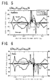
- FIG. 5 is a graph showing electronic densities of states of a semiconductor represented by a composition formula (Zn 0.09 V 0.05 Co 0.05 )S in an antiferromagnetic state;
- FIG. 6 is a graph showing electronic densities of states of the above semiconductor in a ferromagnetic state
- FIG. 7 is a graph showing electronic densities of states of the above semiconductor in a spin glass state
- FIG. 8 is a graph showing electronic densities of states of a semiconductor represented by a composition formula (Zn 0.9 Cr 0.05 Co 0.05 )O in an antiferromagnetic state;
- FIG. 9 is a graph showing electronic densities of states of the above semiconductor in a spin glass state
- FIG. 10 is a graph showing electronic densities of states of a semiconductor represented by a composition formula (Zn 0.9 Cr 0.05 Fe 0.05 )Se in an antiferromagnetic state;
- FIG. 11 is a graph showing electronic densities of states of the above semiconductor in a spin glass state
- FIG. 12 is a graph showing electronic densities of states of a semiconductor represented by a composition formula Zn 0.9 Cr 0.05 Fe 0.05 )O in an antiferromagnetic state;
- FIG. 13 is a graph showing electronic densities of states of a semiconductor represented by a composition formula Cu(Al 0.9 V 0.05 Mn 0.05 )S 2 in an antiferromagnetic state;
- FIG. 14 is a graph showing electronic densities of states of the above semiconductor in a ferromagnetic state
- FIG. 15 is a graph showing electronic densities of states of the above semiconductor in a spin glass state
- FIG. 16 is a graph showing electronic densities of states of a semiconductor represented by a composition formula (Zn 0.9 Cr 0.05 Mn 0.025 Co 0.025 )S in an antiferromagnetic state;
- FIG. 17 is a graph showing electronic densities of states of the above semiconductor in a ferromagnetic state
- FIG. 18 is a graph showing electronic densities of states of the above semiconductor in a spin glass state
- FIG. 19 is a graph showing electronic densities of states of a semiconductor represented by a composition formula (Ti 0.9 Mn 0.05 Co 0.05 )O 2 in an antiferromagnetic state;
- FIG. 20 is a graph showing electronic densities of states of a semiconductor represented by a composition formula (Ti 0.9 Fe 0.05 Co 0.05 )O 2 in an antiferromagnetic state;
- FIG. 21 is a graph showing electronic densities of states of a semiconductor represented by a composition formula (Ti 0.9 Cr 0.05 Co 0.05 )O 2 in an antiferromagnetic state;
- FIG. 22 illustrates density-of-states curves of V and Co in the case of V and Co with parallel magnetic moments
- FIG. 23 illustrates density-of-states curves after coupling of V and Co in the above case
- FIG. 24 illustrates density-of-states curves of V and Co in the case of V and Co with antiparallel magnetic moments
- FIG. 25 illustrates density-of-states curves after coupling of V and Co in the above case.
- An antiferromagnetic half-metallic semiconductor of the present invention has a part of elements of the semiconductor substituted with two or more types of magnetic elements including a magnetic element with a d-electron number of less than five and a magnetic element with a d-electron number of more than five.
- the antiferromagnetic half-metallic semiconductor of the present invention is manufactured by growing a host semiconductor thin film on a substrate, and simultaneously adding several % each of two or more types of magnetic elements including a magnetic element with a d-electron number of less than five and a magnetic element with a d-electron number of more than five.
- Examples of the host semiconductor to be employed include II-VI compound semiconductors, III-V compound semiconductors, I-III-VI compound semiconductors having a chalcopyrite-type crystal structure, II-IV-V compound semiconductors having a chalcopyrite-type crystal structure, and oxide semiconductors.
- Examples of a II-VI compound semiconductor to be employed may include ZnO, ZnSe, ZnS, ZnTe, and CdTe.
- Examples of a III-V compound semiconductor to be employed may include GaAs, GaN, InAs, AlAs, InSb, GaSb, GaP, and InP.
- Examples of a chalcopyrite-type I-III-VI compound semiconductor to be employed may include CuAlS 2 , AgCaS 2 , and AgGaS 2 .
- Examples of a chalcopyrite-type II-IV-V compound semiconductor to be employed may include CdGeP 2 , ZnGeP 2 , and CdGeAs 2 .
- an example of an oxide semiconductor to be employed may include TiO 2 .
- Known thin film growth methods may be employed including an MBE (Molecular Beam Epitaxy) method, a laser MBE method, a low-temperature MBE method, and an MOCVD (Metal Organic Chemical Vapour Deposition) method. It is desirable to employ a low-temperature MBE method if a III-V compound semiconductor is grown as a semiconductor thin film on a substrate.
- MBE Molecular Beam Epitaxy
- laser MBE method a laser MBE method
- MOCVD Metal Organic Chemical Vapour Deposition
- the magnetic elements to be added are two types of transition metal elements, and a d-electron number of one magnetic element is the same or approximately the same as a positive hole number of the other magnetic element.
- the two types of transition metal elements are one combination selected from the group of, for example, Ti and Ni, V and Co, Cr and Fe, Ti and Fe, Ti and Co, V and Fe, V and Ni, Cr and Co, Cr and Ni, Fe and Co, Mn and Fe, Mn and Co, V and Mn, and Cr and Mn.
- Three types of transition metal elements may also be used.
- the three types of transition metal elements are one combination selected from the group of, for example, Ti, V, and Ni, Ti, V, and Co, Ti, Ni, and Co, V, Ni, and Co, Cr, Mn, and Co, and V, Mn, and Fe.
- a II-VI compound semiconductor thin film is grown as a semiconductor thin film, then a II element is substituted with the magnetic elements. If a III-V compound semiconductor thin film is grown, then a III element is substituted with the magnetic elements. If a chalcopyrite-type I-III-VI compound semiconductor thin film is grown, then a III element is substituted with the magnetic elements. If a chalcopyrite-type II-IV-V compound semiconductor is grown, then a II element is substituted with the magnetic elements.
- the down spin electrons hardly move between V and Co because the energy difference between the down spin electrons of V and Co is great.
- the up spin electrons move between V and Co, so that the density of states of the up spin electrons and down spin electrons will be represented by curves shown in FIG. 25 .
- the down spin electrons have a density of states of zero to form a band gap Gp.
- the Fermi energy E F is present in the band gap.
- the up spin electrons have a density of states more than zero near the Fermi energy E F , so that half-metallicity will probably be exhibited.
- Antiferromagnetism is exhibited as described above if the d-electron number of one of two types of magnetic elements is the same as the positive hole number of the other magnetic element. If the d-electron number of one magnetic element and the positive hole number of the other magnetic element are not completely the same but approximately the same, ferrimagnetism having slight magnetism as a whole is probably exhibited because the two types of magnetic elements have slightly different magnitudes of magnetic moments. For example, (Zn 0.9 Cr 0.05 Co 0.05 )S is ferromagnetic, but can be antiferromagnetic by being adjusted in concentrations of Cr and Co.
- the three types of transition metal elements are adjusted in concentration such that a total d-electron number of any two of the three types of transition metal elements is the same or approximately the same as a positive hole number of one type of magnetic element other than the two types of magnetic elements to thereby provide an antiferromagnetic semiconductor.
- concentration such that a total d-electron number of any two of the three types of transition metal elements is the same or approximately the same as a positive hole number of one type of magnetic element other than the two types of magnetic elements to thereby provide an antiferromagnetic semiconductor.
- (Zn 0.9 Cr 0.05 Mn 0.025 Co 0.025 )S is made antiferromagnetic by adding 5% of Cr and 2.5% each of Mn and Co to ZnS to equalize the total d-electron number of Mn and Co to the positive hole number of Cr.
- (Zn 0.9 V 0.025 Mn 0.025 Fe 0.05 )S is made antiferromagnetic by adding 5% of Fe and 2.5% each of Mn and V to ZnS to equalize the total d-electron number of Mn and Fe to the positive hole number of V.
- the antiferromagnetic half-metallic semiconductor of the present invention is antiferromagnetic and insensitive to external magnetic fields, and therefore expected to be applied to different devices from those of ferromagnetic spintronics materials, which are sensitive to external magnetic fields.
- MRAMs Magnetic Random Access Memory
- sensors spin injection devices, magneto-optical devices, spin transistors, spin FETS, single-spin superconductors, etc.
- the antiferromagnetic half-metallic semiconductor of the present invention is half-metallic, and therefore can provide a high switching speed when applied to a semiconductor switching device.
- a diluted antiferromagnetic half-metallic semiconductor of the present embodiment is represented by a composition formula (Zn 0.9 Cr 0.05 Fe 0.05 )S, and has a part of a II element Zn of a II-VI compound semiconductor of ZnS substituted with transition metal elements of Cr and Fe.
- a manufacturing method for the diluted antiferromagnetic half-metallic semiconductor includes growing a ZnS thin film on a GaAs(100) substrate with a laser MBE method, and simultaneously irradiating Cr gas and Fe gas toward the substrate to add 5% each of Cr and Fe.
- the substrate temperature is set, for example, to 150-200° C., with a Zn molecular beam having a beam pressure of, for example, 2.5 ⁇ 10 ⁇ 5 to 8 ⁇ 10 ⁇ 5 Pa, and an S molecular beam having a beam pressure of, for example, 1.5 ⁇ 10 ⁇ 4 to 12 ⁇ 10 ⁇ 4 Pa.
- the gas pressure of Cr and Fe is set, for example, to 2.5 ⁇ 10 ⁇ 6 to 15 ⁇ 10 ⁇ 6 Pa.
- the present inventors performed first-principles electronic state calculations in order to confirm that the above manufacturing method exhibits half-metallicity and antiferromagnetism.
- a method of the first-principles electronic state calculations employed here is a known KKR-CPA-LDA method, which is a combination of the KKR (Korringa-Kohn-Rostoker) method (also called the Green function method), the CPA (Coherent-Potential Approximation) method, and the LDA (Local-Density Approximation) method.
- FIG. 1 through FIG. 3 show density-of-states curves in an antiferromagnetic state, a ferromagnetic state, and a spin glass state with disordered local magnetic moment directions, respectively, obtained by the first-principles electronic state calculations.
- solid lines represent a total density of states
- one-dot chain lines a local density of states of Cr at a 3 d orbital position
- broken lines a local density of states of Fe at a 3 d orbital position.
- FIG. 3 shows only density-of-states curves of up spin electrons in the spin glass state. Density-of-states curves of down spin electrons are the same as those of the up spin electrons, and therefore not shown.
- the down spin electrons In the antiferromagnetic state, as indicated by solid lines in FIG. 1 , the down spin electrons have a density of states of zero to form a band gap Gp. The Fermi energy is present in the band gap. On the other hand, the up spin electrons have a density of states greater than zero near the Fermi energy. Thus, the down spin electron state represents semiconducting properties, while the up spin electron state represents metallic properties, so that it can be said that half-metallicity is exhibited.
- both the up spin electrons and down spin electrons have a density of states greater than zero near the Fermi energy, so that it can be said that half-metallicity is not exhibited.
- the up spin electrons have a density of states grater than zero near the Fermi energy.
- the down spin electrons also have a density of states grater than zero near the Fermi energy, so that it can be said that half-metallicity is not exhibited.
- an antiferromagnetic transition temperature (Neel temperature) at which an antiferromagnetic state changes to a paramagnetic state was calculated to be 445 K.
- the antiferromagnetic transition temperature was calculated with mean field approximation from an energy difference between the spin glass state and antiferromagnetic state, as in a known method for calculating a ferromagnetic transition temperature (Curie temperature) at which a ferromagnetic state changes to a paramagnetic state.
- FIG. 4 shows a calculation result of the antiferromagnetic transition temperature.
- Plots in the drawing represent calculation values of the antiferromagnetic transition temperature when x in a composition formula represented as (Zn 1-x Cr x/2 Fe x/2 )S is 0.02, 0.04, 0.06, 0.08, or 0.10.
- the curve is an approximate curve connecting these plots.
- the diluted antiferromagnetic half-metallic semiconductor of the present embodiment has an antiferromagnetic transition temperature (445 K) higher than room temperature, and therefore can be used in devices that operate at room temperature or more.
- a diluted antiferromagnetic half-metallic semiconductor of the present embodiment is represented by a composition formula (Zn 0.9 V 0.05 Co 0.05 )S, and has a part of a II element Zn of a II-VI compound semiconductor of ZnS substituted with transition metal elements of v and Co.
- a manufacturing method for the diluted antiferromagnetic half-metallic semiconductor includes growing a ZnS thin film on a GaAs(100) substrate with a laser MBE method, and simultaneously adding 5% each of V and Co.
- the present inventors performed first-principles electronic state calculations, as in the first embodiment, in order to confirm that the above manufacturing method exhibits half-metallicity and antiferromagnetism.
- FIG. 5 through FIG. 7 show density-of-states curves in an antiferromagnetic state, a ferromagnetic state and a spin glass state, respectively, obtained by the first-principles electronic state calculations.
- solid lines represent a total density of states
- one-dot chain lines a local density of states of V at a 3 d orbital position
- broken lines a local density of states of Co at a 3 d orbital position.
- FIG. 7 shows only density-of-states curves of up spin electrons in the spin glass state. Density-of-states curves of down spin electrons are the same as those of the up spin electrons, and therefore not shown.
- the down spin electrons In the antiferromagnetic state, as indicated by solid lines in FIG. 5 , the down spin electrons have a density of states of zero to form a band gap Gp. The Fermi energy is present in the band gap. On the other hand, the up spin electrons have a density of states greater than zero near the Fermi energy. Thus, it can be said that half-metallicity is exhibited.
- both the up spin electrons and down spin electrons have a density of states greater than zero near the Fermi energy, so that it can be said that half-metallicity is not exhibited.
- the up spin electrons have a density of states grater than zero near the Fermi energy.
- the down spin electrons also have a density of states grater than zero near the Fermi energy, so that it can be said that half-metallicity is not exhibited.
- an antiferromagnetic transition temperature was calculated to be 349 K.
- the diluted antiferromagnetic half-metallic semiconductor of the present embodiment has an antiferromagnetic transition temperature higher than room temperature, and therefore can be used in devices that operate at room temperature or more.
- a diluted antiferromagnetic half-metallic semiconductor of the present embodiment is represented by a composition formula (Zn 0.9 Cr 0.05 Co 0.05 )O, and has a part of a II element Zn of a II-VI compound semiconductor of ZnO substituted with transition metal elements of Cr and Co.
- a manufacturing method for the diluted antiferromagnetic half-metallic semiconductor includes growing a ZnO thin film on a GaAs(100) substrate with a laser MBE method, and simultaneously adding 5% each of Cr and Co.
- the present inventors performed first-principles electronic state calculations, as in the first embodiment, in order to confirm that the above manufacturing method exhibits half-metallicity and antiferromagnetism.
- FIG. 8 and FIG. 9 show density-of-states curves in an antiferromagnetic state and a spin glass state, respectively, obtained by the first-principles electronic state calculations.
- solid lines represent a total density of states
- one-dot chain lines a local density of states of Cr at a 3 d orbital position
- broken lines a local density of states of Co at a 3 orbital position.
- FIG. 9 shows only density-of-states curves of up spin electrons in the spin glass state. Density-of-states curves of down spin electrons are the same as those of the up spin electrons, and therefore not shown.
- the down spin electrons In the antiferromagnetic state, as indicated by solid lines in FIG. 8 , the down spin electrons have a density of states of zero to form a band gap Gp. The Fermi energy is present in the band gap. On the other hand, the up spin electrons have a density of states greater than zero near the Fermi energy. Thus, it can be said that half-metallicity is exhibited.
- the up spin electrons have a density of states grater than zero near the Fermi energy.
- the down spin electrons also have a density of states grater than zero near the Fermi energy, so that it can be said that half-metallicity is not exhibited. It has been confirmed that half-metallicity is not exhibited also in the ferromagnetic state.
- the antiferromagnetic state is the most stable to exhibit antiferromagnetism.
- an antiferromagnetic transition temperature was calculated to be 484 K.
- the diluted antiferromagnetic half-metallic semiconductor of the present embodiment has an antiferromagnetic transition temperature higher than room temperature, and therefore can be used in devices that operate at room temperature or more.
- a diluted antiferromagnetic half-metallic semiconductor of the present embodiment is represented by a composition formula (Zn 0.9 Cr 0.05 Fe 0.05 )Se, and has a part of a II element Zn of a II-VI compound semiconductor of ZnSe substituted with transition metal elements of Cr and Fe.
- a manufacturing method for the diluted antiferromagnetic half-metallic semiconductor includes growing a ZnSe thin film on a GaAs(100) substrate with a laser MBE method, and simultaneously adding 5% each of Cr and Fe.
- the present inventors performed first-principles electronic state calculations, as in the first embodiment, in order to confirm that the above manufacturing method exhibits half-metallicity and antiferromagnetism.
- FIG. 10 and FIG. 11 show density-of-states curves in an antiferromagnetic state and a spin glass state, respectively, obtained by the first-principles electronic state calculations.
- solid lines represent a total density of states
- one-dot chain lines a local density of states of Cr at a 3 d orbital position
- broken lines a local density of states of Fe at a 3 d orbital position.
- FIG. 11 shows only density-of-states curves of up spin electrons in the spin glass state. Density-of-states curves of down spin electrons are the same as those of the up spin electrons, and therefore not shown.
- the down spin electrons In the antiferromagnetic state, as indicated by solid lines in FIG. 10 , the down spin electrons have a density of states of zero to form a band gap Gp. The Fermi energy is present in the band gap. On the other hand, the up spin electrons have a density of states greater than zero near the Fermi energy. Thus, it can be said that half-metallicity is exhibited.
- the up spin electrons have a density of states grater than zero near the Fermi energy.
- the down spin electrons also have a density of states grater than zero near the Fermi energy, so that it can be said that half-metallicity is not exhibited. It has been confirmed that half-metallicity is not exhibited also in the ferromagnetic state.
- the antiferromagnetic state is the most stable to exhibit antiferromagnetism.
- an antiferromagnetic transition temperature was calculated to be 315 K.
- the diluted antiferromagnetic half-metallic semiconductor of the present embodiment has an antiferromagnetic transition temperature higher than room temperature, and therefore can be used in devices that operate at room temperature or more.
- a diluted antiferromagnetic half-metallic semiconductor of the present embodiment is represented by a composition formula (Zn 0.9 Cr 0.05 Fe 0.05 )O, and has a part of a II element Zn of a II-VI compound semiconductor of ZnO substituted with transition metal elements of Cr and Fe.
- a manufacturing method for the diluted antiferromagnetic half-metallic semiconductor includes growing a ZnO thin film on a GaAs(100) substrate with a laser MBE method, and simultaneously adding 5% each of Cr and Fe.
- the present inventors performed first-principles electronic state calculations, as in the first embodiment, in order to confirm that the above manufacturing method exhibits half-metallicity and antiferromagnetism.
- FIG. 12 shows density-of-states curves in an antiferromagnetic state obtained by the first-principles electronic state calculations.
- solid lines represent a total density of states
- one-dot chain lines a local density of states of Cr at a 3 d orbital position
- broken lines a local density of states of Fe at a 3 d orbital position.
- the up spin electrons have a density of states of zero to form a band gap Gp.
- the Fermi energy is present in the band gap.
- the down spin electrons have a density of states greater than zero near the Fermi energy.
- half-metallicity is exhibited. It has been confirmed that half-metallicity is not exhibited in the ferromagnetic state and spin glass state.
- the antiferromagnetic state is the most stable to exhibit antiferromagnetism.
- a diluted antiferromagnetic half-metallic semiconductor of the present embodiment is represented by a composition formula Cu(Al 0.9 V 0.05 Mn 0.05 )S 2 , and has a part of a III element Al of a I-III-VI compound semiconductor of CuAlS 2 substituted with transition metal elements of V and Mn.
- a manufacturing method for the diluted antiferromagnetic half-metallic semiconductor includes growing a CuAlS 2 thin film on a GaAs(100) substrate with a laser MBE method, and simultaneously adding 5% each of V and Mn.
- the present inventors performed first-principles electronic state calculations, as in the first embodiment, in order to confirm that the above manufacturing method exhibits half-metallicity and antiferromagnetism.
- FIG. 13 through FIG. 15 show density-of-states curves in an antiferromagnetic state, a ferromagnetic state and a spin glass state, respectively, obtained by the first-principles electronic state calculations.
- solid lines represent a total density of states
- one-dot chain lines a local density of states of V at a 3 d orbital position
- broken lines a local density of states of Mn at a 3 d orbital position.
- FIG. 15 shows only density-of-states curves of up spin electrons in the spin glass state. Density-of-states curves of down spin electrons are the same as those of the up spin electrons, and therefore not shown.
- the up spin electrons In the antiferromagnetic state, as indicated by solid lines in FIG. 13 , the up spin electrons have a density of states of zero to form a band gap Gp. The Fermi energy is present in the band gap. On the other hand, the down spin electrons have a density of states greater than zero near the Fermi energy. Thus, it can be said that half-metallicity is exhibited.
- the down spin electrons In the ferromagnetic state, as indicated by solid lines in FIG. 14 , the down spin electrons have a density of states of zero to form a band gap Gp. The Fermi energy is present in the band gap. On the other hand, the up spin electrons have a density of states greater than zero near the Fermi energy. Thus, it can be said that half-metallicity is exhibited.
- the up spin electrons have a density of states grater than zero near the Fermi energy.
- the down spin electrons also have a density of states grater than zero near the Fermi energy, so that it can be said that half-metallicity is not exhibited.
- the antiferromagnetic state is the most stable to exhibit antiferromagnetism.
- the present inventors have confirmed with first-principles electronic state calculations that an antiferromagnetic half-metallic semiconductor can be obtained also by adding to AgGaS 2 two types of magnetic elements of Mn and Fe, or two types of magnetic elements of Mn and Co. They also have confirmed with first-principles electronic state calculations that an antiferromagnetic half-metallic semiconductor can be obtained also by adding to CuAlS 2 two types of magnetic elements of Cr and Mn, or two types of magnetic elements of Mn and Fe.
- a diluted antiferromagnetic half-metallic semiconductor of the present embodiment is represented by a composition formula (Zn 0.09 Cr 0.05 Mn 0.025 Co 0.025 )S, and has a part of a II element Zn of a II-VI compound semiconductor of ZnS substituted with transition metal elements of Cr, Mn, and Co.
- a manufacturing method for the diluted antiferromagnetic half-metallic semiconductor includes growing a znS thin film on a GaAs(100) substrate with a laser MBE method, and simultaneously adding 5% of Cr and 2.5% each of Mn and Co.
- the present inventors performed first-principles electronic state calculations, as in the first embodiment, in order to confirm that the above manufacturing method exhibits half-metallicity and antiferromagnetism.
- FIG. 16 through FIG. 18 show density-of-states curves in an antiferromagnetic state, a ferromagnetic state and a spin glass state, respectively, obtained by the first-principles electronic state calculations.
- solid lines represent a total density of states
- one-dot chain lines a local density of states of Cr at a 3 d orbital position
- broken lines a local density of states of Mn at a 3 d orbital position
- two-dot chain lines a local density of states of Co at a 3 d orbital position.
- FIG. 18 shows only density-of-states curves of up spin electrons in the spin glass state. Density-of-states curves of down spin electrons are the same as those of the up spin electrons, and therefore not shown.
- the down spin electrons In the antiferromagnetic state, as indicated by solid lines in FIG. 16 , the down spin electrons have a density of states of zero to form a band gap Gp. The Fermi energy is present in the band gap. On the other hand, the up spin electrons have a density of states greater than zero near the Fermi energy. Thus, it can be said that half-metallicity is exhibited.
- both the up spin electrons and down spin electrons have a density of states greater than zero near the Fermi energy, so that it can be said that half-metallicity is not exhibited.
- the up spin electrons have a density of states grater than zero near the Fermi energy.
- the down spin electrons also have a density of states grater than zero near the Fermi energy, so that it can be said that half-metallicity is not exhibited.
- the antiferromagnetic state is the most stable to exhibit antiferromagnetism.
- the present inventors have confirmed with first-principles electronic state calculations that an antiferromagnetic half-metallic semiconductor can be obtained also by adding to ZnS three types of magnetic elements of V, Mn and Fe.
- a diluted antiferromagnetic half-metallic semiconductor of the present embodiment is represented by a composition formula (Ti 0.9 Mn 0.05 Co 0.05 )O 2 , and has a part of an element Ti of an oxide semiconductor of TiO 2 substituted with transition metal elements of Mn and Co.
- TiO 2 has a rutile-type crystal structure.
- a manufacturing method for the diluted antiferromagnetic half-metallic semiconductor includes growing a TiO 2 thin film on a GaAs(100) substrate with a laser MBE method, and simultaneously adding 5% each of Mn and Co.
- the present inventors performed first-principles electronic state calculations, as in the first embodiment, in order to confirm that the above manufacturing method exhibits half-metallicity and antiferromagnetism.
- FIG. 19 shows density-of-states curves in an antiferromagnetic state obtained by the first-principles electronic state calculations.
- thicker solid lines represent a total density of states
- one-dot chain lines a local density of states of Mn at a 3 d orbital position
- thinner solid lines a local density of states of Co at a 3 d orbital position.
- the down spin electrons have a density of states of zero to form a band gap Gp.
- the Fermi energy is present in the band gap.
- the up spin electrons have a density of states greater than zero near the Fermi energy. Thus, it can be said that half-metallicity is exhibited.
- the antiferromagnetic state is the most stable to exhibit antiferromagnetism.
- an antiferromagnetic half-metallic semiconductor can be obtained also by adding to TiO 2 two types of magnetic elements of Fe and Co, or two types of magnetic elements of Cr and Co.
- FIG. 20 shows density-of-states curves in an antiferromagnetic state obtained by first-principles electronic state calculations for a semiconductor represented by a composition formula (Ti 0.9 Fe 0.05 Co 0.05 )O 2 .
- thicker solid lines represent a total density of states
- one-dot chain lines a local density of states of Mn at a 3 d orbital position
- thinner solid lines a local density of states of Co at a 3 d orbital position.
- the down spin electrons have a density of states of zero to form a band gap Gp.
- the Fermi energy is present in the band gap.
- the up spin electrons have a density of states greater than zero near the Fermi energy. Thus, it can be said that half-metallicity is exhibited.
- FIG. 21 shows density-of-states curves in an antiferromagnetic state obtained by first-principles electronic state calculations for a semiconductor represented by a composition formula (Ti 0.9 Cr 0.05 Co 0.05 )O 2 .
- thicker solid lines represent a total density of states
- dotted lines a local density of states of Cr at a 3 d orbital position
- thinner solid lines a local density of states of Co at a 3 d orbital position.
- the down spin electrons have a density of states of zero to form a band gap Gp.
- the Fermi energy is present in the band gap.
- the up spin electrons have a density of states greater than zero near the Fermi energy. Thus, it can be said that half-metallicity is exhibited.
- FIG. 19 through FIG. 21 show the calculation result in the case of adding two types of magnetic elements to a rutile-type TiO 2 .
- a rutile-type TiO 2 and an anatase-type TiO 2 have approximately the same electronic state. Therefore, it can be said that an antiferromagnetic half-metallic semiconductor can be obtained by adding two types of magnetic elements to an anatase-type TiO 2 .
Landscapes
- Chemical & Material Sciences (AREA)
- Engineering & Computer Science (AREA)
- Power Engineering (AREA)
- Organic Chemistry (AREA)
- Crystallography & Structural Chemistry (AREA)
- Materials Engineering (AREA)
- Metallurgy (AREA)
- Inorganic Chemistry (AREA)
- Chemical Kinetics & Catalysis (AREA)
- General Chemical & Material Sciences (AREA)
- Hall/Mr Elements (AREA)
- Hard Magnetic Materials (AREA)
- Thin Magnetic Films (AREA)
Applications Claiming Priority (3)
| Application Number | Priority Date | Filing Date | Title |
|---|---|---|---|
| JP2004263479 | 2004-09-10 | ||
| JP2004-263479 | 2004-09-10 | ||
| PCT/JP2005/017100 WO2006028299A1 (ja) | 2004-09-10 | 2005-09-09 | 反強磁性ハーフメタリック半導体及びその製造方法 |
Publications (2)
| Publication Number | Publication Date |
|---|---|
| US20090224340A1 US20090224340A1 (en) | 2009-09-10 |
| US7790585B2 true US7790585B2 (en) | 2010-09-07 |
Family
ID=36036563
Family Applications (1)
| Application Number | Title | Priority Date | Filing Date |
|---|---|---|---|
| US11/573,509 Expired - Fee Related US7790585B2 (en) | 2004-09-10 | 2005-09-09 | Antiferromagnetic half-metallic semiconductor and manufacturing method therefor |
Country Status (4)
| Country | Link |
|---|---|
| US (1) | US7790585B2 (ja) |
| EP (1) | EP1788589A4 (ja) |
| JP (1) | JPWO2006028299A1 (ja) |
| WO (1) | WO2006028299A1 (ja) |
Cited By (1)
| Publication number | Priority date | Publication date | Assignee | Title |
|---|---|---|---|---|
| US20110017938A1 (en) * | 2008-03-21 | 2011-01-27 | Osaka University | Half-metallic antiferromagnetic material |
Families Citing this family (4)
| Publication number | Priority date | Publication date | Assignee | Title |
|---|---|---|---|---|
| JP2010073882A (ja) * | 2008-09-18 | 2010-04-02 | Osaka Univ | 磁気抵抗効果膜、及びこれを具えた磁気抵抗効果素子、並びに磁気デバイス |
| JP2011066334A (ja) * | 2009-09-18 | 2011-03-31 | Osaka Univ | ハーフメタリック反強磁性体 |
| US8766383B2 (en) * | 2011-07-07 | 2014-07-01 | Samsung Electronics Co., Ltd. | Method and system for providing a magnetic junction using half metallic ferromagnets |
| US9735280B2 (en) * | 2012-03-02 | 2017-08-15 | Semiconductor Energy Laboratory Co., Ltd. | Semiconductor device, method for manufacturing semiconductor device, and method for forming oxide film |
Citations (4)
| Publication number | Priority date | Publication date | Assignee | Title |
|---|---|---|---|---|
| JP2003137698A (ja) | 2001-10-26 | 2003-05-14 | Ulvac Japan Ltd | Iii−v族半導体材料 |
| JP2004014806A (ja) | 2002-06-06 | 2004-01-15 | Matsushita Electric Ind Co Ltd | 磁気抵抗素子および磁気メモリ |
| JP3537086B2 (ja) | 2000-09-08 | 2004-06-14 | 独立行政法人産業技術総合研究所 | スピンエレクトロニクス材料およびその作製方法 |
| US20040112278A1 (en) * | 2001-03-02 | 2004-06-17 | Hiroshi Yoshida | II-IV group or III-V compound based single crystal ferromagnetic compound and method for adjusting its ferromagnetic characteristics |
Family Cites Families (4)
| Publication number | Priority date | Publication date | Assignee | Title |
|---|---|---|---|---|
| JP3938284B2 (ja) * | 2001-03-02 | 2007-06-27 | 独立行政法人科学技術振興機構 | 強磁性GaN系混晶化合物及びその強磁性特性の調整方法 |
| JP3998425B2 (ja) * | 2001-03-02 | 2007-10-24 | 独立行政法人科学技術振興機構 | 強磁性ii−vi族系化合物及びその強磁性特性の調整方法 |
| JP3989182B2 (ja) * | 2001-03-02 | 2007-10-10 | 独立行政法人科学技術振興機構 | 強磁性iii−v族系化合物及びその強磁性特性の調整方法 |
| JP4494688B2 (ja) * | 2001-12-04 | 2010-06-30 | 独立行政法人科学技術振興機構 | 磁性半導体をメモリに用いる方法 |
-
2005
- 2005-09-09 JP JP2006535214A patent/JPWO2006028299A1/ja active Pending
- 2005-09-09 EP EP05783704A patent/EP1788589A4/en not_active Withdrawn
- 2005-09-09 WO PCT/JP2005/017100 patent/WO2006028299A1/ja not_active Ceased
- 2005-09-09 US US11/573,509 patent/US7790585B2/en not_active Expired - Fee Related
Patent Citations (4)
| Publication number | Priority date | Publication date | Assignee | Title |
|---|---|---|---|---|
| JP3537086B2 (ja) | 2000-09-08 | 2004-06-14 | 独立行政法人産業技術総合研究所 | スピンエレクトロニクス材料およびその作製方法 |
| US20040112278A1 (en) * | 2001-03-02 | 2004-06-17 | Hiroshi Yoshida | II-IV group or III-V compound based single crystal ferromagnetic compound and method for adjusting its ferromagnetic characteristics |
| JP2003137698A (ja) | 2001-10-26 | 2003-05-14 | Ulvac Japan Ltd | Iii−v族半導体材料 |
| JP2004014806A (ja) | 2002-06-06 | 2004-01-15 | Matsushita Electric Ind Co Ltd | 磁気抵抗素子および磁気メモリ |
Non-Patent Citations (11)
| Title |
|---|
| Cho, Sunglae et al.; "Room-Temperature Ferromagnetism in (Zn1-xMnx)GeP2 Semiconductors"; Physical Review Letters, vol. 88, No. 25, 2002. |
| European Search Report dated Dec. 11, 2008, issued in corresponding European Patent Application No. 05783704.9. |
| H. van Leuken et al.; "Half-Metallic Antiferromagnets"; Physical Review Letters, The American Physical Society, vol. 74, No. 7, pp. 1171-1173, Feb. 13, 1995. |
| International Search Report of PCT/JP2005/017100, date of mailing: Dec. 13, 2005. |
| Japanese Office Action dated Feb. 22, 2010, issued in corresponding Japanese Patent Application No. 2006-535214. |
| K. Sato et al. "Novel Mn-doped Chalcopyrites" Department of Applied Physics, Tokyo University of Agriculture and Technology, p. 1461-1468, vol. 64, No. 9-10, 2003. |
| K. Sato et al.; "Novel Mn-doped chalcopyrites"; Elsevier, Journal of Physics and Chemistry of Solids; vol. 64, pp. 1461-1468, 2003. Cited in the int'l. search report. |
| T. Kamatani*, H. Akai The magnetic properties in transition metal-doped chalcopyrite semiconductors Materials Science in Semiconductor Processing 6 (2003) 389-391. * |
| Warren E. Pickett; "Spin-density-functional-based search for half-metallic antiferromagnets", Physical Review B, vol. 57, No. 17, pp. 10613-10619, May 1, 1998. |
| Yi, Hongsuk et al.; "Mn-doped ZnSnAs2 chalcopyrites: an ab initio study of antiferromagnetic semiconductors"; Journal of Magnetism and Magnetic Materials, vol. 272-276 pp. e243-e244, 2004. |
| Zhao, Yu-Jun et al; "Possible impurity-induced ferromagnetism in II-Ge-V2 Chalcopyrite semiconductors"; Physical Review B, vol. 65, No. 9, Mar. 2002. |
Cited By (1)
| Publication number | Priority date | Publication date | Assignee | Title |
|---|---|---|---|---|
| US20110017938A1 (en) * | 2008-03-21 | 2011-01-27 | Osaka University | Half-metallic antiferromagnetic material |
Also Published As
| Publication number | Publication date |
|---|---|
| EP1788589A1 (en) | 2007-05-23 |
| US20090224340A1 (en) | 2009-09-10 |
| WO2006028299A1 (ja) | 2006-03-16 |
| EP1788589A4 (en) | 2009-01-14 |
| JPWO2006028299A1 (ja) | 2008-05-08 |
Similar Documents
| Publication | Publication Date | Title |
|---|---|---|
| Palmstrøm | Epitaxial Heusler alloys: New materials for semiconductor spintronics | |
| Pearton et al. | Wide band gap ferromagnetic semiconductors and oxides | |
| Obata et al. | Tunneling magnetoresistance at up to 270 K in La 0.8 Sr 0.2 MnO 3/SrTiO 3/La 0.8 Sr 0.2 MnO 3 junctions with 1.6-nm-thick barriers | |
| Yang | A perspective of recent progress in ZnO diluted magnetic semiconductors | |
| KR100528778B1 (ko) | 거대 자기저항 및 스핀-분극된 터널을 나타내는 화합물,그의 제조 방법 및 그의 용도 | |
| Ohno | Ferromagnetic III–V heterostructures | |
| WO2001099137A2 (en) | Spintronic devices and method for injecting spin-polarized electrical currents into semi-conductors | |
| US20090224340A1 (en) | Antiferromagnetic half-metallic semiconductor and manufacturing method therefor | |
| JP5419121B2 (ja) | ハーフメタリック反強磁性体 | |
| Wu et al. | Growth of FeSe on general substrates by metal-organic chemical vapor deposition and the application in magnet tunnel junction devices | |
| JP4919195B2 (ja) | 磁性半導体素子 | |
| JP2008047624A (ja) | 反強磁性ハーフメタリック半導体 | |
| US20030136986A1 (en) | Transition metal doped ferromagnetic III-V nitride material films and methods of fabricating the same | |
| US7527983B2 (en) | Ferromagnetic material | |
| Nikolaev et al. | Exchange-biased La 2/3 Ca 1/3 (Sr 1/3) MnO 3 ultrathin films | |
| Dang et al. | Materials Relevant to Realizing a Field-Effect Transistor Based on Spin–Orbit Torques | |
| JP2007027441A (ja) | 強磁性半導体交換結合膜 | |
| Min et al. | The search for new spintronic materials: half-metallic antiferromagnets and diluted magnetic semiconductors | |
| Averyanov et al. | Integration of 2D pnictides with III-V semiconductors via pnictogen scavenging | |
| US20150333253A1 (en) | Efficiently injecting spin-polarized current into semiconductors by interfacing crystalline ferromagnetic oxides directly on the semiconductor material | |
| Lee et al. | Magnetic Tunnel Junctions With $\hbox {Co: TiO} _ {2} $ Magnetic Semiconductor Electrodes | |
| Kou et al. | Epitaxial Growth of Bi2X3 Topological Insulators | |
| Dixit | Electro-Optic And Magneto-Dielectric Properties Of Multifunctional Nitride And Oxide Materials | |
| Coey | Dilute ferromagnetic oxides | |
| Aota et al. | Structure and magnetic properties of Fe-As films grown on GaAs (111) B substrates |
Legal Events
| Date | Code | Title | Description |
|---|---|---|---|
| AS | Assignment |
Owner name: OSAKA UNIVERSITY, JAPAN Free format text: ASSIGNMENT OF ASSIGNORS INTEREST;ASSIGNORS:AKAI, HISAZUMI;OGURA, MASAKO;REEL/FRAME:018879/0167 Effective date: 20061007 |
|
| REMI | Maintenance fee reminder mailed | ||
| LAPS | Lapse for failure to pay maintenance fees | ||
| STCH | Information on status: patent discontinuation |
Free format text: PATENT EXPIRED DUE TO NONPAYMENT OF MAINTENANCE FEES UNDER 37 CFR 1.362 |
|
| STCH | Information on status: patent discontinuation |
Free format text: PATENT EXPIRED DUE TO NONPAYMENT OF MAINTENANCE FEES UNDER 37 CFR 1.362 |
|
| FP | Lapsed due to failure to pay maintenance fee |
Effective date: 20140907 |