US7755279B2 - Organic electroluminescent device and fabricating method thereof - Google Patents
Organic electroluminescent device and fabricating method thereof Download PDFInfo
- Publication number
- US7755279B2 US7755279B2 US10/331,320 US33132002A US7755279B2 US 7755279 B2 US7755279 B2 US 7755279B2 US 33132002 A US33132002 A US 33132002A US 7755279 B2 US7755279 B2 US 7755279B2
- Authority
- US
- United States
- Prior art keywords
- substrate
- electrode
- sub
- organic electroluminescent
- pixel regions
- Prior art date
- Legal status (The legal status is an assumption and is not a legal conclusion. Google has not performed a legal analysis and makes no representation as to the accuracy of the status listed.)
- Expired - Lifetime, expires
Links
- 238000000034 method Methods 0.000 title claims description 15
- 239000000758 substrate Substances 0.000 claims abstract description 99
- 239000010409 thin film Substances 0.000 claims abstract description 12
- 239000000463 material Substances 0.000 claims description 25
- 238000002347 injection Methods 0.000 claims description 21
- 239000007924 injection Substances 0.000 claims description 21
- 238000004519 manufacturing process Methods 0.000 claims description 10
- 230000002745 absorbent Effects 0.000 claims description 8
- 239000002250 absorbent Substances 0.000 claims description 8
- 229910052782 aluminium Inorganic materials 0.000 claims description 8
- XAGFODPZIPBFFR-UHFFFAOYSA-N aluminium Chemical compound [Al] XAGFODPZIPBFFR-UHFFFAOYSA-N 0.000 claims description 8
- 239000007769 metal material Substances 0.000 claims description 8
- 239000004020 conductor Substances 0.000 claims description 7
- 229910045601 alloy Inorganic materials 0.000 claims description 6
- 239000000956 alloy Substances 0.000 claims description 6
- 239000011777 magnesium Substances 0.000 claims description 4
- 230000002093 peripheral effect Effects 0.000 claims description 4
- IJGRMHOSHXDMSA-UHFFFAOYSA-N Atomic nitrogen Chemical compound N#N IJGRMHOSHXDMSA-UHFFFAOYSA-N 0.000 claims description 3
- 229910001873 dinitrogen Inorganic materials 0.000 claims description 3
- AMGQUBHHOARCQH-UHFFFAOYSA-N indium;oxotin Chemical compound [In].[Sn]=O AMGQUBHHOARCQH-UHFFFAOYSA-N 0.000 claims description 3
- YVTHLONGBIQYBO-UHFFFAOYSA-N zinc indium(3+) oxygen(2-) Chemical compound [O--].[Zn++].[In+3] YVTHLONGBIQYBO-UHFFFAOYSA-N 0.000 claims description 3
- WHXSMMKQMYFTQS-UHFFFAOYSA-N Lithium Chemical compound [Li] WHXSMMKQMYFTQS-UHFFFAOYSA-N 0.000 claims description 2
- FYYHWMGAXLPEAU-UHFFFAOYSA-N Magnesium Chemical compound [Mg] FYYHWMGAXLPEAU-UHFFFAOYSA-N 0.000 claims description 2
- 229910052744 lithium Inorganic materials 0.000 claims description 2
- 229910052749 magnesium Inorganic materials 0.000 claims description 2
- 230000005525 hole transport Effects 0.000 claims 6
- 239000010410 layer Substances 0.000 description 70
- 239000003990 capacitor Substances 0.000 description 15
- 239000011159 matrix material Substances 0.000 description 12
- 239000011368 organic material Substances 0.000 description 9
- 230000008569 process Effects 0.000 description 9
- 230000008901 benefit Effects 0.000 description 5
- 239000004065 semiconductor Substances 0.000 description 4
- 239000012080 ambient air Substances 0.000 description 2
- 238000010586 diagram Methods 0.000 description 2
- 238000005538 encapsulation Methods 0.000 description 2
- 229910052751 metal Inorganic materials 0.000 description 2
- 239000002184 metal Substances 0.000 description 2
- 238000012986 modification Methods 0.000 description 2
- 230000004048 modification Effects 0.000 description 2
- 238000000059 patterning Methods 0.000 description 2
- 238000002834 transmittance Methods 0.000 description 2
- 239000000853 adhesive Substances 0.000 description 1
- 230000001070 adhesive effect Effects 0.000 description 1
- 239000003570 air Substances 0.000 description 1
- 230000015572 biosynthetic process Effects 0.000 description 1
- 230000002950 deficient Effects 0.000 description 1
- 230000008021 deposition Effects 0.000 description 1
- 230000005684 electric field Effects 0.000 description 1
- 238000007689 inspection Methods 0.000 description 1
- 239000004973 liquid crystal related substance Substances 0.000 description 1
- 230000003287 optical effect Effects 0.000 description 1
- 239000012044 organic layer Substances 0.000 description 1
- 229920000642 polymer Polymers 0.000 description 1
- 238000005215 recombination Methods 0.000 description 1
- 230000006798 recombination Effects 0.000 description 1
- 230000009467 reduction Effects 0.000 description 1
- 230000004044 response Effects 0.000 description 1
- 239000007790 solid phase Substances 0.000 description 1
Images


Classifications
-
- H—ELECTRICITY
- H10—SEMICONDUCTOR DEVICES; ELECTRIC SOLID-STATE DEVICES NOT OTHERWISE PROVIDED FOR
- H10K—ORGANIC ELECTRIC SOLID-STATE DEVICES
- H10K59/00—Integrated devices, or assemblies of multiple devices, comprising at least one organic light-emitting element covered by group H10K50/00
- H10K59/10—OLED displays
- H10K59/12—Active-matrix OLED [AMOLED] displays
- H10K59/127—Active-matrix OLED [AMOLED] displays comprising two substrates, e.g. display comprising OLED array and TFT driving circuitry on different substrates
- H10K59/1275—Electrical connections of the two substrates
-
- H—ELECTRICITY
- H05—ELECTRIC TECHNIQUES NOT OTHERWISE PROVIDED FOR
- H05B—ELECTRIC HEATING; ELECTRIC LIGHT SOURCES NOT OTHERWISE PROVIDED FOR; CIRCUIT ARRANGEMENTS FOR ELECTRIC LIGHT SOURCES, IN GENERAL
- H05B33/00—Electroluminescent light sources
- H05B33/02—Details
- H05B33/04—Sealing arrangements, e.g. against humidity
-
- H—ELECTRICITY
- H10—SEMICONDUCTOR DEVICES; ELECTRIC SOLID-STATE DEVICES NOT OTHERWISE PROVIDED FOR
- H10K—ORGANIC ELECTRIC SOLID-STATE DEVICES
- H10K59/00—Integrated devices, or assemblies of multiple devices, comprising at least one organic light-emitting element covered by group H10K50/00
- H10K59/80—Constructional details
- H10K59/87—Passivation; Containers; Encapsulations
- H10K59/871—Self-supporting sealing arrangements
- H10K59/8722—Peripheral sealing arrangements, e.g. adhesives, sealants
-
- H—ELECTRICITY
- H10—SEMICONDUCTOR DEVICES; ELECTRIC SOLID-STATE DEVICES NOT OTHERWISE PROVIDED FOR
- H10K—ORGANIC ELECTRIC SOLID-STATE DEVICES
- H10K50/00—Organic light-emitting devices
- H10K50/80—Constructional details
- H10K50/84—Passivation; Containers; Encapsulations
- H10K50/842—Containers
- H10K50/8426—Peripheral sealing arrangements, e.g. adhesives, sealants
-
- H—ELECTRICITY
- H10—SEMICONDUCTOR DEVICES; ELECTRIC SOLID-STATE DEVICES NOT OTHERWISE PROVIDED FOR
- H10K—ORGANIC ELECTRIC SOLID-STATE DEVICES
- H10K50/00—Organic light-emitting devices
- H10K50/80—Constructional details
- H10K50/84—Passivation; Containers; Encapsulations
- H10K50/846—Passivation; Containers; Encapsulations comprising getter material or desiccants
-
- H—ELECTRICITY
- H10—SEMICONDUCTOR DEVICES; ELECTRIC SOLID-STATE DEVICES NOT OTHERWISE PROVIDED FOR
- H10K—ORGANIC ELECTRIC SOLID-STATE DEVICES
- H10K59/00—Integrated devices, or assemblies of multiple devices, comprising at least one organic light-emitting element covered by group H10K50/00
- H10K59/30—Devices specially adapted for multicolour light emission
- H10K59/35—Devices specially adapted for multicolour light emission comprising red-green-blue [RGB] subpixels
-
- H—ELECTRICITY
- H10—SEMICONDUCTOR DEVICES; ELECTRIC SOLID-STATE DEVICES NOT OTHERWISE PROVIDED FOR
- H10K—ORGANIC ELECTRIC SOLID-STATE DEVICES
- H10K59/00—Integrated devices, or assemblies of multiple devices, comprising at least one organic light-emitting element covered by group H10K50/00
- H10K59/80—Constructional details
- H10K59/87—Passivation; Containers; Encapsulations
- H10K59/874—Passivation; Containers; Encapsulations including getter material or desiccant
-
- Y—GENERAL TAGGING OF NEW TECHNOLOGICAL DEVELOPMENTS; GENERAL TAGGING OF CROSS-SECTIONAL TECHNOLOGIES SPANNING OVER SEVERAL SECTIONS OF THE IPC; TECHNICAL SUBJECTS COVERED BY FORMER USPC CROSS-REFERENCE ART COLLECTIONS [XRACs] AND DIGESTS
- Y10—TECHNICAL SUBJECTS COVERED BY FORMER USPC
- Y10S—TECHNICAL SUBJECTS COVERED BY FORMER USPC CROSS-REFERENCE ART COLLECTIONS [XRACs] AND DIGESTS
- Y10S428/00—Stock material or miscellaneous articles
- Y10S428/917—Electroluminescent
Definitions
- the present invention relates to an organic electroluminescent device, and more particularly, to a top emission active matrix organic electroluminescent device and a fabricating method thereof.
- LCD devices are commonly used for flat panel displays (FPDs) because they are lightweight and consume relatively low amounts of power.
- LCD devices are not light-emitting displays.
- LCDs have several disadvantages including dim displays, poor contrast ratios, narrow viewing angles and small display sizes.
- new FPDs such as organic electroluminescent (EL) devices, have been developed to solve these problems.
- Organic EL devices are light-emitting displays that possess a wider viewing angle and a better contrast ratio than LCD devices.
- organic EL devices since no backlight is required for an organic EL device, organic EL devices generally are both lighter and thinner than LCD devices, and consume less power.
- Organic EL devices may be driven with a low direct current (DC) voltage that permits a faster response speed than LCD devices.
- DC direct current
- organic EL devices are solid-phase devices, unlike LCD devices, they can better withstand external impacts and possess a greater operational temperature range.
- organic EL devices may be manufactured more cheaply than LCD devices or plasma display devices (PDPs) because organic EL devices require only deposition and encapsulation apparatus.
- Organic EL devices may be either top emission organic EL devices or bottom emission organic EL devices depending on the direction of the emitted light.
- a passive matrix design that does not use thin film transistors (TFTs) may be used for organic EL devices.
- TFTs thin film transistors
- scanning lines and signal lines perpendicularly cross each other in the form of a matrix.
- a scanning voltage is sequentially applied to the scanning lines to operate each pixel.
- the voltage applied to a pixel when its scan line is selected should be the voltage required to produce the desired average brightness for the pixel multiplied by the number of the scanning lines. Accordingly, as the number of scanning lines increases, the applied voltage and current demanded by the passive matrix organic EL device increase. Therefore, a passive matrix organic EL device is inadequate for a large high-resolution display because the device has high power consumption, which may cause the device to fail more rapidly.
- active matrix organic EL devices have been developed as next-generation display devices that provide high resolution over a large display area.
- a TFT disposed at each sub-pixel, is used as a switching element to turn the sub-pixel ON or OFF.
- a first electrode which is connected to the TFT, is turned ON or OFF by the sub-pixel, and a second electrode, which faces the first electrode, functions as a common electrode.
- the sub-pixel may retain a voltage applied to the sub-pixel by storing charge in a storage capacitor.
- the storage capacitor may drive the device until a new scan cycle occurs, and may allow the voltage applied to a sub-pixel to remain the same regardless of the number of scanning lines. Since an equivalent brightness is obtained with lower current demands, active matrix organic EL devices allow larger displays consuming less power and providing higher resolution to be made.
- FIG. 1 is an equivalent circuit diagram showing a basic pixel structure of an active matrix organic electroluminescent device according to the related art.
- a scanning line 1 is arranged along a first direction, and a signal line 2 and a power line 3 spaced apart from each other are arranged along a second direction perpendicular to the first direction, thereby defining a pixel region P.
- a switching TFT T S which is an addressing element, is connected to the scanning line 1 and the signal line 2 .
- a storage capacitor C ST is connected to the switching TFT T S and the power line 3 .
- a driving TFT T D which is a current source element, is connected to the storage capacitor C ST and the power line 3 .
- An organic EL diode D EL is connected to the driving TFT T D .
- a forward current is applied to the organic EL diode D EL , an electron and a hole are recombined to generate an electron-hole pair through the P(positive)-N(negative) junction between the anode providing the hole and the cathode providing the electron.
- the electron-hole pair has a lower energy than the separated electron and hole.
- the switching TFT T S adjusts the forward current through the driving TFT T D and stores charges in the storage capacitor C ST .
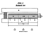
- FIG. 2 is a cross-sectional view of a bottom emission organic electroluminescent device according to the related art.
- FIG. 2 shows one pixel region including red, green, and blue sub-pixel regions.
- a first substrate 10 faces and is separated from a second substrate 30 .
- a peripheral portion of the first and second substrates 10 and 30 is sealed with a seal pattern 40 .
- a TFT T is formed at each sub-pixel region P sub on an inner surface of the first substrate 10 .
- a first electrode 12 is connected to the TFT T in each sub-pixel region.
- An organic electroluminescent layer 14 including luminescent materials that are red, green, or blue is formed on the TFT T and the first electrode 12 .
- a second electrode 16 is formed on the organic electroluminescent layer 14 .
- the first and second electrodes 12 and 16 apply an electric field to the organic electroluminescent layer 14 .
- An adhesive (not shown) and a moisture absorbent material (not shown) are formed on an inner surface of the second substrate 30 to shield the device from external moisture.
- a first electrode 12 functioning as an anode is made of a transparent conductive material
- a second electrode 16 functioning as a cathode includes a metallic material with a low work function.
- the organic electroluminescent layer 14 is composed of a hole injection layer 14 a , a hole transporting layer 14 b , an emission layer 14 c , and a electron transporting layer 14 d which cover the first electrode 12 .
- red, green, and blue emissive materials are alternately disposed at adjacent sub-pixel regions.
- green emissive material is disposed at sub-pixel P sub
- the adjacent sub-pixels have red emissive material and blue emissive material, respectively.
- FIG. 3 is a cross-sectional view showing one sub-pixel region of a bottom emission organic electroluminescent device according to the related art.
- a TFT T having a semiconductor layer 62 , a gate electrode 68 , a source electrode 80 and a drain electrode 82 is formed on a substrate 10 .
- the source electrode 80 of TFT T is connected to a storage capacitor C ST .
- the drain electrode 82 of TFT T is connected to an organic electroluminescent (EL) diode D EL .
- the storage capacitor C ST includes a power electrode 72 facing a capacitor electrode 64 .
- An insulating layer is interposed between the power electrode 72 and the capacitor electrode 64 .
- the capacitor electrode 64 includes the same material as the semiconductor layer 62 .
- the TFT T and the storage capacitor C ST are referred to as an array element A.
- the organic EL diode D EL includes a first electrode 12 facing a second electrode 16 , and an organic EL layer 14 interposed between the first electrode 12 and the second electrode 16 .
- the source electrode 80 of the TFT T is connected to the power electrode 72 of the storage capacitor C ST
- the drain electrode 82 of the TFT T is connected to the first electrode 12 of the organic EL diode D EL .
- the array element A and the EL diode D EL are formed on the same substrate in the organic electroluminescent device according to the related art.
- FIG. 4 is a flow chart showing a fabricating process of an organic electroluminescent device according to the related art.
- array element is formed on a first substrate.
- the array element includes a scanning line, a signal line, a power line, a switching TFT, and a driving TFT.
- the signal line is spaced apart from the power line, and the signal line and the power line each cross the scanning line.
- the switching TFT is disposed at the crossing point of the scanning line and the signal line.
- the driving TFT is disposed at the crossing point of the scanning line and the power line.
- a first electrode of an organic EL diode is formed over the array element.
- the first electrode is connected to the driving TFT of its respective sub-pixel region.
- an emission layer of the organic EL diode is formed on the first electrode.
- the organic EL layer may be composed of a hole injection layer, a hole transporting layer, an emission layer, and an electron transporting layer.
- a second electrode of the EL diode is formed on the organic EL layer.
- the second electrode is formed over an entire surface of the first substrate to function as a common electrode.
- the first substrate is encapsulated with a second substrate.
- the second substrate protects the first substrate from external impacts and prevents damage of the organic EL layer caused by air.
- a moisture absorbent material may be included in an inner surface of the second substrate.
- the organic EL device according to the related art is fabricated by encapsulating the first substrate including the array element and the organic EL diode with the second substrate. Since the production yield of the organic EL device is equal to the production yield of the array element multiplied by the production yield of the organic EL diode, the production yield for an organic EL device is limited by the process for the organic EL diode. Even if the array element is satisfactorily fabricated, the organic EL device may be faulty because the organic EL layer is defective. Accordingly, the expense of fabricating an array element properly and the associated material cost are lost and the production yield is reduced when organic EL diodes are improperly fabricated in an organic EL device according to the related art.
- Bottom emission organic EL devices have the advantages of high encapsulation stability and high process flexibility. However, bottom emission organic EL devices are ineffective for high resolution devices because they have poor aperture ratios. In contrast, a top emission organic EL device has a higher expected life span since it is easy to fabricate and has a high aperture ratio. However, in a top emission organic EL device, the cathode is generally formed on the organic EL layer. As a result, the transmittance and optical efficiency of a top emission organic EL device are reduced because of a limited number of materials that may be selected. When a thin film protection layer is used to minimize the transmittance reduction, the top emission organic EL device is not sufficiently shielded from ambient air.
- the present invention is directed to an organic electroluminescent device and a fabricating method thereof that substantially obviate one or more of the problems due to limitations and disadvantages of the related art.
- An object of the present invention is to provide an organic electroluminescent device including a first substrate that array element is formed thereon, a second substrate that an organic electroluminescent diode is formed thereon and a connection pattern electrically connecting the first and second substrates.
- An object of the present invention is to provide a top emission organic electroluminescent device that has a stable structure, and a fabricating method thereof.
- an organic electroluminescent device includes: a first substrate; a second substrate facing and spaced apart from the first substrate, the first and second substrates each having a pixel region; an array element on an inner surface of the first substrate, the array element including a plurality of thin film transistors within each pixel region; an organic electroluminescent diode on an inner surface of the second substrate; and a connection pattern electrically interconnecting the first and second substrates.
- a method of fabricating an organic electroluminescent device includes: forming an array element on a first substrate having a pixel region, the array element including a plurality of thin film transistors within each pixel region; forming an organic electroluminescent diode on a second substrate; forming a connection pattern to electrically interconnect the first substrate and the second substrate; and connecting the first substrate and the second substrate electrically with the connection pattern.
- FIG. 1 is an equivalent circuit diagram showing a basic pixel structure of an active matrix organic electroluminescent device according to the related art
- FIG. 2 is a cross-sectional view of a bottom emission organic electroluminescent device according to the related art
- FIG. 3 is a cross-sectional view showing one sub-pixel region of a bottom emission organic electroluminescent device according to the related art
- FIG. 4 is a flow chart showing a fabricating process of an organic electroluminescent device according to the related art
- FIG. 5 is a cross-sectional view of one pixel of an exemplary organic electroluminescent device according to the present invention.
- FIG. 6 is a flow chart of an exemplary fabricating process of an organic electroluminescent device according to the present invention.
- FIG. 5 is a cross-sectional view of one pixel of an exemplary organic electroluminescent device according to the present invention.
- a first substrate 110 may face and may be separated from a second substrate 130 .
- a seal pattern 140 may be formed along a peripheral portion between the first substrate 110 and the second substrate 130 .
- Array element 120 may be formed on an inner surface of the first substrate 110 and an organic electroluminescent (EL) diode D EL may be formed on an inner surface of the second substrate 130 .
- the organic EL diode D EL may include a first electrode 132 , an organic EL layer 134 , and a second electrode 136 .
- the first electrode may be formed on an inner surface of the second substrate 130 and may function as a common electrode.
- the organic EL layer 134 may be formed on the first electrode 132 , and the second electrode 136 may be formed on the organic EL layer 134 at each sub-pixel region P sub .
- the organic EL layer 134 may include a first organic material layer 134 a , an emission layer 134 b , and a second organic material layer 134 c .
- the first organic material layer 134 a may be formed on the first electrode 132 and the emission layer 134 b may be formed on the first organic layer 134 a .
- red, green, and blue emissive materials may be alternately disposed at adjacent sub-pixel regions. For example, in FIG.
- green emissive material is disposed at sub-pixel region P sub , while the adjacent sub-pixels have red emissive material and blue emissive material.
- the second organic material layer 134 c may be formed on the emission layer 134 b .
- the type of electroluminescent material to be used for the first and second organic material layers 134 a and 134 c may be determined according to the disposition of an anode and a cathode.
- the first organic material layer 134 a may include an electron injection layer and an electron transporting layer
- the second organic material layer 134 c may include a hole injection layer and a hole transporting layer.
- the first organic material layer 134 a may include a hole injection layer and a hole transporting layer
- the second organic material layer 134 c may include an electron injection layer and a electron transporting layer.
- the array element 120 may include a thin film transistor (TFT) T and a contact pattern 112 connected to the TFT T.
- the contact pattern 112 may be formed by extending an electrode of the TFT T or by patterning an additional metal layer.
- the TFT T may be a driving TFT connected to the organic EL diode D EL .
- a connection pattern 114 may be formed between the second electrode 136 and the contact pattern 112 in each sub-pixel region P sub .
- the connection pattern 114 may electrically connect the second electrode 136 and the TFT T.
- the connection pattern 114 may have a sufficient thickness and a sufficient area to contact the second electrode 136 and the contact pattern 112 .
- the connection pattern 114 may have a columnar structure.
- the connection pattern 114 may include a conductive material, which is preferably a flexible metallic material of low resistivity.
- the connection pattern 114 may be formed in conjunction with the formation of the array element 120 on the first substrate 110 .
- the top emission organic EL device may emit light through the second substrate 130 .
- the first electrode 132 may include a transparent or semi-transparent conductive material.
- the first electrode 132 may include a metallic material with a lower work function than a material of the second electrode 136 .
- the metallic material included in the first electrode 132 may be thin enough to transmit light.
- the metallic material may include at least one of aluminum (Al), aluminum:magnesium (Al:Mg) alloy, aluminum:lithium (Al:Li) alloy, and aluminum:benzonate alloy.
- the second electrode 136 may include an opaque conductive material that prevents the reflection of light toward the first substrate 100 .
- the first electrode 132 may include one of indium-tin-oxide (ITO) and indium-zinc-oxide (IZO).
- ITO indium-tin-oxide
- IZO indium-zinc-oxide
- a space between the array element 120 and the second electrode 136 may be filled with nitrogen gas (N 2 ) for example.
- the array element 120 may include a scanning line, a signal line, a power line, a switching TFT, and a storage capacitor.
- the signal line may be spaced apart from the power line, and the signal line and the power line may cross the scanning line.
- the switching TFT may be disposed where the signal line and the power line cross.
- a first substrate having an array element and a second substrate having an organic EL diode are individually provided, and the first and second substrates are connected by a connection pattern. Accordingly, an organic electroluminescent device with high resolution, a high aperture ratio, and improved production yield has been described.
- FIG. 6 is a flow chart of an exemplary fabricating process of an organic electroluminescent device according to the present invention.
- array elements which may include a switching element in each sub-pixel region, may be formed on a first substrate.
- a buffer layer may be formed on the first substrate, and a semiconductor layer and a capacitor electrode may be formed on the buffer layer.
- a gate electrode, a source electrode, and a drain electrode may be formed on the semiconductor layer.
- a power electrode connected to the source electrode may be formed over the capacitor electrode.
- a contact pattern contacting a connection pattern may be formed by extending the drain electrode or patterning an additional metal layer. The connection pattern may electrically connect the array element and a second electrode of an organic EL diode.
- connection pattern were formed on the organic electroluminescent diode over a second substrate, a photolithographic process may damage an organic EL layer of the organic EL diode. Therefore, it may be preferable to form the connection pattern on the array element in each sub-pixel region after forming the array element on the first substrate.
- the connection pattern may have a columnar structure.
- a first electrode of an organic EL diode may be formed on a second substrate. Since the first electrode is formed directly on the second substrate, a wider range of materials may be selected for the first electrode, and a fabricating process of the first electrode may be more easily performed.
- the first electrode may be made of a transparent conductive material.
- the first electrode may function as an anode and may include one of indium-tin-oxide (ITO) and indium-zinc-oxide (IZO).
- an organic EL layer may be formed on the first electrode.
- the organic EL layer may include an emission layer, an injection layer, and a transporting layer.
- the emission layer may be made of red, green, and blue emissive materials where the red, green, and blue emission layers may be alternately disposed at adjacent sub-pixel regions.
- the injection layer may inject a hole or an electron, and the transporting layer may transport a hole or an electron.
- the injection layer and the transporting layer may include a polymer.
- a second electrode may be formed on the organic EL layer.
- the second electrode may function as a cathode and may include an opaque metallic material.
- the first substrate may be electrically connected to the second substrate via the contact pattern and the connection pattern.
- one end of the connection pattern may contact either the switching element of the array element or the contact pattern connected to the switching element, and the other end of the connection pattern may contact the second electrode.
- the connection pattern may connect the driving TFT of the first substrate and the organic EL diode of the second substrate.
- the first and second substrates may be attached using a seal pattern formed along a peripheral portion between the first and second substrates.
- the array elements of the first substrate may be spaced apart from the second electrode of the second substrate, and the space between the array elements and the second electrode may be filled with nitrogen gas (N 2 ) for example.
- a moisture absorbent material 150 (of FIG. 5 ) preventing moisture from contacting the organic EL layer may be formed on either the first substrate or the second substrate adjacent to the seal pattern.
- the moisture absorbent material 150 may have a columnar structure similar to the seal pattern for example.
- the first substrate and the second substrate may be individually inspected after forming the array element and the organic EL diode, respectively, and then only first substrates and second substrates that pass inspection may be attached. Therefore, the production yield for an organic EL device is improved resulting in increased production efficiency and longer expected life spans for organic EL devices. Moreover, a top emission organic EL device with high resolution and a high aperture ratio results from the improved process. In addition, a larger range of materials may be selected for the electrode of the organic EL diode since it directly contacts with a substrate. Furthermore, since the organic electroluminescent layer of the organic EL diode is protected by a substrate, the device is more adequately protected from ambient air and moisture.
Landscapes
- Engineering & Computer Science (AREA)
- Microelectronics & Electronic Packaging (AREA)
- Electroluminescent Light Sources (AREA)
- Devices For Indicating Variable Information By Combining Individual Elements (AREA)
Applications Claiming Priority (3)
| Application Number | Priority Date | Filing Date | Title |
|---|---|---|---|
| KR10-2002-0009646 | 2002-02-22 | ||
| KR1020020009646A KR20030069707A (ko) | 2002-02-22 | 2002-02-22 | 유기전계발광 소자 및 그의 제조방법 |
| KRP2002-9646 | 2002-02-22 |
Publications (2)
| Publication Number | Publication Date |
|---|---|
| US20030160564A1 US20030160564A1 (en) | 2003-08-28 |
| US7755279B2 true US7755279B2 (en) | 2010-07-13 |
Family
ID=19719418
Family Applications (1)
| Application Number | Title | Priority Date | Filing Date |
|---|---|---|---|
| US10/331,320 Expired - Lifetime US7755279B2 (en) | 2002-02-22 | 2002-12-31 | Organic electroluminescent device and fabricating method thereof |
Country Status (8)
| Country | Link |
|---|---|
| US (1) | US7755279B2 (ja) |
| JP (1) | JP2003257667A (ja) |
| KR (1) | KR20030069707A (ja) |
| CN (1) | CN100544063C (ja) |
| DE (1) | DE10307504B4 (ja) |
| FR (1) | FR2836599B1 (ja) |
| GB (1) | GB2387482B (ja) |
| TW (1) | TW582187B (ja) |
Cited By (1)
| Publication number | Priority date | Publication date | Assignee | Title |
|---|---|---|---|---|
| US20110193475A1 (en) * | 2010-02-08 | 2011-08-11 | Samsung Mobile Display Co. Ltd. | Organic light emitting display and manufacturing method thereof |
Families Citing this family (37)
| Publication number | Priority date | Publication date | Assignee | Title |
|---|---|---|---|---|
| KR100426964B1 (ko) * | 2002-03-20 | 2004-04-13 | 엘지.필립스 엘시디 주식회사 | 유기전계발광 소자 및 그의 제조방법 |
| US7164155B2 (en) | 2002-05-15 | 2007-01-16 | Semiconductor Energy Laboratory Co., Ltd. | Light emitting device |
| US7105999B2 (en) | 2002-07-05 | 2006-09-12 | Lg.Philips Lcd Co., Ltd. | Organic electroluminescent display device and method of fabricating the same |
| KR100478759B1 (ko) * | 2002-08-20 | 2005-03-24 | 엘지.필립스 엘시디 주식회사 | 유기전계 발광소자와 그 제조방법 |
| KR100482166B1 (ko) * | 2002-08-26 | 2005-04-14 | 엘지.필립스 엘시디 주식회사 | 듀얼패널타입 유기전계발광 소자 및 그의 제조방법 |
| DE10357472B4 (de) * | 2002-12-13 | 2010-05-12 | Lg Display Co., Ltd. | Organisches Doppeltafel-Elektrolumineszenzdisplay und Verfahren zu dessen Herstellung |
| JP4497881B2 (ja) * | 2003-09-30 | 2010-07-07 | 三洋電機株式会社 | 有機el素子および有機elパネル |
| NL1025135C2 (nl) * | 2003-12-24 | 2005-08-30 | Lg Philips Lcd Co | Organische elektroluminescerende beeldweergevende inrichting en werkwijze voor het vervaardigen daarvan. |
| KR100557730B1 (ko) * | 2003-12-26 | 2006-03-06 | 엘지.필립스 엘시디 주식회사 | 듀얼패널타입 유기전계발광 소자 및 그 제조방법 |
| KR100642491B1 (ko) | 2003-12-26 | 2006-11-02 | 엘지.필립스 엘시디 주식회사 | 유기전계발광 소자 |
| KR100529846B1 (ko) * | 2003-12-26 | 2005-11-22 | 엘지.필립스 엘시디 주식회사 | 듀얼패널타입 유기전계발광 소자 및 그 제조방법 |
| FR2864701B1 (fr) * | 2003-12-26 | 2006-09-08 | Lg Philips Co Ltd | Dispositif d'affichage electroluminescent organique et son procede de fabrication |
| KR100556525B1 (ko) * | 2003-12-29 | 2006-03-06 | 엘지.필립스 엘시디 주식회사 | 유기전계 발광소자와 그 제조방법 |
| KR100583252B1 (ko) * | 2003-12-29 | 2006-05-24 | 엘지.필립스 엘시디 주식회사 | 유기전계 발광소자와 그 제조방법 |
| DE102004031109B4 (de) * | 2003-12-30 | 2016-03-31 | Lg Display Co., Ltd. | Organisches Lumineszenzdisplay vom Doppeltafeltyp sowie Verfahren zum Herstellen desselben |
| CN100452420C (zh) * | 2003-12-30 | 2009-01-14 | 乐金显示有限公司 | 双板型有机电致发光器件及其制造方法 |
| US7453426B2 (en) * | 2004-01-14 | 2008-11-18 | Semiconductor Energy Laboratory Co., Ltd. | Display device and electronic apparatus |
| US7315047B2 (en) * | 2004-01-26 | 2008-01-01 | Semiconductor Energy Laboratory Co., Ltd. | Light-emitting device |
| KR100652352B1 (ko) * | 2004-05-10 | 2006-12-01 | 엘지.필립스 엘시디 주식회사 | 유기전계발광 소자 및 그 제조방법 |
| KR20060046476A (ko) * | 2004-06-18 | 2006-05-17 | 산요덴키가부시키가이샤 | 일렉트로루미네센스 패널 |
| KR100594865B1 (ko) | 2004-08-10 | 2006-06-30 | 엘지.필립스 엘시디 주식회사 | 유기전계 발광소자와 그 제조방법 |
| JP4573672B2 (ja) * | 2005-02-28 | 2010-11-04 | 三洋電機株式会社 | 有機elパネル |
| US8969126B2 (en) | 2006-03-15 | 2015-03-03 | Lg Chem, Ltd. | Fabrication method for organic light emitting device and organic light emitting device fabricated by the same method |
| KR100747429B1 (ko) * | 2006-08-28 | 2007-08-08 | 주식회사 대우일렉트로닉스 | 오엘이디 디스플레이 소자 |
| KR100922062B1 (ko) * | 2008-02-15 | 2009-10-16 | 삼성모바일디스플레이주식회사 | 유기전계발광 표시장치 |
| KR20100010215A (ko) * | 2008-07-22 | 2010-02-01 | 엘지디스플레이 주식회사 | 유기발광 표시장치 및 그 제조 방법 |
| KR101436994B1 (ko) * | 2009-01-23 | 2014-09-11 | 삼성전자주식회사 | 접이식 디스플레이 장치 |
| KR101107178B1 (ko) * | 2009-07-20 | 2012-01-25 | 삼성모바일디스플레이주식회사 | 유기 발광 표시 장치 |
| CN104240610B (zh) * | 2010-10-14 | 2017-02-15 | 深圳华视光电有限公司 | 一种场致发光点驱动系统及其应用 |
| EP2579313B1 (en) | 2011-09-22 | 2021-10-27 | LG Display Co., Ltd. | Organic light emitting diode display device and method of fabricating the same |
| DE102013106815A1 (de) * | 2013-06-28 | 2014-12-31 | Osram Oled Gmbh | Optoelektronisches Bauelement und Verfahren zum Herstellen eines optoelektronischen Bauelementes |
| KR102399570B1 (ko) | 2015-11-26 | 2022-05-19 | 삼성디스플레이 주식회사 | 유기 발광 소자 |
| KR20170068705A (ko) * | 2015-12-09 | 2017-06-20 | 삼성디스플레이 주식회사 | 유기 발광 소자 |
| US11910707B2 (en) | 2015-12-23 | 2024-02-20 | Samsung Display Co., Ltd. | Organic light-emitting device |
| KR20170127101A (ko) | 2016-05-10 | 2017-11-21 | 삼성디스플레이 주식회사 | 유기 발광 소자 |
| KR20190108222A (ko) * | 2018-03-13 | 2019-09-24 | 삼성디스플레이 주식회사 | 유기 발광 소자 |
| CN109713165B (zh) * | 2019-01-15 | 2021-04-27 | 合肥京东方光电科技有限公司 | 显示面板及其制备方法 |
Citations (36)
| Publication number | Priority date | Publication date | Assignee | Title |
|---|---|---|---|---|
| US5756147A (en) * | 1992-05-08 | 1998-05-26 | Westaim Technologies, Inc. | Method of forming a dielectric layer in an electroluminescent laminate |
| US5837391A (en) * | 1996-01-17 | 1998-11-17 | Nec Corporation | Organic electroluminescent element having electrode between two fluorescent media for injecting carrier thereinto |
| EP0883191A2 (en) | 1997-06-02 | 1998-12-09 | Canon Kabushiki Kaisha | Electroluminescence device, electroluminescence apparatus, and production methods thereof |
| JPH10333601A (ja) | 1997-06-02 | 1998-12-18 | Canon Inc | エレクトロ・ルミネセンス素子及びその製造法 |
| WO1999003087A2 (en) | 1997-07-11 | 1999-01-21 | Fed Corporation | Bonded active matrix organic light emitting device display and method of producing the same |
| JPH11329743A (ja) | 1998-05-19 | 1999-11-30 | Stanley Electric Co Ltd | 電界発光素子およびその製造方法 |
| US6046547A (en) * | 1996-12-19 | 2000-04-04 | Sanyo Electric Co., Ltd. | Self-emission type image display device |
| US6075316A (en) * | 1997-12-15 | 2000-06-13 | Motorola, Inc. | Full color organic electroluminescent display device and method of fabrication |
| US6081071A (en) * | 1998-05-18 | 2000-06-27 | Motorola, Inc. | Electroluminescent apparatus and methods of manufacturing and encapsulating |
| US6091194A (en) | 1995-11-22 | 2000-07-18 | Motorola, Inc. | Active matrix display |
| JP2000208252A (ja) | 1999-01-14 | 2000-07-28 | Tdk Corp | 有機el素子 |
| JP2000306664A (ja) | 1999-04-21 | 2000-11-02 | Stanley Electric Co Ltd | 有機el表示装置 |
| JP2001035663A (ja) | 1999-07-27 | 2001-02-09 | Pioneer Electronic Corp | 有機エレクトロルミネッセンス素子表示装置及びその製造方法 |
| EP1085576A2 (en) | 1999-09-17 | 2001-03-21 | Sel Semiconductor Energy Laboratory Co., Ltd. | El display device and method for manufacturing the same |
| JP2001117509A (ja) | 1999-10-14 | 2001-04-27 | Nippon Hoso Kyokai <Nhk> | 有機el表示装置 |
| JP2001177509A (ja) | 1999-12-16 | 2001-06-29 | Oki Electric Ind Co Ltd | クロック載せ換え方法及び装置 |
| JP2001282123A (ja) | 2000-03-30 | 2001-10-12 | Toshiba Corp | 表示装置およびその製造方法 |
| US20010046611A1 (en) * | 1998-03-02 | 2001-11-29 | Junji Kido | Organic electroluminescent devices |
| US20020011783A1 (en) * | 2000-02-16 | 2002-01-31 | Idemitsu Kosan Co., Ltd | Active-driving organic el light emission device and process for producing the same |
| KR20020047889A (ko) | 2000-12-14 | 2002-06-22 | 김순택 | 유기 전계발광 디바이스 및 이의 제조 방법 |
| US6424094B1 (en) * | 2001-05-15 | 2002-07-23 | Eastman Kodak Company | Organic electroluminescent display with integrated resistive touch screen |
| WO2002078101A1 (en) | 2001-03-22 | 2002-10-03 | Microemissive Displays Limited | Method of creating an electroluminescent device |
| US20020158577A1 (en) | 2000-07-07 | 2002-10-31 | Tatsuya Shimoda | Organic electroluminescent display and manufacturing method thereof, electro-optic device and manufacturing method thereof, and electronic device |
| JP2003066859A (ja) | 2001-08-28 | 2003-03-05 | Sharp Corp | 表示装置およびその製造方法 |
| US6538390B2 (en) * | 2000-09-06 | 2003-03-25 | Sharp Kabushiki Kaisha | Organic LED display device of active matrix drive type and fabrication method therefor |
| US6548961B2 (en) * | 2001-06-22 | 2003-04-15 | International Business Machines Corporation | Organic light emitting devices |
| US6605826B2 (en) * | 2000-08-18 | 2003-08-12 | Semiconductor Energy Laboratory Co., Ltd. | Light-emitting device and display device |
| US6608449B2 (en) * | 2000-05-08 | 2003-08-19 | Semiconductor Energy Laboratory Co., Ltd. | Luminescent apparatus and method of manufacturing the same |
| US20030201712A1 (en) * | 2002-04-25 | 2003-10-30 | Lg.Philips Lcd Co., Ltd. | Organic electroluminescent display device and method of fabricating the same |
| US6737176B1 (en) * | 1999-07-15 | 2004-05-18 | Nec Corporation | Organic electroluminescent device and method for fabricating same |
| US6768257B1 (en) * | 1999-10-28 | 2004-07-27 | Sony Corporation | Display apparatus with ribs having conductive material |
| US6781746B2 (en) * | 2000-03-27 | 2004-08-24 | Semiconductor Energy Laboratory Co., Ltd. | Self-light emitting device and method of manufacturing the same |
| KR20040079476A (ko) | 2003-03-07 | 2004-09-16 | 엘지.필립스 엘시디 주식회사 | 유기전계 발광소자와 그 제조방법 |
| US6844673B1 (en) * | 2001-12-06 | 2005-01-18 | Alien Technology Corporation | Split-fabrication for light emitting display structures |
| US6885156B2 (en) * | 2000-07-24 | 2005-04-26 | Canon Kabushiki Kaisha | Electron-emitting device and image forming apparatus |
| US7176620B2 (en) * | 2002-09-26 | 2007-02-13 | Chi Mei Optoelectronics Corp. | Organic light-emitting device, organic light-emitting display apparatus, and method of manufacturing organic light-emitting display apparatus |
Family Cites Families (1)
| Publication number | Priority date | Publication date | Assignee | Title |
|---|---|---|---|---|
| US6215244B1 (en) * | 1997-06-16 | 2001-04-10 | Canon Kabushiki Kaisha | Stacked organic light emitting device with specific electrode arrangement |
-
2002
- 2002-02-22 KR KR1020020009646A patent/KR20030069707A/ko active Search and Examination
- 2002-12-31 US US10/331,320 patent/US7755279B2/en not_active Expired - Lifetime
-
2003
- 2003-02-13 GB GB0303349A patent/GB2387482B/en not_active Expired - Lifetime
- 2003-02-17 TW TW092103203A patent/TW582187B/zh not_active IP Right Cessation
- 2003-02-18 FR FR0301938A patent/FR2836599B1/fr not_active Expired - Lifetime
- 2003-02-20 CN CNB031054021A patent/CN100544063C/zh not_active Expired - Lifetime
- 2003-02-21 DE DE10307504A patent/DE10307504B4/de not_active Expired - Lifetime
- 2003-02-21 JP JP2003044274A patent/JP2003257667A/ja active Pending
Patent Citations (39)
| Publication number | Priority date | Publication date | Assignee | Title |
|---|---|---|---|---|
| US5756147A (en) * | 1992-05-08 | 1998-05-26 | Westaim Technologies, Inc. | Method of forming a dielectric layer in an electroluminescent laminate |
| US6091194A (en) | 1995-11-22 | 2000-07-18 | Motorola, Inc. | Active matrix display |
| US5837391A (en) * | 1996-01-17 | 1998-11-17 | Nec Corporation | Organic electroluminescent element having electrode between two fluorescent media for injecting carrier thereinto |
| US6046547A (en) * | 1996-12-19 | 2000-04-04 | Sanyo Electric Co., Ltd. | Self-emission type image display device |
| EP0883191A2 (en) | 1997-06-02 | 1998-12-09 | Canon Kabushiki Kaisha | Electroluminescence device, electroluminescence apparatus, and production methods thereof |
| JPH10333601A (ja) | 1997-06-02 | 1998-12-18 | Canon Inc | エレクトロ・ルミネセンス素子及びその製造法 |
| US6175345B1 (en) | 1997-06-02 | 2001-01-16 | Canon Kabushiki Kaisha | Electroluminescence device, electroluminescence apparatus, and production methods thereof |
| WO1999003087A2 (en) | 1997-07-11 | 1999-01-21 | Fed Corporation | Bonded active matrix organic light emitting device display and method of producing the same |
| US6075316A (en) * | 1997-12-15 | 2000-06-13 | Motorola, Inc. | Full color organic electroluminescent display device and method of fabrication |
| US20010046611A1 (en) * | 1998-03-02 | 2001-11-29 | Junji Kido | Organic electroluminescent devices |
| US6081071A (en) * | 1998-05-18 | 2000-06-27 | Motorola, Inc. | Electroluminescent apparatus and methods of manufacturing and encapsulating |
| JPH11329743A (ja) | 1998-05-19 | 1999-11-30 | Stanley Electric Co Ltd | 電界発光素子およびその製造方法 |
| JP2000208252A (ja) | 1999-01-14 | 2000-07-28 | Tdk Corp | 有機el素子 |
| JP2000306664A (ja) | 1999-04-21 | 2000-11-02 | Stanley Electric Co Ltd | 有機el表示装置 |
| US6737176B1 (en) * | 1999-07-15 | 2004-05-18 | Nec Corporation | Organic electroluminescent device and method for fabricating same |
| JP2001035663A (ja) | 1999-07-27 | 2001-02-09 | Pioneer Electronic Corp | 有機エレクトロルミネッセンス素子表示装置及びその製造方法 |
| EP1085576A2 (en) | 1999-09-17 | 2001-03-21 | Sel Semiconductor Energy Laboratory Co., Ltd. | El display device and method for manufacturing the same |
| JP2001117509A (ja) | 1999-10-14 | 2001-04-27 | Nippon Hoso Kyokai <Nhk> | 有機el表示装置 |
| US6768257B1 (en) * | 1999-10-28 | 2004-07-27 | Sony Corporation | Display apparatus with ribs having conductive material |
| JP2001177509A (ja) | 1999-12-16 | 2001-06-29 | Oki Electric Ind Co Ltd | クロック載せ換え方法及び装置 |
| US20020011783A1 (en) * | 2000-02-16 | 2002-01-31 | Idemitsu Kosan Co., Ltd | Active-driving organic el light emission device and process for producing the same |
| US6781746B2 (en) * | 2000-03-27 | 2004-08-24 | Semiconductor Energy Laboratory Co., Ltd. | Self-light emitting device and method of manufacturing the same |
| JP2001282123A (ja) | 2000-03-30 | 2001-10-12 | Toshiba Corp | 表示装置およびその製造方法 |
| US6608449B2 (en) * | 2000-05-08 | 2003-08-19 | Semiconductor Energy Laboratory Co., Ltd. | Luminescent apparatus and method of manufacturing the same |
| US20020158577A1 (en) | 2000-07-07 | 2002-10-31 | Tatsuya Shimoda | Organic electroluminescent display and manufacturing method thereof, electro-optic device and manufacturing method thereof, and electronic device |
| US6885156B2 (en) * | 2000-07-24 | 2005-04-26 | Canon Kabushiki Kaisha | Electron-emitting device and image forming apparatus |
| US6605826B2 (en) * | 2000-08-18 | 2003-08-12 | Semiconductor Energy Laboratory Co., Ltd. | Light-emitting device and display device |
| US6538390B2 (en) * | 2000-09-06 | 2003-03-25 | Sharp Kabushiki Kaisha | Organic LED display device of active matrix drive type and fabrication method therefor |
| KR20020047889A (ko) | 2000-12-14 | 2002-06-22 | 김순택 | 유기 전계발광 디바이스 및 이의 제조 방법 |
| US20020079494A1 (en) | 2000-12-14 | 2002-06-27 | Kim Hye-Dong | Organic EL device and method for manufacturing the same |
| WO2002078101A1 (en) | 2001-03-22 | 2002-10-03 | Microemissive Displays Limited | Method of creating an electroluminescent device |
| EP1371101A1 (en) | 2001-03-22 | 2003-12-17 | Microemissive Displays Limited | Method of creating an electroluminescent device |
| US6424094B1 (en) * | 2001-05-15 | 2002-07-23 | Eastman Kodak Company | Organic electroluminescent display with integrated resistive touch screen |
| US6548961B2 (en) * | 2001-06-22 | 2003-04-15 | International Business Machines Corporation | Organic light emitting devices |
| JP2003066859A (ja) | 2001-08-28 | 2003-03-05 | Sharp Corp | 表示装置およびその製造方法 |
| US6844673B1 (en) * | 2001-12-06 | 2005-01-18 | Alien Technology Corporation | Split-fabrication for light emitting display structures |
| US20030201712A1 (en) * | 2002-04-25 | 2003-10-30 | Lg.Philips Lcd Co., Ltd. | Organic electroluminescent display device and method of fabricating the same |
| US7176620B2 (en) * | 2002-09-26 | 2007-02-13 | Chi Mei Optoelectronics Corp. | Organic light-emitting device, organic light-emitting display apparatus, and method of manufacturing organic light-emitting display apparatus |
| KR20040079476A (ko) | 2003-03-07 | 2004-09-16 | 엘지.필립스 엘시디 주식회사 | 유기전계 발광소자와 그 제조방법 |
Non-Patent Citations (1)
| Title |
|---|
| Machine English translation of JP 2001-282123 to Nakajima et al. * |
Cited By (3)
| Publication number | Priority date | Publication date | Assignee | Title |
|---|---|---|---|---|
| US20110193475A1 (en) * | 2010-02-08 | 2011-08-11 | Samsung Mobile Display Co. Ltd. | Organic light emitting display and manufacturing method thereof |
| US8441181B2 (en) | 2010-02-08 | 2013-05-14 | Samsung Display Co., Ltd. | Organic light emitting display and manufacturing method thereof |
| US9039477B2 (en) | 2010-02-08 | 2015-05-26 | Samsung Display Co., Ltd. | Method of manufacturing an organic light emitting display |
Also Published As
| Publication number | Publication date |
|---|---|
| TW582187B (en) | 2004-04-01 |
| DE10307504A8 (de) | 2005-04-07 |
| GB2387482A (en) | 2003-10-15 |
| TW200303698A (en) | 2003-09-01 |
| GB0303349D0 (en) | 2003-03-19 |
| FR2836599B1 (fr) | 2007-04-13 |
| GB2387482B (en) | 2005-02-02 |
| CN1440223A (zh) | 2003-09-03 |
| DE10307504A1 (de) | 2003-09-04 |
| JP2003257667A (ja) | 2003-09-12 |
| FR2836599A1 (fr) | 2003-08-29 |
| KR20030069707A (ko) | 2003-08-27 |
| US20030160564A1 (en) | 2003-08-28 |
| CN100544063C (zh) | 2009-09-23 |
| DE10307504B4 (de) | 2010-04-29 |
Similar Documents
| Publication | Publication Date | Title |
|---|---|---|
| US7755279B2 (en) | Organic electroluminescent device and fabricating method thereof | |
| US7187118B2 (en) | Dual panel type organic electro luminescent display device and manufacturing method for the same | |
| KR100642491B1 (ko) | 유기전계발광 소자 | |
| US7518147B2 (en) | Organic electro luminescence device and fabrication method thereof | |
| US7132308B2 (en) | Dual panel-type organic electroluminescent display device and method of fabricating the same | |
| US6831298B2 (en) | Dual panel-type organic electroluminescent display device | |
| JP3993129B2 (ja) | 有機電界発光素子 | |
| US6922015B2 (en) | Organic electroluminescent display device and method of fabricating the same | |
| US7649311B2 (en) | Organic electroluminescent display device and method of fabricating the same | |
| KR100608403B1 (ko) | 유기전계발광 소자 및 그 제조방법 | |
| US7683538B2 (en) | Dual panel-type organic electroluminescent display device | |
| US10872948B2 (en) | Electroluminescent display device | |
| US6870197B2 (en) | Dual panel type organic electroluminescent display device and method of fabricating the same | |
| CN109979968B (zh) | 电致发光显示设备及其制造方法 | |
| KR100474000B1 (ko) | 듀얼패널타입 유기전계발광 소자 및 그의 제조방법 | |
| KR100726954B1 (ko) | 유기전계발광표시장치 및 그 제조방법 | |
| KR20100070802A (ko) | 듀얼플레이트 방식의 유기전계 발광소자 및 그 제조방법 |
Legal Events
| Date | Code | Title | Description |
|---|---|---|---|
| AS | Assignment |
Owner name: LG.PHILIPS LCD CO., LTD., KOREA, REPUBLIC OF Free format text: ASSIGNMENT OF ASSIGNORS INTEREST;ASSIGNORS:PARK, JAE-YONG;LEE, NAM-YANG;REEL/FRAME:013641/0940 Effective date: 20021220 |
|
| AS | Assignment |
Owner name: LG DISPLAY CO., LTD., KOREA, REPUBLIC OF Free format text: CHANGE OF NAME;ASSIGNOR:LG.PHILIPS LCD CO., LTD.;REEL/FRAME:021147/0009 Effective date: 20080319 Owner name: LG DISPLAY CO., LTD.,KOREA, REPUBLIC OF Free format text: CHANGE OF NAME;ASSIGNOR:LG.PHILIPS LCD CO., LTD.;REEL/FRAME:021147/0009 Effective date: 20080319 |
|
| FEPP | Fee payment procedure |
Free format text: PAYOR NUMBER ASSIGNED (ORIGINAL EVENT CODE: ASPN); ENTITY STATUS OF PATENT OWNER: LARGE ENTITY |
|
| STCF | Information on status: patent grant |
Free format text: PATENTED CASE |
|
| FPAY | Fee payment |
Year of fee payment: 4 |
|
| MAFP | Maintenance fee payment |
Free format text: PAYMENT OF MAINTENANCE FEE, 8TH YEAR, LARGE ENTITY (ORIGINAL EVENT CODE: M1552) Year of fee payment: 8 |
|
| MAFP | Maintenance fee payment |
Free format text: PAYMENT OF MAINTENANCE FEE, 12TH YEAR, LARGE ENTITY (ORIGINAL EVENT CODE: M1553); ENTITY STATUS OF PATENT OWNER: LARGE ENTITY Year of fee payment: 12 |