US7723779B2 - Integrated semiconductor nonvolatile storage device - Google Patents
Integrated semiconductor nonvolatile storage device Download PDFInfo
- Publication number
- US7723779B2 US7723779B2 US11/437,610 US43761006A US7723779B2 US 7723779 B2 US7723779 B2 US 7723779B2 US 43761006 A US43761006 A US 43761006A US 7723779 B2 US7723779 B2 US 7723779B2
- Authority
- US
- United States
- Prior art keywords
- gate
- field effect
- effect transistor
- semiconductor nonvolatile
- insulating film
- Prior art date
- Legal status (The legal status is an assumption and is not a legal conclusion. Google has not performed a legal analysis and makes no representation as to the accuracy of the status listed.)
- Active, expires
Links
- 239000004065 semiconductor Substances 0.000 title claims abstract description 95
- 238000003860 storage Methods 0.000 title claims abstract description 58
- 230000008672 reprogramming Effects 0.000 claims abstract description 9
- 238000009792 diffusion process Methods 0.000 claims description 68
- 230000005669 field effect Effects 0.000 claims description 54
- 239000000758 substrate Substances 0.000 claims description 36
- VYPSYNLAJGMNEJ-UHFFFAOYSA-N Silicium dioxide Chemical compound O=[Si]=O VYPSYNLAJGMNEJ-UHFFFAOYSA-N 0.000 claims description 25
- 229910052814 silicon oxide Inorganic materials 0.000 claims description 25
- 229910052581 Si3N4 Inorganic materials 0.000 claims description 19
- HQVNEWCFYHHQES-UHFFFAOYSA-N silicon nitride Chemical compound N12[Si]34N5[Si]62N3[Si]51N64 HQVNEWCFYHHQES-UHFFFAOYSA-N 0.000 claims description 19
- 230000014759 maintenance of location Effects 0.000 claims description 16
- 230000008859 change Effects 0.000 claims description 15
- 230000000717 retained effect Effects 0.000 claims description 12
- 230000006870 function Effects 0.000 claims description 11
- 238000000034 method Methods 0.000 description 52
- 230000008569 process Effects 0.000 description 33
- 238000010586 diagram Methods 0.000 description 27
- 229910021420 polycrystalline silicon Inorganic materials 0.000 description 25
- 229920005591 polysilicon Polymers 0.000 description 25
- 125000006850 spacer group Chemical group 0.000 description 20
- 229920002120 photoresistant polymer Polymers 0.000 description 13
- 229910052785 arsenic Inorganic materials 0.000 description 12
- RQNWIZPPADIBDY-UHFFFAOYSA-N arsenic atom Chemical compound [As] RQNWIZPPADIBDY-UHFFFAOYSA-N 0.000 description 12
- 238000002955 isolation Methods 0.000 description 9
- 238000004519 manufacturing process Methods 0.000 description 9
- 238000005530 etching Methods 0.000 description 8
- 101001084254 Homo sapiens Peptidyl-tRNA hydrolase 2, mitochondrial Proteins 0.000 description 7
- 102100030867 Peptidyl-tRNA hydrolase 2, mitochondrial Human genes 0.000 description 7
- 101100272590 Saccharomyces cerevisiae (strain ATCC 204508 / S288c) BIT2 gene Proteins 0.000 description 7
- 238000002347 injection Methods 0.000 description 7
- 239000007924 injection Substances 0.000 description 7
- XUIMIQQOPSSXEZ-UHFFFAOYSA-N Silicon Chemical group [Si] XUIMIQQOPSSXEZ-UHFFFAOYSA-N 0.000 description 6
- LPQOADBMXVRBNX-UHFFFAOYSA-N ac1ldcw0 Chemical compound Cl.C1CN(C)CCN1C1=C(F)C=C2C(=O)C(C(O)=O)=CN3CCSC1=C32 LPQOADBMXVRBNX-UHFFFAOYSA-N 0.000 description 6
- 239000012535 impurity Substances 0.000 description 6
- 238000011065 in-situ storage Methods 0.000 description 6
- 239000000969 carrier Substances 0.000 description 5
- 239000012212 insulator Substances 0.000 description 5
- 229910052710 silicon Inorganic materials 0.000 description 5
- 239000010703 silicon Substances 0.000 description 5
- 230000000694 effects Effects 0.000 description 4
- 238000000059 patterning Methods 0.000 description 4
- 229910021332 silicide Inorganic materials 0.000 description 4
- 230000015572 biosynthetic process Effects 0.000 description 3
- 239000002784 hot electron Substances 0.000 description 3
- BHEPBYXIRTUNPN-UHFFFAOYSA-N hydridophosphorus(.) (triplet) Chemical compound [PH] BHEPBYXIRTUNPN-UHFFFAOYSA-N 0.000 description 3
- 229910052751 metal Inorganic materials 0.000 description 3
- 239000002184 metal Substances 0.000 description 3
- 230000003647 oxidation Effects 0.000 description 3
- 238000007254 oxidation reaction Methods 0.000 description 3
- 230000001681 protective effect Effects 0.000 description 3
- FVBUAEGBCNSCDD-UHFFFAOYSA-N silicide(4-) Chemical compound [Si-4] FVBUAEGBCNSCDD-UHFFFAOYSA-N 0.000 description 3
- 238000003491 array Methods 0.000 description 2
- 230000015556 catabolic process Effects 0.000 description 2
- 239000002800 charge carrier Substances 0.000 description 2
- 238000006731 degradation reaction Methods 0.000 description 2
- 238000000151 deposition Methods 0.000 description 2
- 238000003795 desorption Methods 0.000 description 2
- 230000005684 electric field Effects 0.000 description 2
- 238000005516 engineering process Methods 0.000 description 2
- 239000000463 material Substances 0.000 description 2
- 230000009467 reduction Effects 0.000 description 2
- 230000005641 tunneling Effects 0.000 description 2
- 101001047515 Homo sapiens Lethal(2) giant larvae protein homolog 1 Proteins 0.000 description 1
- 102100022956 Lethal(2) giant larvae protein homolog 1 Human genes 0.000 description 1
- 101100237460 Rattus norvegicus Mgll gene Proteins 0.000 description 1
- 101100401357 Saccharomyces cerevisiae (strain ATCC 204508 / S288c) MGL2 gene Proteins 0.000 description 1
- 238000004140 cleaning Methods 0.000 description 1
- 230000008021 deposition Effects 0.000 description 1
- 230000007246 mechanism Effects 0.000 description 1
- 230000002093 peripheral effect Effects 0.000 description 1
Images


Classifications
-
- H—ELECTRICITY
- H01—ELECTRIC ELEMENTS
- H01L—SEMICONDUCTOR DEVICES NOT COVERED BY CLASS H10
- H01L29/00—Semiconductor devices specially adapted for rectifying, amplifying, oscillating or switching and having potential barriers; Capacitors or resistors having potential barriers, e.g. a PN-junction depletion layer or carrier concentration layer; Details of semiconductor bodies or of electrodes thereof ; Multistep manufacturing processes therefor
- H01L29/40—Electrodes ; Multistep manufacturing processes therefor
- H01L29/401—Multistep manufacturing processes
- H01L29/4011—Multistep manufacturing processes for data storage electrodes
- H01L29/40117—Multistep manufacturing processes for data storage electrodes the electrodes comprising a charge-trapping insulator
-
- H—ELECTRICITY
- H01—ELECTRIC ELEMENTS
- H01L—SEMICONDUCTOR DEVICES NOT COVERED BY CLASS H10
- H01L29/00—Semiconductor devices specially adapted for rectifying, amplifying, oscillating or switching and having potential barriers; Capacitors or resistors having potential barriers, e.g. a PN-junction depletion layer or carrier concentration layer; Details of semiconductor bodies or of electrodes thereof ; Multistep manufacturing processes therefor
- H01L29/66—Types of semiconductor device ; Multistep manufacturing processes therefor
- H01L29/68—Types of semiconductor device ; Multistep manufacturing processes therefor controllable by only the electric current supplied, or only the electric potential applied, to an electrode which does not carry the current to be rectified, amplified or switched
- H01L29/76—Unipolar devices, e.g. field effect transistors
- H01L29/772—Field effect transistors
- H01L29/78—Field effect transistors with field effect produced by an insulated gate
- H01L29/792—Field effect transistors with field effect produced by an insulated gate with charge trapping gate insulator, e.g. MNOS-memory transistors
-
- H—ELECTRICITY
- H10—SEMICONDUCTOR DEVICES; ELECTRIC SOLID-STATE DEVICES NOT OTHERWISE PROVIDED FOR
- H10B—ELECTRONIC MEMORY DEVICES
- H10B43/00—EEPROM devices comprising charge-trapping gate insulators
- H10B43/30—EEPROM devices comprising charge-trapping gate insulators characterised by the memory core region
-
- H—ELECTRICITY
- H10—SEMICONDUCTOR DEVICES; ELECTRIC SOLID-STATE DEVICES NOT OTHERWISE PROVIDED FOR
- H10B—ELECTRONIC MEMORY DEVICES
- H10B69/00—Erasable-and-programmable ROM [EPROM] devices not provided for in groups H10B41/00 - H10B63/00, e.g. ultraviolet erasable-and-programmable ROM [UVEPROM] devices
-
- G—PHYSICS
- G11—INFORMATION STORAGE
- G11C—STATIC STORES
- G11C16/00—Erasable programmable read-only memories
- G11C16/02—Erasable programmable read-only memories electrically programmable
- G11C16/04—Erasable programmable read-only memories electrically programmable using variable threshold transistors, e.g. FAMOS
- G11C16/0408—Erasable programmable read-only memories electrically programmable using variable threshold transistors, e.g. FAMOS comprising cells containing floating gate transistors
- G11C16/0425—Erasable programmable read-only memories electrically programmable using variable threshold transistors, e.g. FAMOS comprising cells containing floating gate transistors comprising cells containing a merged floating gate and select transistor
Definitions
- the present invention relates to a semiconductor storage device with a nonvolatile memory structure that is stable in operation.
- One of the built-in integrated semiconductor storage devices of an LSI is nonvolatile memory. This memory is very important in order to use the LSI in various applications, since it can retain stored data even after power to the LSI is removed.
- Nonvolatile semiconductor memory devices employing a floating gate or an insulating film are described in, for example, S. Sze, “Physics of Semiconductor Devices”, 2nd edition, Wiley-Interscience pub., p. 496-506 (Nonpatent Document 1).
- the type of nonvolatile memory in which an insulating film is laminated to store charges in the traps at the interface and in the insulating film does not require an additional conductive layer and hence can be formed in a manner matching the CMOS LSI process.
- this type of nonvolatile memory in which charges are retained within the insulating film must maintain sufficient charge retention characteristics while injecting or releasing charge, which is difficult to practically achieve.
- Nonpatent Document 3 1997 Symposium on VLSI Technology, 1997, p. 63-64.
- each cell includes two separate gates: a polysilicon gate for memory operation and a gate for memory cell selection.
- Similar memory devices are disclosed in U.S. Pat. No. 5,969,383 (Patent Document 1) and U.S. Pat. No. 6,477,084 (Patent Document 2).
- FIG. 1C An equivalent circuit is shown in FIG. 1C .
- a select transistor 1 and a memory transistor 2 are connected in series.
- FIGS. 1A and 1B show a plan view and a cross-sectional view, respectively, of the memory device or cell shown in FIG. 1C .
- FIG. 1A shows the arrangement of a select gate pattern 1500 , a memory gate pattern 1550 , and an active region pattern 1150 on the substrate of the memory device.
- FIG. 1B shows a cross-sectional view of the memory device, as described above. Referring to FIG.
- a gate 500 of the select transistor (hereinafter referred to as a select gate 500 ) and a gate 550 of the memory transistor (hereinafter referred to as a memory gate 550 ) are formed on a semiconductor substrate 100 .
- Diffusion layer electrodes 200 and 300 constituting the electrode portions of the memory device are formed in the semiconductor substrate 100 .
- a spacer insulator 940 is formed on a sidewall of each gate 500 , 550 , and diffusion layers 310 and 210 are formed in the semiconductor substrate 100 .
- reference numeral 900 denotes the gate insulating film of the select transistor and 950 denotes the gate insulating film of the memory transistor.
- a gate namely, the memory gate may be formed in a process called a spacer process, as shown in FIG. 1B .
- the gate insulating film 950 of the memory gate 550 is formed.
- the wafer is anisotropically etched in a direction perpendicular to its surface to form the memory gate 550 on a side of the select gate 500 .
- This process is hereinafter referred to as a spacer process.
- FIG. 2 shows an array arrangement of memory cells (BIT 1 , BIT 2 ) each represented by the equivalent circuit shown in FIG. 1C .
- FIG. 2 shows an array arrangement of memory cells (BIT 1 , BIT 2 ) each represented by the equivalent circuit shown in FIG. 1C .
- the gates of the select transistors 1 of the first-row memory cells constitute a word line SGL 0
- the gates of the memory transistors 2 of the first-row memory cells constitute a word line MGL 0
- the gates of the select transistors 1 of the second-row memory cells constitute a word line SGL 1
- the gates of the memory transistors 2 of the second-row memory cells constitute a word line MGL 1
- the gates of the select transistors 1 of the third-row memory cells (BIT 1 , BIT 2 , and so on) constitute a word line SGL 2
- the gates of the memory transistors 2 of the third-row memory cells constitute a word line MGL 2 ; and so on.
- the diffusion layers of the select transistors 1 of the first-column memory cells constitute a bit line BL 0
- the diffusion layers of the memory transistors 2 of the first-column memory cells constitute a source line SL 0
- the diffusion layers of the select transistors 1 of the second-column memory cells constitute a bit line BL 1
- the diffusion layers of the memory transistors 2 of the second-column memory cells constitute a source line SL 1 ; and so on.
- the first-row memory cells (BIT 1 , BIT 2 , and so on) may be denoted collectively by reference numeral WORD 1
- the second-row memory cells (BIT 1 , BIT 2 , and so on) may be denoted collectively by reference numeral WORD 2 , as shown in FIG. 2 .
- FIGS. 3 and 4 are schematic cross-sectional views of a memory cell portion, illustrating exemplary program or write and erase operations on the memory cell. These figures schematically show the memory cell structure and the program and erase operations and do not show the detailed structure. It should be noted that in FIGS. 3 and 4 , components common to FIG. 1B are designated by the same reference numerals.
- the gate insulating film 950 of the memory gate has a structure in which a silicon nitride film is sandwiched between silicon oxide films; that is, it has the so-called MONOS (Metal-Oxide-Nitride-Oxide Semiconductor (silicon)) structure.
- the gate insulating film 900 of the select gate is a silicon oxide film.
- the diffusion layer electrodes 200 and 300 are formed using the select gate 500 and the memory gate 550 as masks.
- FIG. 3 schematically shows a program or write operation.
- a positive potential is applied to the diffusion layer electrode 200 on the memory gate side, and ground potential is applied to the substrate 100 and the diffusion layer electrode 300 on the select gate side.
- a gate overdrive voltage higher than the voltage of the substrate 100 is applied to the memory gate 550 to set the channel under the memory gate 550 to an “on” state.
- the potential of the select gate 500 is set 0.1-0.2 V higher than the threshold voltage to cause the channel to assume the “on” state.
- a conductive state is established to allow electrons to move, as shown in FIG. 3 . Since in this state the highest electric field is produced around the boundary between the two gates, a number of hot electrons are generated and injected into the memory gate side.
- the white circle under the select gate 500 indicates an electron, a channel electron. This electron is accelerated to become a hot electron which is then injected into the MONOS film, as indicated by the arrow in the figure.
- Reference numeral 800 indicates generation of carriers due to impact ionization. The generated electron and hole, carriers, are indicated by a white circle and a shaded circle, respectively.
- This phenomenon is known as source side injection (SSI) and has been reported by, for example, A. T. Wu et al. (1986 IEEE International Electron Device Meeting, Technical Digest, 1986, p. 584-587 (Nonpatent Document 4)).
- SSI source side injection
- the injection mechanism also applies to “insulator film type” memory cells.
- This type of hot electron injection is characterized in that since the electric field is concentrated around the boundary between the select gate and the memory gate, the injection occurs predominantly at the select gate side portion of the memory gate.
- “insulator film type” memory retains charge within an insulating film. This means that in the case of “insulator film type” memory, electrons are retained within a very narrow region.
- FIG. 4 schematically shows an erase operation.
- a negative potential is applied to the memory gate 550 and a positive potential is applied to the diffusion layer electrode 200 on the memory gate side to cause strong inversion at the overlap between the memory gate and the diffusion layer.
- Band-to-band tunneling is described by, for example, T. Y. Chan et al. (1987 IEEE International Electron Device Meeting, Technical Digest, p. 718-721 (Nonpatent Document 5)).
- the generated holes are accelerated in the channel direction, attracted toward the memory gate by its bias, and thereby injected into the MONOS film, resulting in an erase operation.
- Reference numeral 820 indicates an electron-hole pair generated by a generated hole. These carriers are also injected into the MONOS film. That is, the threshold voltage of the memory gate that has been increased due to the negative charge of the injected electrons can be lowered by the positive charge of injected holes.
- a positive potential is applied to the diffusion layer electrode 300 on the select gate side and a positive potential is applied to the select gate 500 to set the channel under the select gate to an “on” state.
- the data retained in the form of charge can be read as a current by applying a memory gate potential intermediate between the threshold voltages in the program or write and erase states.
- this memory cell is made up of two transistors: the select transistor 1 and the memory transistor 2 .
- a common MOS transistor can be used as the select transistor 1 .
- the select transistor 1 may have a high performance device structure highly optimized for the manufacturing process. Therefore, to increase the cell current, it is important to enhance the performance of the memory transistor 2 .
- Increasing the current drive in a MOS transistor requires a reduction in the thickness of the gate insulating film or in the channel length if the same voltage conditions are applied to the transistor.
- the channel length is the gate length minus the overlap length between the gate and the diffusion layer, as described later (see FIG. 21A ).
- the memory gate structure shown in FIG. 1B formed by the so-called spacer process may be effective in reducing the channel length of a memory gate.
- the gate length of a memory gate formed by this process depends on the deposition thickness of the memory gate material. Therefore, this process allows formation of a gate having a gate length smaller than the minimum lithographic dimension of general lithographic technology, resulting in reduced channel length and hence increased current drive, as shown in FIG. 5 .
- FIG. 5 shows the relationship between the memory gate bias and the read current for several memory gate lengths (Lmg). Specifically, FIG. 5 compares the current drive levels obtained when the gate length is set to 50 nm, 60 nm, and 70 nm with a minimum lithographic dimension of 130 nm. The figure indicates that the current drive can be increased by reducing the gate length.
- FIG. 6 shows the relationship between the interface state intensity and the shift in the threshold voltage for two channel lengths (20 nm, 40 nm) with the same damaged layer width.
- the horizontal axis represents the interface state intensity
- the vertical axis represents the shift in the threshold voltage.
- the memory cell having the shorter channel length exhibits a larger threshold voltage shift. That is, the shorter the channel length, the larger the shift in the threshold voltage due to damage to the insulating film and its interface.
- the present invention has been devised to solve the above problems. It is, therefore, an object of the present invention to provide an integrated semiconductor nonvolatile storage device employing nonvolatile memory devices that allow for high performance and stable operation.
- Nonvolatile memory devices used in integrated semiconductor devices are broadly divided into two types depending on the requirements of the system: those adapted to be read at high speed and those adapted to be reprogrammed repeatedly.
- a typical example of the former is a memory device called a code file, which is used to store processing programs.
- a typical example of the latter is a memory device called a data file, which is used to store data.
- the code file is required to perform a read operation at high speed, while the data file is required to allow a number of reprogramming operations.
- a memory cell portion that must operate at high speed is also referred to as a code file
- a memory cell portion that must allow for a number of reprogramming operations is also referred to as a data file.
- a nonvolatile memory device may have one of the following chip configurations depending on the application.
- a code file nonvolatile memory chip and a data file nonvolatile memory chip are provided separately from the processing chip, as shown in FIG. 7 .
- the chip having a processing function includes code file nonvolatile memory, and a data file nonvolatile memory chip is separately provided, as shown in FIG. 8 .
- Some control systems require a data file memory space which is small but subjected to a number of reprogramming operations.
- they may employ a chip configuration in which the chip having a processing function includes data file memory, and a code file nonvolatile memory chip is separately provided, as shown in FIG. 9 .
- a split-gate memory cell of the present invention can be changed by changing the gate length of its memory gate, as described above. Therefore, according to the present invention, memory cells having different memory gate channel lengths are formed on the same chip to produce a single integrated semiconductor device by using various manufacturing processes described later in connection with preferred embodiments of the present invention. More specifically, memory cells that must be read at high speed have a shorter memory gate channel length, while those that must be reprogrammed many times have a longer memory gate channel length. These two types of memory cells are integrated on the same chip.
- the prevent invention can provide an integrated semiconductor nonvolatile storage device adapted for both high-speed read operation and repeated reprogramming.
- FIG. 1A is a plan view illustrating an exemplary layout of a split memory cell.
- FIG. 1B is a cross-sectional view illustrating an exemplary structure of the split memory cell.
- FIG. 1C is an equivalent circuit diagram of the split memory cell.
- FIG. 2 is an equivalent circuit diagram of a memory array of split memory cells.
- FIG. 3 is a schematic cross-sectional view illustrating a memory cell structure and a program operation.
- FIG. 4 is a schematic cross-sectional view illustrating a memory cell structure and an erase operation.
- FIG. 5 is a current-voltage characteristic graph illustrating the dependence of a read current on the memory gate length.
- FIG. 6 is a graph illustrating the dependence of the change in threshold voltage on the memory gate length.
- FIG. 7 is a diagram showing a chip configuration.
- FIG. 8 is a diagram showing another chip configuration.
- FIG. 9 is a diagram showing still another chip configuration.
- FIG. 10 is a diagram showing the configuration of a chip including a plurality of memory files.
- FIG. 11 is an equivalent circuit diagram of a memory array.
- FIG. 12 is a plan view showing the layout of the memory array.
- FIGS. 13 to 20 are cross-sectional structural views illustrating sequential process steps for forming a device according to a first embodiment of the present invention.
- FIG. 21A is a cross-sectional structural view illustrating the effect of the first embodiment.
- FIG. 21B is another cross-sectional structural view illustrating the effect of the first embodiment.
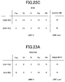
- FIG. 22A is a diagram showing programming conditions.
- FIG. 22B is a diagram showing erase conditions.
- FIG. 22C is a diagram showing read conditions.
- FIG. 23A is a diagram showing programming conditions.
- FIG. 23B is a diagram showing erase conditions.
- FIG. 23C is a diagram showing read conditions.
- FIG. 24A is a diagram showing programming conditions.
- FIG. 24B is a diagram showing erase conditions.
- FIG. 24C is a diagram showing read conditions.
- FIG. 25A is a diagram showing programming conditions.
- FIG. 25B is a diagram showing erase conditions.
- FIG. 25C is a diagram showing read conditions.
- FIGS. 26 to 33 are cross-sectional structural views illustrating sequential process steps for forming a device according to a second embodiment of the present invention.
- FIGS. 34 to 41 are cross-sectional structural views illustrating sequential process steps for forming a device according to a third embodiment of the present invention.
- FIG. 42 is a cross-sectional structural view illustrating the effect of the third embodiment.
- FIG. 43 is a diagram showing a memory file configuration.
- FIG. 44 is a diagram showing another memory file configuration.
- FIG. 45 is a diagram showing still another memory file configuration.
- FIG. 46 is a cross-sectional view showing memory cells according to a fifth embodiment of the present invention.
- FIG. 10 is a diagram showing the overall configuration of an integrated semiconductor device according to a first embodiment of the present invention.
- a code file portion 13 that must be read at high speed and a data file portion 14 that must be reprogrammed repeatedly are connected to a processing circuit portion or CPU 15 .
- CPU 15 a processing circuit portion or CPU 15 .
- FIG. 10 only shows the CPU 15 and the nonvolatile memory portions 13 and 14 to which the present invention is directed.
- the integrated semiconductor device also includes cache memory, general memory, I/O portions, and other necessary regions. These components have been omitted from the figure for clarity of explanation.
- FIGS. 11 to 20 are various schematic diagrams illustrating a memory cell array of the semiconductor device according to the first embodiment of the present invention.
- FIG. 11 is an equivalent circuit diagram of the memory cell array
- FIG. 12 is a plan view showing the layout of the memory cell array
- FIGS. 13 to 20 are cross-sectional views showing sequential process steps for forming the memory cell array.
- the illustration (a) on the left-hand side is a cross-sectional view of data file cells
- the illustration (b) on the right-hand side is a cross-sectional view of code file cells.
- an active region and device isolation regions are formed in the surface of a semiconductor substrate by a common shallow trench isolation (STI) process. It should be noted that these device isolation regions are not shown in the figures.
- the substrate surface 100 is thermally oxidized to form a gate insulating film 900 having a thickness of 2.5 nm, and a polysilicon layer is deposited to a thickness of 200 nm by a CVD technique.
- the polysilicon layer is etched to form select gate electrodes 500 , as shown in illustrations (a) and (b) of FIG. 13 .
- the gate electrodes in the processing circuit portion (CPU) may be formed at the same time as the above select gate electrodes.
- the exposed substrate surfaces are oxidized to a depth of 4 nm to form an oxide film 951 .
- a silicon nitride film 952 is deposited to a thickness of 8 nm, and a silicon oxide film 953 is deposited on the silicon nitride film 953 to a thickness of 7 nm, forming an ONO film 950 , as shown in illustrations (a) and (b) of FIG. 14 . That is, the ONO film 950 is a film stack made up of the oxide film 951 , the silicon nitride film 952 , and the silicon oxide film 953 .
- the ONO film can also be formed by an in-situ steam generation (ISSG) oxidation technique. That is, the substrate surface is ISSG-oxidized to a depth of 5 nm. Then, a silicon nitride film is deposited to a thickness of 14 nm and ISSG-oxidized to form an upper oxide film having a thickness of 6 nm.
- ISSG in-situ steam generation
- a polysilicon layer is deposited to a thickness of 70 nm.
- This polysilicon layer is doped with phosphorous to a high concentration in situ.
- This polysilicon layer is anisotropically etched to form a spacer-shaped memory gate 550 on a side of each select gate 500 .
- the contact forming portions may be masked with a photoresist pattern. Though not shown, additional etching may be performed to remove unwanted portions of the polysilicon 550 from the sides of the select gates.
- the ONO film 950 can be used as a protective film for protecting the underlayer. After etching off the exposed portions of the ONO film, the substrate surface is cleaned and then thermally oxidized to form an oxide film having a thickness of 2 nm. This oxide film is not shown in the figure, since it is substantially removed in subsequent steps. For example, in the step shown in FIG. 18 , the oxide film is substantially removed by surface cleaning.
- each mask layer formed of a photoresist is hereinafter denoted by symbol PR.
- a new mask layer PR or a photoresist layer is formed, and arsenic is ion-implanted in the diffusion layer region on the memory gate 550 side of each memory cell in the data file portion at 3 KeV to a dose amount of 10 15 cm ⁇ 2 to form sources (diffusion layer electrodes) 202 , as shown in FIG. 16 .
- drains diffusion layer electrodes 300 , as shown in FIG. 17 .
- each two memory cell portions in a side-by-side arrangement use the same drain region 300 as their drains.
- the formation of these drains may be combined with the above two source diffusion layer forming processes, as necessary.
- the diffusion layers in the processing circuit portion (CPU) may be formed at the same time as the above drains.
- the semiconductor substrate 100 thus processed is cleaned. In this step, most of the oxide film formed on the surface is removed, as described above. Then, a silicon oxide film is newly deposited to a thickness of 100 nm. This silicon oxide film is anisotropically etched to form a spacer 940 on a side of each select gate 500 and a side of each memory gate 550 . Then, arsenic is ion-implanted using these spacers 940 as masks to form diffusion layers 210 and 310 , as shown in FIG. 18 . It should be noted that the select gates 500 may be doped with an impurity at the same time with the above impurity doping. These processes are common lightly-doped drain (LDD) processes.
- LDD lightly-doped drain
- silicide layers 650 , 655 , 620 , and 630 are formed on the select gates, the memory gates, the source diffusion layers and the drain diffusion layers, respectively, by a common salicide process, as shown in FIG. 19 .
- this salicide process covers the sides of the polysilicon gates with spacer insulators, and selectively silicides the exposed top surfaces of the gates and the source and drain diffusion layer regions formed in the silicon substrate.
- the top surfaces of the select gates and the memory gates are silicided at once.
- reference numeral 700 denotes a contact plug and 750 denotes a first metal wiring layer.
- FIG. 21A is a cross-sectional view of a major portion of a memory cell in the data file portion
- FIG. 21B is a cross-sectional view of a major portion of a memory cell in the code file portion.
- FIGS. 21A and 21B components common to the above figures are designated by the same reference numerals. As can be seen by comparison between FIGS. 21A and 21B , these memory cells have the same memory gate length (Lmg) but different memory gate channel lengths (Leff). It should be noted that reference numeral Lcg denotes a select gate channel length.
- FIGS. 22A , 22 B, and 22 C show typical programming, erase, and read conditions.
- Vmg is memory gate voltage
- Vd bit line voltage
- Vs source line voltage
- Vcg select gate voltage
- Vbb substrate potential
- an erase operation is performed so as to produce a lower threshold voltage, as compared to an erase operation in the data file portion.
- this is achieved by increasing the width of the erase pulse.
- the memory gate voltage (Vmg) in the code file portion may be reduced as shown in FIGS. 23A , 23 B, and 23 C, or the diffusion layer voltage (Vs) in the code file portion may be increased as shown in FIGS. 24A , 24 B, and 24 C to achieve the same effect.
- Vmg memory gate voltage
- Vs diffusion layer voltage
- FIGS. 26 to 33 are cross-sectional views showing sequential process steps for forming a memory cell array.
- the illustration (a) on the left-hand side is a cross-sectional view of data file cells
- the illustration (b) on the right-hand side is a cross-sectional view of code file cells.
- These cross-sectional views are taken along line A-A of FIG. 12 in the channel direction.
- the code file portion and the data file portion can be designed to have the same array layout viewed in plan. Therefore, the present embodiment will be described with reference to the layout shown in FIG. 12 .
- an active region and device isolation regions are formed in the surface of a semiconductor substrate by a common shallow trench isolation (STI) process. It should be noted that these device isolation regions are not shown in the figures.
- the substrate surface is thermally oxidized to form a gate insulating film 900 having a thickness of 2.5 nm.
- a polysilicon layer 500 is deposited to a thickness of 200 nm by a CVD technique.
- the polysilicon layer is etched to form select gate electrodes 500 , as shown in FIG. 26 .
- the gate electrodes in the processing circuit portion (CPU) may be formed at the same time as the above select gate electrodes 500 .
- the exposed substrate surfaces are oxidized to a depth of 4 nm.
- a silicon nitride film is deposited on the top surface to a thickness of 8 nm, and a silicon oxide film is deposited on the silicon nitride film to a thickness of 7 nm, forming an ONO film, as shown in FIG. 27 .
- the ONO film can also be formed by an in-situ steam generation (ISSG) oxidation technique. That is, the substrate surface is ISSG-oxidized to form a silicon oxide film having a thickness of 5 nm. Then, a silicon nitride film is deposited to a thickness of 14 nm and ISSG-oxidized to form an upper oxide film having a thickness of 6 nm.
- ISSG in-situ steam generation
- a polysilicon layer is deposited to a thickness of 70 nm.
- This polysilicon layer is doped with phosphorous to a high concentration in situ.
- This polysilicon layer is anisotropically etched to form a spacer-shaped memory gate 550 on a side of each select gate 500 .
- the contact forming portions may be masked with a photoresist pattern. Though not shown, additional etching may be performed to remove unwanted portions of the polysilicon 550 from the sides of the select gates.
- the memory gates 550 are formed on only one side of each select gate 500 , the unwanted portions of the polysilicon 550 are removed by etching.
- the ONO film 950 can be used as a protective film for protecting the underlayer. After etching off the exposed portions of the ONO film, the substrate surface is cleaned and then thermally oxidized to form an oxide film having a thickness of 2 nm. This oxide is not shown in the figure, since it is substantially removed in subsequent steps.
- drains 300 a mask layer PR or a photoresist layer is formed, and arsenic is ion-implanted in the diffusion layer region on the select gate side of each memory cell in the code file portion and the data file portion at 5 KeV to a dose amount of 8 ⁇ 10 14 cm ⁇ 2 to form drains 300 .
- the formation of these drains may be combined with two source diffusion layer forming processes, as necessary. Further, the diffusion layers in the processing circuit portion (CPU) may be formed at the same time as the above drains.
- a new mask layer PR or a photoresist layer is formed, and arsenic is ion-implanted in the diffusion layer region on the memory gate side of each memory cell in the code file portion at 5 KeV to a dose amount of 8 ⁇ 10 15 cm ⁇ 2 to form sources 201 , as shown in FIG. 28 .
- a silicon oxide film is deposited to a thickness of 20 nm and anisotropically etched to form a spacer 941 on a side of each select gate 500 and a side of each memory gate 550 , as shown in FIG. 29 .
- a silicon oxide film is deposited to a thickness of 100 nm. This silicon oxide film is anisotropically etched to form a spacer 942 on a side of each select gate 500 and a side of each memory gate 550 . Then, arsenic is ion-implanted using these spacers 942 as masks to form diffusion layers 210 and 310 , as shown in FIG. 31 . It should be noted that the select gates 500 may be doped with an impurity at the same time with the above impurity doping. These processes are common lightly-doped drain (LDD) processes.
- LDD lightly-doped drain
- silicide layers 650 , 655 , 620 , and 630 are formed on the select gates, the memory gates, the source diffusion layers, and the drain diffusion layers, respectively, by a common salicide process, as shown in FIG. 32 .
- reference numeral 700 denotes a contact plug and 750 denotes a first metal wiring layer.
- the above manufacturing process allows the memory-gate-side diffusion layer regions in the data file portion having a double spacer arrangement to extend under their respective gates a smaller distance than the memory-gate-side diffusion layer regions in the code file portion. As a result, the memory gate of each memory cell in the data file portion has a longer effective channel length.
- FIGS. 34 to 42 are cross-sectional views showing sequential process steps for manufacturing a memory cell array.
- the illustration (a) on the left-hand side is a cross-sectional view of data file cells
- the illustration (b) on the right-hand side is a cross-sectional view of code file cells.
- These cross-sectional views are taken along line A-A of FIG. 12 in the channel direction.
- the code file portion and the data file portion can be designed to have the same array layout viewed in plan. Therefore, the present embodiment will be described with reference to the layout shown in FIG. 12 .
- an active region and device isolation regions are formed in the surface of a semiconductor substrate by a common shallow trench isolation (STI) process. It should be noted that these device isolation regions are not shown in the figures.
- the substrate surface is thermally oxidized to form a gate insulating film 900 having a thickness of 2.5 nm.
- a polysilicon layer 500 is deposited to a thickness of 200 nm by a CVD technique.
- the polysilicon layer is etched to form select gate electrodes 500 , as shown in FIG. 34 .
- the gate electrodes in the processing circuit portion (CPU) may be formed at the same time as the above select gate electrodes 500 .
- the exposed substrate surfaces are oxidized to a depth of 4 nm.
- a silicon nitride film is deposited on this oxide film to a thickness of 8 nm, and a silicon oxide film is deposited on the silicon nitride film to a thickness of 7 nm, forming an ONO film 950 .
- the ONO film can also be formed by an in-situ steam generation (ISSG) oxidation technique. That is, the substrate surface is ISSG-oxidized to form an oxide film having a thickness of 5 nm. Then, a silicon nitride film is deposited on the top surface to a thickness of 14 nm and ISSG-oxidized to form an upper oxide film having a thickness of 6 nm.
- ISSG in-situ steam generation
- a polysilicon layer is deposited to a thickness of 70 nm.
- This polysilicon layer is doped with phosphorous to a high concentration in situ.
- This polysilicon layer is anisotropically etched to form a spacer-shaped memory gate 550 on a side of each select gate 500 .
- the contact forming portions may be masked with a photoresist pattern.
- additional etching may be performed to remove unwanted portions of the polysilicon layer 550 from the sides of the select gates.
- the ONO film 950 can be used as a protective film for protecting the underlayer.
- a mask layer PR or a photoresist layer is formed, and arsenic is ion-implanted in the diffusion layer region on the memory gate side of each memory cell in the code file portion at 5 KeV to a dose amount of 10 15 cm ⁇ 2 to form sources 201 , as shown in FIG. 36 .
- a polysilicon layer is deposited to a thickness of 20 nm. This polysilicon layer is anisotropically etched to form a second spacer memory gate 555 on a side of each select gate 500 and a side of each memory gate 550 , as shown in FIG. 37 .
- the exposed portions of the film stack made up of the silicon oxide film and the silicon nitride film are removed and then the substrate surface is thermally oxidized to form a silicon oxide film having a thickness of 2 nm.
- arsenic is ion-implanted in the diffusion layer region on the memory gate side of each memory cell in the data file portion at 5 KeV to a dose amount of 10 15 cm ⁇ 2 to form sources 202 .
- a new mask layer PR or a photoresist layer is formed, and arsenic is ion-implanted in the diffusion layer region on the select gate side of each memory cell in the data file portion and the code file portion at 5 KeV to a dose amount of 10 15 cm ⁇ 2 to form drains 300 , as shown in FIG. 38 .
- a silicon oxide film is deposited on the top surface to a thickness of 80 nm. This silicon oxide film is anisotropically etched to form a spacer 940 on the second spacer memory gates 555 on each select gate 500 and each memory gate 550 . Then, arsenic is ion-implanted using these spacers 940 as masks to form diffusion layers 210 and 310 , as shown in FIG. 39 . It should be noted that the select gates 500 may be doped with an impurity at the same time with the above impurity doping. These processes are common lightly-doped drain (LDD) processes.
- LDD lightly-doped drain
- silicide layers 650 , 655 , 620 , and 630 are formed on the select gates, the memory gates, the source diffusion layers, and the drain diffusion layers, respectively, by a common salicide process, as shown in FIG. 40 .
- reference numeral 700 denotes a contact plug and 750 denotes a first metal wiring layer.
- the overlap between the memory-gate-side diffusion layer 202 and the memory gate is covered by the second spacer memory gate 555 , as schematically shown in FIG. 42 .
- the ONO film stack is made up of a silicon oxide film 951 , a silicon nitride film 952 , and a silicon oxide film 953 .
- the film stack under the second spacer memory gate 555 only includes two layers: the silicon oxide film 951 and the silicon nitride film 952 . This arrangement allows effectively reducing excessive charge injected into the insulating film on the diffusion layer and thereby preventing degradation in the programming/erase characteristics and retention characteristics.
- the above manufacturing processes of the present invention concurrently form two types of memory arrays: a memory array read at high speed and a memory array read at lower speed. Therefore, these memory arrays may be modularized into modules each operated at a different clock frequency.
- FIG. 43 is a diagram showing the configuration of the major portion of modules according to a fourth embodiment of the present invention.
- a control circuit 15 a memory file 1 ( 16 ), and a memory file 2 ( 17 ) are connected to one another through buses 680 and 681 . If one of these memory files is a memory mat that is slow in read operation (or a data file), this slow memory file may be designed to deliver data to the bus 681 every two or more clock cycles.
- FIG. 44 shows another configuration.
- a control circuit 15 a memory file 1 ( 16 ), and a memory file 2 ( 17 ) are connected to one another through buses 681 and 682 . Since these buses operate at different frequencies, the memory files can be operated at different speeds.
- FIG. 45 shows still another configuration.
- memory mats 16 , 17 , 18 , 19 , and 20 includes converters 21 , 22 , 23 , 24 , and 25 , respectively. These memory mats are connected to a control circuit 15 through their respective converters and buses 680 and 681 .
- the converters have a function to down-convert the clock signal on the bus 680 .
- each memory mat can separately receive a suitable clock signal. Therefore, by using the above processes for forming memory cells having different channel lengths on the same chip, it is possible to produce integrated semiconductor devices that have the same memory mat configuration but employ different combinations of code files and data files.
- the gate length of floating-gate nonvolatile memory cells may be increased to achieve more stable controllability of the channel by the gate electrodes, even though this results in a reduced current drive.
- the amount of charge injected and released can be reduced, thereby increasing the number of times the memory cells can be reprogrammed. Therefore, integrating memory cells having different gate lengths on the same chip is also advantageous with floating-gate nonvolatile memory cells. Since the gate length of a floating gate depends on the layout size, the gate length can be changed by changing the layout.
- the layout may be changed so as to integrate memory cells having different gate lengths on the same chip.
- MONOS cells having different gate lengths can be integrated on the same chip, as shown in FIG. 42 .
- FIG. 46 shows memory cells obtained as a result of implementing the circuit diagram of FIG. 1C using a different manufacturing process than those described above.
- components common to the above figures are designated by the same reference numerals.
- the memory gate 550 is formed on the select gate 500 without using a spacer process.
- the process for manufacturing a memory cell array according to a fifth embodiment of the present invention is characterized in that the following process steps are performed on both the data file portion and the code file portion: forming a silicon oxide film 951 , a silicon nitride film 952 , and a silicon oxide film 953 on a semiconductor substrate in that order; forming a select gate 500 on the silicon oxide film 953 ; forming an insulating film having a desired shape on the select gate 500 ; and forming a memory gate 550 having a desired shape. It should be noted that the dimensions of the memory and select gates are adjusted to meet the design requirements.
- the present invention has been described with reference to various preferred embodiments. This invention can be used for various applications, since it enables an integrated semiconductor nonvolatile memory device to operate more stably than conventional integrated semiconductor nonvolatile memory devices. Specifically, according to the present invention, memory cells that must be read at high speed have a shorter memory gate channel length, while those that must be reprogrammed many times have a longer memory gate channel length. These fast and slow memory cells are integrated on the same chip to allow for both high-speed read operation and an increased number of reprogramming operations.
- a first aspect of the present invention provides an integrated semiconductor nonvolatile storage device comprising: a semiconductor substrate; and a plurality of semiconductor nonvolatile memory devices formed on the semiconductor substrate, each semiconductor nonvolatile memory device including at least an insulated gate field effect transistor having a charge retention portion therein; wherein one or more of the insulated gate field effect transistors have a different channel length than the other insulated gate field effect transistors.
- each semiconductor nonvolatile memory device includes a first insulated gate field effect transistor and a second insulated gate field effect transistor formed on the silicon substrate, wherein the first and second insulated gate field effect transistors include a first gate and a second gate, respectively, and wherein the second insulated gate field effect transistor are formed parallel to and in contact with the first gate of the first insulated gate field effect transistor; each semiconductor nonvolatile memory device further includes a first diffusion layer electrode, a second diffusion layer electrode, a first channel, and a second channel all disposed in a direction perpendicular to the first and second gates, wherein the first channel is controlled by the first gate and the second channel is controlled by the second gate; the second insulated gate field effect transistor includes a gate insulating film having a charge retention function; and the second insulated gate field effect transistor is adapted such that a change in the amount of charge retained in the gate insulating film having the charge retention
- the integrated semiconductor nonvolatile storage device of the second aspect (2) is further configured such that electrons and holes are injected into the gate insulating film of the second insulated gate field effect transistor so that a change in the amount of carrier charge retained in the gate insulating film results in a change in the relationship between the voltage of the second gate and the current flowing between the first and second diffusion layer electrodes of the second insulated gate field effect transistor, the gate insulating film having the charge retention function.
- the integrated semiconductor nonvolatile storage device of the second aspect (2) is further configured such that the gate insulating film of the second insulated gate field effect transistor is a film stack made up of a silicon oxide film and a silicon nitride film.
- the integrated semiconductor nonvolatile storage device of the second aspect (2) is further configured such that the second gate of the second insulated gate field effect transistor has a spacer structure using the first gate of the first insulated gate field effect transistor.
- the integrated semiconductor nonvolatile storage device of the first aspect (1) is further configured such that the plurality of semiconductor nonvolatile memory devices have the same gate length.
- the integrated semiconductor nonvolatile storage device of the first aspect (1) is further configured such that the plurality of semiconductor nonvolatile memory devices are arranged in a first memory mat and a second memory mat such that the semiconductor nonvolatile memory devices in the first memory mat have a shorter channel length than the semiconductor nonvolatile memory devices in the second memory mat.
- the integrated semiconductor nonvolatile storage device of the seventh aspect (7) is further configured such that the semiconductor nonvolatile memory devices in the first memory mat are read at higher speed than the semiconductor nonvolatile memory devices in the second memory mat.
- the integrated semiconductor nonvolatile storage device of the seventh aspect (7) is further configured such that the semiconductor nonvolatile memory devices in the second memory mat are reprogrammed a larger number of times than the semiconductor nonvolatile memory devices in the first memory mat.
Landscapes
- Engineering & Computer Science (AREA)
- Microelectronics & Electronic Packaging (AREA)
- Power Engineering (AREA)
- Physics & Mathematics (AREA)
- Ceramic Engineering (AREA)
- Condensed Matter Physics & Semiconductors (AREA)
- General Physics & Mathematics (AREA)
- Computer Hardware Design (AREA)
- Manufacturing & Machinery (AREA)
- Semiconductor Memories (AREA)
- Non-Volatile Memory (AREA)
- Read Only Memory (AREA)
Priority Applications (1)
| Application Number | Priority Date | Filing Date | Title |
|---|---|---|---|
| US12/763,402 US8193053B2 (en) | 2005-05-23 | 2010-04-20 | Integrated semiconductor nonvolatile storage device |
Applications Claiming Priority (4)
| Application Number | Priority Date | Filing Date | Title |
|---|---|---|---|
| JP2005149296 | 2005-05-23 | ||
| JP2005-149296 | 2005-05-23 | ||
| JP2006-129887 | 2006-05-09 | ||
| JP2006129887A JP5116987B2 (ja) | 2005-05-23 | 2006-05-09 | 集積半導体不揮発性記憶装置 |
Related Child Applications (1)
| Application Number | Title | Priority Date | Filing Date |
|---|---|---|---|
| US12/763,402 Division US8193053B2 (en) | 2005-05-23 | 2010-04-20 | Integrated semiconductor nonvolatile storage device |
Publications (2)
| Publication Number | Publication Date |
|---|---|
| US20060281262A1 US20060281262A1 (en) | 2006-12-14 |
| US7723779B2 true US7723779B2 (en) | 2010-05-25 |
Family
ID=37524593
Family Applications (2)
| Application Number | Title | Priority Date | Filing Date |
|---|---|---|---|
| US11/437,610 Active 2027-03-07 US7723779B2 (en) | 2005-05-23 | 2006-05-22 | Integrated semiconductor nonvolatile storage device |
| US12/763,402 Expired - Fee Related US8193053B2 (en) | 2005-05-23 | 2010-04-20 | Integrated semiconductor nonvolatile storage device |
Family Applications After (1)
| Application Number | Title | Priority Date | Filing Date |
|---|---|---|---|
| US12/763,402 Expired - Fee Related US8193053B2 (en) | 2005-05-23 | 2010-04-20 | Integrated semiconductor nonvolatile storage device |
Country Status (2)
| Country | Link |
|---|---|
| US (2) | US7723779B2 (ja) |
| JP (1) | JP5116987B2 (ja) |
Cited By (13)
| Publication number | Priority date | Publication date | Assignee | Title |
|---|---|---|---|---|
| US8816438B2 (en) | 2012-12-14 | 2014-08-26 | Spansion Llc | Process charging protection for split gate charge trapping flash |
| US8822289B2 (en) | 2012-12-14 | 2014-09-02 | Spansion Llc | High voltage gate formation |
| US8836006B2 (en) | 2012-12-14 | 2014-09-16 | Spansion Llc | Integrated circuits with non-volatile memory and methods for manufacture |
| US9209197B2 (en) | 2012-12-14 | 2015-12-08 | Cypress Semiconductor Corporation | Memory gate landing pad made from dummy features |
| US9368606B2 (en) | 2012-12-14 | 2016-06-14 | Cypress Semiconductor Corporation | Memory first process flow and device |
| US20160218227A1 (en) * | 2013-12-20 | 2016-07-28 | Cypress Semiconductor Corporation | Gate Formation Memory by Planarization |
| US9590079B2 (en) | 2012-12-14 | 2017-03-07 | Cypress Semiconductor Corporation | Use disposable gate cap to form transistors, and split gate charge trapping memory cells |
| US9633859B2 (en) | 2015-03-30 | 2017-04-25 | Renesas Electronics Corporation | Semiconductor device and a manufacturing method thereof |
| US9922833B2 (en) | 2012-12-14 | 2018-03-20 | Cypress Semiconductor Corporation | Charge trapping split gate embedded flash memory and associated methods |
| US9966477B2 (en) | 2012-12-14 | 2018-05-08 | Cypress Semiconductor Corporation | Charge trapping split gate device and method of fabricating same |
| US10014380B2 (en) | 2012-12-14 | 2018-07-03 | Cypress Semiconductor Corporation | Memory first process flow and device |
| US10141393B1 (en) | 2012-12-14 | 2018-11-27 | Cypress Semiconductor Corporation | Three dimensional capacitor |
| US10177040B2 (en) | 2013-01-31 | 2019-01-08 | Cypress Semiconductor Corporation | Manufacturing of FET devices having lightly doped drain and source regions |
Families Citing this family (8)
| Publication number | Priority date | Publication date | Assignee | Title |
|---|---|---|---|---|
| JP2009146497A (ja) * | 2007-12-13 | 2009-07-02 | Renesas Technology Corp | 半導体装置 |
| JP2010282987A (ja) * | 2009-06-02 | 2010-12-16 | Renesas Technology Corp | 半導体装置およびその製造方法 |
| US8421159B2 (en) * | 2010-08-02 | 2013-04-16 | International Business Machines Corporation | Raised source/drain field effect transistor |
| CN103366790A (zh) * | 2012-03-30 | 2013-10-23 | 硅存储技术公司 | 用于读出放大器的可调整参考发生器 |
| JP5684414B2 (ja) * | 2014-01-24 | 2015-03-11 | ルネサスエレクトロニクス株式会社 | 半導体装置の製造方法 |
| US9466669B2 (en) | 2014-05-05 | 2016-10-11 | Samsung Electronics Co., Ltd. | Multiple channel length finFETs with same physical gate length |
| CN106575524B (zh) * | 2014-08-14 | 2020-10-23 | 瑞萨电子株式会社 | 半导体器件 |
| JP7038607B2 (ja) * | 2018-06-08 | 2022-03-18 | ルネサスエレクトロニクス株式会社 | 半導体装置およびその製造方法 |
Citations (5)
| Publication number | Priority date | Publication date | Assignee | Title |
|---|---|---|---|---|
| US5969383A (en) | 1997-06-16 | 1999-10-19 | Motorola, Inc. | Split-gate memory device and method for accessing the same |
| US6477084B2 (en) | 1998-05-20 | 2002-11-05 | Saifun Semiconductors Ltd. | NROM cell with improved programming, erasing and cycling |
| US20030198086A1 (en) * | 2002-04-18 | 2003-10-23 | Shoji Shukuri | Semiconductor integrated circuit device and a method of manufacturing the same |
| US20040155234A1 (en) * | 2002-12-26 | 2004-08-12 | Renesas Technology Corp. | Nonvolatile semiconductor memory device |
| US20040241926A1 (en) * | 2002-08-26 | 2004-12-02 | Jhyy-Cheng Liou | Contactless mask progammable rom |
Family Cites Families (2)
| Publication number | Priority date | Publication date | Assignee | Title |
|---|---|---|---|---|
| JPH0888362A (ja) * | 1994-09-19 | 1996-04-02 | Sony Corp | 半導体装置とその製造方法 |
| JP2000269470A (ja) * | 1999-03-18 | 2000-09-29 | Toshiba Corp | 不揮発性半導体記憶装置 |
-
2006
- 2006-05-09 JP JP2006129887A patent/JP5116987B2/ja not_active Expired - Fee Related
- 2006-05-22 US US11/437,610 patent/US7723779B2/en active Active
-
2010
- 2010-04-20 US US12/763,402 patent/US8193053B2/en not_active Expired - Fee Related
Patent Citations (6)
| Publication number | Priority date | Publication date | Assignee | Title |
|---|---|---|---|---|
| US5969383A (en) | 1997-06-16 | 1999-10-19 | Motorola, Inc. | Split-gate memory device and method for accessing the same |
| US6477084B2 (en) | 1998-05-20 | 2002-11-05 | Saifun Semiconductors Ltd. | NROM cell with improved programming, erasing and cycling |
| US20030198086A1 (en) * | 2002-04-18 | 2003-10-23 | Shoji Shukuri | Semiconductor integrated circuit device and a method of manufacturing the same |
| US20070155103A1 (en) * | 2002-04-18 | 2007-07-05 | Shoji Shukuri | Semiconductor integrated circuit device and a method of manufacturing the same |
| US20040241926A1 (en) * | 2002-08-26 | 2004-12-02 | Jhyy-Cheng Liou | Contactless mask progammable rom |
| US20040155234A1 (en) * | 2002-12-26 | 2004-08-12 | Renesas Technology Corp. | Nonvolatile semiconductor memory device |
Non-Patent Citations (5)
| Title |
|---|
| A. T. Wu et al., "A Novel High-Speed, 5-Volt Programming Eprom Structure With Source-Side Injection", 1986 IEEE International Electron Device Meeting, Technical Digest, 1986, p. 584-587. |
| S. Sze, "Physics of Semiconductor Devices", 2nd edition, Wiley-Interscience pub., p. 447. |
| S. Sze, "Physics of Semiconductor Devices", 2nd edition, Wiley-Interscience Pub., p. 496-506. |
| W.J. Tsai et al., "Data Retention Behavior of a SONOS Type Two-Bit Storage Flash Memory Cell" (2001 IEEE International Electron Device Meeting, Technical Digest, p. 719-722). |
| Wei-Ming Chen et al., "A Novel Flash Memory Device with S Plit Gate Source Side Injection and ONO Charge Storage Stack (SPIN)", 1997 Symposium on VLSI Technology Digest of Technical Papers, p. 63-64. |
Cited By (22)
| Publication number | Priority date | Publication date | Assignee | Title |
|---|---|---|---|---|
| US9917166B2 (en) | 2012-12-14 | 2018-03-13 | Cypress Semiconductor Corporation | Memory first process flow and device |
| US10403731B2 (en) | 2012-12-14 | 2019-09-03 | Cypress Semiconductor Corporation | Memory first process flow and device |
| US9922833B2 (en) | 2012-12-14 | 2018-03-20 | Cypress Semiconductor Corporation | Charge trapping split gate embedded flash memory and associated methods |
| US9209197B2 (en) | 2012-12-14 | 2015-12-08 | Cypress Semiconductor Corporation | Memory gate landing pad made from dummy features |
| US9368606B2 (en) | 2012-12-14 | 2016-06-14 | Cypress Semiconductor Corporation | Memory first process flow and device |
| US9368588B2 (en) | 2012-12-14 | 2016-06-14 | Cypress Semiconductor Corporation | Integrated circuits with non-volatile memory and methods for manufacture |
| US8816438B2 (en) | 2012-12-14 | 2014-08-26 | Spansion Llc | Process charging protection for split gate charge trapping flash |
| US9590079B2 (en) | 2012-12-14 | 2017-03-07 | Cypress Semiconductor Corporation | Use disposable gate cap to form transistors, and split gate charge trapping memory cells |
| US9966477B2 (en) | 2012-12-14 | 2018-05-08 | Cypress Semiconductor Corporation | Charge trapping split gate device and method of fabricating same |
| US11342429B2 (en) | 2012-12-14 | 2022-05-24 | Cypress Semiconductor Corporation | Memory first process flow and device |
| US11450680B2 (en) | 2012-12-14 | 2022-09-20 | Infineon Technologies LLC | Split gate charge trapping memory cells having different select gate and memory gate heights |
| US8836006B2 (en) | 2012-12-14 | 2014-09-16 | Spansion Llc | Integrated circuits with non-volatile memory and methods for manufacture |
| US10923601B2 (en) | 2012-12-14 | 2021-02-16 | Cypress Semiconductor Corporation | Charge trapping split gate device and method of fabricating same |
| US10014380B2 (en) | 2012-12-14 | 2018-07-03 | Cypress Semiconductor Corporation | Memory first process flow and device |
| US10141393B1 (en) | 2012-12-14 | 2018-11-27 | Cypress Semiconductor Corporation | Three dimensional capacitor |
| US10818761B2 (en) | 2012-12-14 | 2020-10-27 | Cypress Semiconductor Corporation | Memory first process flow and device |
| US8822289B2 (en) | 2012-12-14 | 2014-09-02 | Spansion Llc | High voltage gate formation |
| US10777568B2 (en) | 2012-12-14 | 2020-09-15 | Cypress Semiconductor Corporation | Split gate charge trapping memory cells having different select gate and memory gate heights |
| US10177040B2 (en) | 2013-01-31 | 2019-01-08 | Cypress Semiconductor Corporation | Manufacturing of FET devices having lightly doped drain and source regions |
| US20160218227A1 (en) * | 2013-12-20 | 2016-07-28 | Cypress Semiconductor Corporation | Gate Formation Memory by Planarization |
| US9633859B2 (en) | 2015-03-30 | 2017-04-25 | Renesas Electronics Corporation | Semiconductor device and a manufacturing method thereof |
| US9905429B2 (en) | 2015-03-30 | 2018-02-27 | Renesas Electronics Corporation | Semiconductor device and a manufacturing method thereof |
Also Published As
| Publication number | Publication date |
|---|---|
| JP5116987B2 (ja) | 2013-01-09 |
| US20060281262A1 (en) | 2006-12-14 |
| US8193053B2 (en) | 2012-06-05 |
| JP2007005771A (ja) | 2007-01-11 |
| US20100203697A1 (en) | 2010-08-12 |
Similar Documents
| Publication | Publication Date | Title |
|---|---|---|
| US7723779B2 (en) | Integrated semiconductor nonvolatile storage device | |
| US9508444B2 (en) | 3D non-volatile memory device and method for operating and fabricating the same | |
| US7130223B2 (en) | Nonvolatile semiconductor memory device | |
| US7816728B2 (en) | Structure and method of fabricating high-density trench-based non-volatile random access SONOS memory cells for SOC applications | |
| JP4646837B2 (ja) | 半導体装置の製造方法 | |
| US8319274B2 (en) | Semiconductor device | |
| US8120095B2 (en) | High-density, trench-based non-volatile random access SONOS memory SOC applications | |
| US8884352B2 (en) | Method for manufacturing a memory cell, a method for manufacturing a memory cell arrangement, and a memory cell | |
| US20150091080A1 (en) | Method of forming and structure of a non-volatile memory cell | |
| US7687845B2 (en) | Nonvolatile semiconductor storage device having an element formation region and a plurality of element isolation regions and manufacturing method of the same | |
| US20130307054A1 (en) | Semiconductor integrated circuit | |
| US6801456B1 (en) | Method for programming, erasing and reading a flash memory cell | |
| JP4405489B2 (ja) | 不揮発性半導体メモリ | |
| JP2002184879A (ja) | 半導体装置およびその製造方法 | |
| US8553464B2 (en) | Nonvolatile programmable logic switch | |
| US7713795B2 (en) | Flash memory device with single-poly structure and method for manufacturing the same | |
| KR101188551B1 (ko) | 플래시 메모리 소자 및 플래시 메모리 소자의 제조 방법 | |
| US9209197B2 (en) | Memory gate landing pad made from dummy features | |
| US7773416B2 (en) | Single poly, multi-bit non-volatile memory device and methods for operating the same | |
| US20200243551A1 (en) | Non-volatile memory and manufacturing method for the same | |
| US8633079B2 (en) | Method for fabricating a SONOS memory | |
| JP5214700B2 (ja) | 半導体装置 | |
| JP5684966B2 (ja) | 不揮発性半導体記憶装置およびその製造方法 | |
| JP3948535B2 (ja) | 不揮発性半導体記憶装置およびその製造方法 | |
| JP2013077841A (ja) | 半導体装置 |
Legal Events
| Date | Code | Title | Description |
|---|---|---|---|
| AS | Assignment |
Owner name: RENESAS TECHNOLOGY CORP., JAPAN Free format text: ASSIGNMENT OF ASSIGNORS INTEREST;ASSIGNORS:HISAMOTO, DIGH;KIMURA, SHIN'ICHIRO;OKADA, DAISKE;AND OTHERS;REEL/FRAME:018181/0818;SIGNING DATES FROM 20060519 TO 20060525 Owner name: RENESAS TECHNOLOGY CORP.,JAPAN Free format text: ASSIGNMENT OF ASSIGNORS INTEREST;ASSIGNORS:HISAMOTO, DIGH;KIMURA, SHIN'ICHIRO;OKADA, DAISKE;AND OTHERS;SIGNING DATES FROM 20060519 TO 20060525;REEL/FRAME:018181/0818 |
|
| STCF | Information on status: patent grant |
Free format text: PATENTED CASE |
|
| AS | Assignment |
Owner name: RENESAS ELECTRONICS CORPORATION, JAPAN Free format text: CHANGE OF NAME;ASSIGNOR:NEC ELECTRONICS CORPORATION;REEL/FRAME:024973/0099 Effective date: 20100401 Owner name: NEC ELECTRONICS CORPORATION, JAPAN Free format text: MERGER;ASSIGNOR:RENESAS TECHNOLOGY CORP.;REEL/FRAME:024982/0040 Effective date: 20100401 |
|
| FEPP | Fee payment procedure |
Free format text: PAYOR NUMBER ASSIGNED (ORIGINAL EVENT CODE: ASPN); ENTITY STATUS OF PATENT OWNER: LARGE ENTITY |
|
| FPAY | Fee payment |
Year of fee payment: 4 |
|
| MAFP | Maintenance fee payment |
Free format text: PAYMENT OF MAINTENANCE FEE, 8TH YEAR, LARGE ENTITY (ORIGINAL EVENT CODE: M1552) Year of fee payment: 8 |
|
| AS | Assignment |
Owner name: RENESAS ELECTRONICS CORPORATION, JAPAN Free format text: CHANGE OF ADDRESS;ASSIGNOR:RENESAS ELECTRONICS CORPORATION;REEL/FRAME:044928/0001 Effective date: 20150806 |
|
| MAFP | Maintenance fee payment |
Free format text: PAYMENT OF MAINTENANCE FEE, 12TH YEAR, LARGE ENTITY (ORIGINAL EVENT CODE: M1553); ENTITY STATUS OF PATENT OWNER: LARGE ENTITY Year of fee payment: 12 |