US7609181B2 - Sampling frequency conversion apparatus - Google Patents
Sampling frequency conversion apparatus Download PDFInfo
- Publication number
- US7609181B2 US7609181B2 US12/009,736 US973608A US7609181B2 US 7609181 B2 US7609181 B2 US 7609181B2 US 973608 A US973608 A US 973608A US 7609181 B2 US7609181 B2 US 7609181B2
- Authority
- US
- United States
- Prior art keywords
- interpolative
- sequence
- samples
- input
- input samples
- Prior art date
- Legal status (The legal status is an assumption and is not a legal conclusion. Google has not performed a legal analysis and makes no representation as to the accuracy of the status listed.)
- Expired - Fee Related, expires
Links
Images


Classifications
-
- H—ELECTRICITY
- H03—ELECTRONIC CIRCUITRY
- H03H—IMPEDANCE NETWORKS, e.g. RESONANT CIRCUITS; RESONATORS
- H03H15/00—Transversal filters
- H03H15/02—Transversal filters using analogue shift registers
Definitions
- the present invention relates to a sampling frequency conversion apparatus preferable for digital audio equipment or the like.
- a sampling frequency conversion apparatus is interposed between a preceding device and a succeeding device for converting an input sampling frequency of input samples such as audio samples which are fed from the preceding device to an output sampling frequency which is specified by the succeeding device.
- a known sampling frequency conversion apparatus applies an interpolative operation to input samples having the input sampling frequency so as to compute interpolated samples having the output sampling frequency which is specified by the succeeding device, and outs the interpolated samples to the succeeding device.
- a literature concerning such a type of the sampling frequency conversion apparatus there are, for example, patent documents 1 and 2.
- the conventional sampling frequency conversion apparatus occasionally fails to convert the sampling frequency due to occurrence of errors in the interpolative operation. Even in case that the output sampling frequency requested by the succeeding device is smaller than the input sampling frequency of the input samples, the conventional sampling frequency conversion apparatus may fail to convert the sampling frequency due to occurrence of jitter of the sampling frequencies.
- An object of the present invention is to provide a sampling frequency conversion apparatus capable of, even if a sampling frequency requested by a succeeding device is equal to or larger than a sampling frequency of input samples, converting the input sampling frequency to the output sampling frequency, which is requested by the succeeding device, without occurrence of an error in an interpolative operation.
- the present invention provides a sampling frequency conversion apparatus for applying an interpolative operation to input samples having an input sampling frequency so as to compute interpolated samples having an output sampling frequency which is specified by a succeeding device, and for outputting the interpolated samples to the succeeding device.
- the inventive sampling frequency conversion apparatus comprises: an input sample register that stores a predetermined number of input samples as an original sequence of input samples for the interpolative operation; a coefficient generating part that prepares a first sequence of interpolative coefficients corresponding to an oversampled sequence of input samples which are obtained by inserting nominal input samples of zero values to the input samples stored in the input sample register, and that generates a second sequence of interpolative coefficients which are extracted from the first sequence of the interpolative coefficients and which correspond to the original sequence of the input samples; and a convolutional operation part that convolutes the second sequence of the interpolative coefficients with the original sequence of the input samples so as to output the interpolated sample.
- the sampling frequency conversion apparatus can perform the sampling frequency conversion which achieves efficient results equivalent to the case where the interpolative computation process is performed with the oversampling of the input samples by inserting zero samples, without increasing a computation amount per one interpolated sample. Consequently, not only when the output sampling frequency specified by the succeeding device is less than the input sampling frequency of the input samples, but also when the output sampling frequency specified by the succeeding device is equal to or greater than the input sampling frequency of the input samples, the sampling frequency conversion can be performed without occurrence of an error in an interpolative operation and without increasing the computation amount per one interpolated sample.
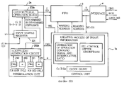
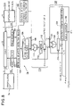
- FIG. 1 is a block diagram showing the configuration of a sampling frequency conversion apparatus that is an embodiment of the present invention.
- FIG. 2 is a diagram for explaining the contents of processing of an interpolative operation performed by a basic sampling frequency conversion apparatus.
- FIG. 3 is a diagram for explaining the contents of processing of an interpolative operation accompanied by double over-sampling based on zero point insertion.
- FIG. 4 is a diagram for explaining the contents of processing for an even cycle in an interpolative operation accompanied by double over-sampling based on zero point insertion and the contents of processing for an odd cycle therein.
- FIG. 5 is a diagram for explaining the contents of processing for an even cycle of an interpolative operation adopted by the embodiment and the contents of processing for an odd cycle thereof.
- FIG. 6 is a diagram showing interpolative coefficients to be used to calculate interpolated samples for the even cycle in the embodiment.
- FIG. 7 is a diagram showing interpolative coefficients used to calculate interpolated samples for the odd cycle in the embodiment.
- FIG. 8 is a block diagram showing the detailed configuration of a control unit 1 a provided in the embodiment.
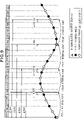
- FIG. 9 is a diagram showing an example of operation of the embodiment.
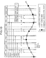
- FIG. 10 is a diagram showing an example of operation of the embodiment.
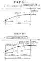
- FIGS. 11( a ) and 11 ( b ) are a diagram for explaining the fact that a regular coefficient generation circuit can be employed in the embodiment.
- FIG. 12 is a block diagram showing the configuration of a basic sampling frequency conversion apparatus.
- FIG. 13 is a diagram showing an example of operation of the basic sampling frequency conversion apparatus.
- FIG. 14 is a diagram for explaining a method of generating interpolative coefficients in the basic sampling frequency conversion apparatus.
- FIG. 15 is a diagram for explaining in detail a method of generating interpolative coefficients in the basic sampling frequency conversion apparatus.
- FIG. 16 is a diagram showing a method of identifying an interval, in which interpolative coefficients are present, and a linear interpolation method for the interpolative coefficients in the basic sampling frequency conversion apparatus.
- FIG. 17 is a diagram for explaining updating process of phase information performed in the basic sampling frequency conversion apparatus.
- FIG. 18 is a diagram for explaining an error in an interpolative operation occurring in the basic sampling frequency conversion apparatus.
- FIG. 12 is a block diagram showing an example of the configuration of a basic type of a sampling frequency conversion apparatus.
- the basic sampling frequency conversion apparatus is a device that performs an interpolative operation on samples x of a first sampling frequency f 1 (input sampling frequency) outputted from the device in the preceding stage, thus converts the samples x into interpolated samples y of a second sampling frequency f 2 (output sampling frequency) which the device in the succeeding stage requests, and outputs the samples y.
- the sampling frequency conversion apparatus includes a control unit 1 that controls the whole of the apparatus, an interpolation unit 2 , a first-in first-out (FIFO) 3 formed with a RAM or the like, and an interface 4 .
- a control unit 1 that controls the whole of the apparatus
- an interpolation unit 2 that controls the whole of the apparatus
- a first-in first-out (FIFO) 3 formed with a RAM or the like
- an interface 4 As shown in FIG. 12 , the sampling frequency conversion apparatus includes a control unit 1 that controls the whole of the apparatus, an interpolation unit 2 , a first-in first-out (FIFO) 3 formed with a RAM or the like, and an interface 4 .
- FIFO first-in first-out
- the input samples x of the first sampling frequency f 1 are fed from the device in a stage preceding the sampling frequency conversion apparatus.
- the interpolation unit 2 performs an interpolative operation on a sequence of a predetermined number of input samples x, which have been inputted previously, under the control of the control unit 1 , thus generates interpolated samples y of the second sampling frequency f 2 which the succeeding device requests, and outputs the interpolated samples y together with a writing request signal WE.
- the control unit 1 updates a writing address, which is fed to the FIFO 3 , responsively to the output of the writing request signal WE.
- the FIFO 3 is a first-in first-out buffer that sequentially stores the interpolated samples y, which are fed from the interpolation unit 2 together with the writing request signal WE, under the control of the control unit 1 , that reads out the stored samples y sequentially from oldest ones responsively to a reading request signal RE from the interface 4 , and that feeds the samples y as a sequence of interpolated samples z to the interface 4 .
- the interface 4 outputs the reading request signal RE to each of the FIFO 3 and the control unit 1 according to a word clock LRCK sent from the device in the succeeding stage.
- the control unit 1 updates a reading address fed to the FIFO 3 , and extends control so that the oldest one of the interpolated samples y that have not been read will be outputted from the FIFO 3 .
- the interface 4 receives the samples z read from the FIFO 3 responsively to the output of the reading request signal RE to the control unit 1 .
- the interface 4 then converts the received samples z into a serial bit string SDO, and outputs the bit string SDO synchronously with a bit clock BCK fed from the device in the succeeding stage.
- the word clock LRCK is a clock having the same frequency as the second sampling frequency f 2 requested by the device in the succeeding stage.
- FIG. 13 shows the contents of an interpolative operation performed by the interpolation unit 2 .
- black-circle marks indicate the input samples x fed to the interpolation unit 2
- void-triangle marks indicate the interpolated samples y to be generated by the interpolation unit 2 .
- the first sampling frequency f 1 is 48 kHz
- the second sampling frequency f 2 is 22.05 kHz.
- the interpolation unit 2 includes, as shown in FIG. 12 , an input sample register 201 , a coefficient generation circuit 202 , and a convolutional operation block 203 .
- the input sample register 201 is a shift register of, for example, N steps (where N denotes a predetermined integer).
- the input samples x of the first sampling frequency f 1 are sequentially fetched with a clock ⁇ 1 having the same frequency as the first sampling frequency f 1 .
- an operation request signal CRQ requesting the interpolative operation and an interpolative ratio ⁇ are fed from the control unit 1 .
- the interpolative ratio ⁇ refers to the phases at sampling points of the interpolated samples y to be generated by the interpolation unit 2 .
- the interpolation unit 2 obtains the interpolated sample y by performing the interpolative operation.
- the interpolative ratio ⁇ signifies at what position on a time base between the sampling point for the sample x[i ⁇ m] and the sampling point for the sample x [i ⁇ m+i] the sampling point for the interpolated sample y that should be obtained through the interpolative operation is located. Specifically, the interpolative ratio ⁇ signifies that the sampling point for the interpolated sample y is located to lead the sampling point for the sample x[i ⁇ m] in the input sample register 201 by an ⁇ cycle (one cycle is 1/f 1 ).
- the coefficient generation circuit 202 has a sampling function table, which lists function values at a plurality of points of a sampling function that is an impulse response of an ideal low-pass filter, stored therein ( FIG. 14 shows part of the points as “points of a known sampling function”). When a peak point of the sampling function is, as shown in FIG. 14 and FIG.
- the interpolative ratio ⁇ is, for example, data represented by 12 bits
- a time resolution for the sampling points of the interpolated samples y determined with the interpolative ratio ⁇ is a quotient of a period of 1/48 kHz divided by 4096.
- the sampling function values were listed in the sampling function table, a memory capacity required to store the values in the sampling function table would be enormous. This is not advantageous.
- FIG. 16 is a diagram for explaining the calculating method by taking an interpolative coefficient h[m] for instance.
- one interpolative coefficient h[m] would assume any of sampling function values within an interval of 1/48 kHz. Consequently, thirty-two sampling function values by which the interval of 1/48 kHz is divided into 32 intervals are listed per one interpolative coefficient h[m] in the sampling function table.
- the interpolative coefficient h[m] For calculation of the interpolative coefficient h[m], first, in whichever of the thirty-two intervals the interpolative coefficient h[m] to be obtained is present is identified based on six high-order bits of the 12-bit interpolative ratio ⁇ . Two sampling function values at both limits of the identified interval are read from the sampling function table. Thereafter, based on the six low-order bits of the 12-bit interpolative ratio ⁇ , linear interpolation is performed using the two read sampling function values in order to calculate the interpolative coefficient h[m].
- the control unit 1 therefore executes the updating process of the phase information P synchronously with a clock ⁇ m having the same frequency as the first sampling frequency f 1 .
- the aforesaid operation request signal CRQ and interpolative ratio ⁇ are generated in the process of the updating process of the position information P.
- FIG. 17 is a diagram showing the process of the updating process of the phase information P to be performed by the control unit 1 .
- an up-and-down direction is a time base.
- FIG. 17 shows a scene where the phase information P is updated synchronously with the clock ⁇ m.
- the phase information P When the phase information P is decremented by 1 synchronously with the clock ⁇ m, the phase information P duty gets smaller than 1.
- the control unit 1 sends the operation request signal CRQ to the interpolation unit 2 , and sends a decimal part of the phase information P as the interpolative ratio ⁇ to the interpolation unit 2 .
- This causes the interpolation unit 2 to generate the interpolative coefficient string h[k] (k 0 to N ⁇ 1) associated with the interpolative ratio ⁇ according to the aforesaid method.
- the operation request signal CRQ and interpolative ratio ⁇ are sent to the interpolation unit 2 at a temporal density inversely proportional to the conversional ratio ⁇ .
- the interpolated samples y juxtaposed while being interspaced by a ⁇ cycle are sequentially generated by the interpolation unit 2 .
- the interpolated samples y are sent to the device in the succeeding stage via the FIFO 3 and interface 4 .
- the foregoing sampling frequency conversion apparatus is supposed to meet the prerequisite that the frequency of a word clock LRCK to be fed from the device in the succeeding stage is the same as the second sampling frequency f 2 .
- the conversional ratio ⁇ may be fixed to f 1 /f 2 .
- jitter unavoidably occurs in the word clock LRCK.
- the control unit 1 performs so-called phase-locked loop (PLL) control for the purpose of absorbing the jitter of the word clock LRCK and preventing occurrence of the overflow or underflow of the FIFO 3 .
- PLL phase-locked loop
- the control unit 1 monitors a residual quantity of interpolated samples y that have not been read from the FIFO 3 , and increases or decreases a sample input speed for the FIFO 3 according to a variation in the residual quantity so that the residual quantity will be retained at an appropriate range.
- the control unit 1 increases the conversional ratio ⁇ so as to decrease the temporal density (namely to increase an interval) at which each operation command signal CRQ is sequentially generated, and thus decreases the sample input speed for the FIFO 3 .
- the conversional ratio ⁇ is decreased to increase the temporal density (namely to decrease an interval) at which each operation command signal CRQ is successively generated.
- the sample input speed for the FIFO 3 is increased.
- the input speed of the interpolated samples y from the interpolation unit 2 to the FIFO 3 follows the frequency of the word clock LRCK, and the residual quantity of interpolated samples y that have not been read from the FIFO 3 is retained within the appropriate range.
- the sampling frequency conversion apparatus may be used for sampling frequency conversion from the input sampling frequency to the output sampling frequency f 2 that is identical to or very close to the input sampling frequency f 1 of the input samples x.
- the frequency of a word clock LRCK to be sent from the succeeding device to the sampling frequency conversion apparatus may get higher than the sampling frequency f 1 for the input samples x due to an adverse effect of jitter.
- the device in the succeeding stage is designed to receive and process the interpolated samples y of 48 kHz.
- the conversional ratio ⁇ is smaller than 1, the phase information P becomes smaller than 1 within a certain sampling cycle ( 1/48 kHz).
- the operation command signal CRQ may be generated, and a result of addition of ⁇ 1 to the phase information P may be negative within the next sampling cycle.
- the sampling frequency conversion apparatus even when the jitter of the word clock LRCK is little, if the output sampling frequency requested by the device in the succeeding stage is equal to or larger than the input sampling frequency of input samples, the sampling frequency cannot be converted without occurrence of the error in the interpolative operation.
- FIG. 1 is a block diagram showing the configuration of a sampling frequency conversion apparatus in accordance with an embodiment of the present invention.
- a FIFO 3 and an interface 4 are identical to those contained in the basic sampling frequency conversion apparatus shown in FIG. 12 .
- the control unit 1 and interpolation unit 2 contained in the basic sampling frequency conversion apparatus shown in FIG. 12 are replaced with a control unit 1 a and an interpolation unit 2 a respectively.
- the features of the present embodiment lie in the improvements concerning the control unit 1 a and the interpolation unit 2 a which are described below.
- Improvement 1 the interpolation unit 2 a performs double over-sampling based on nominal zero-point insertion when calculating interpolated samples y by performing an interpolative operation using an original sequence of input samples (hereinafter, an input sample string) fed from a device in a preceding stage.
- Improvement 2 the control unit 1 a updates positional information P synchronously with a main clock ⁇ m whose frequency is a double of the sampling frequency f 1 for input samples x fed from the device in the preceding device.
- interpolation unit 2 a will be detailed while being centered on the improvement 1 , and the control unit 1 a will then be detailed while being centered on the improvement 2 .
- a method of performing double over-sampling may be conceivably applied to samples x of a sampling frequency of 48 kHz fed from a device in a preceding stage so that the sampling frequency for a sample string to be used for the interpolative operation is made higher than the original sampling frequency for an input sample string is conceivable.
- a zero point is inserted to each pair of twenty-two input samples x [ 21 ] to x[ 0 ] that have been fed up to a current time point, and decimation processing (low-pass filter processing) is performed on the resultant input samples in order to obtain an oversampled sequence of input samples x′[ 43 ] to x′[ 0 ] of forty-four input samples for which the sampling frequency f 1 is set to 96 kHz.
- an interpolative operation for obtaining interpolated samples y is to convolute a function value string of a sampling function, which represents an impulse response of an ideal low-pass filter, to an input sample string
- the interpolative operation fills the role of decimation processing (low-pass filter processing). Consequently, zero-point insertion for double over-sampling and decimation processing can be omitted.
- a method of inserting a zero point to each pair of twenty-two input samples x[ 21 ] to x[ 0 ] of 48 kHz in order to produce forty-four input samples x′[ 43 ] to x′[ 0 ] of 96 kHz, and performing an interpolative operation on the forty-four input samples in order to calculate the interpolated sample y is conceivable.
- the order of the interpolative operation is doubled to be forty-four-th.
- a processing load therefor is imposed on the interpolation unit 2 a.
- the calculation is performed as mentioned below.
- FIG. 4 shows the contents of processing to be performed in a case where input samples x are sequentially fed from a device in a preceding stage in cycles of 1/48 kHz, zero-point insertion is actually performed on the original input sample string, and an oversampled input sample string of forty-four samples obtained after zero-point insertion is used to perform a 44th-order interpolative operation in cycles of 1/96 kHz.
- FIG. 4 shows the contents of processing to be performed in a case where input samples x are sequentially fed from a device in a preceding stage in cycles of 1/48 kHz, zero-point insertion is actually performed on the original input sample string, and an oversampled input sample string of forty-four samples obtained after zero-point insertion is used to perform a 44th-order interpolative operation in cycles of 1/96 kHz.
- Interpolative coefficients h[ 0 ], h[ 1 ], etc., h[ 42 ], and h[ 43 ] for a 44th-order interpolative operation are convoluted to the interpolative-operation input sample string x′[ 43 ] to x′[ 0 ].
- the samples x′[ 42 ], x′[ 40 ], etc., and x′[ 0 ] that are zero points are multiplied by odd-numbered interpolative coefficients h[ 1 ], h[ 3 ], etc., and h[ 43 ] respectively.
- the results of the multiplication are all zeroes.
- the samples x′[ 43 ], x′[ 41 ], etc., and x′[ 1 ] that are not zero points are the original input samples x[ 21 ] to x[ 0 ] of 48 kHz, and are multiplied by even-numbered interpolative coefficients h[ 0 ], h[ 2 ], etc., and h[ 42 ] respectively.
- the interpolative-operation input sample string x′[ 43 ] to x′[ 0 ] is shifted by one sample.
- the content of the trailing (oldest) sample x′[ 0 ] (in this case, a zero point) is removed, and a zero point is assigned to the leading (latest) sample x[ 43 ].
- the contents of the samples x′[ 42 ], x′[ 40 ], etc., and x′[ 0 ] are the original input samples x[ 21 ] to x[ 0 ], and the contents of the samples x′[ 43 ], x′[ 41 ], etc., and x′[ 1 ] are zero points.
- the interpolative coefficients h[ 43 ], h[ 42 ], etc., h[ 1 ], and h[ 0 ] for a 44th-order interpolative operation are convoluted to the interpolative-operation input sample string x′[ 43 ] to x′[ 0 ].
- the samples x′[ 43 ], x′[ 41 ], etc., and x[ 1 ] that are zero points are multiplied by the even-numbered interpolative coefficients h[ 0 ], h[ 2 ], etc., and h[ 42 ] respectively.
- the results of the multiplication are all zeroes.
- the samples x′[ 42 ], x′[ 40 ], etc., and x′[ 0 ] that are not zero points are the original input samples x[ 21 ] to x[ 0 ] of 48 kHz, and are multiplied by the odd-numbered interpolative coefficients h[ 1 ], h[ 3 ], etc., and h[ 43 ] respectively.
- a difference between the first-half 1/96 kHz cycle and the second-half 1/96 Hz cycle lies in a point that the interpolative coefficients to be used for multiplication of the original input samples of 48 kHz in the first-half 1/96 kHz cycle are even-numbered interpolative coefficients, but the interpolative coefficients to be used in the second-half 1/96 kHz cycle are odd-numbered interpolative coefficients.
- an interpolative operation is performed on original input samples according to the method shown in FIG. 5 .
- the input sample register 201 shown in FIG. 1 is, similarly to that included in the basic structure, caused to update the stored contents thereof (interpolative-operation input sample string) synchronously with a clock having the same frequency as the sampling frequency f 1 for the input samples x.
- a sampling cycle of 1/48 kHz during which an interpolative-operation input sample string of the same contents is held in the input sample register 201 is divided into a first-half 1/96 kHz cycle (hereinafter an even cycle) and a second-half 1/96 kHz cycle (hereinafter an odd cycle).
- an advantage identical to the advantage to be provided when double over-sampling based on zero-point insertion is performed on an input sample string x[i ⁇ k] (k 0 to N ⁇ 1), and interpolated samples y are calculated by performing an interpolative operation of an order that is a multiple of an original order.
- An operation command signal CRQ and an interpolative ratio ⁇ are generated in the course of the updating process of the phase information P.
- whether the timing of generating the operation command signal CRQ and interpolative ratio ⁇ belongs to the even cycle or odd cycle has to be distinguished. Therefore, the control unit 1 a counts the main clock ⁇ m, and outputs a 1-bit odd/even instruction signal O/E, which is 0 for the even cycle and 1 for the odd cycle, to the interpolation unit 2 a.
- the interpolation unit 2 a includes two registers 210 and 211 for holding the operation command signal CRQ, and two registers 220 and 221 for holding the interpolative ratio ⁇ as phase information.
- the registers 210 and 220 are temporary storages for the even cycle
- the registers 211 and 221 are temporary storages for the odd cycle.
- the operation command signal CRQ and interpolative ratio ⁇ outputted from the control unit 1 a in the even cycle where the odd/even instruction signal O/E is 0 are held in the registers 210 and 220 respectively.
- the operation command signal CRQ and interpolative ratio ⁇ outputted from the control unit 1 a in the odd cycle where the odd/even instruction signal O/E is 1 are held in the registers 211 and 221 respectively.
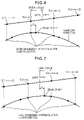
- FIG. 6 is a diagram showing a method of generating the interpolative coefficients.
- the interpolative coefficients are twenty-two even-numbered interpolative coefficients out of forty-four interpolative coefficients by which forty-four samples including virtual zero points are multiplied.
- FIG. 7 is a diagram showing a method of generating interpolative coefficients.
- the interpolative coefficients are twenty-two odd-numbered interpolative coefficients out of the forty-four interpolative coefficients by which the forty-four samples including virtual zero points are multiplied.
- the interpolated samples y may be calculated at any timing within the sampling cycle of 1/48 kHz.
- the interpolated samples y may be calculated at any timing within the sampling cycle of 1/48 kHz.
- the operation command signal CRQ and interpolative ratio ⁇ may be generated.
- the interpolation unit 2 a sequentially calculates the interpolated samples y in the even cycle within the sampling cycle of 1/48 kHz, and sequentially calculates the interpolated samples y in the odd cycle.
- the interpolation unit 2 a has been detailed so far.
- the inventive sampling frequency conversion apparatus is designed for applying an interpolative operation to input samples x having an input sampling frequency f 1 so as to compute interpolated samples y having an output sampling frequency f 2 which is specified by a succeeding device, and for outputting the interpolated samples y to the succeeding device.
- an input sample register 201 stores a predetermined number of input samples x as an original sequence of input samples for the interpolative operation.
- a coefficient generating part 202 a prepares a first sequence of interpolative coefficients corresponding to an oversampled sequence of input samples which are obtained by inserting nominal input samples of zero values to the input samples stored in the input sample register 201 , and generates a second sequence of interpolative coefficients which are extracted from the first sequence of the interpolative coefficients and which correspond to the original sequence of the input samples x.
- a convolutional operation part 203 a convolutes the second sequence of the interpolative coefficients with the original sequence of the input samples x so as to output the interpolated sample y.
- a control part 1 a operates in synchronization with a main clock ⁇ m having a frequency 2 f 1 twice as high as the input sampling frequency f 1 of the input samples x, for updating phase information ⁇ indicating a phase relation between the original sequence of the input samples x and a sequence of interpolated samples y to be generated, and generates an operation command signal CRQ instructing the interpolative operation for generating the interpolated sample y when the updated phase information ⁇ satisfies a predetermined condition.
- the input sample register 201 operates in synchronization with a frequency identical to the input sampling frequency f 1 of the input samples, for sequentially fetching the input samples x and storing N number of newest ones of the fetched input samples x as the original sequence of the input samples x for the interpolative operation.
- an even cycle operation command register 210 operates in synchronization with the main clock for storing the operation command signal CRQ when the same is generated in an even cycle of the main clock
- an even cycle phase information register 220 stores the phase information ⁇ associated with the operation command signal CRQ generated in the even cycle of the main clock
- an odd cycle operation command register 211 operates in synchronization with the main clock for storing the operation command signal CRQ when the same is generated in an odd cycle of the main clock
- an odd cycle phase information register 221 stores the phase information ⁇ associated with the operation command signal CREQ generated in the odd cycle of the main clock.
- the coefficient generating part 202 a operates when the operation command signal CRQ is stored in the even cycle operation command register 210 for performing an even interpolative coefficient generation process such as to generate the second sequence of the interpolative coefficients composed of N number of even interpolative coefficients which are extracted from the first sequence of 2N number of the interpolative coefficients which correspond to the oversampled sequence of 2N number of input samples such that the second sequence of the interpolative coefficients has the phase relation relative to the original sequence of the input samples x as indicated by the phase information ⁇ stored in the even cycle phase information register 220 .
- the coefficient generating part 202 a operates when the operation command signal CRQ is stored in the odd cycle operation command register 211 for performing an odd interpolative coefficient generation process such as to generate the second sequence of the interpolative coefficients composed of N number of odd interpolative coefficients which are extracted from the first sequence of 2N number of the interpolative coefficients corresponding to the oversampled sequence of 2N number of input samples such that the second sequence of the interpolative coefficients has the phase relation relative to the original sequence of the input samples as indicated by the phase information ⁇ stored in the odd cycle phase information register 221 .
- the coefficient generating part 202 a operates when the operation command signal CRQ is stored in both the even cycle operation command register 210 and the odd cycle operation command register 211 for performing both the even interpolative coefficient generation process and the odd interpolative coefficient generation process.
- the convolutional operation part 203 a operates each time the second sequence of the N number of the interpolative coefficients are generated by the coefficient generating part 202 a for performing a convolutional operation of the second sequence of N number of the coefficients and the original sequence of the N number of the input samples x to output the interpolated sample y.
- the coefficient generating part 202 a prepares the first sequence of the interpolative coefficients corresponding to the oversampled sequence of input samples which are obtained by inserting nominal input samples of zero values to the input samples x stored in the input sample register 201 so that the oversampled sequence of the input samples has an oversampling frequency twice as high of the input sampling frequency f 1 , such that each cycle of the input sampling frequency f 1 is divided into an even cycle and an odd cycle in correspondence to each cycle of the oversampling frequency 2 f 1 , and such that the first sequence of the interpolative coefficients contains even interpolative coefficients and odd interpolative coefficients corresponding to even cycles and odd cycles of the oversampling frequency 2 f 1 .
- the coefficient generating part 202 a operates at an even cycle for generating the second sequence of the even interpolative coefficients which are extracted from the first sequence of the interpolative coefficients, and operates at an odd cycle for generating the second sequence of the odd interpolative coefficients which are extracted from the first sequence of the interpolative coefficients.
- the convolutional operation part 2 a operates at the even cycle for convoluting the second sequence of the even interpolative coefficients with the original sequence of the input samples x so as to output the interpolated sample y, and operates at the odd cycle for convoluting the second sequence of the odd interpolative coefficients with the original sequence of the input samples x so as to output the interpolated sample y.
- the coefficient generating part 202 a prepares the first sequence of the interpolative coefficients which are twice as many as the number of input samples x contained in the original sequence of the input samples stored in the input sample register 201 .
- a write pointer 101 is a circuit that increments a writing address responsively to the output of a writing request signal WE from the interpolation unit 2 a , and feeds the writing address to the FIFO 3 .
- the interpolation unit 2 a outputs the interpolated sample y together with the writing request signal WE, the interpolated sample y sent from the interpolation unit 2 a is written in an area in the FIFO 3 designated with the writing address outputted from the write pointer 101 .
- a read pointer 102 sequentially increments a reading address in response to a reading request signal RE sent from the interface 4 , and feeds the reading address to the FIFO 3 .
- the reading address designates the oldest one of the interpolated samples y that have not been read and remain in the FIFO 3 .
- An interpolated sample y designated with the reading address is read from the FIFO 3 in response to the reading request signal RE, and fed to the interface 4 .
- a residual quantity detection block 103 is a circuit that detects a difference between a writing address generated by the write pointer 101 and a reading address generated by the read pointer 102 , that is, the residual quantity of interpolated samples y that have not been read and remain in the FIFO 3 at a current time point.
- a jitter correction value table 104 is a table associating residual quantities of interpolated samples y with jitter correction values, and outputs a jitter correction value associated with the residual quantity detected by the residual quantity detection block 103 .
- the jitter correction value is used to correct a conversional ratio ⁇ that determines a temporal density or interval at which each operation command signal CRQ is sequentially generated.
- the interval of CRQ is an inverse of temporal density of CRQ.
- the residual quantities falling within an appropriate range are associated with a jitter correction value that is 0.
- a larger value is associated with a jitter correction value that is larger in a negative direction.
- a smaller value is associated with a jitter correction value that is larger in a positive direction.
- a residual quantity increase/decrease detection circuit 105 is a circuit that detects an abrupt change in the residual quantity detected by the residual quantity detection block 103 .
- a selector 106 selects and outputs a jitter correction value outputted from the jitter correction value table 104 . Otherwise, the selector 106 selects and outputs 0 as the jitter correction value.
- a frequency correction block 110 is a circuit that corrects a conversional ratio ⁇ according to a jitter correction value, and includes an adder 111 , a limiter 112 , and a latch 113 .
- a clock ⁇ a is fed to the latch 113 .
- the clock ⁇ a is faster than the main clock ⁇ m, and has a frequency of, for example, 9 MHz.
- a value fm/f 2 calculated by dividing the frequency fm of the main clock ⁇ m by the post-conversion sampling frequency f 2 is set as an initial value of the conversional ratio ⁇ in the latch 113 .
- the latch 113 updates the conversional ratio ⁇ , which is fed from the adder 111 through the limiter 112 , every time the clock ⁇ a is fed.
- the adder 111 adds the jitter correction value, which is fed from the selector 106 , to the conversional ratio ⁇ outputted from the latch 113 , and outputs a resultant value. If the conversional ratio ⁇ outputted from the adder 111 falls outside an appropriate range, the limiter 112 fills the role of confining the conversional ratio ⁇ to the appropriate range. According to the configuration, when the jitter correction value of 0 is outputted from the selector 106 , the conversional ratio ⁇ outputted from the latch 113 does not change.
- the conversional ratio ⁇ outputted from the latch 113 decreases along with the passage of time.
- the conversional ratio ⁇ outputted from the latch 113 increases along with the passage of time.
- a temporal gradient of the decrease in the conversional ratio ⁇ or a temporal gradient of the increase therein gets larger as the absolute value of the jitter correction value gets larger.
- a phase information update block 120 is a circuit that updates the phase information P synchronously with the main clock ⁇ , and that generates the operation command signal CRQ at a temporal density, which is inversely proportional to the conversional ratio ⁇ , in the course of updating.
- the phase information update block 120 includes a selector 121 , an adder 122 , a latch 123 , and an operation command generator 124 .
- the selector 121 When the operation command signal CRQ is driven to an inactive level, the selector 121 outputs ⁇ 1 to the adder 122 .
- the selector 121 outputs data, which is calculated by subtracting 1 from the conversional ratio ⁇ fed from the frequency correction block 110 , to the adder 122 .
- the adder 122 is a circuit that adds data, which is fed via the selector 121 , to the phase information P held in the latch 123 so as to update the phase information P.
- the latch 123 is a circuit that holds the phase information P outputted from the adder 122 every time the main clock ⁇ m is fed.
- the operation command generator 124 drives the operation command signal CRQ to the inactive level.
- the operation command generator 124 drives the operation command signal CRQ to the active level during a period equivalent to one cycle of the clock ⁇ m.
- the operation command signal CRQ is driven to the inactive level, and ⁇ 1 is fed to the adder 122 via the selector 121 . Consequently, the phase information P outputted from the latch 123 with every generation of the main clock ⁇ m is decremented by one.
- the phase information P gets smaller than 1, the operation command signal CRQ is driven to the active level and the data calculated by subtracting 1 from the conversional ratio ⁇ is fed to the adder 122 via the selector 121 . Therefore, the phase information P increases by ⁇ 1. Consequently, the operation command signal CRQ is driven to the active level at a temporal density that is inversely proportional to the conversional ratio ⁇ .
- a clock counter 130 is a 1-bit counter that reverses the odd/even instruction signal O/E with every generation of the main clock ⁇ m.
- the odd/even instruction signal O/E is set to 1. What is obtained by adding the odd/even instruction signal O/E as the most significant bit to a bit string of a decimal part of the phase information P is regarded as the interpolative ratio ⁇ .
- the interpolative ratio ⁇ is fed together with the operation command signal CRQ to the interpolation unit 2 a .
- the configuration of the control unit 1 a has been detailed so far.
- an interface 4 receives a word clock LRCK having the same frequency f 2 as the output sampling frequency f 2 specified by the succeeding device, and transmits the interpolated samples y successively fed from the convolutional operation part 203 a to the succeeding device in synchronization with the word clock LRCK.
- the control part 1 a controls an interval of the operation command signals CRQ which are successively generated each time the updated phase information a satisfies the predetermined condition so as to allow the interval of the operation command signals CRQ to follow the frequency of the word clock f 2 .
- a first-in first-out buffer 3 sequentially stores the interpolated samples y outputted from the convolutional operation part 203 a , and sequentially reads and outputs the interpolated samples y from the old ones stored in the first-in first-out buffer 3 in response to the word clock LRCK.
- the control part 1 a includes a residual quantity detecting part 103 for detecting a residual quantity of the interpolated samples y that have not been read from the first-in first-out buffer 3 , and controls on the basis of the residual quantity detected by the residual quantity detecting part 103 so as to allow the interval of the operation command signals CRQ to follow the frequency of the word clock LRCK.
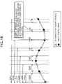
- FIG. 9 and FIG. 10 show examples of the operation of the present embodiment.
- the frequency f 2 of the word clock LRCK to be fed from the device in the succeeding stage is 22.05 kHz.
- the residual quantity of interpolated samples y in the FIFO 3 is detected by the residual quantity detection block 103 .
- control is extended to increase the conversional ratio ⁇ , decrease the temporal density at which the operation command signal CRQ is generated, and lower the input speed for the interpolated samples y from the interpolation unit 2 a to the FIFO 3 .
- control is extended to decrease the conversional ratio ⁇ , increase the temporal density at which the operation command signal CRQ is generated, and raise the input speed for the interpolated samples y from the interpolation unit 2 a to the FIFO 3 .
- update of the phase information P and generation of the operation command signal CRQ based on the result of the update are performed synchronously with the clock ⁇ m of the frequency fm of 96 kHz.
- the operation command signal CRQ may therefore be generated in the even cycle of the clock ⁇ m or may be generated in the odd cycle.
- the phase information P gets smaller than 1, and the operation command signal CRQ is generated.
- the interpolative ratio ⁇ becomes negative. An interpolative operation therefore causes an error. However, in the present embodiment, the error in the interpolative operation will not occur.
- the frequency f 2 of the word clock LRCK is 59.07 kHz
- the residual quantity of interpolated samples y in the FIFO 3 is confined to the appropriate range. Sampling frequency conversion is performed with the conversional ratio ⁇ set to 1.625.
- the interpolated samples y of 59.07 kHz resulting from the sampling frequency conversion are sent to the device in the succeeding stage via the FIFO 3 and interface 4 .
- the phase information P gets smaller than 1.
- the operation command signal CRQ is generated.
- sampling frequency conversion to a sampling frequency identical to the sampling frequency for input samples can be achieved without occurrence of an error in an interpolative operation.
- sampling frequency conversion to a frequency that is equal to or smaller than a double of the sampling frequency for input samples and that is higher than the sampling frequency for the input samples can be achieved.
- the coefficient generation circuit 202 employed in the basic sampling frequency conversion apparatus can be used as the coefficient generation circuit 202 a as it is. Referring to FIG. 11 , the advantage will be described below.
- FIG. 11( a ) shows a range of an interpolative coefficient h[m] by which a sample x[i ⁇ m] immediately preceding a sampling point for the interpolated sample y is multiplied during an interpolative operation.
- function values within an interval having a time length of 1/48 kHz on the left-hand side (negative side) of a peak point of a sampling function are generated as the interpolative coefficient h[m].
- the coefficient generation circuit 202 When the interpolative ratio ⁇ is 12-bit data, the coefficient generation circuit 202 generates a value, which may assume any value ranging from 0 to 4095 and which is associated with the value of the interpolative ratio ⁇ , out of function values of points into which the interval of 1/48 kHz is divided.
- FIG. 11( b ) shows ranges of interpolative coefficients h[ 2 m ] and h[ 2 m+ 1] by which a sample x[i ⁇ m] immediately preceding a sampling point for the interpolated sample y is multiplied during an interpolative operation.
- the even-numbered interpolative coefficient h[ 2 m ] is generated, and the sample x[i ⁇ m] is multiplied by the interpolative coefficient h[ 2 m ].
- the odd-numbered interpolative coefficient h[ 2 m+ 1] is generated, and the sample x[i ⁇ m] is multiplied by the interpolative coefficient.
- the coefficient generation circuit 202 employed in the basic sampling frequency conversion apparatus can be used as the coefficient generation circuit 202 a as it is.
- a clock ⁇ 1 to be fed to the input sample register 201 may be produced by halving the frequency of the main clock ⁇ m.
- a period during which the clock ⁇ 1 has an H level is regarded as the even cycle of the main clock ⁇ m, and a period during which the clock ⁇ 1 has an L level is regarded as the odd cycle.
- the clock ⁇ 1 may be substituted for the odd/even instruction signal O/E. According to this mode, the clock counter 130 for producing the odd/even instruction signal O/E can be excluded.
- the interpolative ratio ⁇ that is part (a decimal part) of the phase information P is sent to the interpolation unit 2 a in order to cause the interpolation unit 2 a to perform an interpolative operation.
- the operation command signal CRQ is generated, since an integral part of the phase information P is 0, the whole of the phase information P can be sent to the interpolation unit 2 a without any problem.
- the operation command signal CRQ when the phase information P gets smaller than 1, the operation command signal CRQ is generated.
- the phase information P falls below a predetermined value larger than 1, the operation command signal CRQ may be generated. Namely, when the fact that the phase relationship between the interpolative-operation input sample string and the interpolated samples y meets a predetermined condition is detected based on the phase information P, the operation command signal CRQ should be generated.
- the interface 4 receives the word clock LRCK having the same frequency as a sampling frequency requested by a device in a succeeding stage, and calculated interpolated samples are transmitted to the device in the succeeding stage synchronously with the word clock LRCK.
- the sampling frequency conversion apparatus may be designed so that: a sampling frequency requested by the device in the succeeding stage may be sensed through, for example, negotiation prior to the initiation of communication without reception of the word clock LRCK; and interpolated samples having the sampling frequency may be calculated using input samples x, and sent to the device in the succeeding stage.
Landscapes
- Transmission Systems Not Characterized By The Medium Used For Transmission (AREA)
- Complex Calculations (AREA)
Applications Claiming Priority (2)
| Application Number | Priority Date | Filing Date | Title |
|---|---|---|---|
| JP2007012076A JP4386079B2 (ja) | 2007-01-22 | 2007-01-22 | サンプリング周波数変換装置 |
| JP2007-012076 | 2007-01-22 |
Publications (2)
| Publication Number | Publication Date |
|---|---|
| US20090002208A1 US20090002208A1 (en) | 2009-01-01 |
| US7609181B2 true US7609181B2 (en) | 2009-10-27 |
Family
ID=39704702
Family Applications (1)
| Application Number | Title | Priority Date | Filing Date |
|---|---|---|---|
| US12/009,736 Expired - Fee Related US7609181B2 (en) | 2007-01-22 | 2008-01-22 | Sampling frequency conversion apparatus |
Country Status (3)
| Country | Link |
|---|---|
| US (1) | US7609181B2 (zh) |
| JP (1) | JP4386079B2 (zh) |
| CN (1) | CN101232277B (zh) |
Cited By (2)
| Publication number | Priority date | Publication date | Assignee | Title |
|---|---|---|---|---|
| US20070121971A1 (en) * | 2005-11-30 | 2007-05-31 | Takanobu Mukaide | Audio mixing device and audio mixing method |
| US20080114825A1 (en) * | 2006-09-11 | 2008-05-15 | Kabushiki Kaisha Toshiba | Digital signal processing apparatus and digital signal processing method |
Families Citing this family (2)
| Publication number | Priority date | Publication date | Assignee | Title |
|---|---|---|---|---|
| JP6107994B1 (ja) * | 2016-03-08 | 2017-04-05 | Nttエレクトロニクス株式会社 | データ処理装置、データ処理方法及び通信装置 |
| CN109614148B (zh) * | 2018-12-11 | 2020-10-02 | 中科驭数(北京)科技有限公司 | 数据逻辑运算方法、监测方法及装置 |
Citations (6)
| Publication number | Priority date | Publication date | Assignee | Title |
|---|---|---|---|---|
| JP2002158561A (ja) | 2000-11-20 | 2002-05-31 | Ando Electric Co Ltd | Firフィルタ及びそのデータ処理方法 |
| US6636165B2 (en) * | 2001-02-06 | 2003-10-21 | Rohde & Schwarz Gmbh & Co. Kg | Device and method for conversion of sampling rate |
| US7061409B1 (en) * | 2005-02-07 | 2006-06-13 | Nokia Corporation | Techniques for sample rate conversion |
| US20060188052A1 (en) | 2005-02-24 | 2006-08-24 | Yamaha Corporation | Data transmission controller and sampling frequency converter |
| JP2006238044A (ja) | 2005-02-24 | 2006-09-07 | Yamaha Corp | 伝送制御装置およびサンプリング周波数変換装置 |
| JP2006261812A (ja) | 2005-03-15 | 2006-09-28 | Yamaha Corp | 伝送制御装置およびサンプリング周波数変換装置 |
Family Cites Families (2)
| Publication number | Priority date | Publication date | Assignee | Title |
|---|---|---|---|---|
| EP0957579A1 (en) * | 1998-05-15 | 1999-11-17 | Deutsche Thomson-Brandt Gmbh | Method and apparatus for sampling-rate conversion of audio signals |
| WO2003044950A1 (en) * | 2001-11-19 | 2003-05-30 | Koninklijke Philips Electronics N.V. | Time discrete filter comprising upsampling, sampling rate conversion and downsampling stages |
-
2007
- 2007-01-22 JP JP2007012076A patent/JP4386079B2/ja not_active Expired - Fee Related
-
2008
- 2008-01-22 CN CN2008100043711A patent/CN101232277B/zh not_active Expired - Fee Related
- 2008-01-22 US US12/009,736 patent/US7609181B2/en not_active Expired - Fee Related
Patent Citations (7)
| Publication number | Priority date | Publication date | Assignee | Title |
|---|---|---|---|---|
| JP2002158561A (ja) | 2000-11-20 | 2002-05-31 | Ando Electric Co Ltd | Firフィルタ及びそのデータ処理方法 |
| US6889239B2 (en) | 2000-11-20 | 2005-05-03 | Yokogawa Electric Corporation | Digital filter and data processing method thereof |
| US6636165B2 (en) * | 2001-02-06 | 2003-10-21 | Rohde & Schwarz Gmbh & Co. Kg | Device and method for conversion of sampling rate |
| US7061409B1 (en) * | 2005-02-07 | 2006-06-13 | Nokia Corporation | Techniques for sample rate conversion |
| US20060188052A1 (en) | 2005-02-24 | 2006-08-24 | Yamaha Corporation | Data transmission controller and sampling frequency converter |
| JP2006238044A (ja) | 2005-02-24 | 2006-09-07 | Yamaha Corp | 伝送制御装置およびサンプリング周波数変換装置 |
| JP2006261812A (ja) | 2005-03-15 | 2006-09-28 | Yamaha Corp | 伝送制御装置およびサンプリング周波数変換装置 |
Non-Patent Citations (1)
| Title |
|---|
| Japanese Patent Office: Office Action, "Notice of Reasons for Refusal" for Patent Application No. 2007-012076, dated Mar. 3, 2009, (4 pgs.). |
Cited By (3)
| Publication number | Priority date | Publication date | Assignee | Title |
|---|---|---|---|---|
| US20070121971A1 (en) * | 2005-11-30 | 2007-05-31 | Takanobu Mukaide | Audio mixing device and audio mixing method |
| US20080114825A1 (en) * | 2006-09-11 | 2008-05-15 | Kabushiki Kaisha Toshiba | Digital signal processing apparatus and digital signal processing method |
| US8032575B2 (en) * | 2006-09-11 | 2011-10-04 | Kabushiki Kaisha Toshiba | Digital signal processing apparatus and digital signal processing method |
Also Published As
| Publication number | Publication date |
|---|---|
| CN101232277B (zh) | 2010-06-02 |
| JP4386079B2 (ja) | 2009-12-16 |
| CN101232277A (zh) | 2008-07-30 |
| US20090002208A1 (en) | 2009-01-01 |
| JP2008178049A (ja) | 2008-07-31 |
Similar Documents
| Publication | Publication Date | Title |
|---|---|---|
| JP2986745B2 (ja) | 複合位相濾波器とこれを用いたタイミング誤差補償装置及びその方法 | |
| US5471411A (en) | Interpolation filter with reduced set of filter coefficients | |
| US7719446B2 (en) | Method and apparatus for computing interpolation factors in sample rate conversion systems | |
| JPH08510100A (ja) | デジタル的にサンプルされた信号の再サンプリング同期装置 | |
| US7408485B1 (en) | Asynchronous sampling rate converter and method for audio DAC | |
| JP2001298368A (ja) | 圧縮方法及び装置、伸長方法及び装置、圧縮伸長システム、記録媒体 | |
| US7619546B2 (en) | Asynchronous sample rate conversion using a digital simulation of an analog filter | |
| JPH10200594A (ja) | ディジタル復調器におけるシンボルタイミング復元回路 | |
| US7609181B2 (en) | Sampling frequency conversion apparatus | |
| JPH10190759A (ja) | ディジタル復調器におけるタイミング補間器 | |
| JP2548210B2 (ja) | 時間軸補正装置 | |
| KR20160033916A (ko) | 샘플링 레이트 컨버터 및 그 방법 | |
| US7570727B2 (en) | Data transmission controller and sampling frequency converter | |
| CN100521532C (zh) | 数据传输控制和采样频率转换器 | |
| CN109976660B (zh) | 基于线性插值的任意信号采样率重构方法和数据采样系统 | |
| US6263036B1 (en) | Asynchronous signal input apparatus and sampling frequency conversion apparatus | |
| US7813566B2 (en) | Data processing apparatus and data processing method | |
| JP2600821B2 (ja) | 標本化周波数変換装置 | |
| CN102403985A (zh) | 采样频率转换器 | |
| US7680220B2 (en) | Numerical phase detector with interpolated values | |
| JP4488496B2 (ja) | 信号処理方法および信号処理装置 | |
| JP5573901B2 (ja) | 標本化レート変換装置 | |
| JP2001136073A (ja) | 圧縮方法及び装置、圧縮伸長システム、記録媒体 | |
| US5815419A (en) | Data interpolating circuit | |
| US7456762B1 (en) | Scaling of sampling position in sample rate converter |
Legal Events
| Date | Code | Title | Description |
|---|---|---|---|
| AS | Assignment |
Owner name: YAMAHA CORPORATION, JAPAN Free format text: ASSIGNMENT OF ASSIGNORS INTEREST;ASSIGNOR:NISHIOKA, NAOTOSHI;REEL/FRAME:020447/0957 Effective date: 20080110 |
|
| STCF | Information on status: patent grant |
Free format text: PATENTED CASE |
|
| FEPP | Fee payment procedure |
Free format text: PAYOR NUMBER ASSIGNED (ORIGINAL EVENT CODE: ASPN); ENTITY STATUS OF PATENT OWNER: LARGE ENTITY |
|
| FPAY | Fee payment |
Year of fee payment: 4 |
|
| FPAY | Fee payment |
Year of fee payment: 8 |
|
| FEPP | Fee payment procedure |
Free format text: MAINTENANCE FEE REMINDER MAILED (ORIGINAL EVENT CODE: REM.); ENTITY STATUS OF PATENT OWNER: LARGE ENTITY |
|
| LAPS | Lapse for failure to pay maintenance fees |
Free format text: PATENT EXPIRED FOR FAILURE TO PAY MAINTENANCE FEES (ORIGINAL EVENT CODE: EXP.); ENTITY STATUS OF PATENT OWNER: LARGE ENTITY |
|
| STCH | Information on status: patent discontinuation |
Free format text: PATENT EXPIRED DUE TO NONPAYMENT OF MAINTENANCE FEES UNDER 37 CFR 1.362 |
|
| FP | Lapsed due to failure to pay maintenance fee |
Effective date: 20211027 |