US7274224B2 - Semiconductor device and camera using same - Google Patents
Semiconductor device and camera using same Download PDFInfo
- Publication number
- US7274224B2 US7274224B2 US11/183,808 US18380805A US7274224B2 US 7274224 B2 US7274224 B2 US 7274224B2 US 18380805 A US18380805 A US 18380805A US 7274224 B2 US7274224 B2 US 7274224B2
- Authority
- US
- United States
- Prior art keywords
- semiconductor device
- source
- load
- transistor
- stage
- Prior art date
- Legal status (The legal status is an assumption and is not a legal conclusion. Google has not performed a legal analysis and makes no representation as to the accuracy of the status listed.)
- Expired - Fee Related, expires
Links
- 239000004065 semiconductor Substances 0.000 title claims abstract description 99
- 238000010586 diagram Methods 0.000 description 14
- 238000003384 imaging method Methods 0.000 description 14
- 230000000694 effects Effects 0.000 description 5
- 230000003247 decreasing effect Effects 0.000 description 4
- 230000003287 optical effect Effects 0.000 description 4
- 230000002093 peripheral effect Effects 0.000 description 4
- 230000003321 amplification Effects 0.000 description 3
- 230000001413 cellular effect Effects 0.000 description 3
- 238000003199 nucleic acid amplification method Methods 0.000 description 3
- 230000000630 rising effect Effects 0.000 description 3
- 238000012986 modification Methods 0.000 description 2
- 230000004048 modification Effects 0.000 description 2
- 230000008054 signal transmission Effects 0.000 description 2
- 230000007423 decrease Effects 0.000 description 1
- 229910044991 metal oxide Inorganic materials 0.000 description 1
- 150000004706 metal oxides Chemical class 0.000 description 1
- 238000000034 method Methods 0.000 description 1
Images


Classifications
-
- H—ELECTRICITY
- H03—ELECTRONIC CIRCUITRY
- H03F—AMPLIFIERS
- H03F1/00—Details of amplifiers with only discharge tubes, only semiconductor devices or only unspecified devices as amplifying elements
- H03F1/42—Modifications of amplifiers to extend the bandwidth
- H03F1/48—Modifications of amplifiers to extend the bandwidth of aperiodic amplifiers
- H03F1/483—Modifications of amplifiers to extend the bandwidth of aperiodic amplifiers with field-effect transistors
-
- H—ELECTRICITY
- H03—ELECTRONIC CIRCUITRY
- H03F—AMPLIFIERS
- H03F3/00—Amplifiers with only discharge tubes or only semiconductor devices as amplifying elements
- H03F3/34—DC amplifiers in which all stages are DC-coupled
- H03F3/343—DC amplifiers in which all stages are DC-coupled with semiconductor devices only
- H03F3/345—DC amplifiers in which all stages are DC-coupled with semiconductor devices only with field-effect devices
-
- H—ELECTRICITY
- H03—ELECTRONIC CIRCUITRY
- H03F—AMPLIFIERS
- H03F3/00—Amplifiers with only discharge tubes or only semiconductor devices as amplifying elements
- H03F3/50—Amplifiers in which input is applied to, or output is derived from, an impedance common to input and output circuits of the amplifying element, e.g. cathode follower
- H03F3/505—Amplifiers in which input is applied to, or output is derived from, an impedance common to input and output circuits of the amplifying element, e.g. cathode follower with field-effect devices
Definitions
- the present invention relates to a semiconductor device having a source-follower amplifier which is suitable as an amplifier device in a solid-state imaging device and the like, and a camera using the semiconductor device.
- CMOS metal-oxide semiconductor
- CCD charge-coupled device
- MOS metal-oxide semiconductor
- a frequency of a pixel signal is required to be high in order to consecutively capture a plurality of pictures.
- the frequency of the pixel signal may be low.
- a drive frequency is variable in a single CCD imaging device, it is desirable to minimize a frequency bandwidth of a source-follower amplifier in terms of noise reduction of the amplifier and power consumption reduction.
- FIG. 1 is a circuit diagram showing the conventional semiconductor device.
- a conventional semiconductor device 900 is comprised of source-follower amplifiers that form a three-stage structure.
- a source-follower amplifier in a first stage includes a driver transistor D 1 and a load transistor L 1
- a source-follower amplifier in a second stage includes a driver transistor D 2 and a load transistor L 2
- a source-follower amplifier in a third stage includes a driver transistor D 3 and a load transistor L 3 .
- the driver transistors D 1 , D 2 , and D 3 , and the load transistors L 1 , L 2 , and L 3 are MOS transistors.
- Drains of the driver transistors D 1 , D 2 , and D 3 in the source-follower amplifiers in the respective stages are connected to a power supply terminal VDD.
- Sources of the load transistors L 1 , L 2 , and L 3 in the source-follower amplifiers in the respective stages are connected to a ground terminal GND.
- the source of the driver transistor D 1 in the source-follower amplifier in the first stage is connected to the drain of the load transistor L 1 and also to a gate of the driver transistor D 2 in the source-follower amplifier in the second stage.
- a gate of the driver transistor D 1 is connected to an input terminal Vin to which a pixel signal is inputted in capturing moving pictures and still pictures.
- the source of the driver transistor D 2 in the source-follower amplifier in the second stage is connected to the drain of the load transistor L 2 and also to a gate of the driver transistor D 3 in the source-follower amplifier in the third stage.
- the source of the driver transistor D 3 in the source-follower amplifier in the third stage is connected to the drain of the load transistor L 3 and also to an output terminal Vout from which the pixel signal is outputted to the outside.
- a gate of the load transistor L 1 in the source-follower amplifier in the first stage is connected to the ground terminal GND, while gates of the load transistors L 2 and L 3 in the source-follower amplifiers in the second and third stages are applied with a same bias voltage LG that can vary to achieve a desirable frequency bandwidth of the signal inputted into the input terminal Vin. This enables the frequency bandwidth and the amount of power consumption to be consecutively changed by varying the bias voltage LG.
- the load capacitance C includes an input capacitance of the driver transistor in the next stage, a wiring capacitance, and the like.
- the source-follower amplifier in the final stage is connected to an external circuit thereby increasing its load capacitance more than load capacitances in other stages.
- an operating point of the output voltage Vo of the source-follower amplifier depends on a resistance ratio between the driver transistor D 1 and the load transistor L 1 .
- the source-follower amplifiers are used in a multi-stage structure in a signal outputting unit to reduce an output impedance.
- the equation (3) shows that the consumption current can be changed by varying the gate bias voltage.
- the equation (2) shows that the frequency bandwidth can be changed by changing the consumption current thereby varying the operating point Vo and eventually varying the transconductance. In this case, both the gain and the operating point are changed, and the amount of change can vary within an acceptable range, but the amount of change is small as described further below with reference to FIGS. 2 to 5 so that the gain and the operating point can vary within a substantially wide range.
- linearity of input-output characteristics a linear region of the input-output characteristics is reduced when the operating point is too low or too high, but the operating point of the multi-stage amplifiers is generally getting lower gradually towards the latter stages, so that, when voltages applied to the gates of the load transistors in the latter stages can vary, it does not need to consider a limit of a linearity whose operating point is high.
- a limit of a linearity whose operating point is low can vary within a substantially wide range since the change of the operating point is small as described above. Therefore, the three-stage source-follower amplifiers, in which the frequency bandwidths are reduced, enable a reduction in the consumption current compared to the consumption current in the two-stage source-follower amplifiers.
- the transconductance of the driver transistor in the third stage is greater than the transconductance of the driver transistor in the second stage, that is, the frequency bandwidth of the calculated by the equation (2) is greater than that of the two-stage source-follower amplifiers, so that the consumption currents can be reduced for the amount of the resulting extra currents.
- the gate widths and the gate lengths of the respective driver transistors are 8 ⁇ m and 4 ⁇ m in the first stage, 80 ⁇ m and 4 ⁇ m in the second stage, and 800 ⁇ m and 4.5 ⁇ m in the third stage, respectively, while the gate widths and the gate lengths of the respective load transistors are 10 ⁇ m and 26 ⁇ m in the first stage, 110 ⁇ m and 10 ⁇ m in the second stage, and 150 ⁇ m and 10 ⁇ m in the third stage, respectively.
- FIG. 2 When the gate bias voltage LG applied to the load transistors in the second and third stages varies from ⁇ 5 V to 0 V, a linear region of input characteristics is shown in FIG. 2 , the consumption current in the second stage is shown in FIG. 3 , the consumption current in the third stage is shown in FIG. 4 , and a frequency decreased by 3 dB is shown in FIG. 5 .
- the frequency decreased by 3 dB is 43 MHz when the LG is ⁇ 5V, and 145 MHz when the LG is 0V.
- the consumption currents are 1 mA and 10 mA, respectively, and the gain and operating points vary within an acceptable range.
- the consumption current in the third stage is reduced from 5 mA to 1 mA in the same bandwidth as compared to the characteristics in the two-stage source-follower amplifiers.
- the conventional semiconductor device can adjust the frequency bandwidths and the consumption currents in the latter stages, but cannot do so in the initial stage, which fails to adjust the frequency bandwidths and the consumption currents in all stages.
- the conventional semiconductor device cannot properly transmit a pixel signal when the frequency of the pixel signal is increased to capture moving pictures by the increased number of pixels.
- the frequency bandwidth in the initial stage has previously been adjusted to a high frequency to capture moving pictures by the increased number of pixels, a lot of the consumption currents are wasted in the source-follower amplifier in the initial stage in capturing moving pictures by the usual number of pixels and in capturing still pictures.
- a semiconductor device includes: an initial-stage source-follower amplifier including a first driver transistor, and a first load transistor that is connected to the first driver transistor and driven variably depending on a signal inputted to the first driver transistor; and a final-stage source-follower amplifier including a second driver transistor, and a load circuit that is connected to the second driver transistor and driven variably depending on a signal outputted from the second driver transistor, wherein a gate of the first load transistor is applied with a variable bias voltage, and the load circuit is applied with a variable control voltage to vary a dynamic resistance value of the load circuit.
- the load circuit may be a second load transistor, and a gate of the second load transistor is applied with a variable bias voltage to vary a resistance value of the second load transistor.
- the load circuit may include a plurality of second load transistors that are connected in parallel to each other, and respective gates of the second load transistors are applied with respective variable bias voltages to vary respective resistance values of the second load transistors.
- the load circuit may include a second load transistor and a constant current circuit that are connected in parallel to one another, a gate of the second load transistor is applied with a variable bias voltage to vary a resistance value of the second load transistor, and the constant current circuit is applied with a variable control voltage to vary a dynamic resistance value of the constant current circuit.
- the constant current circuit has good constant current characteristics, so that increase of its conductance is restricted more than that of the load transistors in the source-follower amplifiers, which enables to restrain the gain reduction.
- the load circuit may be placed outside of the semiconductor device.
- the constant current circuit may include a constant current device and a resistance device that is connected to the constant current device, and the constant current device may be applied with the variable control voltage to vary the dynamic resistance value of the constant current circuit.
- the constant current device may be a bipolar transistor.
- the constant current device may be a MOS transistor.
- the resistance device may include a plurality of resistance elements, and a resistance value of the resistance device varies by selecting one of the resistance elements to be used.
- the load circuit may be a constant current circuit, and the constant current circuit is applied with a variable control voltage to vary a dynamic resistance value of the constant current circuit.
- the constant current circuit has good constant current characteristics, so that increase of its conductance is restricted more than that of the load transistors in the source-follower amplifiers, which enables to restrain the gain reduction.
- the semiconductor device may further include a source-follower amplifier that drives the final-stage source-follower amplifier variably depending on a signal outputted from the first driver transistor, the source-follower amplifier being placed between the initial-stage source-follower amplifier and the final-stage source-follower amplifier.
- the present invention can be implemented as a camera including the above-described semiconductor device.
- the semiconductor device of the present invention it is possible to prevent the conventional problems such as failing of proper pixel signal transmission and wasting of consumption currents in the source-follower amplifier in the initial stage in capturing moving pictures by the usual number of pixels or still pictures, and also possible to appropriately adjust the frequency bandwidths and the consumption currents to be increased or reduced in the source-follower amplifiers in all stages by appropriately varying the bias voltages LG 1 and LG 2 .
- the present invention can appropriately cope with various situations from capture of high-quality moving pictures to capture of still pictures, so that the present invention is highly suitable for practical use in the present day when cellular telephones equipped with digital cameras are widely used.
- FIG. 1 is a circuit diagram showing a conventional semiconductor device
- FIG. 2 is a graph showing an output voltage when a bias voltage LG applied to gates of load transistors in source-follower amplifiers in second and third stages varies from ⁇ 5 V to 0 V, according to the semiconductor device 900 shown in FIG. 1 ;
- FIG. 3 is a graph showing consumption current in source-follower amplifier in the second stage according to the semiconductor device 900 shown in FIG. 1 ;
- FIG. 4 is a graph showing consumption current in source-follower amplifier in the third stage according to the semiconductor device 900 shown in FIG. 1 ;
- FIG. 5 is a graph showing a frequency decreased by 3 dB according to the semiconductor device 900 shown in FIG. 1 ;
- FIG. 6 is a circuit diagram showing a structure of a semiconductor device according to a first embodiment of the present invention.
- FIG. 7 is a circuit diagram showing a structure of a semiconductor device according to a second embodiment of the present invention.
- FIG. 8 is a circuit diagram showing a variation of the semiconductor device according to the second embodiment of the present invention.
- FIG. 9 is a circuit diagram showing a structure of a semiconductor device according to a third embodiment of the present invention.
- FIG. 10 is a circuit diagram showing a structure example of a resistance element shown in FIG. 9 ;
- FIG. 11 is a circuit diagram showing another structure example of the resistance element shown in FIG. 9 ;
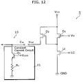
- FIG. 12 is a circuit diagram showing a structure of a semiconductor device according to a fourth embodiment of the present invention.
- FIG. 13 is a diagram showing a structure of a camera using the semiconductor devices according to the first to fourth embodiments.
- FIG. 6 is a circuit diagram showing a structure of a semiconductor device according to the first embodiment of the present invention. Note that the reference numerals in FIG. 1 are assigned to identical elements in FIG. 6 .
- a semiconductor device 1 according to the first embodiment of the present invention is comprised of source-follower amplifiers that form a two-stage structure.
- a source-follower amplifier in a first stage includes a driver transistor D 1 and a load transistor L 1
- a source-follower amplifier in a second stage includes a driver transistor D 2 and a load transistor L 2 .
- the driver transistors D 1 and D 2 and the load transistors L 1 and L 2 are MOS transistors.
- Drains of the driver transistors D 1 and D 2 in the source-follower amplifiers of the respective stages are connected to a power supply terminal VDD.
- Sources of the load transistors L 1 and L 2 in the source-follower amplifiers of the respective stages are connected to a ground terminal GND.
- the source of the driver transistor D 1 in the source-follower amplifier in the first stage is connected to the drain of the load transistor L 1 and also to a gate of the driver transistor D 2 in the source-follower amplifier in the second stage.
- a gate of the driver transistor D 1 is connected to an input terminal Vin to which a pixel signal is inputted in capturing moving pictures and still pictures.
- the source of the driver transistor D 2 in the source-follower amplifier in the second stage is connected to the drain of the load transistor L 2 and also to an output terminal Vout.
- a gate of the load transistor L 1 is applied with a bias voltage LG 1 that can vary to achieve a desirable frequency bandwidth of the signal inputted into the input terminal Vin. Further, a gate of the load transistor L 2 is applied with a bias voltage LG 2 that can vary to achieve a desirable frequency bandwidth of the signal inputted into the input terminal Vin.
- the semiconductor device 1 differs from the conventional semiconductor device 900 , not only in that the source-follower amplifiers form the two-stage structure, not the three-stage structure, but also in that the bias voltage LG 1 of the load transistor in the source-follower amplifier in the initial stage can vary, and especially in that the bias voltages LG 1 and LG 2 of the load transistors L 1 and L 2 in the source-follower amplifiers in the initial and second stages can vary separately.
- the bias voltages LG 1 and LG 2 to be applied may be generated outside of the semiconductor device, or inside of the semiconductor device.
- the semiconductor device 1 it is possible to change the frequency bandwidth and the consumption current in the source-follower amplifier in the initial stage as well as in the source-follower amplifiers in the latter stages, thereby enabling to change the frequency bandwidths and the consumption currents in the source-follower amplifiers in all stages.
- the bias voltages LG 1 and LG 2 are increased to increase transconductance of the load transistors L 1 and L 2 , thereby increasing the frequency bandwidths and the consumption currents in the source-follower amplifiers in the first and second stages.
- the bias voltages LG 1 and LG 2 are reduced depending on a frequency of the moving picture, to reduce transconductance of the load transistors L 1 and L 2 , thereby reducing the frequency bandwidths and the consumption currents in the source-follower amplifiers in the first and second stages.
- the bias voltages LG 1 and LG 2 are further reduced depending on a transfer frequency of the still picture, to further reduce transconductance of the load transistors L 1 and L 2 , thereby further reducing the frequency bandwidths and the consumption currents in the source-follower amplifier in the first and second stages.
- LG 1 and LG 2 are preferably LG 1 ⁇ LG 2 .
- semiconductor device 1 it is possible to prevent the conventional problems such as failing of proper pixel signal transmission and wasting of consumption currents in the source-follower amplifier in the initial stage in capturing moving pictures by the usual number of pixels or still pictures, and is also possible to appropriately adjust the frequency bandwidths and the consumption currents to be increased or reduced in the source-follower amplifiers in all stages by appropriately varying the bias voltages LG 1 and LG 2 .
- the bias voltages of the load transistors L 1 and L 2 can vary separately, but it is also possible to vary the bias voltages with the same value since the load transistors L 1 and L 2 have the same tendency of increasing and reducing depending on the bandwidth.
- the semiconductor device 1 is composed of the source-follower amplifiers forming a two-stage structure, but the structure may have one stage, or three or more stages.
- FIG. 7 is a circuit diagram showing a structure of the semiconductor device according to the second embodiment of the present invention. Note that the reference numerals in FIGS. 1 and 6 are assigned to identical elements in FIG. 7 .
- a semiconductor device 2 of the second embodiment differs from the semiconductor device 1 of the first embodiment in that a source-follower amplifier in a second stage has a plurality of load transistors (two load transistors in FIG. 7 ). More specifically, load transistors in the source-follower amplifier in the second stage (final stage) are a load transistor L 2 a and a load transistor L 2 b that is connected in parallel to the load transistor L 2 a.
- the semiconductor device 2 is comprised of source-follower amplifiers that form a two-stage structure, and the load transistor L 2 b that is connected in parallel to the load transistor L 2 a in the source-follower amplifier in the second stage.
- a source-follower amplifier in a first stage includes a driver transistor D 1 and a load transistor L 1
- a source-follower amplifier in a second stage includes a driver transistor D 2 and load transistors L 2 a and L 2 b.
- Drains of the driver transistors D 1 and D 2 in the source-follower amplifiers of the respective stages are connected to a power supply terminal VDD.
- Sources of the load transistors L 1 , L 2 a , and L 2 b in the source-follower amplifiers of the respective stages are connected to a ground terminal GND.
- the source of the driver transistor D 1 in the source-follower amplifier in the first stage is connected to the drain of the load transistor L 1 and also to a gate of the driver transistor D 2 in the source-follower amplifier in the second stage.
- a gate of the driver transistor D 1 is connected to an input terminal Vin to which a pixel signal is inputted in capturing moving pictures and still pictures.
- the source of the driver transistor D 2 in the source-follower amplifier in the second stage is connected to the drains of the load transistors L 2 a and L 2 b , respectively, and also to an output terminal Vout from which the pixel signal is outputted to the outside.
- Gates of the load transistors L 1 and L 2 a are applied with a bias voltage LGa that can vary to achieve a desirable frequency bandwidth of the signal inputted into the input terminal Vin. Further, a gate of the load transistor L 2 b is applied with a bias voltage LGb that can vary to achieve a desirable frequency bandwidth of the signal inputted into the input terminal Vin.
- the semiconductor device 2 differs from the conventional semiconductor device 900 in that the source-follower amplifiers form the two-stage structure, that the load transistor L 2 b is added to be connected in parallel to the load transistor L 2 a in the source-follower amplifier in the second stage, that the load transistors L 1 and L 2 a in the source-follower amplifiers in the initial and second stages are applied with the same variable bias voltage LGa, and that the load transistors L 2 b is applied with a variable voltage that is different from the voltage applied to the load transistors in the initial and second stages.
- the semiconductor device 2 it is possible to change the frequency bandwidth and the consumption current in the source-follower amplifier in the initial stage as well as in the source-follower amplifiers in the latter stage, thereby enabling to adjust the frequency bandwidths and the consumption currents in the source-follower amplifiers in all stages.
- the second embodiment has described that the gates of the load transistors L 1 and L 2 are applied with the same variable bias voltage LGa, but it is also possible, as shown in FIG. 8 , to implement a semiconductor device 3 in which the gate of the load transistor L 1 is applied with a variable bias voltage LG 1 , while the gate of the load transistor L 2 a is applied with the variable bias voltage LGa.
- a semiconductor device 3 in which the gate of the load transistor L 1 is applied with a variable bias voltage LG 1 , while the gate of the load transistor L 2 a is applied with the variable bias voltage LGa.
- FIG. 9 is a circuit diagram showing a structure of the semiconductor device according to the third embodiment of the present invention. Note that the reference numerals in FIGS. 1 , 6 , 7 , 8 are assigned to identical elements in FIG. 9 .
- the second embodiment has described that the load of the driver transistor D 2 is adjusted by the load transistor L 2 b in the source-follower amplifier, but in a semiconductor device 4 according to the third embodiment, the load of the driver transistor D 2 is totally adjusted using a constant current circuit 11 in peripheral circuitry 10 that is externally connected to an output terminal Vout.
- the semiconductor device 4 is comprised of source-follower amplifiers that form a two-stage structure as the semiconductor device 1 of the first embodiment.
- the constant current circuit 11 in the peripheral circuitry 10 is comprised of a bipolar transistor Q 1 and a resistance element R 1 .
- a collector of the bipolar transistor Q 1 is connected to the output terminal Vout via an input terminal Cin.
- An emitter of the bipolar transistor Q 1 is connected to one end of the resistance element R 1 .
- the other end of the resistance element R 1 is connected to ground.
- a base of the bipolar transistor Q 1 is applied with a control voltage Vcont.
- the semiconductor device 4 by varying the bias voltage LG and the control voltage Vcont, it is possible to change the frequency bandwidth and the consumption current in the source-follower amplifier in the initial stage as well as in the source-follower amplifiers in the latter stage, thereby enabling to adjust the frequency bandwidths and the consumption currents in the source-follower amplifiers in all stages.
- a value of the resistance element R 1 in the constant current circuit 11 can vary, thereby changing the combined resistance value of the constant current circuit 11 .
- the resistance element R 1 may be comprised of n resistor elements including r 1 , r 2 , . . . , r n , and n switch transistors including SW 1 , SW 2 , . . . , SW n , so that the value of the resistance element R 1 can vary using a combination of appropriately switching on the switch transistors SW 1 to SW n .
- the resistance element R 1 may be comprised of n resistor elements including r 1 to rn, and a selector 12 , and the value of the resistance element R 1 can vary by appropriately selecting the resistor elements r 1 to rn.
- a value of the control voltage Vcont is constant, by varying the value of the resistance element R 1 , it is possible to change the frequency bandwidth and the consumption current in the source-follower amplifier in the initial stage as well as in the source-follower amplifiers in the latter stage, thereby enabling to adjust the frequency bandwidths and the consumption currents in the source-follower amplifiers in all stages. Furthermore, it is possible to change the consumption current in the source-follower amplifier in the second stage without changing transconductance of the load transistor L 2 a , thereby further reducing the combined resistance values of the load transistors L 2 a and the constant current circuit 11 , which results in still another effect of further improving falling edge characteristics of the signal, restricting the gain reduction more than that of the conventional semiconductor device 900 .
- FIG. 12 is a circuit diagram showing a structure of the semiconductor device according to the fourth embodiment of the present invention. Note that the reference numerals in FIGS. 1 , 6 , 7 , 8 and 9 are assigned to identical elements in FIG. 12 .
- the third embodiment has described that the load of the driver transistor D 2 is adjusted by the load transistor L 2 in the source-follower amplifier and the constant current circuit 11 out side of the source-follower amplifiers, but in a semiconductor device 5 according to the fourth embodiment, the load of the driver transistor D 2 is totally adjusted using the constant current circuit 11 in the peripheral circuitry 10 that is externally connected to an output terminal Vout.
- the semiconductor device 5 has a structure in which the load transistor L 2 in the semiconductor device 4 of the third embodiment is eliminated. More specifically, the semiconductor device 5 is comprised of a source-follower amplifier in a single stage, and a driver transistor D 2 that drives the source-follower amplifier variably depending on signals outputted from the driver transistor D 2 and that serves as another source-follower amplifier in a second stage.
- a constant current circuit 11 in peripheral circuitry 10 is comprised of a bipolar transistor Q 1 and a resistance element R 1 .
- a collector of the bipolar transistor Q 1 is connected to the output terminal Vout via an input terminal Cin.
- An emitter of the bipolar transistor Q 1 is connected to one end of the resistance element R 1 .
- the other end of the resistance element R 1 is connected to ground.
- a base of the bipolar transistor Q 1 is applied with a control voltage Vcont.
- the semiconductor device 5 by varying the bias voltage LG and the control voltage Vcont, it is possible to change the frequency bandwidth and the consumption current in the source-follower amplifier in the initial stage as well as in the source-follower amplifiers in the latter stage, thereby enabling to adjust the frequency bandwidths and the consumption currents in the source-follower amplifiers in all stages.
- a value of the resistance element R 1 of the constant current circuit 11 can vary, thereby changing combined resistance value of the constant current circuit 11 .
- semiconductor devices 1 to 5 may be respectively equipped in an electronic component such as an imaging device to form a camera including the electronic component, thereby realizing the same operations and effects as described for the semiconductor devices 1 to 5 .
- FIG. 13 shows a structure of a camera using the semiconductor devices according to the first and second embodiments.
- a camera 400 consists of a lens 401 for imaging an optical image of an object to an imaging device, an optical system 402 such as a mirror and a shutter for optical processing of the optical image transmitted through the lens 401 , a MOS transistor type imaging device 403 equipped with the above-described semiconductor device, a signal processing unit 410 , a timing control unit 411 , and the like.
- the timing control unit 411 consists of a CDS circuit 404 for taking a difference between signals of fieldthrough outputted from the MOS transistor type imaging device 403 and outputting signals, an OB clamping circuit 405 for detecting OB level signals outputted from the CDS circuit 404 , a GCA 406 for adjusting a gain which is a difference between an OB level and an effective pixel signal level, an ADC 407 for converting analog signals outputted from the GCA 406 into digital signals, and the like.
- the timing control unit 411 consists of a DSP 408 for performing signal processing for the digital signals outputted from the ADC 407 and controlling driving timings, and a TG 409 for generating various driving pulses at various timings in the MOS transistor type imaging device 403 under the control of the DSP 408 , and the like.
- the camera 400 having the above structure, it is possible to realize a camera expanding the bandwidth without increasing currents in capturing moving pictures, moreover narrowing the bandwidth and improving the amplification factor in capturing still pictures by the MOS type imaging device 403 equipped with the above-mentioned semiconductor device. This means that it is possible to realize a camera that enables to adjust the frequency bandwidths and the consumption currents to be increased or reduced in the source-follower amplifiers in all stages.
- the imaging device has described as the MOS type imaging device, but it may be a CCD type imaging device.
- the present invention is suited to be implemented as a semiconductor device having a source-follower amplifier and a camera using the semiconductor device, such as an imaging device, a digital still camera, a cellular telephone equipped with a camera, a camera built in a laptop computer, a camera unit connected to a data processing apparatus.
- a semiconductor device having a source-follower amplifier and a camera using the semiconductor device, such as an imaging device, a digital still camera, a cellular telephone equipped with a camera, a camera built in a laptop computer, a camera unit connected to a data processing apparatus.
Landscapes
- Engineering & Computer Science (AREA)
- Power Engineering (AREA)
- Transforming Light Signals Into Electric Signals (AREA)
- Solid State Image Pick-Up Elements (AREA)
- Amplifiers (AREA)
Applications Claiming Priority (2)
| Application Number | Priority Date | Filing Date | Title |
|---|---|---|---|
| JP2004221685A JP4520241B2 (ja) | 2004-07-29 | 2004-07-29 | 半導体装置およびカメラ |
| JP2004-221685 | 2004-07-29 |
Publications (2)
| Publication Number | Publication Date |
|---|---|
| US20060022708A1 US20060022708A1 (en) | 2006-02-02 |
| US7274224B2 true US7274224B2 (en) | 2007-09-25 |
Family
ID=35355286
Family Applications (1)
| Application Number | Title | Priority Date | Filing Date |
|---|---|---|---|
| US11/183,808 Expired - Fee Related US7274224B2 (en) | 2004-07-29 | 2005-07-19 | Semiconductor device and camera using same |
Country Status (4)
| Country | Link |
|---|---|
| US (1) | US7274224B2 (ko) |
| EP (1) | EP1622259A1 (ko) |
| JP (1) | JP4520241B2 (ko) |
| KR (1) | KR100719189B1 (ko) |
Cited By (1)
| Publication number | Priority date | Publication date | Assignee | Title |
|---|---|---|---|---|
| US20130147525A1 (en) * | 2011-05-11 | 2013-06-13 | Fuji Electric Co., Ltd. | Drive circuit for insulated gate switching element |
Families Citing this family (2)
| Publication number | Priority date | Publication date | Assignee | Title |
|---|---|---|---|---|
| JP4723994B2 (ja) | 2005-12-19 | 2011-07-13 | 株式会社東芝 | 固体撮像装置 |
| JP5206397B2 (ja) | 2008-02-19 | 2013-06-12 | 株式会社Jvcケンウッド | 液晶表示装置及び液晶表示装置の駆動方法 |
Citations (8)
| Publication number | Priority date | Publication date | Assignee | Title |
|---|---|---|---|---|
| JPS6058706A (ja) * | 1983-09-09 | 1985-04-04 | Sharp Corp | ソ−スフオロア回路 |
| US5241502A (en) * | 1990-08-09 | 1993-08-31 | Samsung Electronics Co., Ltd. | Data output buffer circuit with precharged bootstrap circuit |
| JPH09307093A (ja) | 1996-05-13 | 1997-11-28 | Nec Corp | 半導体装置 |
| EP0951142A2 (en) | 1998-04-14 | 1999-10-20 | Eastman Kodak Company | Cmos imager column buffer gain compensation circuit |
| US6100744A (en) * | 1997-09-04 | 2000-08-08 | Samsung Electronics Co., Ltd. | Integrated circuit devices having improved internal voltage generators which reduce timing skew in buffer circuits therein |
| US20030001632A1 (en) | 2001-06-28 | 2003-01-02 | Intel Corporation | Voltage buffer |
| US6525613B2 (en) * | 2001-05-25 | 2003-02-25 | Infineon Technologies Ag | Efficient current feedback buffer |
| US20060038903A1 (en) * | 2004-07-29 | 2006-02-23 | Ryoichi Nagayoshi | Semiconductor device and camera using same |
Family Cites Families (5)
| Publication number | Priority date | Publication date | Assignee | Title |
|---|---|---|---|---|
| JP2982353B2 (ja) * | 1991-03-19 | 1999-11-22 | ソニー株式会社 | 固体撮像装置 |
| JP3335365B2 (ja) * | 1991-05-22 | 2002-10-15 | ソニー株式会社 | 固体撮像装置 |
| JPH0670239A (ja) * | 1992-08-20 | 1994-03-11 | Matsushita Electron Corp | 固体撮像装置 |
| JP4243047B2 (ja) * | 2001-08-23 | 2009-03-25 | 富士フイルム株式会社 | Ccd出力回路およびccd出力方法 |
| KR100977253B1 (ko) * | 2003-12-30 | 2010-08-30 | 이상철 | 팬을 이용한 에어로 핀 단열시스템 |
-
2004
- 2004-07-29 JP JP2004221685A patent/JP4520241B2/ja not_active Expired - Fee Related
-
2005
- 2005-07-11 EP EP05014983A patent/EP1622259A1/en not_active Withdrawn
- 2005-07-19 US US11/183,808 patent/US7274224B2/en not_active Expired - Fee Related
- 2005-07-28 KR KR1020050068739A patent/KR100719189B1/ko not_active IP Right Cessation
Patent Citations (12)
| Publication number | Priority date | Publication date | Assignee | Title |
|---|---|---|---|---|
| JPS6058706A (ja) * | 1983-09-09 | 1985-04-04 | Sharp Corp | ソ−スフオロア回路 |
| US5241502A (en) * | 1990-08-09 | 1993-08-31 | Samsung Electronics Co., Ltd. | Data output buffer circuit with precharged bootstrap circuit |
| JPH09307093A (ja) | 1996-05-13 | 1997-11-28 | Nec Corp | 半導体装置 |
| JP2795314B2 (ja) | 1996-05-13 | 1998-09-10 | 日本電気株式会社 | 半導体装置 |
| US5905256A (en) | 1996-05-13 | 1999-05-18 | Nec Corporation | Imaging device including output amplifier circuit having variable GAIN BANDWIDTH PRODUCT |
| US6100744A (en) * | 1997-09-04 | 2000-08-08 | Samsung Electronics Co., Ltd. | Integrated circuit devices having improved internal voltage generators which reduce timing skew in buffer circuits therein |
| EP0951142A2 (en) | 1998-04-14 | 1999-10-20 | Eastman Kodak Company | Cmos imager column buffer gain compensation circuit |
| US6169430B1 (en) * | 1998-04-14 | 2001-01-02 | Eastman Kodak Company | CMOS imager column buffer gain compensation circuit |
| US6525613B2 (en) * | 2001-05-25 | 2003-02-25 | Infineon Technologies Ag | Efficient current feedback buffer |
| US20030001632A1 (en) | 2001-06-28 | 2003-01-02 | Intel Corporation | Voltage buffer |
| US6518817B2 (en) | 2001-06-28 | 2003-02-11 | Intel Corporation | Voltage buffer |
| US20060038903A1 (en) * | 2004-07-29 | 2006-02-23 | Ryoichi Nagayoshi | Semiconductor device and camera using same |
Non-Patent Citations (1)
| Title |
|---|
| Patent Abstracts of Japan, vol. 9, No. 189, (E-333), Aug. 6, 1985 & JP 60 058706 A (Sharp KK), Apr. 4, 1985 * whole document *. * |
Cited By (2)
| Publication number | Priority date | Publication date | Assignee | Title |
|---|---|---|---|---|
| US20130147525A1 (en) * | 2011-05-11 | 2013-06-13 | Fuji Electric Co., Ltd. | Drive circuit for insulated gate switching element |
| US9246474B2 (en) * | 2011-05-11 | 2016-01-26 | Fuji Electric Co., Ltd. | Drive circuit for insulated gate switching element |
Also Published As
| Publication number | Publication date |
|---|---|
| KR100719189B1 (ko) | 2007-05-16 |
| KR20060066612A (ko) | 2006-06-16 |
| EP1622259A1 (en) | 2006-02-01 |
| JP4520241B2 (ja) | 2010-08-04 |
| US20060022708A1 (en) | 2006-02-02 |
| JP2006042139A (ja) | 2006-02-09 |
Similar Documents
| Publication | Publication Date | Title |
|---|---|---|
| JP6369696B2 (ja) | 固体撮像装置及び撮像装置 | |
| US7030922B2 (en) | Image pickup apparatus which reduces noise generated in an amplifier transistor | |
| US6906586B2 (en) | Differential amplifier circuit used in solid-state image pickup apparatus, and arrangement that avoids influence of variations of integrated circuits in manufacture and the like | |
| US7282990B2 (en) | Operational amplifier for output buffer and signal processing circuit using the same | |
| US20060038903A1 (en) | Semiconductor device and camera using same | |
| US20070177313A1 (en) | Semiconductor integrated circuit device | |
| US4443717A (en) | High resolution fast diode clamped comparator | |
| US7274224B2 (en) | Semiconductor device and camera using same | |
| US7605853B2 (en) | Solid-state image sensing device and camera | |
| US7068090B2 (en) | Amplifier circuit | |
| KR100296451B1 (ko) | 개선된이득을가지는소오스팔로워회로및그것을이용한고체촬상장치의출력회로 | |
| JP3335365B2 (ja) | 固体撮像装置 | |
| JP2008124229A (ja) | 固体撮像素子 | |
| JPH10136266A (ja) | 固体撮像装置 | |
| US20070035648A1 (en) | Solid-state imaging apparatus | |
| JPH11205693A (ja) | 固体撮像装置 | |
| US7321245B2 (en) | Pipelined AD converter capable of switching current driving capabilities | |
| US7429893B2 (en) | Variable-gain amplifier and related method | |
| JP4797600B2 (ja) | 固体撮像素子の出力バッファ回路およびこれを用いた固体撮像装置 | |
| US20050057233A1 (en) | Current control circuit, semiconductor device and image pickup device | |
| EP0951142A2 (en) | Cmos imager column buffer gain compensation circuit | |
| JP2010148008A (ja) | 固体撮像装置 | |
| JP2002057946A (ja) | 固体撮像素子の出力回路 | |
| KR101438829B1 (ko) | 액츄에이터 드라이버 | |
| JP2007019691A (ja) | 固体撮像装置 |
Legal Events
| Date | Code | Title | Description |
|---|---|---|---|
| AS | Assignment |
Owner name: MATSUSHITA ELECTRIC INDUSTRIAL CO., LTD., JAPAN Free format text: ASSIGNMENT OF ASSIGNORS INTEREST;ASSIGNOR:NAGAYOSHI, RYOICHI;REEL/FRAME:016788/0590 Effective date: 20050705 |
|
| STCF | Information on status: patent grant |
Free format text: PATENTED CASE |
|
| FEPP | Fee payment procedure |
Free format text: PAYOR NUMBER ASSIGNED (ORIGINAL EVENT CODE: ASPN); ENTITY STATUS OF PATENT OWNER: LARGE ENTITY |
|
| FPAY | Fee payment |
Year of fee payment: 4 |
|
| FEPP | Fee payment procedure |
Free format text: PAYER NUMBER DE-ASSIGNED (ORIGINAL EVENT CODE: RMPN); ENTITY STATUS OF PATENT OWNER: LARGE ENTITY Free format text: PAYOR NUMBER ASSIGNED (ORIGINAL EVENT CODE: ASPN); ENTITY STATUS OF PATENT OWNER: LARGE ENTITY |
|
| FPAY | Fee payment |
Year of fee payment: 8 |
|
| FEPP | Fee payment procedure |
Free format text: MAINTENANCE FEE REMINDER MAILED (ORIGINAL EVENT CODE: REM.); ENTITY STATUS OF PATENT OWNER: LARGE ENTITY |
|
| LAPS | Lapse for failure to pay maintenance fees |
Free format text: PATENT EXPIRED FOR FAILURE TO PAY MAINTENANCE FEES (ORIGINAL EVENT CODE: EXP.); ENTITY STATUS OF PATENT OWNER: LARGE ENTITY |
|
| STCH | Information on status: patent discontinuation |
Free format text: PATENT EXPIRED DUE TO NONPAYMENT OF MAINTENANCE FEES UNDER 37 CFR 1.362 |
|
| FP | Lapsed due to failure to pay maintenance fee |
Effective date: 20190925 |