US7236903B2 - Test apparatus and control method - Google Patents
Test apparatus and control method Download PDFInfo
- Publication number
- US7236903B2 US7236903B2 US11/136,335 US13633505A US7236903B2 US 7236903 B2 US7236903 B2 US 7236903B2 US 13633505 A US13633505 A US 13633505A US 7236903 B2 US7236903 B2 US 7236903B2
- Authority
- US
- United States
- Prior art keywords
- signal sequence
- output
- expectation
- comparison
- electronic device
- Prior art date
- Legal status (The legal status is an assumption and is not a legal conclusion. Google has not performed a legal analysis and makes no representation as to the accuracy of the status listed.)
- Expired - Lifetime, expires
Links
Images


Classifications
-
- G—PHYSICS
- G01—MEASURING; TESTING
- G01R—MEASURING ELECTRIC VARIABLES; MEASURING MAGNETIC VARIABLES
- G01R31/00—Arrangements for testing electric properties; Arrangements for locating electric faults; Arrangements for electrical testing characterised by what is being tested not provided for elsewhere
- G01R31/28—Testing of electronic circuits, e.g. by signal tracer
- G01R31/317—Testing of digital circuits
- G01R31/3181—Functional testing
- G01R31/319—Tester hardware, i.e. output processing circuits
- G01R31/31917—Stimuli generation or application of test patterns to the device under test [DUT]
- G01R31/31928—Formatter
-
- G—PHYSICS
- G01—MEASURING; TESTING
- G01R—MEASURING ELECTRIC VARIABLES; MEASURING MAGNETIC VARIABLES
- G01R31/00—Arrangements for testing electric properties; Arrangements for locating electric faults; Arrangements for electrical testing characterised by what is being tested not provided for elsewhere
- G01R31/28—Testing of electronic circuits, e.g. by signal tracer
- G01R31/317—Testing of digital circuits
- G01R31/3181—Functional testing
- G01R31/31813—Test pattern generators
-
- G—PHYSICS
- G01—MEASURING; TESTING
- G01R—MEASURING ELECTRIC VARIABLES; MEASURING MAGNETIC VARIABLES
- G01R31/00—Arrangements for testing electric properties; Arrangements for locating electric faults; Arrangements for electrical testing characterised by what is being tested not provided for elsewhere
- G01R31/28—Testing of electronic circuits, e.g. by signal tracer
- G01R31/317—Testing of digital circuits
- G01R31/3181—Functional testing
- G01R31/319—Tester hardware, i.e. output processing circuits
- G01R31/31917—Stimuli generation or application of test patterns to the device under test [DUT]
Definitions
- the present invention relates to a testing device and a control method testing an electronic device.
- the present application also relates to the following application, the contents of which are incorporated herein by reference if applicable.
- testing device that inputs a test pattern to an electronic device and tests the electronic device by comparing an output signal sequence output from the electronic device in response to the test pattern and an expectation signal sequence expected to be output from the electronic device.
- the testing device cannot adequately test the electronic device when a gap in the timing between the output of the output signal sequence and the output of the expectation signal sequence is not uniform.
- a testing device that tests an electronic device.
- the testing device includes: a pattern generator operable to generate a test pattern to be supplied to the electronic device and an expectation signal sequence to be output from the electronic device when the test pattern is supplied to the electronic device; a comparison unit operable to compare an output signal sequence output from the electronic device according to the test pattern with the expectation signal sequence; an acquisition controlling unit operable to cause the comparison unit to start comparing the output signal sequence and the expectation signal sequence when detecting an output header, which indicates the start of a comparison between the output signal sequence and the expectation signal sequence using the comparison unit, from the output signal sequence; and a comparison result outputting unit operable to acquire a comparison result from the comparison unit according to an instruction from the acquisition controlling unit.
- the comparison unit may include: a first converter that converts the serial expectation signal sequence into a parallel signal sequence every a predetermined data size; a second converter that converts the serial output signal sequence into a parallel signal sequence every the predetermined data size; and an output header detector that detects the output header based on the comparison between the converted output signal sequence and the converted expectation signal sequence, and the acquisition controlling unit may detect the output header based on the comparison result from the output header detector.
- the acquisition controlling unit may stop the comparison performed in the comparison unit when the test by the test pattern is finished, and the comparison unit may acquire an expectation header showing an expected value of an output header corresponding to a next test following the test by the test pattern as the expectation signal sequence.
- the comparison result outputting unit may output a signal showing that the test by the test pattern is correct in a state where the comparison by the comparison unit has been stopped.
- the comparison unit may include: a first shift register that acquires the expectation signal sequence; a second shift register that acquires the output signal sequence; an output header detector that compares the output signal sequence acquired by the second shift register and the expectation signal sequence acquired by the first shift register using a predetermined plurality of stages of the shift registers when detecting the output header; and a comparator that compares the output signal sequence acquired by the second shift register and the expectation signal sequence acquired by the first shift register using one predetermined stage of each of the shift registers when having detected the output header.
- the acquisition controlling unit may stop acquiring the expectation signal sequence when detecting an expectation header to indicate the start of the expectation signal sequence from the first shift register, and resume acquiring the expectation signal sequence when detecting the output header from the second shift register.
- the acquisition controlling unit may decide correspondence between the output signal sequence and the expectation signal sequence acquired by the second shift register and the first shift register in order to detect the output header.
- the acquisition controlling unit may use all stages of the shift registers during detecting the output header and use some stages of the shift registers during comparing the output signal sequence and the expectation signal sequence.
- a control method controlling a testing device that tests an electronic device.
- the control method includes: generating a test pattern to be supplied to the electronic device and an expectation signal sequence to be output from the electronic device when the test pattern is supplied to the electronic device; and starting comparing an output signal sequence and the expectation signal sequence when detecting an output header, which indicates the start of a comparison between the output signal sequence and the expectation signal sequence using a comparison unit, from the output signal sequence.
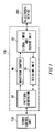
- FIG. 1 is a view exemplary showing a configuration of a testing device according to an embodiment of the present invention.
- FIG. 2 is a view exemplary showing a configuration of a deciding unit.
- FIG. 3 is a flowchart showing an operation of the deciding unit.
- FIGS. 4A and 4B are views exemplary showing signal sequences acquired by a first shift register and a second shift register.
- FIG. 1 is a view exemplary showing a configuration of a testing device 100 according to the present invention.
- the testing device 100 tests the electronic device 200 .
- the testing device 100 includes a pattern generator 50 , a waveform shaper 40 , a signal input and output unit 30 , and a deciding unit 20 .
- the pattern generator 50 generates a test pattern for testing the electronic device 200 .
- the pattern generator 50 receives test data that are used for testing the electronic device 200 from a tester control unit 150 provided outside, and generates the test pattern based on the test data.
- the tester control unit 150 is a computer such as a workstation.
- the pattern generator 50 generates an expectation signal sequence showing an expected value to be output from the electronic device when the test pattern is supplied to the electronic device 200 .
- the waveform shaper 40 receives and shapes the test pattern, and supplies the shaped test pattern to the signal input and output unit 30 at the desired timing.
- the signal input and output unit 30 supplies the received test pattern to the electronic device 200 , and receives an output signal sequence output from the electronic device 200 based on the test pattern. Moreover, the signal input and output unit 30 supplies the received output signal sequence to the deciding unit 20 .
- the deciding unit 20 decides the quality of the electronic device 200 based on the received output signal sequence. For example, the deciding unit 20 receives the expectation signal sequence from the pattern generator 50 , and decides the quality of the electronic device 200 by comparing the expectation signal sequence and the output signal sequence of the electronic device 200 . For example, when the electronic device 200 to be tested receives a plurality of commands and sequentially processes these commands, output timing is different from one another according to an internal operational state of the device, in some cases. In this case, it is necessary to correctly decide when the output signal sequence output from the electronic device 200 should begin to be compared with the expectation signal sequence. Thus, in the present embodiment, the deciding unit 20 starts comparing the output signal sequence and the expectation signal sequence following an output head when detecting the output head that is an output signal output from the electronic device corresponding to the start portion of the test pattern.
- FIG. 2 is a view exemplary showing a configuration of the deciding unit 20 .
- the deciding unit 20 has a comparison unit 210 , a comparison result outputting unit 230 , and an acquisition controlling unit 240 .
- the comparison unit 210 acquires the expectation signal sequence from the pattern generator 50 according to an instruction from the acquisition controlling unit 240 , and acquires the output signal sequence from the deciding unit 20 . Then, when the comparison unit 210 detects an output header showing the start of comparison between the expectation signal sequence and the output signal sequence, the comparison unit 210 sends that effect to the acquisition controlling unit 240 . For example, the comparison unit 210 detects the output header by comparing the output signal sequence with an expectation header showing the start of the expectation signal sequence. The acquisition controlling unit 240 sends an instruction to continue to acquire the expectation signal sequence to the comparison unit 210 , and sends an instruction to start the acquisition of a comparison result to the comparison result outputting unit 230 .
- the comparison unit 210 compares the expectation signal sequence received from an expectation signal sequence buffer 205 and the output signal sequence received from the signal input and output unit 30 , and sends the comparison result to the comparison result outputting unit 230 .
- the comparison result outputting unit 230 outputs the comparison result to the pattern generator 50 .
- the comparison result outputting unit 230 outputs a signal showing that a test by the test pattern is correct to the pattern generator 50 even in a state where the comparison by the comparison unit 210 is stopped.
- the comparison unit 210 includes the expectation signal sequence buffer 205 , a first shift register 214 , a second shift register 218 , a comparator 224 , and an output header detector 228 .
- the first shift register 214 acquires the expectation signal sequence from the expectation signal sequence buffer 205 , converts this serial sequence into a parallel sequence every a predetermined data size (for example, every eight stages that is all stages of the first shift register 214 ), and outputs the converted result to the output header detector 228 .
- the first shift register 214 outputs the value of some stages (for example, the most significant stage that is a predetermined one stage) of the first shift register 214 to the comparator 224 .
- the second shift register 218 acquires the output signal sequence from the signal input and output unit 30 , converts this serial sequence into a parallel sequence every a predetermined data size (for example, every eight stages), and outputs the converted result to the output header detector 228 . Moreover, the second shift register 218 outputs the value of the most significant stage that is one predetermined stage to the comparator 224 .
- the output header detector 228 compares the converted output signal sequence and the converted expectation signal sequence, detects the output header based on the comparison result, and sends the detected result to the acquisition controlling unit 240 .
- the acquisition controlling unit 240 sends an instruction to continue to output the expectation signal sequence to the expectation signal sequence buffer 205 .
- the expectation signal sequence buffer 205 sends the expectation signal sequence acquired from the pattern generator 50 to the first shift register 214 according to the instruction from the acquisition controlling unit 240 .
- the comparator 224 compares the values of the most significant stages of the first shift register 214 and the second shift register 218 , and sequentially sends the comparison results to the comparison result outputting unit 230 .
- the comparison unit 210 uses all stages of each shift register when detecting the output header, and uses some stages of each shift register when detecting truth of the output signal. In other words, the comparison unit 210 can select the number of stages to be used in each shift register corresponding to the detection of the output header or the decision of truth of the output signal.
- FIG. 3 is a flowchart showing an operation of the deciding unit 20 .
- the first shift register 214 acquires the expectation header and stops acquiring the expectation signal sequence (S 100 ).
- the second shift-register 218 acquires the output signal sequence (S 110 ).
- the output header detector 228 detects the output header (S 120 ). For example, the output header detector 228 compares the output signal sequence and the expectation signal sequence acquired by the second shift register 218 and the first shift register 214 and decides correspondence between the sequences in order to detect the output header. Alternatively, the output header detector 228 may decide that the output header has been detected when the output signal sequence corresponds to a predetermined pattern.
- the output header detector 228 may decide that the binary data completely correspond to each other to detect the output header.
- the expectation header is a binary data row and may have either of zero or one (for example, a don't care condition)
- the output header detector 228 may decide whether the output signal sequence corresponds to the expectation signal sequence with respect to the other data except for the don't care and detect the output header.
- the deciding unit 20 returns the process to the step S 110 .
- the first shift register 214 and the second shift register 218 respectively start acquiring the expectation signal sequence and the output signal sequence.
- the comparator 224 compares the output signal sequence and the expectation signal sequence (S 130 ).
- the deciding unit 20 decides whether the ongoing test by one test pattern has been finished (S 140 ). When it is decided that the test has not been finished (S 140 : NO), the deciding unit 20 returns the process to the step S 130 .
- the deciding unit 20 can synchronize an expectation signal and an output signal and adequately continue the test when the test is started or the test by one test pattern is finished.
- FIGS. 4A and 4B are views exemplary showing the signal sequences acquired by the first shift register 214 and the second shift register 218 .
- the horizontal direction of this drawing indicates time.
- the frames of broken lines showing the first shift register 214 and the second shift register 218 shows data respectively acquired by the first shift register 214 and the second shift register 218 .
- the first shift register 214 and the second shift register 218 have already acquired an expectation signal sequence 320 and an output signal sequence 322 and finished the process such as a comparison.
- the first shift register 214 acquires an expectation header 310 of an expectation signal sequence to be used for a new test following the test using the test pattern.
- the acquisition controlling unit 240 stops outputting the expectation signal sequence by the expectation signal sequence buffer 205 to stop the comparison performed in the comparator 224 .
- the acquisition controlling unit 240 decides whether the expectation header 310 has been acquired by comparing predetermined data and data acquired in the first shift register 214 .
- the acquisition controlling unit 240 may decide whether the expectation header 310 has been acquired by receiving timing information, at which the expectation header 310 is acquired, from an outside apparatus such as the pattern generator 50 .
- the output header detector 228 detects an output header showing the start of an output signal sequence from the second shift register 218 .
- the output header detector 228 can compare the second shift register 218 and the first shift register 214 to detect the output header.
- the acquisition controlling unit 240 resumes outputting the expectation signal sequence from the expectation signal sequence buffer 205 to cause the first shift register 214 to resume acquiring the expectation signal sequence of the next test. In this way, when the expectation header has been detected from the first shift register 214 , the acquisition controlling unit 240 can stop acquiring the expectation signal sequence until the output header is detected from the second shift register 218 .
- the deciding unit 20 of the testing device 100 can control acquisition timing of the expectation signal sequence to synchronize the output signal sequence and the expectation signal sequence and adequately compare these sequences.
Landscapes
- Engineering & Computer Science (AREA)
- General Engineering & Computer Science (AREA)
- Physics & Mathematics (AREA)
- General Physics & Mathematics (AREA)
- Tests Of Electronic Circuits (AREA)
Priority Applications (2)
| Application Number | Priority Date | Filing Date | Title |
|---|---|---|---|
| DE200610024932 DE102006024932A1 (de) | 2005-05-24 | 2006-05-22 | Prüfvorrichtung und Steuerverfahren |
| KR1020060046426A KR20060121742A (ko) | 2005-05-24 | 2006-05-24 | 시험 장치 및 제어 방법 |
Applications Claiming Priority (2)
| Application Number | Priority Date | Filing Date | Title |
|---|---|---|---|
| JP2004-064407 | 2004-03-08 | ||
| JP2004064407A JP4360944B2 (ja) | 2004-03-08 | 2004-03-08 | 試験装置及び制御方法 |
Publications (2)
| Publication Number | Publication Date |
|---|---|
| US20050270038A1 US20050270038A1 (en) | 2005-12-08 |
| US7236903B2 true US7236903B2 (en) | 2007-06-26 |
Family
ID=35030326
Family Applications (1)
| Application Number | Title | Priority Date | Filing Date |
|---|---|---|---|
| US11/136,335 Expired - Lifetime US7236903B2 (en) | 2004-03-08 | 2005-05-24 | Test apparatus and control method |
Country Status (2)
| Country | Link |
|---|---|
| US (1) | US7236903B2 (enExample) |
| JP (1) | JP4360944B2 (enExample) |
Cited By (2)
| Publication number | Priority date | Publication date | Assignee | Title |
|---|---|---|---|---|
| US20070094558A1 (en) * | 2005-10-24 | 2007-04-26 | Hon Hai Precision Industry Co., Ltd. | Apparatus and method for testing an IEEE1394 port |
| US8667346B2 (en) | 2010-07-29 | 2014-03-04 | Fujitsu Limited | Semiconductor integrated circuit device, method of controlling the semiconductor integrated circuit device and information processing system |
Families Citing this family (4)
| Publication number | Priority date | Publication date | Assignee | Title |
|---|---|---|---|---|
| JP4746510B2 (ja) * | 2006-02-21 | 2011-08-10 | 愛三工業株式会社 | 負荷駆動系の異常診断システムおよび燃料ポンプ制御システム |
| JP5113624B2 (ja) * | 2007-05-24 | 2013-01-09 | 株式会社アドバンテスト | 試験装置 |
| US20140355658A1 (en) * | 2013-05-30 | 2014-12-04 | Avago Technologies General Ip (Singapore) Pte. Ltd. | Modal PAM2/PAM4 Divide By N (Div-N) Automatic Correlation Engine (ACE) For A Receiver |
| CN115437345A (zh) * | 2022-08-15 | 2022-12-06 | 北京罗克维尔斯科技有限公司 | 一种测试车机端批量信号处理准确性的方法、装置及系统 |
Citations (2)
| Publication number | Priority date | Publication date | Assignee | Title |
|---|---|---|---|---|
| US20010034866A1 (en) * | 2000-01-14 | 2001-10-25 | Barry John Lee | Algorithmic test pattern generator, with built-in-self-test (BIST) capabilities, for functional testing of a circuit |
| US6453435B1 (en) * | 1998-12-29 | 2002-09-17 | Fujitsu Network Communications, Inc. | Method and apparatus for automated testing of circuit boards |
-
2004
- 2004-03-08 JP JP2004064407A patent/JP4360944B2/ja not_active Expired - Fee Related
-
2005
- 2005-05-24 US US11/136,335 patent/US7236903B2/en not_active Expired - Lifetime
Patent Citations (2)
| Publication number | Priority date | Publication date | Assignee | Title |
|---|---|---|---|---|
| US6453435B1 (en) * | 1998-12-29 | 2002-09-17 | Fujitsu Network Communications, Inc. | Method and apparatus for automated testing of circuit boards |
| US20010034866A1 (en) * | 2000-01-14 | 2001-10-25 | Barry John Lee | Algorithmic test pattern generator, with built-in-self-test (BIST) capabilities, for functional testing of a circuit |
Cited By (2)
| Publication number | Priority date | Publication date | Assignee | Title |
|---|---|---|---|---|
| US20070094558A1 (en) * | 2005-10-24 | 2007-04-26 | Hon Hai Precision Industry Co., Ltd. | Apparatus and method for testing an IEEE1394 port |
| US8667346B2 (en) | 2010-07-29 | 2014-03-04 | Fujitsu Limited | Semiconductor integrated circuit device, method of controlling the semiconductor integrated circuit device and information processing system |
Also Published As
| Publication number | Publication date |
|---|---|
| JP2005249736A (ja) | 2005-09-15 |
| JP4360944B2 (ja) | 2009-11-11 |
| US20050270038A1 (en) | 2005-12-08 |
Similar Documents
| Publication | Publication Date | Title |
|---|---|---|
| US8278961B2 (en) | Test apparatus and test method | |
| JP2004506204A (ja) | 高速データストリームの捕捉および評価 | |
| US6604058B2 (en) | Semiconductor device testing apparatus and method for testing semiconductor device | |
| US8299810B2 (en) | Test apparatus and electronic device | |
| US7236903B2 (en) | Test apparatus and control method | |
| US7235995B2 (en) | Test apparatus and testing method | |
| US8427188B2 (en) | Test apparatus | |
| US20020099993A1 (en) | Semiconductor testing apparatus and method | |
| US7299395B2 (en) | Test apparatus | |
| TWI634341B (zh) | 克服自動測試設備的時序約束衝突之設備及方法 | |
| US5570383A (en) | Timing hazard detector accelerator | |
| US20030128045A1 (en) | Apparatus and method for testing semiconductor storage device | |
| US6246971B1 (en) | Testing asynchronous circuits | |
| JP2006250940A (ja) | 圧縮データにおける誤り検出 | |
| US20100313091A1 (en) | Apparatus and method for testing semiconductor integrated circuit | |
| JPH102937A (ja) | Ic試験装置 | |
| KR20060121742A (ko) | 시험 장치 및 제어 방법 | |
| US6973395B2 (en) | Observation and/or failure inspection apparatus, method and program therefor | |
| US7092827B2 (en) | Edge placement accuracy of signals generated by test equipment | |
| JP3609780B2 (ja) | ジッタ測定装置及び方法、並びにこのジッタ測定装置を備えた半導体集積回路試験装置 | |
| JP2007515816A (ja) | 任意のテスト信号を使用するデジタルデータ信号のテスト | |
| US5191281A (en) | IC tester capable of changing strobe position in accordance with a predetermined reference signal | |
| KR101021095B1 (ko) | 위상제어루프의 지터 측정 방법, 장치 및 그 방법을 수행하기 위한 프로그램이 기록된 기록매체 | |
| JP2000149593A (ja) | Ic試験装置 | |
| JPH1048296A (ja) | Ic検査装置 |
Legal Events
| Date | Code | Title | Description |
|---|---|---|---|
| AS | Assignment |
Owner name: ADVANTEST CORPORATION, JAPAN Free format text: ASSIGNMENT OF ASSIGNORS INTEREST;ASSIGNOR:GOISHI, MASARU;REEL/FRAME:016886/0569 Effective date: 20050629 |
|
| STCF | Information on status: patent grant |
Free format text: PATENTED CASE |
|
| FEPP | Fee payment procedure |
Free format text: PAYOR NUMBER ASSIGNED (ORIGINAL EVENT CODE: ASPN); ENTITY STATUS OF PATENT OWNER: LARGE ENTITY |
|
| FPAY | Fee payment |
Year of fee payment: 4 |
|
| FPAY | Fee payment |
Year of fee payment: 8 |
|
| MAFP | Maintenance fee payment |
Free format text: PAYMENT OF MAINTENANCE FEE, 12TH YEAR, LARGE ENTITY (ORIGINAL EVENT CODE: M1553); ENTITY STATUS OF PATENT OWNER: LARGE ENTITY Year of fee payment: 12 |
|
| AS | Assignment |
Owner name: ADVANTEST CORPORATION, JAPAN Free format text: CHANGE OF ADDRESS;ASSIGNOR:ADVANTEST CORPORATION;REEL/FRAME:047987/0626 Effective date: 20181112 |