US6925016B2 - Semiconductor memory and method for entering its operation mode - Google Patents
Semiconductor memory and method for entering its operation mode Download PDFInfo
- Publication number
- US6925016B2 US6925016B2 US10/467,031 US46703103A US6925016B2 US 6925016 B2 US6925016 B2 US 6925016B2 US 46703103 A US46703103 A US 46703103A US 6925016 B2 US6925016 B2 US 6925016B2
- Authority
- US
- United States
- Prior art keywords
- address
- signal
- terminal
- operation mode
- read
- Prior art date
- Legal status (The legal status is an assumption and is not a legal conclusion. Google has not performed a legal analysis and makes no representation as to the accuracy of the status listed.)
- Expired - Fee Related, expires
Links
Images


Classifications
-
- G—PHYSICS
- G11—INFORMATION STORAGE
- G11C—STATIC STORES
- G11C11/00—Digital stores characterised by the use of particular electric or magnetic storage elements; Storage elements therefor
- G11C11/21—Digital stores characterised by the use of particular electric or magnetic storage elements; Storage elements therefor using electric elements
- G11C11/34—Digital stores characterised by the use of particular electric or magnetic storage elements; Storage elements therefor using electric elements using semiconductor devices
- G11C11/40—Digital stores characterised by the use of particular electric or magnetic storage elements; Storage elements therefor using electric elements using semiconductor devices using transistors
- G11C11/401—Digital stores characterised by the use of particular electric or magnetic storage elements; Storage elements therefor using electric elements using semiconductor devices using transistors forming cells needing refreshing or charge regeneration, i.e. dynamic cells
-
- G—PHYSICS
- G11—INFORMATION STORAGE
- G11C—STATIC STORES
- G11C7/00—Arrangements for writing information into, or reading information out from, a digital store
- G11C7/10—Input/output [I/O] data interface arrangements, e.g. I/O data control circuits, I/O data buffers
- G11C7/1015—Read-write modes for single port memories, i.e. having either a random port or a serial port
- G11C7/1045—Read-write mode select circuits
Definitions
- the present invention relates to a semiconductor memory device configured to enable circuits to change in accordance with an entered operation mode and a method of entry of the operation mode thereof, and more particularly to a technique for entry of the operation mode.
- a mobile telephone has been attracted as an information terminal for the Internet, wherein the mobile telephone is required to have a function of storing various kinds of data such as distributed image data and character data.
- the information terminal of such kind has an integration of a DRAM (Dynamic Random Access Memory) with a large capacity as a buffer memory for storing distributed data.
- DRAM Dynamic Random Access Memory
- DRAM It is necessary for DRAM to perform cyclic operations for refreshing data stored in memory cells.
- a consumed current caused by this refresh operation depends on a storage capacity.
- data are re-written with sequential selections of rows of a memory cell array. If the storage capacity is large, then a large number of rows have to be selected in a unit time. For this reason, it is necessary to set a short cycle for refresh operation.
- a semiconductor memory with a large capacity shows a tendency to increase a power consumption caused by the refresh operation, resulting in an increased burden to a battery of the mobile telephone integrating this semiconductor memory.
- a partial refresh mode has been know as an operation mode which suppresses generation of such unnecessary current consumption. Utilization of this partial refresh mode enables a selective refresh to a partial area which stores useful data, and effectively suppresses generation of an unnecessary current consumption.
- the present invention was made in view of the above circumstances, and its object is to provide a semiconductor memory device and a method of entry of its operation modes for enabling entry of the operation modes during operations with effective suppression to any erroneous entry and without need of any special timing specification.
- a method of entry of operation mode of a semiconductor memory includes: (a) a first step of accepting a request for an operation mode entry when read cycles for plural addresses continued (corresponding to Steps S 1 ⁇ S 3 to be described later); and (b) a second step of deciding an operation mode to be entered, based on data designated in a write cycle following to the read cycles(corresponding to Steps S 4 ⁇ S 7 to be described later).
- a request for operation mode entry is accepted by the semiconductor memory.
- Plural addresses designated in the continuous read cycles have a predetermined relationship such as being identical with each other. If the plural addresses are entered which satisfy this relationship, then the entry is enabled. Accordingly, the entry may be accepted during operation without need of any special timing specification, and any erroneous entry may be effectively suppressed.
- the operation mode is decided based on data designated in a write cycle according to a predetermined timing and following to the read cycle.
- timing specifications for read cycle and write cycle may be predetermined standard specifications, but it is necessary that the cycles for the plural addresses are continued.
- the operation mode entry may be accepted and decided during operation without need of any special timing specification.
- the plural addresses designated by the read cycles may be either different from each other or identical with each other, provided that the plural addresses are addresses predetermined as to be designated in respective continuous cycles for entry of the operation mode.
- the first step includes the steps of: comparing a first specific address previously stored (corresponding to a final address “1FFFFFh” to be described later) to addresses designated sequentially and externally in the read cycles; and judging that at least two read cycles for the first specific address have been continued, upon receipt of a result of the comparison.
- the second step includes the steps of: comparing a second specific address previously stored (corresponding to a top address “000000h” to be described later) to addresses designated sequentially and externally in the write cycle following to the read cycles; and deciding an operation mode based on data designated in the write cycle, upon receipt of a result of the comparison.
- the first step is to accept an operation mode entry if addresses identical with each other (corresponding to a final address “1FFFFFh” to be designated in read cycles T 3 and T 4 respectively and to be described later) were designated as the plural addresses.
- the first step is to accept an operation mode entry if any one of a final address (corresponding to a final address “1FFFFFh” to be described later) and a top address (corresponding to a top address “000000h” to be described later) was designated as the plural addresses.
- the second step is to accept an operation mode entry if one of a final address and a top address was designated as an address for the read cycle, and the second step is to decide an operation mode to be entered if another of the final address and the top address was designated as an address for the write cycle.
- the first step is to accept a partial refresh mode as an operation mode to be entered for refreshing a partial area in a memory cell array comprising a matrix array of dynamic memory cells
- the second step is to decide the partial refresh mode as the operation mode to be entered.
- a semiconductor memory configured to enable an operation mode entry during operation thereof includes: an operation mode entry circuit (corresponding to an operation mode entry circuit MOD to be described later) for accepting a request for an operation mode entry when read cycles for plural addresses continued; and for deciding an operation mode to be entered, based on data designated in a write cycle following to the read cycles.
- an operation mode entry circuit corresponding to an operation mode entry circuit MOD to be described later
- a request for operation mode entry is accepted by the operation mode entry circuit.
- Plural addresses designated in the continuous read cycles have a predetermined relationship such as being identical with each other. If the plural addresses are entered which satisfy this relationship, then the entry is enabled. Accordingly, the entry may be accepted during operation without need of any special timing specification, and any erroneous entry may be effectively suppressed.
- the operation mode entry circuit decides the operation mode based on data designated in a write cycle according to a predetermined timing and following to the read cycle. Finally, the operation mode entry circuit makes entry of the operation mode but only in the read and write cycles according to the predetermined timings. Accordingly, the operation mode to be entered may be decided during operation without need of any special timing specification.
- the operation mode entry circuit includes: a storage unit (corresponding to a read address register REG or a read address register RREG to be described later) for storing a first specific address to be designated externally in the read cycles; a comparing unit (corresponding to a comparator CMP or a read address comparator RCMP to be described later) for comparing the first specific address stored in the storage unit to addresses designated sequentially and externally; and a judging unit (corresponding to a circuit, which comprises latches LATA, LATB, a logic-AND gate GA, and a latch control unit LCNT, or corresponding to a mode judging circuit MDJ to be described later) for judging that at least two read cycles for the first specific address have been continued, upon receipt of a result of the comparison by the comparing unit.
- a storage unit corresponding to a read address register REG or a read address register RREG to be described later
- a comparing unit corresponding to a comparator CMP or a read address comparator RCMP to be described later
- the operation mode entry circuit includes: a storage unit (corresponding to a write address register WREG to be described later) for storing a second specific address to be designated externally in the write cycle following to the read cycles; a comparing unit (corresponding to a write address comparator WCMP to be described later) for comparing the second specific address stored in the storage unit to addresses designated sequentially and externally; and a deciding unit (corresponding to a mode setting circuit MDS to be described later) for deciding an operation mode based on data designated in the write cycle, upon receipt of a result of the comparison by the comparing unit.
- a storage unit corresponding to a write address register WREG to be described later
- a comparing unit corresponding to a write address comparator WCMP to be described later
- a deciding unit corresponding to a mode setting circuit MDS to be described later
- the operation mode entry circuit accepts an operation mode entry if addresses identical with each other were designated as the plural addresses.
- the operation mode entry circuit accepts an operation mode entry if any one of a final address and a top address was designated as the plural addresses.
- the operation mode entry circuit accepts an operation mode entry if one of a final address and a top address was designated as an address for the read cycle, and if another of the final address and the top address was designated as an address for the write cycle.
- the operation mode entry circuit accepts a partial refresh mode as an operation mode to be entered for refreshing a partial area in a memory cell array comprising a matrix array of dynamic memory cells.
- the semiconductor memory includes: a memory cell array (MARY in FIG. 1 ) comprising an array of plural memory cells; an address terminal (ADD in FIG. 1 ) for input of address; a data terminal (DQ in FIG. 1 ) for input and output of data; control terminals (/CS, /WE, and /OE in FIG. 1 ) for input of a control signal for an access control, a write control, and an output control of read data for the semiconductor memory.
- the entry method is made by an operation mode entry circuit (MOD) for entry of an operation mode of the semiconductor memory, based on addresses inputted into the address terminal, control signals inputted into control terminals (/CS, /WE, and /OE in FIG. 1 ) and data inputted into the data terminal.
- the method includes the steps of: judging whether a current cycle is a read cycle or a write cycle based on a control signal inputted into the control terminal; comparing and judging (S 1 in FIG. 2 ) whether or not an address inputted into the address terminal is identical with a predetermined address if the current cycle is the read cycle; comparing and judging (S 2 in FIG.
- the step of deciding the operation mode to be entered may include the steps of: comparing and judging (S 4 in FIG. 2 ) whether or not an address inputted into the address terminal is identical with a predetermined address in a write cycle following to the plural read cycles; selecting (S 5 in FIG. 2 ) a kind of an operation mode based on data inputted into the data terminal in the write cycle if an address identity is confirmed; comparing and judging (S 6 in FIG. 2 ) whether or not an address inputted into the address terminal is identical with a predetermined address in a next write cycle to the write cycle; and setting (S 7 in FIG. 2 ) conditions for the operation mode based on data inputted into the data terminal in the next write cycle if an address identity is confirmed.
- a semiconductor device includes: a memory cell array (MARY in FIG. 1 ) comprising an array of plural memory cells; an address terminal (ADD in FIG. 1 )for input of address; a data terminal (DQ in FIG. 1 )for input and output of data; control terminals (/CS, /WE and /OE in FIG. 1 ) for input of a control signal for an access control, a write control, and an output control of read data for the semiconductor memory; an operation mode entry circuit (MOD in FIG. 1 ) for controlling an entry of an operation mode of the semiconductor memory device, based on addresses inputted into the address terminal, control signals inputted into the control terminals (/CS, /WE and /OE in FIG.
- MONE entry circuit MOD in FIG. 1
- the operation mode entry circuit further includes: means (corresponding to a read write judging unit RWJ to be described later with reference to FIG. 5 ) for judging whether a current cycle is a read cycle or a write cycle based on the control signal inputted into the control terminal; means (corresponding to a read address register RREG and a read address comparator RCMP to be described later, or corresponding to an address register AREG and an address comparator RCMP in FIG. 14 ) for comparing and judging whether or not an address inputted into the address terminal is identical with a predetermined address if the current cycle is the read cycle; means (corresponding to an address judging circuit ADJ to be described with reference to FIGS.
- a mode entry signal which controls the enabling of the operation mode entry, if an address inputted into the address terminal in one or more read cycles following to the read cycle is identical with a predetermined address if an identity of the address was confirmed in the read cycle; and means (corresponding to a mode setting unit CDE in FIG. 5 to be described later) for comparing and judging whether or not an address inputted into the address terminal in at least one write cycle following to the plural read cycles is identical with a predetermined address, and for deciding an operation mode to be entered based on data inputted into the data terminal if the identity is detected.
- the means (corresponding to a mode setting unit CDE in FIG. 5 to be described later) for deciding the operation mode to be entered includes: an address comparing means (corresponding to a write address register WREG and a write address comparator WCMP to be described with reference to FIG. 6 or corresponding to an address register AREG and an address comparator ACMP to be described with reference to FIG. 14 ) for comparing and judging whether or not an address inputted into the address terminal is identical with a predetermined address in a write cycle following to the plural read cycles; means (corresponding to a mode selecting circuit MODSEL to be described with reference to FIG.
- a semiconductor device may include: a memory cell array (MARY in FIG. 1 ) comprising an array of plural memory cells; an address terminal (ADD in FIG. 1 ) for input of address; a data terminal (DQ in FIG. 1 )for input and output of data; first to third control terminals for respective inputs of a first control signal (a chip select signal /CS in FIG. 1 ) for controlling selection of a semiconductor memory, a second control signal (an output enable signal /OE in FIG. 1 ) for controlling an input and an output of data from the data terminal; and a third control signal (a write enable signal /WE in FIG. 1 ) for controlling data write and read operations; and an operation mode entry circuit (MOD in FIG.
- the operation mode entry circuit (MOD in FIG. 1 ) for controlling an entry of an operation mode of the semiconductor memory device, based on addresses inputted into the address terminal, control signals inputted into the first to third control terminals, and data inputted into the data terminal.
- the operation mode entry circuit preferably includes: a read write judging unit (RWJ in FIG. 5 ) for judging whether a current cycle is a read cycle or a write cycle based on the second and third control signals if the first control signal is in an active state, and for outputting a read write identity signal; a mode judging unit (ADJ in FIG. 5 ) for judging a presence of an absence of a request for entry, based on an address designated in the read cycle, and for outputting a mode entry signal (MENT in FIGS.
- RWJ in FIG. 5 for judging whether a current cycle is a read cycle or a write cycle based on the second and third control signals if the first control signal is in an active state, and for outputting a read write identity signal
- the mode judging unit further including: an address comparator for comparing and judging whether or not an address inputted into the address terminal is identical with a predetermined address if the read write judging unit judges that the current cycle is the read cycle; and means for setting the mode entry signal into an active state if the address comparator indicates identitys continuously in one or more read cycles following to the read cycle; and a mode setting unit (CDE) for generating and outputting mode data (MDATA in FIGS. 1 and 5 ) based on command data supplied to the data terminal in at least one write cycle following to the continuos plural read cycles if the entry signal is in the active state.
- CDE mode setting unit
- the mode judging unit includes: means (corresponding to latches LATA, LATB to be described with reference to FIG. 7 , or corresponding to registers RA and RB to be described with reference to FIG. 13 , or corresponding to registers REG 1 and REG 2 to be described with reference to FIG. 14 ) for detecting that the address comparator indicates identitys continuously in plural read cycles; and means (corresponding to a gate GA to be described with reference to FIG. 7 , or corresponding to a gate GA to be described with reference to FIG. 13 , or corresponding to an SR-flip-flop to be described with reference to FIG. 14 ) for setting the mode entry signal in the active state if it is detected that the address comparator indicates identitys continuously in plural read cycles, and for re-setting the mode entry signal in an inactive state if the address comparator indicates non-identity.
- the mode setting unit may include: a write address register (WREG in FIG. 5 ) for storing a predetermined write address; a write address comparing unit (WCMP in FIG. 5 )for comparing and judging whether or not an address inputted into the address terminal is identical with the predetermined write address stored in the write address register if the read write judging unit judges that a cycle following to the read cycle is a write cycle; and a command decoder (MDS in FIG. 5 ) for deciding an operation mode to be entered, based on data entered through the data terminal and for outputting the decided operation mode as mode data if the write address comparing unit judges an identity.
- WREG in FIG. 5 for storing a predetermined write address
- WMP in FIG. 5 for comparing and judging whether or not an address inputted into the address terminal is identical with the predetermined write address stored in the write address register if the read write judging unit judges that a cycle following to the read cycle is a write cycle
- MDS command decoder
- the mode judging unit may include: a read address register (RREG in FIG. 7 ) for storing a predetermined read address; a read address comparator (RCMP in FIG. 7 ) for comparing an address inputted through the address terminal to the read address stored in the read address register at a timing of output of a pulse signal (SATD) upon an address transition by an address transition detecting circuit, and for outputting an address detecting signal upon detection that the input address is identical with the read address; first and second latch circuits (LATA and LATB in FIG. 7 ) for latching the address detection signal based on input first and second latch signals (SCA and SCB in FIG.
- a logic gate circuit for operating a logical-AND of the first and second address detection signals and a read write identity signal (SRW in FIG. 7 ) from the read write judging unit, and for outputting a result of the operations as the mode entry signal
- a latch control unit for generating and outputting first and second latch signals (SLA and SLB in FIG. 7 ) which control latch operations of the first and second latch circuits respectively, based on a pulse signal (SATD in FIG. 7 ) outputted upon an address transition from the address transition detecting circuit, and also based on the first control signal (/CS in FIG. 7 ).
- the latch control unit may include: a toggle flip-flop circuit (TRF in FIG. 8 ) for receiving an input of the first control signal and for inverting a value of its output signal by triggering a transition into an active state of the first control signal; a first logic gate circuit (GAA in FIG. 7 ) for receiving an input of the pulse signal (SATD in FIG. 8 ) which is outputted at an address transition from the address transition detecting circuit and also an input of an inverted signal of the output signal from the toggle flip-flop circuit (TRF in FIG.
- a second logic gate circuit for receiving an input of the pulse signal (SATD in FIG. 8 ) which is outputted at an address transition from the address transition detecting circuit and also an input of the output signal from the toggle flip-flop circuit (TRF in FIG. 8 ), and for outputting a result of a logical-AND operation of the two inputs as a second latch signal.
- the read write judging unit may include: a first logic gate circuit (GAC in FIG. 9 ) for receiving, through first and second input terminals, an inversion signal of the first control signal (/CS) and an inversion signal of the second control signal respectively and also receiving, through a first input terminal, the third control signal, and for outputting, from an output terminal, a logical-AND of the three input signals; a second logic gate circuit (GAD in FIG.
- the mode judging unit may include: an address comparator (RCMP in FIG. 13 ) for comparing a read address stored in a read address register (RREG) to an address inputted into the address terminal in a read cycle; a first register (RA in FIG. 13 ) for receiving an output signal from the address comparator; a second register (RB in FIG. 13 ) for receiving an output from the first register; and a logic gate circuit (GA in FIG.
- a semiconductor device includes: a memory cell array (MARY in FIG. 1 ) comprising an array of plural memory cells; an address terminal (ADD in FIG. 1 ) for input of address; a data terminal (DQ in FIG. 1 ) for input and output of data; and an operation mode entry circuit (MOD in FIG. 1 ) for entry of an operation mode of a semiconductor memory.
- the operation mode entry circuit may be configured as follows. The operation mode entry circuit receives, as control signals, a first control signal (/CS in FIG. 1 ) inputted into a first control terminal and the first control signal being in an active state in a memory cycle for selecting a chip of the semiconductor memory; a second control signal (/OE in FIG.
- the operation mode entry circuit includes: an address comparator (ACMP in FIG. 14 ) for receiving an input of an address inputted into the address terminal and an input of a predetermined address stored in a storage unit (AREG), and for comparing whether or not the two input addresses are identical with each other, and for outputting an output signal in an active state if an identity is detected; a pulse generating circuit (PG 1 in FIG.
- a first register for sampling and outputting an output signal from the address comparator (ACMP) under a sampling control signal which is the pulse signal outputted from the pulse generating circuit (PG 1 in FIG. 14 );
- a second register for sampling and outputting the second control signal under the pulse signal as a sampling control signal;
- a first logic gate circuit for receiving an output signal from the first register, an output signal from the second register, and the pulse signal, and for outputting a result of a logical-AND of the three input signals as a sampling control signal (PRE in FIG.
- a mode entry signal (MENT in FIG. 14 ) which controls enabling of an operation mode entry; and a mode setting circuit (corresponding to registers REG 6 and REG 7 , a mode selecting circuit MODSEL, a partial refresh switching signal generating circuit PEGEN, logic gate circuits AND 2 and AND 3 in FIG.
- the mode setting circuit includes: a third register (REG 5 in FIG. 14 ) for sampling the third control signal based on the pulse signal; a third logic gate circuit (AND 2 in FIG. 14 ) for generating a second sampling control signal (WRE 1 ) based on the pulse signal if the output signal from the first register (REG 3 in FIG. 14 ) is in an active state and the output signal from the third register (REG 5 in FIG. 14 ) is in an active state; a fourth register (REG 6 in FIG. 14 ) for sampling and outputting data from the data terminal based on the second sampling control signal (WRE 1 ) from the third logic gate circuit; a mode selecting circuit (MODSEL in FIG.
- MODSEL mode selecting circuit
- the semiconductor device may further include: a refresh control circuit (RSH in FIG. 1 ) for generating a refresh address for automatic refresh if a timeout appears in a timer counting a time, and wherein the operation switching signal is used as a signal for masking a predetermined higher significant bit of the generated refresh address, and a refresh area varies based on the operation switching signal from the operation mode entry circuit.
- a refresh control circuit (RSH in FIG. 1 ) for generating a refresh address for automatic refresh if a timeout appears in a timer counting a time
- the operation switching signal is used as a signal for masking a predetermined higher significant bit of the generated refresh address
- a refresh area varies based on the operation switching signal from the operation mode entry circuit.
- the semiconductor memory comprises a pseudo SRAM (static random access memory) which comprises a dynamic semiconductor memory with a self-refresh function, and wherein the first to third control signals comprise a chip select signal (/CS) for SRAM, an output enable signal (/OE) and a write enable signal (/WE) respectively.
- a pseudo SRAM static random access memory
- /CS chip select signal
- /OE output enable signal
- /WE write enable signal
- the mode setting unit (CDE) may be configured so that mode data are generated and outputted based on signals supplied to the address terminal and/or a predetermined control terminal, instead of the data terminal, in at least one write cycle following to the continuous plural read cycles, if the mode entry signal (MENT) is an active state.
- the mode setting unit may set the mode entry signal (MENT) to be active state under other conditions than when read cycles are continued for a predetermined address.
- the other conditions may include a detection of:
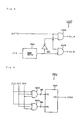
- FIG. 1 is a block diagram illustrative schematically of an entire configuration of a semiconductor memory in accordance with the first embodiment of the present invention.
- FIG. 2 is flow chart illustrative of operations of an operation mode entry circuit in accordance with the first embodiment of the present invention.
- FIG. 3 is a timing chart describing operations of an operation mode entry circuit in accordance with the first embodiment of the present invention.
- FIG. 4 is a view describing a configuration of command data in accordance with the first embodiment of the present invention.
- FIG. 5 is a block diagram illustrative of a configuration of an operation mode entry circuit in accordance with the first embodiment of the present invention.
- FIG. 6 is a block diagram illustrative of a detailed configuration of a main part of an operation mode entry circuit in accordance with the first embodiment of the present invention.
- FIG. 7 is a circuit diagram illustrative of an example of a configuration of a mode judging unit in an operation mode entry circuit in accordance with the first embodiment of the present invention.
- FIG. 8 is a circuit diagram illustrative of an example of a configuration of a latch control unit in a mode judging unit in accordance with the first embodiment of the present invention.
- FIG. 9 is a circuit diagram illustrative of an example of a configuration of a read write judging unit in an operation mode entry circuit in accordance with the first embodiment of the present invention.
- FIG. 10 is a timing chart schematically describing operations of an operation mode entry circuit in accordance with the first embodiment of the present invention.
- FIG. 11 is a timing chart schematically describing operations of a mode judging unit in accordance with the first embodiment of the present invention.
- FIG. 12 is a timing chart schematically describing operations of a read write judging unit in accordance with the first embodiment of the present invention.
- FIG. 13 is a circuit diagram illustrative of an example of a configuration of a mode judging unit in accordance with the second embodiment of the present invention.
- FIG. 14 is a circuit diagram illustrative of an example of a configuration of an operation mode entry circuit in accordance with the third embodiment of the present invention.
- FIG. 15 is a timing chart describing operations of an operation mode entry circuit in accordance with the third embodiment of the present invention.
- FIG. 1 is illustrative schematically of an entire configuration of a semiconductor memory in accordance with the first embodiment of the present invention.
- This semiconductor memory is one kind of non-synchronous pseudo SRAM based on dynamic RAM and is configured to enable an operation mode entry according to command data during operation. Notwithstanding, this invention should not be limited to the pseudo SRAM and may be applicable to any non-synchronous memory devices.
- an address input circuit AIN is to fetch an address ADD from outside.
- a memory cell array MARY comprises a matrix array of dynamic memory cells. In this memory cell array MARY, word lines and bit lines are routed in the form of rows and columns.
- a row decoder XDEC selects a row of the memory cell array MARY based on a row address fetched by the address input circuit AIN.
- a sense amplifier SAMP amplifies data signals appearing on bit lines in the memory cell array MARY.
- a column decoder YDEC selects a column of the memory cell array MARY based on a column address fetched by the address input circuit AIN. Subjected to read is corresponding one of data signals amplified by the sense amplifier SAMP to a column selected by the column decoder YDEC.
- a data input output circuit DIO is to input and output data DQ.
- a refresh control circuit RSH performs sequential controls for designating a memory cell array to be selected for refresh.
- a voltage generating circuit VGEN generates a variety of internal voltages, and has a function of generating a boosted voltage for driving a word line, a function of generating a substrate voltage which provides a bias to a substrate of the memory cell array, and a function of generating a refresh voltage to be referred by the sense amplifier in amplifying data signal.
- An operation mode entry circuit MOD is a feature of the present invention and enters an operation mode designated by command data and mode data MDATA to be used for changing functions of various circuit blocks such as the above-described refresh control circuit in accordance with the contents of the operation mode.
- This operation mode entry circuit MOD stores a final address “1FFFFFh” (h: hexadecimal) and a top address “000000h”.
- This operation mode entry circuit MOD is configured to accept a request for an operation mode entry if read cycles for the final address are continued and to decide an operation mode to be entered based on data designated by a write cycle following to those read cycles.
- a chip select signal /CS is an external control signal for controlling this semiconductor memory in a stand-by state.
- An output enable signal /OE is to control an output impedance state of the data input output circuit DIO.
- a write enable signal /WE is to switch a write operation and a read operation.
- FIG. 2 is a flow chart showing flows of operations for entry of the operation mode
- FIG. 3 is a timing chart of signals related to the operation mode entry.
- the operation mode entry circuit MOD compares an external address ADD to the final address “1FFFFFh” and judges whether or not the externally designated address ADD is the final address in every cycles (step S 1 ).
- the external address ADD is not the final address, and thus the address ADD is not identical with the final address. In this case, this judgement process will be repeated until an external address ADD identical with the final address is designated (step S 1 : NO).
- the final address “1FFFFFh” is designated as the external address ADD, and thus the external address ADD is identical with the final address.
- the operation mode entry circuit MOD judges that the external address ADD is the final address (step S 1 : YES).
- the operation mode entry is enabled (step S 3 ). Namely, the operation mode entry is enabled under conditions that the read cycles are continued for the final address as the specific address, and the request for the operation mode entry is accepted. Assuming that in the read cycle T 4 , the final address is not designated, the process will be back to the above-described step S 1 and the same processes will then be repeated. As described above, the request for the operation mode entry is accepted.
- a top address is designated externally as the external address ADD, and command data for designating the kind of the operation mode to be entered are designated as data DQ.
- the kinds of the operation mode to be entered there are a partial refresh mode, a page length setting mode, and a test mode.
- the kind of the operation mode is designated by two-bits data as data DQ applied to data terminals I/O 1 and I/O 2 in the write cycle T 5 . Since the partial refresh mode is subjected to the entry, then data “0” are externally applied to the data terminals I/O 1 and I/O 2 respectively in accordance with the example shown in FIG. 4 ( a ).
- a detecting signal SCW is to detect the top address in the write cycle
- a detecting signal SCR is to detect the final address in the read cycle and are generated inside of the operation mode entry circuit MOD. This signal will be described in details later.
- the operation mode entry circuit MOD judges whether or not the externally designated address ADD is the top address (step S 4 ). If it is the top address, then the operation mode entry circuit MOD sets a kind of the operation mode based on data DQ designated as the above-described command data (step S 5 ). The operation mode entry circuit MOD outputs mode data MDATA which designate the partial refresh mode as the operation mode to be set. Assuming that the top address is not designated (step S 4 : NO), then the processes will be back to the above-described step S 1 and the above-described sequential steps will be repeated.
- the operation mode entry circuit MOD compares the addresses similarly to the above-described step S 4 .
- the operation mode entry circuit MOD sets a scale of a storage area to be refreshed or a scale of a memory cell array to be refreshed as detailed conditions for the partial refresh mode.
- the operation mode entry circuit MOD will back the process to the above-described step S 1 and repeat the above-described sequential steps. As described above, the operation mode to be entered is decided. Thereafter, the semiconductor memory operates in the partial refresh mode.
- FIG. 4 ( b ) shows a scale of a storage area which is allowed to be designated as detailed conditions for the partial refresh mode. Command data for designating these detailed conditions are designated by two-bits data as data DQ applied to data terminals I/O 1 and I/O 2 in the write cycle T 6 .
- two-bits data applied to the data terminals I/O 1 and I/O 2 are “0, 0”, then a storage area corresponding to 16 megabits is designated. If the two-bits data applied to the data terminals I/O 1 and I/O 2 are “1, 0”, then a storage area corresponding to 8 megabits is designated.
- the a word number which represents the page length is designated as command data (data DQ) for data indicating the conditions of the operation mode as shown in FIG. 4 ( c ).
- the page length is designated by single bit data applied to a data terminal I/O 3 . If data applied to the data terminal I/O 3 is “0”, then the page length is 4-words. If data applied to the data terminal I/O 3 is “1”, then the page length is 8-words.
- FIG. 5 shows a schematic configuration of the operation mode entry circuit MOD.
- a read write judging unit RWJ judges whether the current cycle is the read cycle or the write cycle based on the output enable signal /OE and the write enable signal /WE, and outputs a read write identity signal SRW.
- a mode judging unit ADJ judges whether the request for entry is present or absent based on the address ADD designated in the read cycle., and output a mode entry signal MENT.
- a mode setting unit CDE generates and outputs mode data MDATA based on the data DQ if the request for entry is present, wherein the data DQ are supplied externally as the command data.
- a pulse signal SATD is generated upon detection of a transition of the address ADD by an address transition detecting circuit (ATD) which is not illustrated.
- FIG. 6 shows an example of configurations of the mode judging unit ADJ and the mode setting unit CDE.
- a read address register RREG stores the final address.
- a read address comparator RCMP compares the final address to the external address ADD, and outputs an address detecting signal SCR if the identity between the externally entered address ADD and the final address is detected.
- An address judging circuit MDJ receives the pulse signal SATD and the address detecting signal SCR, and judges whether or not read cycles are continued for the final address.
- a write address register WREG stores the top address.
- a write address comparator WCMP compares the top address to the external address ADD. Those are similar to the above-described read address register RREG and the read address comparator RCMP, except that the top address is detected and the address detecting signal SCW is outputted.
- a command decoder MDS receives the external data DQ and the address detecting signal SCW and generates the mode data MDATA.
- FIG. 7 shows a detailed example of the configuration of the mode judging unit ADJ.
- an address detecting unit ADET detects a specific address ADDR (hereinafter referred to as a specific read address) to be designated externally in a read cycle for the operation mode entry.
- This address detecting unit ADET comprises a read address register RREG and a read address comparator RCMP.
- the read address register RREG stores the final address as the specific read address ADDR.
- the read address comparator RCMP compares the specific read address ADDR stored in the read address register RREG to the address ADD designated sequentially and externally, and outputs an address detecting signal SCR if they are identical with each other.
- Latches LATA and LATB latch the address detecting signal SCR based on latch signals SLA and SLB and output address detecting signals SCA and SCB, respectively.
- a logic-AND gate GA operates a logical-AND of the address detecting signals SCA and SCB, and outputs a result of the operation as the mode entry signal MENT.
- a latch control unit LCNT controls operations of the above-described latches LATA and LATB. The latches LATA and LATB, the logic-AND gate GA, and the latch control unit LCNT perform as the address judging circuit MDJ which receives the address detecting signal SCR and judges that at least two read cycles are continued for the specific read address ADDR.
- FIG. 8 shows an example of the configuration of the latch control unit LCNT.
- a toggle flip-flop (T-FF) TRF inverts the output signal by triggering a negative edge of the chip select signal /CS.
- An inverter GN outputs an inverted signal from the output signal from the toggle flip-flop TRF.
- the logic-AND gate GAA receives the pulse signal SATD and the output signal from the inverter GN, and outputs the latch signal SLA.
- the logic-AND gate GAB receives the pulse signal SATD and the output signal from the toggle flip-flop TRF, and outputs the latch signals SLA and SLB.
- the latch control unit LCNT causes alternating appearances of the pulse signal SATD and the latch signal SLA or SLB by triggering the negative edge of the chip select signal /CS.
- FIG. 9 shows an example of the configuration of the read write judging unit RWJ shown in FIG. 5 .
- logic-AND gates GAC and GAD are provided.
- the logic-AND gate GAC receives inversion inputs of the chip select signal /CS and the output enable signal /OE, and an input of the write enable signal /WE.
- the logic-AND gate GAD receives inversion inputs of the chip select signal /CS and the write enable signal /WE, and an input of the output enable signal /OE.
- a reset-set-flip-flop (RS-FF) RSF receives, at an S-terminal, a set signal SE from the logic-AND gate GAC, and also receives, at an R-terminal, a reset signal RE from the logic-AND gate GAD, and outputs, from a Q-terminal, a read write identity signal SRW.
- This read write judging unit RWJ causes that the read write identity signal SRW to be high level in the read cycle and to be low level in the write cycle.
- FIG. 10 is a timing chart describing operations of the operation mode entry circuit MOD shown in FIG. 5 .
- FIG. 11 is a timing chart describing operations of the mode judging unit ADJ shown in FIGS. 6-8 .
- FIG. 12 is a timing chart describing operations of the read write judging unit RWJ shown in FIG. 9 .
- the operation mode entry circuit MOD shown in FIG. 5 will schematically be described with reference to FIG. 10 .
- the write enable signal /WE is held in the high level, and the chip select signal /CS and the output enable signal /OE are set in the low level in synchronizing with the operation cycle.
- the address ADD is designated in every cycles. If the address ADD is transitioned when the cycle is switched, then the transition of this address ADD is detected by an address transition detecting circuit not illustrated and the pulse signal SATD is generated.
- the read write judging unit RWJ outputs of the high level of the read write identity signal SRW in the read cycles T 1 ⁇ T 4 and then outputs the low level of the read write identity signal SRW in the subsequent write cycles T 5 and T 6 .
- the mode judging unit ADJ judges that the request for the operation mode entry has been made, if the read accesses for the final address are continued in the two cycles in a period of time, wherein the read write identity signal SRW is in the high level.
- the mode judging unit ADJ outputs the high level of the mode entry signal MENT upon receipt of the request. In the example shown in FIG. 10 , the read cycles for the final address “1FFFFFh” are continued in the cycles T 3 and T 4 , and in these cycles, the mode entry signal MENT is in the high level.
- the mode setting unit CDE generates the mode data MDATA based on the external data DQ if the read write identity signal SRW is in the high level in the above-described read cycle T 4 , and in the write cycles T 5 and T 6 following to the read cycle T 4 , the top address “000000h” is designated as the address ADD. In this case, the data input output circuit DIO is inactivated and the output of the read data are inhibited.
- the mode data MDATA are a set of data which are necessary for re-routine of signal paths in an internal circuit of the semiconductor memory in accordance with the operation mode to be entered.
- the mode data MDATA have previously been prepared according to the operation mode.
- a state of the internal circuit of the semiconductor memory is switched for enabling operations in the entered operation mode, namely for deciding the entered operation mode.
- the kind of the operation mode is decided.
- the detailed conditions for the operation mode are decided.
- the kind and the detailed conditions of the operation mode are set according to the above-described example shown in FIG. 4 .
- data DQ which specify the “partial refresh mode” as the kind of the operation mode.
- other data are designated as data DQ, which specify the scale of the storage area to be refreshed, whereby the operation mode to be entered is decided and the mode data MDATA according to this operation mode are generated.
- the semiconductor memory in accordance with the present invention is a non-synchronous memory in view of its performance, and thus does not need any external synchronizing signal for the normal operations such as the data write operation and the data read operation based on the chip select signal /CS and the address ADD.
- the semiconductor memory in accordance with the present invention is to set the operation mode if the same address is designated in the continuous cycles.
- the semiconductor memory is configured to change the chip select signal /CS for every cycles and to use the chip select signal /CS as a synchronizing signal for effectively preventing any erroneous entry.
- the mode judging unit ADJ outputs the mode entry signal MENT if the final address “1FFFFFh” is designated continuously in the two cycles.
- an initial stable state of the toggle flip-flop TRF shown in FIG. 8 is decided.
- the latch signal SLA is in the high level and the latch signal SLB is in the low level.
- the read write judging unit RWJ operates to output the high level of the read write identity signal SRW to be described below.
- the logic-AND gate GA shown in FIG. 7 is activated upon receipt of the read write identity signal SRW, and outputs the mode entry signal MENT in accordance with a combination of the address detecting signals SCA and SCB. Also, the latch control unit LCNT operates to output the latch signals SLA and SLB alternatively for every read cycles.
- the read address comparator RCMP constituting the address detecting unit ADET compares the externally designated address ADD to the final address “1FFFFFh” stored as the specific read address ADDR in the read address register RREG. If an identity between them is detected, the read address comparator RCMP outputs the high level of the address detecting signal SCR.
- the external address ADD is identical with the final address in the read cycles T 3 and T 4 , whereby the high level of the address detecting signal SCR is outputted.
- the address detecting signal SCR is fetched into any one of the latches LATA and LATB based on the latch signals SLA and SLB.
- the latch signal SLA is in the high level, whereby the address detecting signal SCR is fetched into the latch LATA, and then outputted as the address detecting signal SCA.
- the latch LATB has already obtained the low level of the address detecting signal SCR, for which reason in the read cycle T 3 , the latch LATB outputs the low level of the address detecting signal SCB. Therefore, the logic gate GA, which have received the address detecting signals SCA and SCB, will output the low level of the mode entry signal MENT.
- the latch LATB is placed into the high level, whereby the address detecting signal SCR is fetched into the other latch LATB, and then outputted as the address detecting signal SCB.
- the external address ADD remains to be the final address “1FFFFFh”, for which reason the address detecting signal SCR is kept in the high level. Since the latch LATA has obtained the high level in the read cycle T 3 , then in the write cycle T 4 , the address detecting signal SCB is held in the high level. Thus, the logic gate GA outputs the high level of the mode entry signal MENT.
- the high level of the mode entry signal MENT is outputted if the final address “1FFFFFh” is continuously designated in the two cycles. This signal makes it possible to confirm the request for the entry.
- the read write judging unit RWJ identifies the read cycle (the read operation) and the write cycle (the write operation) from the combinations of the chip select signal /CS, the output enable signal /OE, and the write enable signal /WE.
- the logic-AND gate GAC outputs the high level of the set signal SE in those cycles.
- the logic-AND gate GAD keeps the low level of the reset signal RE, for which reason the set-rest flip-flop RSF outputs the high level of the read write identity signal SRW.
- the logic-AND gate GAD outputs the high level of the reset signal RSE in those cycles.
- the logic-AND gate GAC keeps the low level of the set signal SE, for which reason the set-rest flip-flop RSF outputs the low level of the read write identity signal SRW.
- the read write identity signal SRW is kept in the high level if the read cycles are continued, and is kept in the low level if the write cycles are continued. Accordingly, the read cycle and the write cycle can be identified based on the read write identity signal SRW.
- the operation mode entry of the semiconductor memory of the first embodiment has been completed. Thereafter, the semiconductor memory operates in the operation mode as entered.
- the read write judging unit RWJ judges whether the current cycle is the read cycle or the write cycle, and outputs the read write identity signal SRW which identifies the read or write cycle.
- the mode judging unit ADJ judges whether or not the externally entered address ADD is identical with the final address in each cycle and outputs the mode entry signal MENT if the read cycles for the final address are continued.
- the mode setting unit CDE decodes the externally designated data DQ upon input of the mode entry signal MENT and generates the mode data MDATA if the current cycle is the write cycle and the external address is identical with the top address.
- the timing specification of the read cycle and the write cycle are the same as the normal timing specification, for which reason it is unnecessary to prepare any specific or unique timing specification for the system side who uses the semiconductor memory. Accordingly, the operation mode entry can be made without making the timing design complicated.
- the operation mode entry is accepted so as to effectively prevent the erroneous entry.
- the operation mode entry is enabled if the two read accesses to the final address are continued, even the final address has less frequency in use for the normal applications, thereby to minimize the restriction to the address space over the applications.
- a mode judging unit ADJ 2 shown in FIG. 13 is provided instead of the mode judging unit ADJ shown in FIG. 5 .
- the mode judging unit ADJ 2 includes a shift register SREG instead of the latches LATA and LTAB and the latch control circuit LCNT included in the mode judging unit ADJ shown in FIG. 7 .
- This shift register SREG comprises a register RA and a register RB.
- the shift register SREG takes an address detecting signal SC into the register RA on the first stage and shifts the address detecting signal SC into the register RB on the follower stage.
- the contents stored in the shift register SREG are sequentially renewed along the progress of the cycles, whereby the register RA always stores the address detecting signal SCR obtained in the new cycle, and the register RB always stores the address detecting signal SCR obtained in the previous cycle.
- the address detecting signals SCR obtained in the registers RA and RB are outputted as address detecting signals SRA and SRB respectively, which are then inputted into the logic-AND gate GA.
- the logic-AND gate GA receives the address detecting signals SRA and SRB and performs an AND-operation and outputs the mode entry signal MENT.
- the mode entry signal MENT is in the high level if the address detecting signals SRA and SRB outputted from the registers RA and RB are in the high level. This means that the identity of the address ADD with the final address is detected in both the current cycle and the previous cycle. Accordingly, similarly to the above-described first embodiment, if the read cycles for the final address are continued, then the mode entry signal MENT is in the high level. Other operations are similar to the above-described first embodiment.
- the mode judging unit ADJ 2 of the second embodiment does not need the chip select signal /CS and allows simplifying the circuit configuration as compared to the mode judging unit ADJ 1 of the above-described first embodiment.
- the two-stage shift register is used.
- the number of the stages may be optional.
- a three-stage shift register may be utilized to accept the entry if the three read cycles for the final address are continued.
- the read address comparator RCMP compares the external address ADD with the final address stored in the read address register RREG and judges whether or not the final address is designated (step S 1 ). In read cycles T 1 and T 2 , the external address ADD is not the final address, and thus the address ADD is not identical with the final address. In this case, this judgement process will be repeated until the identity between them can be detected (step S 1 : NO).
- the final address “1FFFFFh” is designated as the external address ADD, and thus the external address ADD is identical with the final address.
- the read address comparator RCMP judges that the external address ADD is the final address, and outputs the high level of the address detecting signal SCR (step S 1 : YES).
- the address detecting signal SCR is kept in the high level (step S 2 : YES). If in the read cycle T 4 , the final address is not designated, then the process will be back to the above-described step S 1 and the same processes will then be repeated. As described above, the request for the operation mode entry is accepted.
- the write address comparator WCMP compares the external address ADD to the top address “000000h” stored in the write address register WREG, and judges whether or not the top address is designated (step S 4 ). If the top address is designated, then the command decoder MDS sets a kind of the operation mode (step S 5 ). The command decoder MDS outputs mode data MDATA which designate the partial refresh mode as data representing the kind of the operation mode to be set. If the top address is not designated (step S 4 : NO), then the processes will be back to the above-described step S 1 and the above-described-sequential steps will be repeated.
- the write address comparator WCMP compares the addresses similarly to the above-described step S 4 .
- the read write identity signal SCW is outputted.
- the command decoder MDS sets the detailed conditions for the operation mode. In this example, the storage area is set, which is to be refreshed in the partial refresh mode. If the top address is not designated in the write cycle T 6 (step S 6 : NO), then the process will be back to the above-described step S 1 and the above-described sequential steps will be repeated. As described above, the operation mode to be entered is decided. Thereafter, the semiconductor memory operates in the partial refresh mode.
- the sequential judgement processes are executed on the software with reducing the load to the hardware. Notwithstanding, it is possible that the sequential processes functions are realized on the hardware.
- the predefined timing specification may be applicable to the timing specification for the read cycle and the write cycle even for the entry of the operation mode. Accordingly, the high speed entry of the operation mode can be made with the operations in the minimum cycle time.
- FIG. 14 is a view showing the configuration of the third embodiment of the present invention.
- FIG. 14 shows one example of the configuration of the operation mode entry circuit MOD shown in FIG. 1 .
- the mode data MDATA in FIG. 1 are the partial refresh switching signal.
- This third embodiment is to prevent the erroneous entry of the mode to the address skew.
- the operation mode entry circuit in accordance with this embodiment includes an address register AREG for storing a programmed address, an address comparator ACMP for receiving an address signal ADD and an address in the address register AREG and compares the input two addresses, an inverter INV 1 for receiving a chip select signal /CS through a control terminal and for outputting an inverted signal thereof, a one-shot pulse generator PG 1 for receiving the output signal (the inversion signal of the chip select signal /CS) and generating one-shot pulse signal with a predetermined pulse width which synchronizes with a transition into the low level of the chip select signal /CS, an inverter INV 2 for receiving the output enable signal /OE through a control terminal and for outputting an inverted signal thereof, an inverter INV 3 for receiving the write enable signal /WE through a control terminal and for outputting an inverted signal thereof, a register REG 3 for sampling and outputting the output signal from the address comparator ACMP at a rising
- the operation mode entry circuit in accordance with this embodiment further includes a register REG 1 for sampling and outputting the output signal from the address comparator ACMP at a rising edge of the signal PRE outputted from the logic-AND gate circuit AND 1 , a register REG 2 for sampling and outputting the output signal from the register REG 1 at a rising edge of the signal PRE, a logic-NAND gate circuit NAND 1 for receiving the output signal from the register REG 1 and the output signal from the register REG 1 through two input terminals and for outputting a logic-NAND of the two input signals, and an SR-flip-flop (also so called to as RS-flip-flop) for receiving the output signal from the logic-NAND gate circuit NAND 1 as a set signal SET and the output signal from the register REG 3 as a reset signal RES.
- a register REG 1 for sampling and outputting the output signal from the address comparator ACMP at a rising edge of the signal PRE outputted from the logic-AND gate circuit AND 1
- a register REG 2
- This non-synchronous SR-flip-flop comprises two logic-NAND gate circuits NAND 2 and NAND 3 .
- the logic-NAND gate circuit NAND 2 receives the output signal SET from the logic-NAND gate circuit NAND 1 and the output signal from the logic-NAND gate circuit NAND 3 , and outputs the mode entry signal MENT from its output terminal.
- the logic-NAND gate circuit NAND 3 receives the output signal RES from the register REG 3 and the output signal from the logic-NAND gate circuit NAND 2 . If the signal SET is in the high level and the signal RES is also in the high level, then this SR-flip-flop holds the present state.
- the mode entry signal MENT If the mode entry signal MENT is in the low level, and the signal SET becomes the low level and the signal RES remains in the high level, then the mode entry signal MENT becomes the high level (the mode entry signal MENT is set). If the mode entry signal MENT is in the high level, and the signal SET is in the high level and the signal RES is in the low level, then the mode entry signal MENT becomes the low level (the mode entry signal MENT is reset). If the SR-flip-flop comprises the two logic-NAND gate circuits NAND 2 and NAND 3 as shown in FIG. 14 , then the SR-flip-flop is activated if both the signals SET and RESET are in the low level. This SR-flip-flop may comprise two logic-NOR gate circuits NOR.
- NAND 1 in FIG. 14 may be replaced by the logic-AND gate circuits, and the output signal from the register REG 3 is inverted by the inverter and the inverted signal is inputted into the reset terminal of the SR-flip-flop.
- the operation mode entry circuit in accordance with the present invention further includes a register REG 6 for sampling and outputting the data (Data) inputted through the DQ terminal (refer FIG. 1 ) in the write cycle with an output signal WRE 1 from the logic-AND gate circuit AND 2 , a mode selecting circuit MODSEL for decoding the output signal from the register REG 6 and selecting the mode, a two-input logic-AND gate circuit AND 3 for receiving the output signal from the mode selecting circuit MODSEL and the output signal from the one-shot pulse generator PG 1 , and a register REG 7 for sampling and outputting the data (Data) inputted through the DQ terminal in the write cycle with an output signal WRE 2 from the logic-AND gate circuit AND 3 .
- An address register AREG and an address comparator ACMP in FIG. 14 correspond to the address judging unit in the above-described second embodiment.
- Registers REG 1 and REG 2 correspond to the two-staged registers RA and RB shown in FIG. 13 .
- the registers REG 1 and REG 2 are different in those timing control signals from the registers RA and RB shown in FIG. 13 .
- This embodiment is different from the above-described second embodiment in view that the single address register is provided instead of the read address register and the write address register, and also the specific address is common to both the read cycle and the write cycle.
- the SR-flip-flop I provided instead of the gate GA shown in FIG. 13 .
- a sampling control signal (“latch timing signal” or “sampling clock signal”) for the registers REG 1 and REG 2 and a reset signal of the SR-flip-flop are generated based on the output signal from the address comparator ACMP, the chip select signal /CS and the output enable signal /OE.
- the sampling control signal PRE for the registers REG 1 and REG 2 is in the high level, if the chip select signal /CS becomes the low level (the output signal from the one-shot pulse generator PG 1 is transitioned to the high level), and the address comparator ACMP detects the address identity (the output signal from the address comparator ACMP is in the high level), and the output enable signal /OE is in the low level.
- the output signals from the registers REG 1 and REG 2 are transitioned to the high level at the rising edge of the signal PRE, whereby the set signal SET is transitioned into the low level, and the mode entry signal MENT as the output signal from the SR-flip-flop is set in the high level.
- the output signal RES from the register REG 3 is transitioned into the low level in synchronizing with the transition into the low level of the chip select signal /CS if the address comparator ACMP detects the non-identity of the address (outputs the low level), whereby the output signal (the mode entry signal MENT) from the SR-flip-flop is reset in the low level.
- the logic-AND gate circuits AND 2 and AND 3 , the mode selecting circuit MODSEL, the registers REG 6 and REG 7 , and the partial refresh switching circuit PEGEN constitute the mode setting unit which receives the kind of the mode and the condition for the mode set in the write cycle upon the active state of the mode entry signal MENT and performs the mode entry.
- FIG. 15 is a view showing one example of the operation of generating the mode entry signal MENT and the timing operation of setting the mode if the mode entry signal MENT is in the active state under the configuration shown in FIG. 14 .
- FIG. 15 schematically shows timing waveforms of the address signal ADD, and the chip select signal /CS, the output enable signal /OE and the write enable signal /WE supplied to the control terminals of the semiconductor memory, as well as signals PRE, SET, RES, MENT and WRE 1 generated inside of the operation mode entry circuit.
- the chip select signal /CS is set in the active state as the initial state for the memory cycle similarly to the above-described first and second embodiments (it is transitioned into the low level in this embodiment).
- the output enable signal /OE is set in the low level for the read access and in the high level for the write access in a predetermined initial time period for the memory cycle.
- the write enable signal /WE is activated in the low level for the write access in a predetermined initial time period for the memory cycle.
- the output enable signal /OE is transitioned from the low level to the high level in a period of time of the data output for the read cycle (refer cycles T 1 and T 2 in FIG.
- the data input output circuit DIO disables data output from an output buffer (not shown).
- Data having read out of the memory cell array in the read cycle for the mode entry are not supplied to a data bus (not shown) from the data terminal DQ (namely, this means dummy cycle).
- the output enable signal /OE is held in the low level, and the data are supplied from the data terminal DQ and then the read data are considered to be null by a processor.
- the address signal ADD is not “1FFFFFh”, for which reason any operation for the operation mode entry is not made (the normal operation is made).
- the address ADD is “1FFFFFh”, and thus the output signal RES from the register REG 3 , which latches the output signal from the address comparator ACMP, is transitioned to the high level, at a rising edge of a pulse signal (not shown) outputted from the one-shot pulse generator PG 1 when the chip select signal /CS is transitioned into the low level.
- the address signal ADD is “1FFFFFh”, and the output from the address comparator ACMP is in the high level. If the chip select signal /CS is transitioned into the low level (the output signal from the one-shot pulse generator PG 1 is transitioned into the high level) and the address comparator ACMP detects the address identity and the output enable signal /OE is in the low level, then the signal PRE is transitioned to the high level and then supplied as the sampling control signal to the registers REG 1 and REG 2 .
- the output signal RES from the register REG 3 which latches the output signal from the address comparator ACMP at the rising edge of the one-shot pulse upon the transition into the low level of the chip select signal /CS, remains in the high level. Since both the output signals from the registers REG 1 and REG 2 are in the high level, the output signal from the logic-NAND gate circuit NAND 1 is in the low level, while the mode entry signal MENT is in the high level.
- the address signal ADD is “1FFFFFh”, and the output from the address comparator ACMP is in the high level. If the chip select signal /CS is transitioned into the low level (the output signal from the one-shot pulse generator PG 1 is transitioned into the high level) and the output from the address comparator ACMP is in the high level and the output enable signal /OE is in the high level, then the signal PRE as the output signal from the logic-AND gate circuit AND 1 is transitioned to the low level and not risen, whereby the registers REG 1 and REG 2 hold the previous states. Further, the output signal RES from the register REG 3 remains in the high level.
- the output signal SET from the logic-NAND gate circuit NAND 1 is in the low level, while the mode entry signal MENT is in the high level.
- the data indicating the kind are inputted to the data terminal, and the entered data are fetched into the register at the rising edge of the signal WRE 1 .
- the mode selecting circuit MODSEL receives and decodes the output signal from the register REG 6 , and activates the output signal (high level) if the output signal from the register REG 6 is a predetermined mode.
- the mode selecting circuit MODSEL identifies that the operation mode is the partial refresh mode (FIG. 4 ( b )), then the mode selecting circuit MODSEL places the output signal into the active state.
- the address signal ADD is “1FFFFFh”, and the output from the address comparator ACMP is in the high level.
- the chip select signal /CS is transitioned into the low level (the output signal from the one-shot pulse generator PG 1 is transitioned into the high level) and the output from the address comparator ACMP is in the high level and the output enable signal /OE is in the high level
- the signal PRE as the output signal from the logic-AND gate circuit AND 1 is transitioned to the low level and not risen, whereby the registers REG 1 and REG 2 hold the previous states.
- the output signal RES from the register REG 3 remains in the high level.
- the output signal SET from the logic-NAND gate circuit NAND 1 is in the low level, while the mode entry signal MENT is in the high level.
- the data indicating conditions are inputted into the data terminal DQ, and the entered condition data are sampled by the register REG 7 at a riding edge of a signal WRE 2 .
- the signal WRE 2 is the one shot pulse signal which was generated by the one-shot pulse generator PG 1 at a falling edge of the chip select signal /CS and then passed through the logic-AND gate circuit AND 3 which receives the activated signal outputted from the mode selecting circuit MODSEL.
- the condition data fetched into the register REG 7 in the cycle T 4 are then supplied to the partial refresh switching circuit PEGEN.
- the partial refresh switching circuit PEGEN outputs partial refresh switching signals PEn, PEn- 1 and PEn- 2 . Values set for the partial refresh switching signals PEn, PEn- 1 and PEn- 2 are held until the next partial refresh switching signals are set in the power-on state.
- the address signal ADD is not “1FFFFFh”, whereby the output from the address comparator ACMP is in the low level.
- the output signal RES from the register REG 3 is transitioned to the low level at the rising edge of the one-shot pulse generated by the one-shot pulse generator PG 1 at the falling edge of the chip select signal /CS, whereby the mode entry signal MENT as the output signal from the SR-flip-flop is transitioned into the low level.
- the sampling control signal WRE 1 is in the low level, whereby the data are not sampled by the register REG 6 .
- the output signal from the mode selecting circuit MODSEL is not activated, and the sampling control signal WRE 2 is in the low level, whereby the data are not sampled by the register REG 7 .
- data for the kind and condition may be set in width of data, so that they are fetched in one write cycle, or the data for the kind and condition may be set in at least two write cycles.
- Set values for the partial refresh switching signals PEn, PEn- 1 and PEn- 2 are supplied as the mode data MDATA to the refresh control circuit RSH shown in FIG. 1 , wherein the values of the partial refresh switching signals PEn, PEn- 1 and PEn- 2 are supplied to a refresh address generating circuit (not shown) in the refresh control circuit RSH, so that respective logic operations (for example, NOR-operation) between the values of the partial refresh switching signals PEn, PEn- 1 and PEn- 2 and the most significant bit, the second significant bit and the third significant bit of the refresh address are made and results of the operations are supplied to a row decoder for the refresh operation.
- logic operations for example, NOR-operation
- the partial refresh switching signal PEn is in the high level, then the most significant bit of the refresh address is set in the low level (is masked), and a half of the memory area is refreshed. If the partial refresh switching signals PEn and PEn- 1 are in the high level, then the most significant bit and the second significant bit of the refresh address are set in the low level (are masked), and one quarter of the memory area is refreshed.
- the partial refresh switching signals PEn, PEn- 1 and PEn- 2 may be supplied as the mode data MDATA to the voltage generating circuit VGEN (refer FIG. 1 ), so that the voltage generating circuit VGEN performs a power supply for the partial refresh operation in the stand-by state based on those signals.
- a skew generated on the address signal in the system is inputted into the address terminal of the memory chip, and the designation of the same address by the processor cases the address skew.
- the chip select signal /CS which is transitioned to the active state in every access cycles, is used to generate the timing edge as the trigger for fetching the address for every cycles and the prevention to the erroneous entry due to the address skew can be realized.
- the operation mode entry circuit MOD is not essential that the operation mode entry circuit MOD is provided in the same chip as the semiconductor memory. It is also possible that the operation mode entry circuit MOD is connected to a processor and a part or all of the functions of the operation mode entry circuit MOD is provided in a memory controller IC which controls the semiconductor memory. Needless to say, the present invention may be applicable to a configuration that a variety of logic circuits such as the memory, the processor and the memory controller is integrated on the same chip.
- the mode setting unit CDE (refer FIG. 6 ) in the above-described first embodiment is not limited to the above-described configuration that if the write address comparator WCMP detects the address identity, then the command data are entered through the data terminal DQ.
- the command decoder MDS of the mode setting unit CDE may be configured to enter any combination of the signals inputted through the address terminal ADD and/or the predetermined control terminals such as a byte control terminal as the operation mode to be entered (the kind and the condition of the operation mode) if the mode entry signal MENT is in the active state. It is also possible that instead of the data inputted through the data terminal DQ (refer FIG.
- any combination of the signals inputted through the address terminal ADD and/or the predetermined control terminals such as a byte control terminal is inputted as the mode data to be supplied to the register REG 6 and the register REG 7 .
- the operation mode information entered through the data terminal DQ is not to be stored in the memory cell array MARY, but the operation mode information may be signals entered through the address terminal and/or the control terminals for the operation mode entry.
- the operation mode entry circuit MOD is configured to judge whether the current cycle is the read cycle or the write cycle based on the control signal inputted through the control terminal, and if the address is identical with the predetermined read address in the continuous two read cycles, then the operation mode entry circuit MOD places the mode entry signal MENT into the active state. If the condition for enabling the mode entry is the continuation of the read operations for the predetermined address, then this secures the prevention of writing data in the memory cell array (preventing the overwrite). Notwithstanding, the condition for placing the mode entry signal MENT into the active state is not limited to the continuation of the read operations for the predetermined address.
- the mode entry signal MENT is placed into the active state.
- the output signal from the read address comparator RCMP which compares the address stored in the read address register RREG to the input address, is inputted into the latch LATA in FIG. 7 or the register RA in FIG. 13 , as well as the output signal from the write address comparator WCMP (refer FIG.
- the mode entry signal MENT is placed into the active state.
- the output signal from the read address comparator RCMP which compares the address stored in the read address register RREG to the input address, is inputted into the latch LATB in FIG. 7 or the register RB in FIG. 13 , as well as the output signal from the write address comparator WCMP (refer FIG. 6 ), which compares the address stored in the write address register WREG (refer FIG.
- the 14 may be generated by an logical-AND operation by the logic-AND gate of a signal obtained by causing the register REG 3 to sample the output signal from the address comparator ACMP at the rising edge of the one-shot pulse outputted from the one-shot pulse generator PG 1 , another signal obtained by causing the register REG 4 to sample the output enable signal /OE (or the register REG 5 to sample the inversion signal of the write enable signal /WE) at the rising edge of the one-shot pulse outputted from the one-shot pulse generator PG 1 , and the output signal from the one-shot pulse generator PG 1 .
- the mode setting unit CDE is configured to decide the operation mode to be entered based on a signal inputted through at least one of the address terminal, the control terminals and the data terminal, or combinations thereof (for example, a combination of a predetermined bit of the address terminal and a predetermined terminal in the control terminals).
- the present invention provides the follows effects.
- the request for he entry is accepted to decide the operation mode to be entered based on the data designated by the write cycle following to the read cycles, so as to enable the operation mode entry of the semiconductor memory during operation without need of any specific timing specification but with an effective suppression to the erroneous entry.
- the specific address to be designated externally is stored, and the stored specific address is compared to the address designated sequentially and externally, so as to judge that at least two read cycles are continued for the specific address upon result of the comparison result, thereby accepting the request for the entry if the read cycles for the plural addresses are continued.
- the specific address to be designated externally is stored, and the stored specific address is compared to the address designated sequentially and externally, so as to decide the operation mode based ion the data designated in the write cycle upon receipt of the comparison result, whereby the operation mode to be entered is decided based on the data designated in the write cycle following to the read cycles.
- the request for the operation mode entry is accepted to effectively present any erroneous entry.
- the request for the operation mode entry is accepted for avoiding any substantive restriction to the address space in the system side, in which the semiconductor memory is integrated.
- the request for the operation mode entry is accepted with further effective suppression to the erroneous entry.
- a partial refresh mode is accepted for refreshing a partial area of the memory cell array comprising the matrix array of the dynamic memory cells, so as to allow a selective refresh to the storage area based on the scale of the data to be stored, and effectively prevent any unnecessary current consumption for the refresh operation.
- the present invention should not be limited to those embodiments but include any design changes in the extent of the subject matter of the present invention.
- the final address is continuously designated for the plural addresses in the read cycle. Notwithstanding, it is also possible that different addresses from each other are designated for the plural addresses For the write address, different addresses from each other may be designated.
- the top address is designated in the write cycle, while the final address is designated in the read cycle. Notwithstanding, it is also possible that the same address is designated for the read and write cycles.
- the entry is accepted if at least two read cycles are continued. Notwithstanding, it is also possible that the entry is accepted if plural read cycles are continued, wherein increasing the number of the plural read cycles to be continued increase the effect of preventing the erroneous entry.
- the command data are designated in the separate two write cycles for deciding the entry. Notwithstanding, it is also possible that the command data are designated in the single write cycle. It is also possible that the command data are designated in at least three write cycles.
- the chip select signal /CS is transitioned in synchronizing with the address ADD. Notwithstanding, it is also possible that the chip select signal /CS is fixed at the low level (in the active state). In accordance with the above-described embodiments, if the chip select signal /CS synchronizes with the address signal, then the strict condition for accepting the entry is present, which increases the effect of preventing the erroneous entry.
- the descriptions have been made by taking an example that the partial refresh mode is the operation mode to be entered. Notwithstanding, it is also possible that any operation modes for allowing the read operation and the write operation may be subject to the operation mode entry.
- the read address and the write address to be used for the mode entry are the common predetermined address to simplify the configuration.
- a flip-flip is provided which set a signal controlling the enabling of the mode entry in the active state if the access address is identical with the predetermined address, for simplifying the timing design with increasing a stability (time margin) such as an address skew to secure the prevention of the erroneous entry.
- a combination of the read accesses and the write accesses in the predetermined sequence is detected for the predetermined address to place the signal controlling the enabling of the mode entry into the active state, whereby the same effects or at least one of the effects mentioned above can be provided.
Landscapes
- Engineering & Computer Science (AREA)
- Microelectronics & Electronic Packaging (AREA)
- Computer Hardware Design (AREA)
- Dram (AREA)
- Static Random-Access Memory (AREA)
Priority Applications (1)
| Application Number | Priority Date | Filing Date | Title |
|---|---|---|---|
| US11/133,974 US7145812B2 (en) | 2001-02-01 | 2005-05-20 | Semiconductor memory device and method of entry of operation modes thereof |
Applications Claiming Priority (5)
| Application Number | Priority Date | Filing Date | Title |
|---|---|---|---|
| JP2001026148 | 2001-02-01 | ||
| JP2001-26148 | 2001-02-01 | ||
| JP2002-16941 | 2002-01-25 | ||
| JP2002016951A JP3737437B2 (ja) | 2001-02-01 | 2002-01-25 | 半導体メモリ及びその動作モードのエントリー方法 |
| PCT/JP2002/000728 WO2002061754A1 (fr) | 2001-02-01 | 2002-01-30 | Memoire a semi-conducteur et procede d'introduction de mode de fonctionnement |
Related Child Applications (1)
| Application Number | Title | Priority Date | Filing Date |
|---|---|---|---|
| US11/133,974 Division US7145812B2 (en) | 2001-02-01 | 2005-05-20 | Semiconductor memory device and method of entry of operation modes thereof |
Publications (2)
| Publication Number | Publication Date |
|---|---|
| US20040080993A1 US20040080993A1 (en) | 2004-04-29 |
| US6925016B2 true US6925016B2 (en) | 2005-08-02 |
Family
ID=26608810
Family Applications (2)
| Application Number | Title | Priority Date | Filing Date |
|---|---|---|---|
| US10/467,031 Expired - Fee Related US6925016B2 (en) | 2001-02-01 | 2002-01-30 | Semiconductor memory and method for entering its operation mode |
| US11/133,974 Expired - Fee Related US7145812B2 (en) | 2001-02-01 | 2005-05-20 | Semiconductor memory device and method of entry of operation modes thereof |
Family Applications After (1)
| Application Number | Title | Priority Date | Filing Date |
|---|---|---|---|
| US11/133,974 Expired - Fee Related US7145812B2 (en) | 2001-02-01 | 2005-05-20 | Semiconductor memory device and method of entry of operation modes thereof |
Country Status (7)
| Country | Link |
|---|---|
| US (2) | US6925016B2 (fr) |
| EP (1) | EP1367593A4 (fr) |
| JP (1) | JP3737437B2 (fr) |
| KR (1) | KR20030078900A (fr) |
| CN (1) | CN1329921C (fr) |
| TW (1) | TW548651B (fr) |
| WO (1) | WO2002061754A1 (fr) |
Cited By (6)
| Publication number | Priority date | Publication date | Assignee | Title |
|---|---|---|---|---|
| US20040184323A1 (en) * | 2003-03-17 | 2004-09-23 | Fujitsu Limited | Semiconductor memory device with shift register-based refresh address generation circuit |
| US20090245012A1 (en) * | 2008-03-31 | 2009-10-01 | Fujitsu Microelectronics Limited | Semiconductor storage device and memory system |
| US20110058441A1 (en) * | 2009-09-04 | 2011-03-10 | Hynix Semiconductor Inc. | Data line driving circuit |
| US8588017B2 (en) | 2010-10-20 | 2013-11-19 | Samsung Electronics Co., Ltd. | Memory circuits, systems, and modules for performing DRAM refresh operations and methods of operating the same |
| US9531352B1 (en) * | 2015-06-24 | 2016-12-27 | Intel Corporation | Latched comparator circuit |
| US10311936B2 (en) | 2015-08-12 | 2019-06-04 | Samsung Electronics Co., Ltd. | Semiconductor memory device managing flexible refresh skip area |
Families Citing this family (11)
| Publication number | Priority date | Publication date | Assignee | Title |
|---|---|---|---|---|
| JP4707255B2 (ja) * | 2001-04-26 | 2011-06-22 | ルネサスエレクトロニクス株式会社 | 半導体記憶装置 |
| US7793037B2 (en) * | 2005-05-31 | 2010-09-07 | Intel Corporation | Partial page scheme for memory technologies |
| JP4778321B2 (ja) * | 2006-01-30 | 2011-09-21 | 富士通セミコンダクター株式会社 | 半導体メモリ、メモリシステム |
| JP2007200504A (ja) * | 2006-01-30 | 2007-08-09 | Fujitsu Ltd | 半導体メモリ、メモリコントローラ及び半導体メモリの制御方法 |
| JP5096131B2 (ja) * | 2007-12-27 | 2012-12-12 | ルネサスエレクトロニクス株式会社 | 半導体記憶装置 |
| JP5229059B2 (ja) * | 2009-03-31 | 2013-07-03 | 富士通株式会社 | 半導体記憶装置及びその制御方法 |
| US8004870B2 (en) * | 2009-12-24 | 2011-08-23 | Winbond Electronics Corp. | Memory chips and judgment circuits thereof |
| JP5514095B2 (ja) * | 2010-12-24 | 2014-06-04 | ルネサスエレクトロニクス株式会社 | 半導体記憶装置 |
| KR20120074897A (ko) * | 2010-12-28 | 2012-07-06 | 에스케이하이닉스 주식회사 | 모드레지스터세트를 구비하는 반도체 메모리 장치 |
| JP2016208231A (ja) * | 2015-04-21 | 2016-12-08 | 日本電気株式会社 | 論理回路、及び設定回路の制御方法 |
| CN116917991A (zh) * | 2021-05-20 | 2023-10-20 | 华为技术有限公司 | 存储器芯片及其控制方法 |
Citations (5)
| Publication number | Priority date | Publication date | Assignee | Title |
|---|---|---|---|---|
| JPS62180398A (ja) | 1986-02-04 | 1987-08-07 | 日本電気株式会社 | 極パラメ−タ値抽出装置 |
| US5506726A (en) | 1993-08-02 | 1996-04-09 | Tahira; Tadao | Binoculars and camera with binoculars |
| US5521873A (en) | 1993-03-10 | 1996-05-28 | Kabushiki Kaisha Toshiba | Semiconductor dynamic random access memory |
| US5778440A (en) | 1994-10-26 | 1998-07-07 | Macronix International Co., Ltd. | Floating gate memory device and method for terminating a program load cycle upon detecting a predetermined address/data pattern |
| US6246614B1 (en) * | 1999-06-22 | 2001-06-12 | Mitsubishiki Denki Kabushiki Kaisha | Clock synchronous semiconductor memory device having a reduced access time |
Family Cites Families (7)
| Publication number | Priority date | Publication date | Assignee | Title |
|---|---|---|---|---|
| KR960003526B1 (ko) * | 1992-10-02 | 1996-03-14 | 삼성전자주식회사 | 반도체 메모리장치 |
| JPS62180398U (fr) * | 1986-04-30 | 1987-11-16 | ||
| JP3313728B2 (ja) * | 1995-05-26 | 2002-08-12 | マクロニクス インターナショナル カンパニー リミテッド | プログラムロードサイクルを終了させるためのプロトコルを有する浮遊ゲートメモリデバイス |
| JP4000206B2 (ja) * | 1996-08-29 | 2007-10-31 | 富士通株式会社 | 半導体記憶装置 |
| US5956748A (en) * | 1997-01-30 | 1999-09-21 | Xilinx, Inc. | Asynchronous, dual-port, RAM-based FIFO with bi-directional address synchronization |
| KR100306966B1 (ko) * | 1998-08-04 | 2001-11-30 | 윤종용 | 동기형버스트반도체메모리장치 |
| JP3883087B2 (ja) | 1998-11-09 | 2007-02-21 | 富士通株式会社 | 半導体記憶装置及び半導体メモリ回路 |
-
2002
- 2002-01-25 JP JP2002016951A patent/JP3737437B2/ja not_active Expired - Fee Related
- 2002-01-30 US US10/467,031 patent/US6925016B2/en not_active Expired - Fee Related
- 2002-01-30 WO PCT/JP2002/000728 patent/WO2002061754A1/fr not_active Application Discontinuation
- 2002-01-30 CN CNB028044983A patent/CN1329921C/zh not_active Expired - Fee Related
- 2002-01-30 EP EP02710406A patent/EP1367593A4/fr not_active Withdrawn
- 2002-01-30 KR KR10-2003-7010132A patent/KR20030078900A/ko not_active Application Discontinuation
- 2002-02-01 TW TW091101860A patent/TW548651B/zh not_active IP Right Cessation
-
2005
- 2005-05-20 US US11/133,974 patent/US7145812B2/en not_active Expired - Fee Related
Patent Citations (5)
| Publication number | Priority date | Publication date | Assignee | Title |
|---|---|---|---|---|
| JPS62180398A (ja) | 1986-02-04 | 1987-08-07 | 日本電気株式会社 | 極パラメ−タ値抽出装置 |
| US5521873A (en) | 1993-03-10 | 1996-05-28 | Kabushiki Kaisha Toshiba | Semiconductor dynamic random access memory |
| US5506726A (en) | 1993-08-02 | 1996-04-09 | Tahira; Tadao | Binoculars and camera with binoculars |
| US5778440A (en) | 1994-10-26 | 1998-07-07 | Macronix International Co., Ltd. | Floating gate memory device and method for terminating a program load cycle upon detecting a predetermined address/data pattern |
| US6246614B1 (en) * | 1999-06-22 | 2001-06-12 | Mitsubishiki Denki Kabushiki Kaisha | Clock synchronous semiconductor memory device having a reduced access time |
Cited By (14)
| Publication number | Priority date | Publication date | Assignee | Title |
|---|---|---|---|---|
| US20040184323A1 (en) * | 2003-03-17 | 2004-09-23 | Fujitsu Limited | Semiconductor memory device with shift register-based refresh address generation circuit |
| US20060256638A1 (en) * | 2003-03-17 | 2006-11-16 | Fujitsu Limited | Semiconductor memory device with shift register-based refresh address generation circuit |
| US7145825B2 (en) * | 2003-03-17 | 2006-12-05 | Fujitsu Limited | Semiconductor memory device with shift register-based refresh address generation circuit |
| US7286434B2 (en) | 2003-03-17 | 2007-10-23 | Fujitsu Limited | Semiconductor memory device with shift register-based refresh address generation circuit |
| US8139438B2 (en) | 2008-03-31 | 2012-03-20 | Fujitsu Semiconductor Limited | Semiconductor storage device and memory system |
| US20090245012A1 (en) * | 2008-03-31 | 2009-10-01 | Fujitsu Microelectronics Limited | Semiconductor storage device and memory system |
| US8724425B2 (en) | 2008-03-31 | 2014-05-13 | Fujitsu Semiconductor Limited | Semiconductor storage device and memory system |
| US20110058441A1 (en) * | 2009-09-04 | 2011-03-10 | Hynix Semiconductor Inc. | Data line driving circuit |
| US8588017B2 (en) | 2010-10-20 | 2013-11-19 | Samsung Electronics Co., Ltd. | Memory circuits, systems, and modules for performing DRAM refresh operations and methods of operating the same |
| US9531352B1 (en) * | 2015-06-24 | 2016-12-27 | Intel Corporation | Latched comparator circuit |
| US10033360B2 (en) | 2015-06-24 | 2018-07-24 | Intel Corporation | Latched comparator circuit |
| US10311936B2 (en) | 2015-08-12 | 2019-06-04 | Samsung Electronics Co., Ltd. | Semiconductor memory device managing flexible refresh skip area |
| US11631449B2 (en) | 2015-08-12 | 2023-04-18 | Samsung Electronics Co., Ltd. | Semiconductor memory device managing flexible refresh skip area |
| US11887650B2 (en) | 2015-08-12 | 2024-01-30 | Samsung Electronics Co., Ltd. | Semiconductor memory device managing flexible refresh skip area |
Also Published As
| Publication number | Publication date |
|---|---|
| CN1329921C (zh) | 2007-08-01 |
| EP1367593A4 (fr) | 2007-07-11 |
| US20040080993A1 (en) | 2004-04-29 |
| US20050216676A1 (en) | 2005-09-29 |
| EP1367593A1 (fr) | 2003-12-03 |
| TW548651B (en) | 2003-08-21 |
| CN1491418A (zh) | 2004-04-21 |
| KR20030078900A (ko) | 2003-10-08 |
| WO2002061754A1 (fr) | 2002-08-08 |
| JP3737437B2 (ja) | 2006-01-18 |
| JP2002304883A (ja) | 2002-10-18 |
| US7145812B2 (en) | 2006-12-05 |
Similar Documents
| Publication | Publication Date | Title |
|---|---|---|
| US7145812B2 (en) | Semiconductor memory device and method of entry of operation modes thereof | |
| US6463002B2 (en) | Refresh-type memory with zero write recovery time and no maximum cycle time | |
| US7573738B2 (en) | Mode selection in a flash memory device | |
| KR101037637B1 (ko) | 선택적 프리차지를 하는 메모리 | |
| US7242631B2 (en) | Semiconductor memory device and information processing system | |
| US5251176A (en) | Dynamic type semiconductor memory device with a refresh function and method for refreshing the same | |
| US6996016B2 (en) | Echo clock on memory system having wait information | |
| WO2003056563A1 (fr) | Dispositif de stockage a semi-conducteur et son procede de commande de regeneration | |
| US20030226064A1 (en) | Semiconductor memory device | |
| US6466492B2 (en) | Synchronous semiconductor memory device and method for controlling mask data input circuit | |
| US7724593B2 (en) | Memories with front end precharge | |
| US20020136079A1 (en) | Semiconductor memory device and information processing system | |
| KR101088548B1 (ko) | 전단 프리차지를 하는 메모리 | |
| US6961830B2 (en) | Semiconductor memory device with fast masking process in burst write mode | |
| US7764548B2 (en) | Semiconductor memory device which delays refreshment signal for performing self-refreshment | |
| US6903990B2 (en) | Refresh control for semiconductor memory device | |
| US7522458B2 (en) | Memory and method of controlling access to memory | |
| US6917563B2 (en) | Integrated memory | |
| KR20050069453A (ko) | 동적 반도체 메모리 장치 및 이 장치의 절전 모드 동작방법 | |
| US7692988B2 (en) | Semiconductor device and method of controlling the same | |
| US6721224B2 (en) | Memory refresh methods and circuits | |
| KR100275722B1 (ko) | 동기식 랜덤 엑세스 메모리 제어 장치 및 방법 | |
| KR20040029536A (ko) | 네트워크 상 높은 버스 효율을 갖는 메모리 장치 및 그동작 방법, 그리고 이를 포함하는 메모리 시스템 | |
| JP2004280947A (ja) | 半導体記憶装置 | |
| JPH07272484A (ja) | 半導体メモリ |
Legal Events
| Date | Code | Title | Description |
|---|---|---|---|
| AS | Assignment |
Owner name: NEC ELECTRONICS CORPORATION, JAPAN Free format text: ASSIGNMENT OF ASSIGNORS INTEREST;ASSIGNORS:TAKAHASHI, HIROYUKI;SHIMOYAMA, TAKATO;KUSAKARI, TAKASHI;REEL/FRAME:014776/0468 Effective date: 20030731 |
|
| FEPP | Fee payment procedure |
Free format text: PAYOR NUMBER ASSIGNED (ORIGINAL EVENT CODE: ASPN); ENTITY STATUS OF PATENT OWNER: LARGE ENTITY |
|
| FPAY | Fee payment |
Year of fee payment: 4 |
|
| AS | Assignment |
Owner name: RENESAS ELECTRONICS CORPORATION, JAPAN Free format text: CHANGE OF NAME;ASSIGNOR:NEC ELECTRONICS CORPORATION;REEL/FRAME:025525/0145 Effective date: 20100401 |
|
| FPAY | Fee payment |
Year of fee payment: 8 |
|
| REMI | Maintenance fee reminder mailed | ||
| LAPS | Lapse for failure to pay maintenance fees |
Free format text: PATENT EXPIRED FOR FAILURE TO PAY MAINTENANCE FEES (ORIGINAL EVENT CODE: EXP.) |
|
| STCH | Information on status: patent discontinuation |
Free format text: PATENT EXPIRED DUE TO NONPAYMENT OF MAINTENANCE FEES UNDER 37 CFR 1.362 |
|
| FP | Lapsed due to failure to pay maintenance fee |
Effective date: 20170802 |