US6894287B2 - Microfabrication apparatus and microfabrication method - Google Patents
Microfabrication apparatus and microfabrication method Download PDFInfo
- Publication number
- US6894287B2 US6894287B2 US10/603,720 US60372003A US6894287B2 US 6894287 B2 US6894287 B2 US 6894287B2 US 60372003 A US60372003 A US 60372003A US 6894287 B2 US6894287 B2 US 6894287B2
- Authority
- US
- United States
- Prior art keywords
- sample
- probe
- microscopic rod
- tip
- microscopic
- Prior art date
- Legal status (The legal status is an assumption and is not a legal conclusion. Google has not performed a legal analysis and makes no representation as to the accuracy of the status listed.)
- Expired - Fee Related, expires
Links
Images


Classifications
-
- H—ELECTRICITY
- H01—ELECTRIC ELEMENTS
- H01J—ELECTRIC DISCHARGE TUBES OR DISCHARGE LAMPS
- H01J37/00—Discharge tubes with provision for introducing objects or material to be exposed to the discharge, e.g. for the purpose of examination or processing thereof
- H01J37/30—Electron-beam or ion-beam tubes for localised treatment of objects
- H01J37/305—Electron-beam or ion-beam tubes for localised treatment of objects for casting, melting, evaporating or etching
- H01J37/3053—Electron-beam or ion-beam tubes for localised treatment of objects for casting, melting, evaporating or etching for evaporating or etching
- H01J37/3056—Electron-beam or ion-beam tubes for localised treatment of objects for casting, melting, evaporating or etching for evaporating or etching for microworking, e.g. etching of gratings, trimming of electrical components
-
- H—ELECTRICITY
- H01—ELECTRIC ELEMENTS
- H01J—ELECTRIC DISCHARGE TUBES OR DISCHARGE LAMPS
- H01J37/00—Discharge tubes with provision for introducing objects or material to be exposed to the discharge, e.g. for the purpose of examination or processing thereof
- H01J37/02—Details
- H01J37/20—Means for supporting or positioning the objects or the material; Means for adjusting diaphragms or lenses associated with the support
Definitions
- the present invention relates to a charged particle beam apparatus that irradiates a charged particle beam onto a sample so as to observe, analyze and process the sample and, in particular, relates to a microfabrication apparatus that implements sample preparation using a mechanical probe, and a probe control method.
- Charged particle beam apparatuses for irradiating a charged particle beam onto a sample so as to observe, analyze and process the sample have been widely used in the fields of science and engineering.
- a mechanical probe hereinafter also referred to as “probe”
- probe a mechanical probe
- samples in the order of several microns to submicrons can be prepared. This technique is disclosed in JP-A-5-52721 (known example 1).
- a posture of a sample substrate 51 is retained such that an ion beam 52 is irradiated perpendicularly onto the surface of the substrate 51 , then the ion beam 52 scans rectangularly in the neighborhood of an observation area 50 to form rectangular holes 54 having a given depth on the surface of the substrate 51 (FIG. 1 A). Then, the ion beam 52 scans rectangularly to form a trench 55 on the surface of the substrate 51 (FIG. 1 B).
- the substrate 51 is inclined such that the axis of the ion beam 52 is inclined by about 30° relative to the surface of the substrate 51 , thereby to form an inclined trench 56 .
- the posture change in inclination of the substrate 51 is implemented by a specimen stage (FIG. 1 C).
- the tip of a mechanical probe 53 is brought into contact with a portion of the substrate 51 that becomes a sample (FIG. 1 D).
- Adsorbed gas is supplied from a nozzle for adsorbed gas 20 , and the ion beam 52 is irradiated locally onto an area including the tip of the mechanical probe 53 , thereby to form an ion beam assisted deposition (hereinafter referred to as “IBAD”) film 57 .
- IBAD ion beam assisted deposition
- the tip of the mechanical probe 53 and a sample piece 58 being a separated portion of the substrate 51 in the contacting state are connected to each other by the IBAD film 57 (FIG. 1 E). Notching is applied to a residual portion by means of an focused ion beam to cut out the separated sample piece 58 from the substrate 51 .
- the cut-out separated sample piece 58 comes into the state of being supported by the connected mechanical probe 53 (FIG. 1 F).
- the separated sample piece 58 is moved to a required portion, i.e. a sample carrier 59 in this example (FIG. 1 G).
- An IBAD film 60 is formed in an area including the separated sample piece 58 and the sample carrier 59 (FIG. 1 H).
- the observation area 50 in the separated sample piece 58 is formed into a membrane 61 having a thickness of about 100 nm, using an ion beam 52 (FIG. 1 I). An electron beam is transmitted through the membrane 61 to carry out observation in transmission electron microscopy.
- a probe is fatigued every time probe operations of bonding, cutting off, and fixing a sample are repeated, so that an operator should repeat processing or replacement of a probe per sample preparation.
- the operator processes a probe or replaces a probe by taking it out from a sample chamber, relying on an observation image produced by a charged particle beam apparatus.
- the probe processing is work that requires skill because it is necessary to operate both a probe controller and the charged particle beam apparatus. In such a conventional apparatus, there have been problems to be solved as follows.
- an operator replaces a probe by detaching it from a holder and attaching a new one to the holder using a pincette or the like, while confirming based on eye measurement. Thereupon, if the operator fails in probe replacement, the tip of the probe may be damaged. Further, the number of times that a probe can be restored through the focused ion beam processing without replacement is three to five at most. Therefore, for extracting many samples, the probe replacement should be carried out frequently.
- the present invention synthetically improves throughput of sample preparation by using a mechanical probe formed at its tip with a microscopic rod in sample preparation performed by a charged particle beam apparatus, so as to eliminate a probe restoration operation upon sample extraction and prolong the life of the probe to reduce probe replacement to 1 to 30 times for preparation of 300 samples.
- FIGS. 1A to 1 J are diagrams showing a sample preparation method according to known example 1;
- FIGS. 2A and 2B are diagrams respectively showing probes, wherein FIG. 2A shows the conventional probe, while FIG. 2B shows the probe formed at its tip with a microscopic rod being one example of an embodiment of the present invention
- FIG. 3 is a diagram showing a basic structure of a microfabrication apparatus being one example of an embodiment of the present invention
- FIG. 4 is a diagram showing a method of fixing a microscopic rod to a mechanical probe
- FIGS. 5A to 5 J are diagrams showing a microfabrication method being one example of an embodiment of the present invention.
- FIGS. 6A and 6B are diagrams each showing a method of fixing a separated sample piece to the probe, wherein FIG. 6A shows a case where the conventional probe is used, while FIG. 6B shows a case where the probe formed at its tip with the microscopic rod is used;
- FIGS. 7A and 7B are diagrams each showing a method of restoring the probe, wherein FIG. 7A shows a case where the conventional probe is used, while FIG. 7B shows a case where the probe formed at its tip with the microscopic rod is used;
- FIG. 8 is a diagram showing the state of resonance vibration of the conventional probe
- FIG. 9 is a diagram showing dependency of a resonance frequency upon a diameter of the conventional probe.
- FIG. 10 is a diagram showing the state of resonance vibration of the probe formed at its tip with the microscopic rod
- FIG. 11 is a diagram showing dependency of a resonance frequency upon a length of the microscopic rod
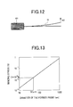
- FIG. 12 is a diagram showing the state of bending stress of the conventional probe
- FIG. 13 is a diagram showing dependency of a bending stress upon a diameter of the conventional probe relative to lateral bending of 1 ⁇ m;
- FIG. 14 is a diagram showing the state of bending stress of the probe formed at its tip with the microscopic rod.
- FIG. 15 is a diagram showing dependency of a bending stress upon a length of the microscopic rod relative to lateral bending of 1 ⁇ m.
- FIGS. 2A and 2B show probes, respectively, wherein FIG. 2A shows the conventional probe, while FIG. 2B shows the probe of this embodiment that is formed at its tip with a microscopic rod being one example of the embodiment of the present invention.
- the conventional probe 53 is in the form of a tungsten line that is formed with a sharp tip by electropolishing.
- the probe of this embodiment comprises a tungsten line 102 having a microscopic rod 103 at its tip.
- the microscopic rod 103 has a thickness of 2 ⁇ m and a length of 40 ⁇ m.
- the tungsten line 102 has a thickness of 50 ⁇ m.
- FIG. 3 shows a basic structure of a microfabrication apparatus being one example of the embodiment of the present invention.
- the microfabrication apparatus comprises a charged particle beam apparatus wherein an ion beam is extracted from an ion source 1 by an extractor 2 and, after condensing the ion beam by a condenser lens 3 , the ion beam is throttled by a beam limiting aperture 4 and then focused onto the surface of a sample 8 by an objective lens 6 , and further comprises a movable specimen stage 7 for placing thereon a sample, a secondary-particle detector 9 , a deflector 5 , a controller 10 , a nozzle for adsorbed gas 20 , and a mechanical probe 21 .
- FIG. 4 shows a method of fixing the microscopic rod 103 to the mechanical probe 21 .
- a plug 101 is fixed to the mechanical probe 21
- the tungsten line 102 is fixed to the tip of the plug 101
- the tungsten line 102 has the microscopic rod 103 at its tip.
- the tungsten line 102 is fixed to the mechanical probe 21 so as to be inclined relative to the surface of the sample 8. With this arrangement, the tip of the microscopic rod 103 can contact with the surface of the sample with no interference of the mechanical probe 21 , the plug 101 and the tungsten line 102 .
- FIGS. 5A to 5 J show a microfabrication method in this embodiment, which will be described hereinbelow along the flow.
- a posture of a sample substrate 51 is retained such that an ion beam 52 is irradiated perpendicularly onto the surface of the substrate 51 , then the ion beam 52 scans rectangularly in the neighborhood of an observation area 50 to form rectangular holes 54 having a given depth on the surface of the substrate 51 (FIG. 5 A). Then, the ion beam 52 scans rectangularly to form a trench 55 on the surface of the substrate 51 (FIG. 5 B).
- the substrate 51 is inclined such that the axis of the ion beam 52 is inclined by about 30° relative to the surface of the substrate 51 , thereby to form an inclined trench 56 .
- the posture change in inclination of the substrate 51 is implemented by the specimen stage (FIG. 5 C).
- the tip of the microscopic rod 103 is brought into contact with a portion of the substrate 51 that becomes a sample (FIG. 5 D).
- Adsorbed gas is supplied from the nozzle for adsorbed gas 20 , and the ion beam 52 is irradiated locally onto an area including the tip of the microscopic rod 103 , thereby to form an IBAD film 57 .
- the tip of the microscopic rod 103 and a sample piece 58 being a separated portion of the substrate 51 in the contacting state are connected to each other by the IBAD film 57 (FIG. 5 E). Notching is applied to a residual portion by means of an focused ion beam to cut out the separated sample piece 58 from the substrate 51 .
- the cut-out separated sample piece 58 comes into the state of being supported by the connected microscopic rod 103 (FIG. 5 F).
- the separated sample piece 58 is moved to a required portion, i.e. a sample carrier 59 in this embodiment (FIG. 5 G).
- An IBAD film 60 is formed in an area including the separated sample piece 58 and the sample carrier 59 (FIG. 5 H).
- the microscopic rod 103 is cut at a portion distanced about 2 ⁇ m from the tip thereof so as to separate the microscopic rod 103 and the separated sample piece 58 from each other (FIG. 5 I). Further, the observation area 50 in the separated sample piece 58 is formed into a membrane 61 having a thickness of about 100 nm, using an ion beam 52 . An electron beam is transmitted through the membrane 61 to carry out observation in transmission electron microscopy. Again, a separated sample piece 58 is prepared through the steps of FIGS. 5A to 5 C, and the tip of the microscopic rod 103 separated in the previous step of FIG. 5I is brought into contact with a portion of the substrate 51 that becomes a sample (FIG. 5 D).
- the separated sample piece 58 is conveyed to the sample carrier 59 through the steps of FIGS. 5E to 5 I.
- steps of FIGS. 5A to 5 I as many as ten separated sample pieces 58 can be conveyed to the sample carrier 59 without processing or replacing the microscopic rod 103 .
- microfabrication apparatus being one example of the embodiment of the present invention as shown in FIG. 3
- evaluation/analysis of semiconductor wafers was conducted.
- the microscopic rod 103 shown in FIG. 2B was changed to have a diameter of 2 ⁇ m and a length of 50 ⁇ m.
- this microscopic rod 103 one separated sample piece 58 was extracted from each of the 25 wafers. By analyzing those separated sample pieces 58 , comparison among the 25 wafers was able to be achieved. Since it was possible to extract those 25 separated sample pieces 58 without processing or replacing the microscopic rod 103 , the throughput of sample preparation was improved.
- the microscopic rod 103 shown in FIG. 2B was changed to have a diameter of 2 ⁇ m and a length of 100 ⁇ m.
- This microscopic rod 103 separated sample pieces 58 were extracted from two different portions of each of the 25 wafers.
- evaluation of uniformity within each wafer was able to be compared among the 25 wafers. Since it was possible to extract those 50 separated sample pieces 58 without processing or replacing the microscopic rod 103 , the throughput of sample preparation was improved.
- FIGS. 6A and 6B each show a method of fixing the separated sample piece 58 to the probe, wherein FIG. 6A shows a case where the conventional probe is used, while FIG. 6B shows a case where the probe formed at its tip with the microscopic rod 103 being one example of the embodiment of the present invention is used.
- a thickness 62 is about 4 ⁇ m
- a height 63 is about 20 ⁇ m
- a width 64 is about 30 ⁇ m.
- the conventional probe 53 fixes, at its sharp tip, the separated sample piece 58 with the IBAD film 57 .
- a sectional area of the microscopic rod 103 is set to 20 ⁇ m 2 or less, for example, in case of the microscopic rod 103 having a rectangular section of 4 ⁇ m ⁇ 5 ⁇ m, it is possible to fix the separated sample piece 58 using the IBAD film 57 almost satisfactorily.
- the sectional area thereof exceeds 20 ⁇ m 2 , for example, in case of the microscopic rod 103 having a rectangular section of 5 ⁇ m ⁇ 5 ⁇ m, the width of the microscopic rod 103 is greater than the thickness of the separated sample piece 58 so that fixation of the separated sample piece 58 by the IBAD film 57 becomes difficult.
- the sectional area thereof is preferably set to 20 ⁇ m 2 or less.
- FIGS. 7A and 7B each show a method of restoring the probe, wherein FIG. 7A shows a case where the conventional probe is used, while FIG. 7B shows a case where the probe formed at its tip with the microscopic rod 103 being one example of the embodiment of the present invention is used.
- the probe 53 since the sharp tip thereof is lost due to repetition of conveying the separated sample piece 58 , the probe 53 is replaced with a new one, or a restored portion 71 processed by the ion beam 52 is fixed to the separated sample piece 58 by the IBAD film 57 .
- the probe having at its tip the microscopic rod 103 of the present invention is only shortened by a length about twice its diameter upon every sample extraction and thus can repeat conveyance of the separated sample piece 58 . Therefore, it can repeat conveyance of the separated sample piece 58 about 50 times until the microscopic rod 103 is lost. If a joining portion between the tungsten line 102 and the microscopic rod 103 has a smooth conical shape, even the tip of the microscopic rod 103 that has been extremely shortened due to conveyance of the separated sample piece 58 can contact with the sample 8, so that the probe can be used for conveyance of the separated sample piece 58 until the microscopic rod 103 is shortened to the root thereof.
- FIG. 8 shows the state of resonance vibration 105 of the conventional probe 53 .
- the probe 53 shown in Embodiment 1 has a length of about 3 mm for allowing the tip thereof to contact with the sample 8 .
- the probe 53 fixed to the tip of the plug 101 largely vibrates at a frequency resonant with vibration of the plug 101 (hereinafter this frequency will be referred to as “resonance frequency”).
- FIG. 9 shows dependency of the resonance frequency upon the diameter of the probe 53 .
- the diameter of the probe 53 put to practical use is 50 to 150 ⁇ m in terms of restriction of preparation and strength. Therefore, the resonance frequency of the conventional probe 53 is 1 kHz or higher.
- FIG. 10 shows the state of resonance vibration 106 of the probe formed at its tip with the microscopic rod 103 being one example of the embodiment of the present invention.
- the microscopic rod 103 formed at the tip of the tungsten line 102 fixed to the plug 101 largely vibrates at a resonance frequency due to vibration of the plug 101 .
- FIG. 11 shows dependency of the resonance frequency upon the length of the microscopic rod 103 .
- the diameter of the microscopic rod 103 in this embodiment is 1 ⁇ m.
- the resonance frequency increases. For increasing the resonance frequency to 1 kHz or higher, it is necessary that the length of the microscopic rod 103 is about 300 ⁇ m or less.
- the length of the microscopic rod 103 is set to 300 times its diameter or less in case of the diameter being 1 ⁇ m. It is necessary that the length of the microscopic rod 103 is set to about 500 ⁇ m or less when the diameter is 2 ⁇ m, about 600 am or less when 3 ⁇ m, and about 700 ⁇ m or less when 4 82 m.
- FIG. 12 shows the state of bending stress of the conventional probe 53 .
- the length of the probe 53 is about 3 mm.
- the force 107 balances with a bending stress of the probe 53 .
- FIG. 13 shows dependency of the bending stress upon the diameter of the probe 53 when the tip of the probe 53 is bent laterally by 1 ⁇ m. Since the diameter of the probe 53 put to practical use is set to 50 to 150 ⁇ m in terms of restriction of preparation and strength, the bending stress of the probe 53 is 10 ⁇ 6 N or greater.
- the force 107 applied to the probe 53 upon sample preparation there are two kinds, i.e.
- the weight of the separated sample piece 58 is 10 ⁇ 8 g or less, while the force 107 applied to the probe 53 is 10 ⁇ 10 N or less. Therefore, there is no influence of the weight of the separated sample piece 58 to the probe 53 .
- the bending stress 10 ⁇ 6 N of the probe 53 is given as a safety strength for preventing bending caused by the force of electric field due to charge etc. during sample preparation.
- the probe 53 having a diameter of 20 ⁇ m or less with a bending stress of 10 ⁇ 8 N or greater there was a case where extraction of a sample was not achieved due to occurrence of vibration etc. due to charge during sample preparation.
- FIG. 14 shows the state of bending stress of the probe formed at its tip with the microscopic rod 103 being one example of the embodiment of the present invention.
- a force 108 is applied to the tip of the microscopic rod 103 formed at the tip of the tungsten line 102 fixed to the plug 101 , the microscopic rod 103 is bent.
- the force 108 balances with a bending stress of the microscopic rod 103 .
- FIG. 15 shows dependency of the bending stress upon the length of the microscopic rod 103 when the tip of the microscopic rod 103 is bent laterally by 1 ⁇ m.
- the length of the microscopic rod 103 is set to 100 ⁇ m or less. Therefore, for extracting the separated sample piece 58 from an insulator sample where charge etc. are generated, it is safe that the length of the microscopic rod 103 is set to 25 times its diameter or less when the diameter is 4 82 m.
- a material of a microscopic rod having a property substantially equal to dependency ( FIG. 15 ) of the bending stress shown in Embodiment 4 upon the length of the microscopic rod there are, apart from tungsten, molybdenum, beryllium, nickel and tantalum.
- the microscopic rod 103 made of a material including at least one of them had a bending stress of about 10 ⁇ 7 N when a diameter was 2 ⁇ m and a length was 100 ⁇ m, and it was possible to extract about 50 samples without being subjected to bending caused by charge of an insulator etc. during sample preparation.
- the microscopic rod 103 made of a material including at least one of palladium and osmium had a bending stress of about 10 ⁇ 7 N when a diameter was 2 ⁇ m and a length was 50 ⁇ m, and it was possible to extract about 25 samples without being subjected to bending caused by charge of an insulator etc. during sample preparation.
- the life of the probe is improved to 10 times or more in terms of the number of sample preparation enabling times, further, a sample preparation time is shortened about ten minutes by eliminating the probe restoration operation upon sample extraction, and simultaneously, the reliability of sample preparation is improved correspondingly to the elimination of the probe restoration operation and the reduction in number of times of the probe replacement.
Landscapes
- Chemical & Material Sciences (AREA)
- Analytical Chemistry (AREA)
- Physics & Mathematics (AREA)
- Engineering & Computer Science (AREA)
- Plasma & Fusion (AREA)
- Sampling And Sample Adjustment (AREA)
- Analysing Materials By The Use Of Radiation (AREA)
Applications Claiming Priority (2)
| Application Number | Priority Date | Filing Date | Title |
|---|---|---|---|
| JP2003006505A JP3996856B2 (ja) | 2003-01-15 | 2003-01-15 | 試料作製装置と試料作製方法 |
| JP2003-006505 | 2003-01-15 |
Publications (2)
| Publication Number | Publication Date |
|---|---|
| US20040135096A1 US20040135096A1 (en) | 2004-07-15 |
| US6894287B2 true US6894287B2 (en) | 2005-05-17 |
Family
ID=32588506
Family Applications (1)
| Application Number | Title | Priority Date | Filing Date |
|---|---|---|---|
| US10/603,720 Expired - Fee Related US6894287B2 (en) | 2003-01-15 | 2003-06-26 | Microfabrication apparatus and microfabrication method |
Country Status (3)
| Country | Link |
|---|---|
| US (1) | US6894287B2 (ja) |
| JP (1) | JP3996856B2 (ja) |
| FR (1) | FR2849955B1 (ja) |
Cited By (3)
| Publication number | Priority date | Publication date | Assignee | Title |
|---|---|---|---|---|
| US20100031405A1 (en) * | 2005-05-10 | 2010-02-04 | Kley Victor B | Tool Tips with Scanning Probe Microscopy and/or Atomic Force Microscopy Applications |
| US9423693B1 (en) | 2005-05-10 | 2016-08-23 | Victor B. Kley | In-plane scanning probe microscopy tips and tools for wafers and substrates with diverse designs on one wafer or substrate |
| US10042263B1 (en) | 2013-03-15 | 2018-08-07 | Victor B. Kley | In-plane scanning probe microscopy tips and tools for wafers and substrates with diverse designs on one wafer or substrate |
Families Citing this family (5)
| Publication number | Priority date | Publication date | Assignee | Title |
|---|---|---|---|---|
| JP4537827B2 (ja) * | 2003-10-27 | 2010-09-08 | エスアイアイ・ナノテクノロジー株式会社 | マニピュレータのニードル部欠陥修正方法とニードル部材セット |
| DE102008042179B9 (de) * | 2008-09-17 | 2013-10-10 | Carl Zeiss Microscopy Gmbh | Verfahren zur Analyse einer Probe |
| JP5152111B2 (ja) * | 2009-06-22 | 2013-02-27 | 新日鐵住金株式会社 | 集束イオンビーム加工装置用プローブ、プローブ装置、及びプローブの製造方法 |
| US9202672B2 (en) | 2010-04-16 | 2015-12-01 | Hitachi High-Technologies Corporation | Apparatus and method for probe shape processing by ion beam |
| CN208969129U (zh) * | 2018-09-29 | 2019-06-11 | Fei公司 | 晶片、微操纵器、用于制备微操纵器的系统 |
Citations (2)
| Publication number | Priority date | Publication date | Assignee | Title |
|---|---|---|---|---|
| US6538254B1 (en) * | 1997-07-22 | 2003-03-25 | Hitachi, Ltd. | Method and apparatus for sample fabrication |
| US6717156B2 (en) * | 2001-05-08 | 2004-04-06 | Hitachi, Ltd. | Beam as well as method and equipment for specimen fabrication |
-
2003
- 2003-01-15 JP JP2003006505A patent/JP3996856B2/ja not_active Expired - Fee Related
- 2003-06-26 US US10/603,720 patent/US6894287B2/en not_active Expired - Fee Related
- 2003-07-18 FR FR0308792A patent/FR2849955B1/fr not_active Expired - Fee Related
Patent Citations (2)
| Publication number | Priority date | Publication date | Assignee | Title |
|---|---|---|---|---|
| US6538254B1 (en) * | 1997-07-22 | 2003-03-25 | Hitachi, Ltd. | Method and apparatus for sample fabrication |
| US6717156B2 (en) * | 2001-05-08 | 2004-04-06 | Hitachi, Ltd. | Beam as well as method and equipment for specimen fabrication |
Cited By (4)
| Publication number | Priority date | Publication date | Assignee | Title |
|---|---|---|---|---|
| US20100031405A1 (en) * | 2005-05-10 | 2010-02-04 | Kley Victor B | Tool Tips with Scanning Probe Microscopy and/or Atomic Force Microscopy Applications |
| US8776261B2 (en) * | 2005-05-10 | 2014-07-08 | Victor B. Kley | Tool tips with scanning probe microscopy and/or atomic force microscopy applications |
| US9423693B1 (en) | 2005-05-10 | 2016-08-23 | Victor B. Kley | In-plane scanning probe microscopy tips and tools for wafers and substrates with diverse designs on one wafer or substrate |
| US10042263B1 (en) | 2013-03-15 | 2018-08-07 | Victor B. Kley | In-plane scanning probe microscopy tips and tools for wafers and substrates with diverse designs on one wafer or substrate |
Also Published As
| Publication number | Publication date |
|---|---|
| JP3996856B2 (ja) | 2007-10-24 |
| JP2004219236A (ja) | 2004-08-05 |
| FR2849955B1 (fr) | 2015-05-15 |
| US20040135096A1 (en) | 2004-07-15 |
| FR2849955A1 (fr) | 2004-07-16 |
Similar Documents
| Publication | Publication Date | Title |
|---|---|---|
| US6717156B2 (en) | Beam as well as method and equipment for specimen fabrication | |
| EP1998356B1 (en) | In-Situ STEM Sample Preparation | |
| CN100373532C (zh) | 用于操纵显微试样的方法和设备 | |
| US6858851B2 (en) | Apparatus for specimen fabrication and method for specimen fabrication | |
| US8723144B2 (en) | Apparatus for sample formation and microanalysis in a vacuum chamber | |
| JP5350605B2 (ja) | サンプルの作製 | |
| JP2022033241A (ja) | 試料作製装置 | |
| US6870161B2 (en) | Apparatus for processing and observing a sample | |
| JP5138294B2 (ja) | 試験片から微小サンプルを分離する方法 | |
| WO1999005506A1 (en) | Method and apparatus for preparing samples | |
| JP4205992B2 (ja) | イオンビームによる試料加工方法、イオンビーム加工装置、イオンビーム加工システム、及びそれを用いた電子部品の製造方法 | |
| US20040056194A1 (en) | Method for manipulating microscopic particles and analyzing | |
| US6894287B2 (en) | Microfabrication apparatus and microfabrication method | |
| US20230358696A1 (en) | Method for cross-section sample preparation | |
| JP2007194096A (ja) | 荷電粒子ビーム装置、及び荷電粒子ビーム装置を用いた試料のピックアップ方法 | |
| JP2014522992A (ja) | ナノマニピュレータにより保持されたサンプルの処理方法 | |
| JP4644470B2 (ja) | イオンビーム加工装置および試料作製方法 | |
| JPH07296756A (ja) | 微細加工方法およびその装置 | |
| JP4883712B2 (ja) | ウエハアース機構及び試料作製装置 | |
| JP2020057604A (ja) | 複数のリフトアウト針を含むチップ、マイクロマニピュレータ及びマイクロマニピュレータを調製するためのシステム | |
| JPH04373125A (ja) | 集束イオンビーム装置およびそれによる加工方法 | |
| JP2008122166A (ja) | 探針交換方法及び探針交換用冶具 | |
| KR20070028401A (ko) | 입자의 조성 분석 방법 | |
| CN106057617A (zh) | 在带电粒子装置的真空室中操纵样品的方法 |
Legal Events
| Date | Code | Title | Description |
|---|---|---|---|
| AS | Assignment |
Owner name: HITACHI HIGH-TECHNOLOGIES CORPORATION, JAPAN Free format text: ASSIGNMENT OF ASSIGNORS INTEREST;ASSIGNORS:FUKUDA, MUNEYUKI;TOMIMATSU, SATOSHI;SHICHI, HIROYASU;AND OTHERS;REEL/FRAME:014241/0925;SIGNING DATES FROM 20030324 TO 20030326 |
|
| FEPP | Fee payment procedure |
Free format text: PAYOR NUMBER ASSIGNED (ORIGINAL EVENT CODE: ASPN); ENTITY STATUS OF PATENT OWNER: LARGE ENTITY |
|
| FPAY | Fee payment |
Year of fee payment: 4 |
|
| FEPP | Fee payment procedure |
Free format text: PAYER NUMBER DE-ASSIGNED (ORIGINAL EVENT CODE: RMPN); ENTITY STATUS OF PATENT OWNER: LARGE ENTITY Free format text: PAYOR NUMBER ASSIGNED (ORIGINAL EVENT CODE: ASPN); ENTITY STATUS OF PATENT OWNER: LARGE ENTITY |
|
| FPAY | Fee payment |
Year of fee payment: 8 |
|
| REMI | Maintenance fee reminder mailed | ||
| LAPS | Lapse for failure to pay maintenance fees | ||
| STCH | Information on status: patent discontinuation |
Free format text: PATENT EXPIRED DUE TO NONPAYMENT OF MAINTENANCE FEES UNDER 37 CFR 1.362 |
|
| FP | Lapsed due to failure to pay maintenance fee |
Effective date: 20170517 |