US6696864B2 - Logic circuit and its forming method - Google Patents
Logic circuit and its forming method Download PDFInfo
- Publication number
- US6696864B2 US6696864B2 US10/266,773 US26677302A US6696864B2 US 6696864 B2 US6696864 B2 US 6696864B2 US 26677302 A US26677302 A US 26677302A US 6696864 B2 US6696864 B2 US 6696864B2
- Authority
- US
- United States
- Prior art keywords
- circuit
- delay time
- input
- node
- selector
- Prior art date
- Legal status (The legal status is an assumption and is not a legal conclusion. Google has not performed a legal analysis and makes no representation as to the accuracy of the status listed.)
- Expired - Fee Related
Links
Images


Classifications
-
- H—ELECTRICITY
- H03—ELECTRONIC CIRCUITRY
- H03K—PULSE TECHNIQUE
- H03K19/00—Logic circuits, i.e. having at least two inputs acting on one output; Inverting circuits
- H03K19/02—Logic circuits, i.e. having at least two inputs acting on one output; Inverting circuits using specified components
- H03K19/173—Logic circuits, i.e. having at least two inputs acting on one output; Inverting circuits using specified components using elementary logic circuits as components
- H03K19/1733—Controllable logic circuits
- H03K19/1737—Controllable logic circuits using multiplexers
-
- G—PHYSICS
- G06—COMPUTING; CALCULATING OR COUNTING
- G06F—ELECTRIC DIGITAL DATA PROCESSING
- G06F30/00—Computer-aided design [CAD]
- G06F30/30—Circuit design
- G06F30/32—Circuit design at the digital level
- G06F30/327—Logic synthesis; Behaviour synthesis, e.g. mapping logic, HDL to netlist, high-level language to RTL or netlist
Definitions
- the present invention relates to a fast logic circuit formed using selector circuits, as well as a method for forming such the logic circuit.
- CPL Complementary Pass transistor Logic
- the CPL logic circuit is composed of 2-input 1-output pass transistor selectors composed of only n-channel field-effect transistors and buffer inverters respectively.
- the most typical characteristic of the CPL is that two 2-input 1-output pass transistor selectors are always paired so as to be formed as a differential logic circuit that uses signals of both positive and negative polarities. This is different from the technology disclosed in the document 1.
- the CPL forms a fast logic circuit by taking advantage of the characteristics of both pass transistor circuit that can realize a complicated logic function with less transistors and differential circuit that requires no inverter for polarity matching. According to the document 2, the CPL has actually realized a full adder 2.5 times faster than a CMOS circuit.
- DPL Double Pass transistor Logic
- the DPL logic circuit is composed of differential pass transistor selectors so as to use signals of both positive and negative polarities.
- each pass transistor selector is composed of both n-channel and p-channel field-effect transistors.
- each selector circuit is composed of only n-channel field-effect transistors.
- each selector uses p-channel field-effect transistors together with n-channel field-effect transistors thereby avoiding such a problem of voltage drop equivalent to the threshold voltage value. Consequently, the circuit can operate fast even at a low supply voltage.
- U.S. Pat. No. 5,040,139 (hereafter, to be referred to as document 4)
- U.S. Pat. No. 5,162,666 (hereafter, to be referred to as document 5)
- U.S. Pat. No. 5,200,907 (hereafter, to be referred to as document 6) have disclosed methods for forming logic circuits using selectors composed mainly of pass transistor circuits referred to as a TGM circuit (Transmission Gate Multiplexer) respectively.
- a TGM composed mainly of pass transistor circuits can operate faster than XOR, NAND, and NOR gates composed of a CMOS circuit respectively, so a TGM based logic circuit can operate faster than any of conventional CMOS based logic circuits.
- an actual large logic circuit has a plurality of paths between an input and an output respectively. Consequently, a time required until an output signal is determined (that is, a delay time of the output signal) is decided by the delay time of a (so-called critical) path among the paths, which has the largest total delay time of its elements of a transistor circuit such as a transistor, etc. In addition, if there are a plurality of output signals, the operation speed of a logic circuit is decided by the delay time of the output signal whose delay time is the largest.
- the delay time of the entire logic circuit in such a case becomes the sum of the delay time of the circuit itself and the delay time of the input signal, which is delayed from others.
- the operation speed of the entire circuit is decided by the operation speed of the path. Consequently, if there is any input signal that is delayed extremely, the logic circuit should be formed so that the number of steps in the path related to the input signal is reduced by all means and the delay times of all the paths in the circuit become equal.
- a preferred form of the present invention is a logic circuit (C 1 shown in FIG. 1) including: the first selector (S 1 ) in which the control input S is controlled by the first input signal (IN 1 ), and the input signal I 1 or I 0 is controlled by the second input signal (IN 2 ), and the output O is connected to the first node (N 1 ); and the third selector (S 3 ) in which the control input S is controlled by the first node (N 1 ), the input I 1 is controlled by the third input signal (IN 3 ), the input I 0 is controlled by the first input signal (IN 1 ), and the output O is connected to the first output signal (OUT 1 ).
- FIG. 2 Another preferred form of the present invention is a logic circuit (C 41 shown in FIG. 2) including: the 41st selector (S 41 ) in which the control input S is controlled by the first input signal (IN 1 ), the input signal I 1 is controlled by the third input signal (IN 3 ), and the output O is connected to the 41st node (N 41 ); and the 43rd selector (S 43 ) in which the control input S is controlled by the second input signal (IN 2 ), one of the input I 1 and I 0 is controlled by the 41st node (N 41 ), the other is controlled by the first input signal (IN 1 ), and the output O is connected to the first output signal (OUT 1 ).
- FIG. 1 Further another preferred form of the present invention is a logical circuit (C 1 shown in FIG. 1) including: the first selector (S 1 ) in which the control input S is controlled by the first input signal (IN 1 ), the input I 1 is controlled by the second input signal (IN 2 ), the input I 0 is connected to a constant potential (GND), and the output O is connected to the first node (N 1 ); the second selector (S 2 ) in which the control input S is controlled by the first input signal (IN 1 ), the input I 1 is controlled by the fourth input signal (IN 4 ), the input I 0 is controlled by the fifth input signal (IN5), and the output O is connected to the second node (N 2 ); and the third selector (S 3 ) in which the control input S is controlled by the first node (N 1 ), the input I 1 is controlled by the third input signal (IN 3 ), the input I 0 is controlled by the second node (N 2 ), and the output O is connected to the first output signal (OUT 1 ).
- FIG. 1 Further another preferred form of the present invention is a logic circuit (C 21 shown in FIG. 1) including: the 21st selector (S 21 ) in which the control input S is controlled by the first input signal (IN 1 ), the input signal I 1 is connected to a constant potential (GND), and the input signal I 0 is controlled by the second input signal (IN 2 ), and the output O is connected to the 21st node (N 21 ); the 22nd selector (S 22 ) in which the control input S is controlled by the first input signal (IN 1 ), the input I 1 is controlled by the fifth input signal (IN 5 ), the input signal I 0 is controlled by the fourth input signal (IN 4 ), and the output O is connected to the 22nd node (N 22 ); and the 23rd selector (S 23 ) in which the control input S is controlled by the 21st node (N 21 ), the input I 1 is controlled by the third input signal (IN 3 ), the input I 0 is controlled by the 22nd node (N 22 ), and
- FIG. 2 Further another preferred form of the present invention is a logical circuit (C 41 shown in FIG. 2) including: the 41st selector (S 41 ) in which the control input S is controlled by the first input signal (IN 1 ), the input I 1 is controlled by the third input signal (IN 3 ), the input I 0 is controlled by the fifth input signal (IN 5 ), and the output O is connected to the 41st node (N 41 ); the 42nd selector (S 42 ) in which the control input S is controlled by the first input signal (IN 1 ), the input I 1 is controlled by the fourth input signal (IN 4 ), the input I 0 is controlled by the fifth input signal (IN 5 ), and the output O is connected to the 42nd node (N 42 ); and the 43rd selector (S 43 ) in which the control input S is controlled by the second input signal (IN 2 ), the input I 1 is controlled by the 41st node (N 41 ), the input I 0 is controlled by the 42nd node (N 42 ), and the output
- FIG. 2 Further another preferred form of the present invention is a logical circuit (C 51 shown in FIG. 2) including: the 51st selector (S 51 ) in which the control input S is controlled by the first input signal (IN 1 ), the input I 1 is controlled by the fifth input signal (IN 5 ), the input I 0 is controlled by the third input signal (IN 3 ), and the output O is connected to the 51st node (N 51 ); the 52nd selector (S 52 ) in which the control input S is controlled by the first input signal (IN 1 ), the input I 1 is controlled by the fifth input signal (IN 5 ), the input I 0 is controlled by the fourth input signal (IN 4 ), and the output O is connected to the 52nd node (N 52 ); and the 53rd selector (S 53 ) in which the control input S is controlled by the second input signal (IN 2 ), the input I 1 is controlled by the 51st node (N 51 ), the input I 0 is controlled by the 52nd node (N 52 ), and the output
- FIG. 2 Further another preferred form of the present invention is a logical circuit (C 61 shown in FIG. 2) including: the 61st selector (S 61 ) in which the control input S is controlled by the second input signal (IN 2 ), the input I 1 is controlled by the fourth input signal (IN 4 ), the input I 0 is controlled by the fifth input signal (IN 5 ), and the output O is connected to the 61st node (N 61 ); the 62nd selector (S 62 ) in which the control input S is controlled by the third input signal (IN 3 ), the input I 1 is controlled by the fourth input signal (IN 4 ), the input I 0 is controlled by the fifth input signal (IN 5 ), and the output O is connected to the 62nd node (N 62 ); and the 63rd selector (S 63 ) in which the control input S is controlled by the first input signal (IN 1 ), the input I 1 is controlled by the 61st node (N 61 ), the input I 0 is controlled by
- FIG. 2 Further another preferred form of the present invention is a logical circuit (C 71 shown in FIG. 2) including: the 71st selector (S 71 ) in which the control input S is controlled by the third input signal (IN 3 ), the input I 1 is controlled by the fourth input signal (IN 4 ), the input I 0 is controlled by the fifth input signal (IN 5 ), and the output O is connected to the 71st node (N 71 ); the 72nd selector (S 72 ) in which the control input S is controlled by the first input signal (IN 1 ), the input I 1 is controlled by the fourth input signal (IN 4 ), the input I 0 is controlled by the 71st node (N 71 ), and the output O is connected to the 72nd node (N 72 ); the 73rd selector (S 73 ) in which the control input S is controlled by the first input signal (IN 1 ), the input I 1 is controlled by the fifth input signal (IN 5 ), the input I 0 is controlled by the 71st
- FIG. 2 Further another preferred form of the present invention is a logical circuit (C 81 shown in FIG. 2) including: the 81st selector (S 81 ) in which the control input S is controlled by the second input signal (IN 2 ), the input I 1 is controlled by the fourth input signal (IN 4 ), the input I 0 is controlled by the fifth input signal (IN 5 ), and the output O is connected to the 81st node (N 81 ); the 82nd selector (S 82 ) in which the control input S is controlled by the first input signal (IN 1 ), the input I 1 is controlled by the 81st node (N 81 ), the input I 0 is controlled by the fourth input signal (IN 4 ), and the output O is connected to the 82nd node (N 82 ); the 83rd selector (S 83 ) in which the control input S is controlled by the first input signal (IN 1 ), the input I 1 is controlled by the 81st node (N 81 ), the input I 0
- FIG. 1 Further another preferred embodiment of the present invention is logic circuits C 1 , C 11 , C 21 , and C 31 shown in FIG. 1 and logic circuits C 41 , C 51 , C 61 , C 71 , and C 81 shown in FIG. 2 including respectively a selector (C 100 shown in the a-row in FIG.
- FIG. 1 Further another preferred embodiment of the present invention is logic circuits C 1 , C 11 , C 21 , and C 31 shown in FIG. 1 and logic circuits C 41 , C 51 , C 61 , C 71 , and C 81 shown in FIG. 2 including respectively a selector (C 200 shown in the a-row in FIG.
- FIG. 4 Further another preferred embodiment of the present invention is a logic circuit (C 120 shown in FIG. 4 ), which includes: the 127th p-channel field-effect transistor (TP 127 ) in which the gate is controlled by the first input signal (IN 1 ) and a source drain path is connected between the first operation potential point (VDD) and the 127th node (N 127 ); the 127th n-channel field-effect transistor (TN 127 ) in which the gate is controlled by the first input signal (IN 1 ) and a source drain path is connected between the second operation potential point (GND) and the 127th node (N 127 );
- FIG. 4 Further another preferred embodiment of the present invention is a logic circuit (C 120 shown in the a-row in FIG. 4 ), which includes: the 120th p-channel field-effect transistor (TP 120 ) in which the gate is controlled by the first input signal (IN 1 ) and a source drain path is connected between the first operation potential point (VDD) and the 120th node (N 120 );
- FIG. 5 Further another preferred embodiment of the present invention is a logic circuit (C 140 shown in the a-row in FIG. 5 ), which includes: the 140th p-channel field-effect transistor (TP 140 ) in which the gate is controlled by the first input signal (IN 1 ) and a source drain path is connected between the first operation potential point (VDD) and the 140th node (N 140 ); the 140th n-channel field-effect transistor (TN 140 ) in which the gate is controlled by the first input signal (IN 1 ) and a source drain path is connected between the second operation potential point (GND) and the 140th node (N 140 );
- the 145th n-channel field-effect transistor (TN 145 ) in which the gate is controlled by the 141st node (N 141 ) and a source drain path is connected between the third input signal (IN 3 ) and the 145th node (N 145 );
- the 146th n-channel field-effect transistor (TN 146 ) in which the gate is controlled by the 150th node (N 150 ) and a source drain path is connected between the 144th node (N 144 ) and the 145th node (N 145 );
- the 148th n-channel field-effect transistor (TN 148 ) in which the gate is controlled by the 147th node (N 147 ) and a source drain path is connected between the second input signal (IN 2 ) and the 148th node (N 148 );
- the 149th n-channel field-effect transistor (TN 149 ) in which the gate is controlled by the first input signal (IN 1 ) and a source drain path is connected between the first operation potential point (VDD) or the second operation potential point (GND) and the 148th node (N 148 );
- FIG. 11 Further another preferred embodiment of the present invention is a logic circuit (C 160 shown in the a-row in FIG. 11 ), which includes: the 160th p-channel field-effect transistor (TP 160 ) in which the gate is controlled by the first input signal (IN 1 ) and a source drain path is connected between the first operation potential point (VDD) and the 160th node (N 160 ); the 160th n-channel field-effect transistor (TN 160 ) in which the gate is controlled by the first input signal (IN 1 ) and a source drain path is connected between the second operation potential point (GND) and the 160th node (N 160 );
- the 163rd n-channel field-effect transistor (TN 163 ) in which the gate is controlled by the 160th node (N 160 ) and a source drain path is connected between the fifth input signal (IN 5 ) and the 163rd node (N 163 );
- FIG. 12 Further another preferred embodiment of the present invention is a logic circuit (C 180 shown in the a-row in FIG. 12 ), which includes: the 184th p-channel field-effect transistor (TP 184 ) in which the gate is controlled by the first input signal (IN 1 ) and a source drain path is connected between the first operation potential point (VDD) and the 185th node (N 185 ); the 185th p-channel field-effect transistor (TP 185 ) in which the gate is controlled by the second input signal (IN 2 ) and a source drain path is connected between the first operation potential point (VDD) and the 185th node (N 185 ); the 184th n-channel field-effect transistor (TN 184 ) in which the gate is controlled by the second input signal (IN 2 ) and a source drain path is connected between the 185th node (N 185 ) and the 184th node (N 184 ); the 185th n-channel field-effect transistor (TN 185 ) in which the
- FIG. 1 shows an embodiment of the present invention.
- FIG. 2 shows another embodiment of the present invention.
- FIG. 3 is a circuit diagram of a selector.
- FIG. 4 shows another embodiment of the present invention.
- FIG. 5 shows another embodiment of the present invention.
- FIG. 6 shows patterns of a selector converted to a NAND gate, a NOR gate, and an inverter respectively, as well as the conversion rules.
- FIG. 7 is a circuit diagram of a logic circuit C 1 of the present invention shown in FIG. 1, in which the selector S 1 is replaced with a NAND gate + an inverter in accordance with the convertation rules shown in the a-row in FIG. 6 .
- FIG. 8 shows redundant selectors.
- FIG. 9 shows a NAND gate, a NOR gate, and an inverter composed of a differential circuit respectively.
- FIG. 10 shows logic circuits C 1 , C 11 , C 21 , and C 31 of the present invention shown in FIG. 1, in each of which some selectors are replaced with CMOS gates in accordance with the convertation rules shown in FIG. 6 and each of those logic circuits composed of a differential circuit.
- FIG. 11 shows transistor circuit diagrams of the logic circuits C 2 and C 3 of the present invention shown in the a-row in FIG. 10 .
- FIG. 12 shows circuit diagrams of the logic circuits C 2 and C 3 of the present invention shown in the a-row in FIG. 10, from each of which redundant selectors are removed when the input signals IN 5 and IN 4 are fixed at GND and VDD respectively.
- FIG. 13 shows a circuit diagram of the logic circuit C 0 shown in the b-row in FIG. 1, in which the control input S of the selector S 5 is connected to an inverted signal of the input signal IN 2 .
- FIG. 14 shows the outline of a delay time improvement program, which uses selectors, and a computer system used to execute the delay time improvement program in the fifth embodiment of the present invention.
- FIG. 15 is a flowchart indicating processes for producing an LSI circuit started at a logic circuit specification using the delay time improvement program, which uses the logic circuits of the present invention.
- FIG. 16 is a flowchart indicating an execution of the delay time improvement program using the logic circuits of the present invention.
- FIG. 17 illustrates a forward delay time, a reverse delay time, a slack and a hole in the fifth embodiment of the present invention.
- FIG. 18 is an example of a logic circuit to be entered to the delay time improvement program, which uses the logic circuit of the present invention shown in FIG. 16 .
- FIG. 19 is a circuit diagram of a logic circuit composed of only selectors generated with a selector circuit conversion routine of the delay time improvement program, which uses the logic circuit of the present invention shown in FIG. 16 .
- FIG. 20 is a circuit diagram of an intermediate circuit generated in the middle of an execution of the delay time improvement routine of the delay time improvement program, which uses the logic circuit of the present invention shown in FIG. 16 .
- FIG. 21 is a circuit diagram of an intermediate circuit generated at a middle of an execution of the delay time improvement routine of the delay time improvement program, which uses the logic circuit of the present invention shown in FIG. 16 .
- FIG. 22 is a circuit diagram of an intermediate circuit generated at a middle of an execution of the delay time improvement routine of the delay time improvement program, which uses the logic circuit of the present invention shown in FIG. 16 .
- FIG. 23 is a circuit diagram of a circuit output finally by the delay time improvement routine of the delay time improvement program, which uses the logic circuit of the present invention shown in FIG. 16 .
- FIG. 24 is a circuit diagram of a circuit generated in the middle of an execution of the CMOS cell re-mapping routine of the delay time improvement program, which uses the logic circuit of the present invention shown in FIG. 16 .
- FIG. 25 is a circuit diagram of a circuit output finally by the CMOS cell re-mapping routine of the delay time improvement program, which uses the logic circuit of the present invention shown in FIG. 16 .
- FIG. 26 is a circuit diagram of a circuit (composed of differential selectors) output finally by the CMOS cell re-mapping routine of the delay time improvement program, which uses the logic circuit of the present invention shown in FIG. 16 .
- FIG. 27 shows results of comparison performed for a large scale logic circuit between before and after an execution of the delay time improvement program, which uses the logic circuit of the present invention shown in FIG. 16, with respect to the number of paths breaking a predetermined tolerance.
- FIG. 28 shows results of comparison performed for a large scale logic circuit between before and after an execution of the delay time improvement program, which uses the logic circuit of the present invention shown in FIG. 16, with respect to a distribution of cell holes.
- each of the selectors (S 5 and S 6 of C 0 and S 1 to S 3 of C 1 , etc.) shown in the a-row in FIG. 1 has a logic function shown with a Boolean expression (E 100 in the a-row) in FIG. 3 .
- E 100 in the a-row a Boolean expression
- this 2-input 1-output selector is composed of various types of circuits.
- the circuit C 100 has a selector part (transistors T 100 and T 101 ) composed only of n-channel field-effect transistors.
- the circuit C 100 is shown in the reference document 1.
- transistors T 102 , T 103 , and T 106 are inserted as buffers so as to be used mainly for reducing the delay time of the circuit. These transistors are omissible if another selector circuit is provided in the following stage.
- the selector part is composed, for example, of both n-channel field-effect transistors and p-channel field-effect transistors. Unlike the circuit C 100 , no voltage drop equivalent to the threshold voltage value occurs in the selector part (T 110 to T 113 ) in this circuit. Thus, even when the supply voltage is low, the circuit can operate fast.
- the circuit C 102 shown in the a-row in FIG. 3 is composed of a CMOS circuit. As understood from this case, generally, a compact selector circuit can be formed more easily if it is composed of a pass transistor circuit.
- This circuit has the following paths:
- the path of IN 3 ⁇ S 5 ⁇ N 5 ⁇ S 6 ⁇ OUT 1 shown with a thick line becomes a critical path having the largest delay time in the circuit C 0 shown in FIG. 1 .
- the delay time of the entire circuit C 0 becomes 2.0 ns, which is none other than the delay time of this critical path, although other paths can operate faster than 2.0 ns.
- the path between this IN 3 and an output has two selectors (S 5 and S 6 ) disposed in two stages, while IN 3 is delayed from other input signals in this circuit C 0 .
- the delay time of this path becomes extremely large (1.0 ns larger than those of other paths in this case), so that the delay time of the entire circuit also becomes large.
- the delay time of each path will be estimated as follows.
- the path between IN 3 and OUT 1 becomes a critical path having the largest delay time.
- the circuit C 1 can operate faster than the circuit C 0 by 0.5 ns, that is, 25% up.
- the circuits C 0 and C 1 shown in FIG. 1 have the same Boolean expression as shown below, so it is proved that both of the circuits C 0 and C 1 have the same logic function.
- the Boolean expression of the circuit C 0 will be as shown below in accordance with the notation of the Boolean expression (E 100 in FIG. 3) represented for a 2-input 1-output selector circuit.
- the circuit C 0 should be replaced with the logic circuit (C 1 ) of the present invention. Then, the number of steps will be reduced in the path between IN 3 and OUT 1 , so that the circuit can operate faster.
- circuit C 1 is represented as a transistor circuit after the selector is composed of a C 100 type circuit shown in FIG. 3, the circuit will become like C 120 shown in the a-row in FIG. 4, wherein the circuit is composed of transistors TN 120 to TN 130 , as well as TP 120 to TP 130 .
- each delay time is estimated premising that the delay time between the control input S and the output O of a selector is equal to the delay time between the signal input I 0 or I 1 and the output O.
- a selector is composed of any of circuits C 100 to C 102 shown in the a-row in FIG. 3, however, the delay time from the control input is increased according to the delay time of the internal polarity inverter (e.g., T 104 to T 105 in C 100 ).
- the delay time from any of the signal inputs I 1 and I 0 is 0.3 ns.
- the delay time from the control input S becomes 0.5 ns or so.
- a pass transistor selector is composed of a differential circuit shown as C 200 and C 201 in FIG. 3, however, the polarity inverter is omissible. Because, signals in such a differential circuit always make a pair of positive and negative polarities.
- the delay time from the control input S is reduced significantly. Concretely, the delay time becomes almost the same as the delay time from any of the signal inputs I 1 and I 0 or it becomes a little smaller than the delay time from any of the I 1 and I 0 . If a logic circuit of the present invention is composed of a differential pass transistor circuit, therefore, the circuit will further be faster in operation.
- the selector part is composed of only n-channel field-effect transistors.
- the circuit is called a CPL, which is proposed in the reference document 2.
- transistors T 204 to T 209 in this circuit C 200 are used as buffer circuits. They are omissible if another selector is provided in the next stage.
- the selector part is composed of both n-channel and p-channel field-effect transistors. This circuit can operate fast just like the circuit C 101 shown in the a-row in FIG. 3 even when the supply power is low.
- This circuit C 1 can be composed of a differential selector C 200 shown in FIG. 3 so as to be converted to the circuit C 220 shown in the b-row in FIG. 4, wherein the circuit is composed of transistors TN 220 to TN 235 , as well as TP 220 to TP 235 .
- the circuit will operate faster, because no polarity inverter is needed in the control input part of the selector.
- circuit characteristics including delay time, etc. are often improved furthermore if one of the two inputs I 0 and I 1 is fixed at GND or VDD and the pass transistor selectors (selectors S 300 to S 330 shown in the a-row to the d-row in FIG. 6 ), which function as an AND logic gate or an OR logic gate respectively, are replaced with a NAND gate, a NOR gate, etc. (G 300 to G 331 shown in the a-row to the d-row in FIG. 6) composed of a CMOS circuit having equivalent logic functions. (For example, refer to Proceeding of 1997 The Symposium on VLSI circuits (pp.31-32).
- the NAND gate, the NOR gate, and the inverter indicated as G 300 to G 331 in FIG. 6 are composed of a standard CMOS circuit indicated as G 340 (transistors T 340 to T 343 ), G 350 (transistors T 350 to T 353 ), and G 360 (transistors T 360 to T 363 ) respectively.
- the selector S 1 is equivalent to the selector S 300 shown in the a-row in FIG. 6 .
- the circuit C 1 can thus be replaced with a NAND gate + an inverter (refer to the conversion pattern in the a-row in FIG. 6 ).
- the circuit C 1 can thus be converted to the circuit shown in FIG. 7 .
- the operations of the inverter G 2 and the selector S 3 in the circuit shown in FIG. 7 if “1” is entered to the inverter G 2 , “0” is entered to the control input of the selector S 3 .
- the selector thus selects I 1 . If “0” is entered to the inverter G 2 , “1” is entered to the control input of the selector S 3 .
- the selector S 3 thus selects I 0 .
- the delay time of a 2-input NAND gate (G 1 ) is smaller than the delay time of a selector. If the delay time of a selector is 0.5 ns or so, for example, the delay time of a 2-input NAND gate (G 1 ) is 0.2 ns or so.
- the delay time of this circuit C 2 can be estimated as follows:
- the delay time of the critical path becomes 1.5 ns, which is the same as that of the circuit C 1 .
- this circuit C 2 is faster in operation in a case in which both IN 3 and IN 2 are delayed together.
- the path 5 thus becomes a critical path.
- the delay time of 1.5 ns makes the circuit C 1 delay in operation by 0.1 ns, which disables the operation of the circuit C 1 itself.
- the path 4 thus remains to be a critical path.
- the circuit operation is thus enabled within a delay time of 1.5 ns.
- this circuit C 2 could be represented as a transistor circuit C 160 as shown in the a-row in FIG. 11, wherein the circuit C 2 is composed of transistors TN 160 to TN 168 , as well as TP 160 to TP 168 .
- the logic circuit operation can further become faster by combining the selector with a CMOS circuit.
- the NAND gate G 1 in the circuit C 2 shown in FIG. 10 is equivalent to the circuit shown in the a-row in FIG. 9, so it is only needed to replace it with the NAND gate and a NOR gate in this case.
- the circuit C 2 shown in the a-row in FIG. 10 can be replaced with a differential circuit such way, thereby to obtain the circuit C 3 shown in the a-row in FIG. 10 .
- the delay time of the circuit C 3 is estimated assuming that the delay time of the path between any of the selector signal inputs I 1 and I 0 and the output O is 0.3 ns, the delay time from the control input S is 0.2 ns, and the delay time of any of the NAND and NOR gates is 0.3 ns, then the result will be as shown below.
- the circuit operation can further become faster than the circuits C 1 and C 2 . If each selector is composed of a C 200 type circuit shown in FIG. 3 in this circuit C 3 , the circuit (transistor circuit) will be converted to a circuit composed of transistors TN 260 to TN 273 , as well as TP 260 to TP 273 . The circuit is shown as C 260 in the b-row in FIG. 11 .
- the selector S 1 of the circuit C 2 is set so that I 0 and I 1 are fixed at GND and VDD respectively.
- the selector is thus equivalent to the selector S 403 shown in the c-row in FIG. 8 .
- the operation of this selector S 1 is as follows; if the control input S is “0”, a GND potential, that is, “0” is output and if the control input S is “1”, a VDD potential, that is, “1” is output.
- This selector is thus redundant and can be removed.
- the selector can also be simplified into a circuit shown as C 181 in the a-row in FIG. 12 .
- This circuit C 181 has not a path of IN 1 ⁇ S 2 ⁇ S 3 ⁇ OUT 1 , which exists in the circuit C 2 , so the circuit C 191 can operate faster than the circuit C 2 .
- selectors S 402 to S 406
- those selectors can be removed to simplify the logic circuit for faster operation.
- the circuit C 181 is composed of a C 100 type selector shown in FIG. 3, the circuit C 181 is converted to C 180 shown in FIG. 12 .
- the circuit C 180 is composed of transistors TN 180 to TN 185 , as well as TP 180 to TP 185 .
- this circuit C 181 is replaced with a differential circuit, the circuit C 181 will function like the circuit C 281 shown in the b-row in FIG. 12 .
- This circuit could be represented as a transistor circuit C 280 shown in FIG. 12 .
- the path of IN 3 ⁇ S 5 ⁇ N 5 ⁇ S 6 ⁇ OUT 1 is assumed to be a critical path in the circuit C 0 shown in FIG. 1 .
- the path of IN 4 ⁇ S 5 ⁇ N 5 ⁇ S 6 ⁇ OUT 1 is assumed to be a critical path that decides the delay time of the entire circuit (C 10 in FIG. 1 ).
- the critical path is the input I 0 in the selector S 5 in the preceding stage and the input I 1 in the selector S 6 in the following stage in this embodiment.
- This circuit C 10 is equivalent logically to the circuit shown in FIG. 13 (in which the signal of the control input S of the selector S 5 is inverted) if in accordance with the conversion rules shown in the a-row in FIG. 8 .
- reducing the number of steps in the path of IN 4 ⁇ S 5 ⁇ N 5 ⁇ S 6 ⁇ >OUT 1 is the same as reducing the number of steps in the path of IN 3 ⁇ S 5 ⁇ N 5 ⁇ S 6 ⁇ OUT 1 in the circuit C 0 shown in FIG. 1 in the first embodiment.
- the circuit C 10 can be converted to the circuit C 11 , which has the same logic function as that of the circuit C 10 . And, the number of steps in the path between IN 4 and OUT 1 can be reduced up to only one. If the logic circuit of the present invention is used as described above, therefore, the delay circuit of the circuit can be minimized.
- the selector S 11 in this circuit C 11 is equivalent to the selector S 300 shown in the a-row in FIG. 6, the selector S 11 can be replaced with a NAND gate just like in the first embodiment. In this case, the selector S 11 functions like the circuit C 12 shown in FIG. 10 .
- This circuit C 12 can also be converted to a faster one if it is replaced with a differential circuit (C 13 shown in FIG. 10) just like in the first embodiment. Especially, if the circuit C 13 shown in FIG. 10 is replaced with a differential circuit, the inverter is omissible, although the inverter had to be inserted in the circuit C 12 to invert the signal IN 2 . The circuit operation can thus be speeded up by the delay time of the inverter.
- the logic circuit of the present invention in the first embodiment can apply to the circuit C 20 if the control input IN 1 of the selector S 26 is inverted. It is also possible to convert the circuit C 20 to the circuit C 21 shown in the c-row in FIG. 1 .
- this circuit C 21 is represented as a transistor circuit composed of a selector shown as C 100 in FIG. 3, the circuit will be as shown in FIG. 5 (C 140 in the a-row).
- the circuit C 140 in FIG. 5 is composed of transistors TN 140 to TN 150 , as well as TP 140 to TP 150 .
- the circuit C 21 is composed of a differential selector shown as C 200 in FIG. 3, the circuit will be converted to C 240 shown in the b-row in FIG. 5 .
- the circuit C 240 is composed of transistors TN 240 to TN 254 , as well as TP 240 to TP 254 . Since the selector S 21 in this circuit C 21 is equivalent to the selector C 320 shown in the c-row in FIG. 6, it is possible to replace the selector S 21 with a CMOS gate (C 22 shown in the c-row in FIG. 10 ). And, the selector S 21 can be replaced with a differential circuit (C 23 shown in the c-row in FIG. 10) to reduce the delay time further.
- the input I 0 is an object path (IN 4 ⁇ S 25 ⁇ N 25 ⁇ S 26 ⁇ OUT 1 ) whose delay time should reduced in the selectors (S 25 ) and (S 26 ) in both preceding and following stages just like in the circuit C 30 shown in the d-row in FIG. 1 .
- the IN 2 can be inverted in the circuit C 20 to convert the circuit C 20 to C 31 shown in the d-row in FIG. 1 .
- the selector S 31 is equivalent to the selector S 320 shown in the c-row in FIG. 6 .
- the selector S 31 can thus be replaced with a CMOS gate (C 32 in the d-row in FIG. 10 ).
- the selector S 31 can be replaced with a differential circuit (C 33 in the d-row in FIG. 10) to reduce the delay time further.
- the input I 0 or I 1 of the preceding or following stage selector is an object path whose delay time should be reduced in a circuit including two selectors connected serially (a- to d-rows in FIG. 1) in two stages
- using the logic circuits (C 1 , C 11 , C 21 , and C 31 ) of the present invention will be effective to reduce the number of steps in the critical path, as well as the delay time of the circuit.
- control input S in the preceding stage selector (S 45 ) and the input I 1 in the following stage selector (S 46 ) are the object paths (IN 2 ⁇ S 45 ⁇ N 45 ⁇ S 46 ⁇ OUT 1 ) whose delay time should be reduced respectively as shown in the circuit C 40 in the a-row in FIG. 2 .
- the logic circuit C 41 shown in FIG. 2 of the present invention which has the same logical function as that of the circuit C 40 , is used, it is possible to reduce the number of steps in the path between IN 2 and OUT 1 up to one step composed of only the selector S 43 , as well as reduce the delay time of the entire circuit.
- the circuits C 40 and C 41 have the same logical function, since the Boolean expressions of those circuits are the same in pattern as shown below.
- the Boolean expression of the circuit C 40 is as shown below.
- the input I 0 of the following stage selector (S 46 ) is a critical path (IN 2 ⁇ S 55 ⁇ N 55 ⁇ S 56 -OUT 1 ) shown as C 50 in the b-row in FIG. 2 .
- the IN 1 in the circuit C 40 is regarded to be inverted, so it is possible to reduce the number of steps in the path using the circuit C 51 shown in the b-row in FIG. 2 .
- the logic circuit of the present invention can be used such way to reduce the delay time of the circuit in this case.
- any of the circuits (C 41 and C 51 ) in this embodiment if there are selectors equivalent to the selectors S 300 to S 330 shown in the a- to d-rows in FIG. 6, those selectors can be replaced with CMOS gates to compose an object circuit. And, each of those selectors can be replaced with a differential circuit to reduce the delay time further.
- control input S in the preceding stage selector and the input I 0 or I 1 in the following stage selector are the object paths whose delay time should be reduced respectively in a circuit including two selectors connected serially in two stages
- using the logic circuits (C 41 and C 51 ) of the present invention will be effective to reduce the number of steps in the critical path, as well as reduce the delay time of the entire circuit.
- the control input S of both preceding and following stage selectors (S 65 ) and (S 66 ) is an object path whose delay time should be reduced (IN 1 ⁇ S 65 ⁇ N 65 ⁇ S 66 ⁇ OUT 1 ) in the circuit C 60 shown in the c-row in FIG. 2 in this third embodiment.
- using the logic circuit of the present invention, shown as C 61 in FIG. 2 and having the same logic function as that of the circuit C 60 will be effective to reduce the number of steps in the object path up to only one step (IN 1 ⁇ S 63 ⁇ OUT 1 ). Consequently, it is also possible to reduce the delay time of the entire circuit.
- the circuits C 60 and C 61 are equivalent to each other logically just like in the second embodiment. This can be proved as shown below through the use of the Shannon expansion introduced in the document 8.
- the Boolean expression of the circuit C 60 will be as shown below.
- This expression matches with the Boolean expression represented for the circuit C 61 .
- the logic circuit (C 61 ) of the present invention can also be used to reduce the number of steps in the object path, as well as the delay time of the entire circuit even when the control input S is the object path whose delay time should be reduced in the selectors in both preceding and following stages in a circuit including two selectors connected serially in two stages.
- the input I 1 in the preceding stage selector (S 75 ) and the control input S in the following stage selector (S 76 ) are the object paths (IN 2 ⁇ S 75 ⁇ N 75 ⁇ S 76 ⁇ OUT 1 ) whose delay time should be reduced respectively in this fourth embodiment.
- the path is shown as C 70 in the d-row in FIG. 2 .
- the logic circuit of the present invention which is shown as C 71 in the c-row in FIG. 2, is effective.
- this circuit C 71 of the present invention can reduce the number of steps more in the object path between IN 2 and OUT 1 ; from two to one.
- the number of steps in the path between IN 4 and OUT 1 increases from one to three.
- the circuits C 70 and C 71 are the same logically just lie in the second and third embodiments. This can be proved as shown below through the use of Shannon expansion.
- the Boolean expression of the circuit C 70 will as be shown below.
- This expression matches with the Boolean expression represented for the circuit C 71 .
- the input I 0 in the preceding stage selector (S 75 ) is the object path (IN 3 ⁇ S 75 ⁇ S 76 ⁇ OUT 1 ) whose delay time should be reduced unlike the circuit C 70 .
- the path is shown as C 80 in the e-row in FIG. 2 .
- the IN 1 in the circuit C 70 is inverted. It is thus possible to replace the circuit C 80 with the circuit C 81 shown in the e-row in FIG. 2 thereby to reduce the number of steps in the object path up to one step (IN 3 ⁇ OUT 1 ).
- using the logical circuit of the present invention makes it possible to reduce the number of steps in the critical path, as well as the delay time of the entire circuit in this embodiment.
- CMOS logic circuit can be converted to a logic circuit with less delay time if it is replaced with a selector circuit, which is equivalent to the CMOS logic circuit logically, then replaced with a logic circuit of the present invention in units of selector circuits in two stages.
- description will be made for how to reduce a delay time of a more complicated logic circuit using the logic circuits of the present invention and a computer system shown in FIG. 14 .
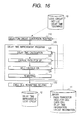
- FIG. 15 shows a schematic structure of a delay time improvement program 100 , which uses the logic circuits of the present invention and a computer system used to execute the delay time improvement program.
- This computer system comprises an input unit such as a keyboard 1 , a central processing unit (CPU) 2 , a display unit (CRT) 3 , a magnetic tape unit 4 , and a magnetic disk unit 5 used to store the delay time improvement program 100 , which uses selectors.
- the program 100 includes a selector circuit conversion routine 110 , a delay time improvement routine 120 , and a CMOS cell re-mapping routine 130 .
- This program 100 is loaded into the CPU 2 from the magnetic disk unit and executed when a designer enters an instruction from the keyboard 1 . How much a delay time is reduced is displayed on the CRT 3 and a generated delay time improvement logic circuit is passed to an automatic layout program 160 shown in FIG. 15 via the magnetic tape unit 4 , etc.
- logic circuit specifications 9 include logic functions respective logic circuits, as well as such information as delay time tolerance, etc. for delay times of input and output signals of the respective logic circuits.
- An automatic logic circuit design program 90 generates a logic circuit 10 from the logic circuit specifications 9 with reference to a library 11 .
- the logic circuit 10 contains a net list describing relationships of wiring among cells and the delay time tolerance information described above.
- the delay time improvement program 100 which uses selectors specific to this embodiment, outputs the delay time improvement logic circuit 12 provided with the same logic function as that of the logic circuit 10 with reference to the library 11 according to the information described in the logic circuit 10 so as to satisfy an object delay time tolerance.
- An automatic layout program 160 decides a layout optimized to this logic circuit with reference to the library 11 and creates layout data 20 .
- a mask data generation program 170 decides a plurality of mask patterns used to generate the logic circuit designed above using LSI circuit technologies thereby generating mask data 21 representing those mask patterns.
- An LSI production apparatus 180 produces LSI circuits provided with object logic functions respectively using the mask data 21 .
- Each of the programs 90 , 100 , 160 , and 170 is executed on a computer assigned only to itself; one computer is assigned only to one program. Of course, those programs can also be executed in the same computer.
- Each of the automatic logic circuit design program, the automatic layout program, and the mask data generation program can be created using existing tools.
- This embodiment is characterized as follows; In order to reduce a delay time of a logic circuit, an entered logic circuit is replaced with a selector circuit equivalent to the entered logic circuit logically, then the circuit in a critical path is replaced with a logic circuit of the present invention in units of selectors in two stages.
- description will be made for each routine executed in this embodiment using the logic circuit shown in FIG. 18 as an example.
- This routine 110 generates a logic circuit composed of selector circuits from the logic circuit 10 so that the generated logic circuit is provided only with the same logic function as that of the logic circuit 10 according to the conversion pattern shown in FIG. 6 .
- the conversion pattern shown in the a-row in FIG. 6 is applicable for the 2-input AND gates G 500 , G 502 , G 504 , and G 506 and the conversion pattern shown in the b-row in FIG. 6 is applicable for the rest 2-input OR gates G 501 , G 503 , and G 505 .
- the circuit is thus converted to a logic circuit composed only of the selectors shown in FIG. 1 .
- This routine re-maps logic circuits generated with the selector circuit conversion routine 110 in (2) partially in order using the logic circuits of the present invention described in the first to fourth embodiments thereby converting a given logic circuit so as to satisfy an object delay time tolerance.
- a forward delay time is defined as a value obtained by adding the delay time of an input signal to the delay time of each cell existing on an object path as shown in the expression 1 of E 400 shown in FIG. 17 .
- a delay time corresponds to a time required until a signal is transmitted to the node.
- the forward delay time thus becomes 1 ns.
- the forward delay time of this node is defined to be 2 ns, since the delay time is assumed to be the time (2 ns) obtained by adding the delay time (1 ns) of the cell G 401 to the forward delay time (1 ns) of the node N 400 or the time (1 ns) obtained by adding the delay time (1 ns) of the cell G 401 to the forward delay time (0 ns) of the node N 405 , whichever is later.
- a reverse delay time is defined as a value obtained by subtracting the delay time of each cell existing on an object path sequentially from the tolerance of output signals as shown in the expression 2 of E 400 in FIG. 17 .
- a reverse delay time corresponds to the delay time required at each node, since each output signal is determined within a predetermined delay time tolerance. For example, in order to determine an output signal OUT at a delay time tolerance of 2 ns in the circuit shown in FIG. 17, the signal must be transmitted to the node N 401 within a delay time of 1 ns, which is faster than that by the delay time (1 ns) of the cell G 402 . The reverse delay time of the node N 401 thus becomes 1 ns. As for the node N 400 , the object signal must be determined more faster by the reverse delay time (1 ns) of the node N 401 . The reverse delay time of this node thus becomes 0 ns.
- a slack is calculated from those values in the next process 122 .
- a slack is defined by a value obtained by subtracting a forward delay time from a reverse delay time as shown in the expression 3 of E 400 in FIG. 17 . If a slack of each node is calculated in this circuit shown in FIG. 17, the results will be as shown below.
- a reverse delay time corresponds to a delay time of an output signal at a node, which is needed for determining the output signal just at a predetermined delay time tolerance.
- a forward delay time corresponds to a time required until a signal is transmitted to the node.
- the critical path is N 403 ⁇ G 400 ⁇ N 400 ⁇ G 401 ⁇ N 401 ⁇ G 402 ⁇ N 402 whose slack is ⁇ 1 ns. And the critical path decides the delay time of this entire circuit.
- a cell hole is defined by the minimum difference value of the slacks found from among input terminals with respect to the nodes to which the input terminals are connected as shown in the expression of E 400 in FIG. 17 . Since a slack corresponds to a delay time allowance of each node as described above, a cell, when having a large hole value, means that the delay time of only one of a plurality of input terminals is far larger than those of other input terminals.
- the use of the logic circuits of the present invention makes it possible to re-map each circuit thereby to reduce the number of steps in each critical path and the delay time of an entire circuit without fail. In this case, however, the number of steps and the delay time may be increased in other paths sometimes.
- G 400 0 ns (difference of slack between N 403 and N 404 )
- G 401 1 ns (difference of slack between N 400 and N 405 )
- G 402 2 ns (difference of slack between N 401 and N 406 )
- each of the cells G 402 and G 401 has holes in this circuit shown in FIG. 17 . And, if the circuit composed of those G 402 and G 401 is re-mapd properly, it is possible to convert the circuit to a faster one.
- each of the cells S 505 and S 506 are largest as shown above.
- the part composed of those cells S 505 and S 506 can be replaced with a logic circuit of the present invention thereby to surely reduce the delay time of the entire circuit.
- This part is actually equivalent to the circuit C 10 shown in the b-row in FIG. 1, wherein the input I 0 is a critical path in the preceding stage selector (S 505 ) and the input I 1 is a critical path in the following stage selector (S 500 ).
- the circuit is thus replaced with a logic circuit of the present invention, which is shown as C 11 in the b-row in FIG. 11 .
- the circuit is converted to the one shown in FIG. 20 .
- the selectors S 510 , S 510 , and S 512 are used instead of the selectors S 505 and S 506 shown in FIG. 19 .
- the selector S 510 is redundant like the circuit shown in the c-row in FIG. 8 . It is thus omissible.
- the circuit can thus be simplified as shown in FIG. 21 .
- the critical path is A ⁇ S 500 ⁇ S 501 ⁇ S 502 ⁇ S 503 ⁇ S 504 ⁇ S 511 ⁇ OUT.
- the number of steps in the path is 6, which is one step less than that of the circuit shown in FIG. 19 .
- the delay time of the critical path is 1.2 ns.
- the delay time is reduced by 0.2 ns from the delay time of the circuit shown in FIG. 19 .
- This value is equivalent to the delay time of one step in the selector.
- the cells S 503 , S 504 , S 501 , and S 502 having holes respectively in the circuit shown in FIG. 21 can be replaced with the logic circuits of the present invention in the same procedure as the above, thereby to obtain the circuit shown in FIG. 22 .
- the critical path is A-S 500 ⁇ S 515 ⁇ S 513 ⁇ S 511 ⁇ OUT.
- the number of steps in the circuit is reduced up to 4 steps of selectors, which is two steps less than those of the circuit shown in FIG. 21 .
- the delay time of the circuit is reduced up to 0.8 ns, which is 0.4 ns smaller than that of the circuit shown in FIG. 21 .
- the critical path is G ⁇ I 510 ⁇ S 512 ⁇ S 517 ⁇ S 518 ⁇ OUT (or C ⁇ I 512 ⁇ S 516 ⁇ S 515 ⁇ S 518 ⁇ OUT or E ⁇ I 511 ⁇ S 519 ⁇ S 516 ⁇ S 515 ⁇ S 518 ⁇ OUT or E ⁇ I 511 ⁇ S 514 ⁇ S 519 ⁇ S 518 ⁇ OUT).
- the number of steps in this path is reduced up to 4 steps (1 inverter and 3 selectors). If the delay time of the inverter is assumed to be 0.1 ns, the delay time of this circuit shown in FIG. 23 becomes 0.9 ns.
- This routine reduces the delay time of an object circuit significantly by replacing its selectors equivalent to those shown in the a- to d-rows in FIG. 6 with NAND or NOR gates, etc. composed of a CMOS circuit respectively.
- This routine also reduces the delay time of the circuit significantly by re-mapping each of those selectors with a differential circuit shown as C 200 , C 201 , etc. in the b-row in FIG. 3 .
- the selectors S 512 , S 500 , S 515 , S 514 , and S 519 are equivalent to the circuits shown in the a-row in FIG. 6 . Consequently, each of those selectors can be replaced with an AND gate composed of a CMOS circuit thereby obtaining the circuit shown in FIG. 24 .
- the delay time can be reduced by unifying the AND gates G 514 and G 519 into one 3-input AND gate (G 521 shown in FIG. 25 ). In this circuit shown in FIG.
- the AND gates (G 516 and G 519 ) used to drive the control input S of a selector can be converted to a NAND gate and an inverter thereby to omit the inverter as shown in the a-row in FIG. 8 .
- the inverter is used to drive the control input S. Consequently, it is possible to replace those AND gates with NAND gates (G 520 and G 521 shown in FIG. 2 ).
- the NAND gate can reduce its delay time by a value equivalent to one inverter. If the circuit shown in FIG. 24 is converted to the circuit shown in FIG. 25 such way, therefore, the delay time of the entire circuit can further be reduced.
- the circuit shown in FIG. 25 can be replaced with a differential circuit, thereby converting the circuit finally as shown in FIG. 26, which is composed of differential selectors DS 515 , DS 517 , DS 518 , CMOS gates G 500 P, G 500 N, G 520 P, G 520 N, G 516 P, G 516 N, G 521 P, and G 521 N.
- Table 1 shows results of comparison between original circuit and our invention's circuit with respect to the number of steps in a critical path and the delay time of the entire circuit after the delay time is reduced by our invention.
- the circuit (FIG. 26) whose delay time should be reduced with this method has successfully reduced the number of steps in the critical path up to 3 from 7, which is needed in the original circuit.
- the delay time could also be reduced successfully to 0.51 ns from 1.59 ns. It will thus be understood that the delay time of a circuit can be reduced surely using the delay time improvement program shown in FIG. 16 in this embodiment. If the delay time of every input signal is equal completely as described here, the number of steps in every path between input signal and output signal becomes 3 steps, so that the circuit shown in FIG. 26 is converted to a well-balanced one.
- the delay time of every input signal is 0 ns in this embodiment so as to simplify the description, the same will also go for a case in which a specific input signal is late from others.
- the delay of the input signal affects the values of both slacks and holes. Consequently, the circuit is converted so that the number of steps in the path related to the late signal input is reduced, thereby the delay time of the entire circuit is reduced.
- Table 2 shows results of comparison between original circuit and our invention's circuit with respect to the number of cells, area, max. tolerance violations, and the number of paths violating a predetermined tolerance after the delay time of the original circuit is reduced through the use of the present invention.
- This comparison was executed for an actual large-scale logic circuit.
- the computer system shown in FIG. 14 was used to improve the delay time of the large-scale logic circuit (number of cells: 9712) through the use of the present invention. As shown in this table, the number of cells and the area of the circuit were increased by about 10%. Before the present invention was applied to the circuit, however, the delay time was over a predetermined tolerance and there were 1321 paths in total, which violated the tolerance. Furthermore, the path of 1.42 ns in the maximum original delay time was reduced up to 0.98 ns and the number of paths violating the tolerance was reduced up to 258 after the logic circuits of the present invention were applied.
- FIG. 27 shows results of comparison between before and after the present invention was applied with respect to the distribution of tolerance violating paths. As shown in FIG. 27, after the present invention was applied, there was no path whose delay time was over 1.0 ns, which was a predetermined tolerance. Since the number of paths whose delay times was 0.2 ns or under (predetermined tolerance) was respectively also reduced significantly. It will thus be understood that the delay time of every path could be reduced surely.
- FIG. 28 shows results of comparison between before and after the present invention was applied with respect to the distribution of holes in cells.
- a newly defined quantity referred to as holes is used as an index for re-mapping a circuit having holes into a selector-based circuit thereby reducing the delay time.
- the delay time is increased in some other paths in the re-mapped circuit, although the delay time of the critical path is reduced surely.
- the delay time improvement method which uses the logic circuits of the present invention, is very effective even for actual large scale logic circuits.
- the present invention which uses logical circuits, can make it possible to generate a logic circuit having no critical path whose delay time is extremely large by re-mapping the circuit through the use of a logic circuit of the present invention so that the number of steps is arranged equally in each path. Consequently, the present invention can provide a fast logic circuit.
- re-mapping the circuit through the use of a logic circuit of the present invention is effective to convert the circuit so as to be provided with less steps in the path related to the late input signal and cope with an increase of the delay time caused by such a delay of the input signal.
- the present invention can thus provide a fast logic circuit.
Priority Applications (1)
| Application Number | Priority Date | Filing Date | Title |
|---|---|---|---|
| US10/266,773 US6696864B2 (en) | 1997-11-28 | 2002-10-09 | Logic circuit and its forming method |
Applications Claiming Priority (7)
| Application Number | Priority Date | Filing Date | Title |
|---|---|---|---|
| JP32753697A JP3701781B2 (ja) | 1997-11-28 | 1997-11-28 | 論理回路とその作成方法 |
| JP9-327536 | 1997-11-28 | ||
| US09/197,465 US6124736A (en) | 1997-11-28 | 1998-11-23 | Logic circuit and its forming method |
| US09/610,697 US6323690B1 (en) | 1997-11-28 | 2000-07-05 | Logic circuit and its forming method |
| US09/906,264 US6400183B2 (en) | 1997-11-28 | 2001-07-17 | Logic circuit and its forming method |
| US10/122,385 US6486708B2 (en) | 1997-11-28 | 2002-04-16 | Logic circuit and its forming method |
| US10/266,773 US6696864B2 (en) | 1997-11-28 | 2002-10-09 | Logic circuit and its forming method |
Related Parent Applications (1)
| Application Number | Title | Priority Date | Filing Date |
|---|---|---|---|
| US10/122,385 Continuation US6486708B2 (en) | 1997-11-28 | 2002-04-16 | Logic circuit and its forming method |
Publications (2)
| Publication Number | Publication Date |
|---|---|
| US20030071658A1 US20030071658A1 (en) | 2003-04-17 |
| US6696864B2 true US6696864B2 (en) | 2004-02-24 |
Family
ID=18200202
Family Applications (5)
| Application Number | Title | Priority Date | Filing Date |
|---|---|---|---|
| US09/197,465 Expired - Lifetime US6124736A (en) | 1997-11-28 | 1998-11-23 | Logic circuit and its forming method |
| US09/610,697 Expired - Fee Related US6323690B1 (en) | 1997-11-28 | 2000-07-05 | Logic circuit and its forming method |
| US09/906,264 Expired - Fee Related US6400183B2 (en) | 1997-11-28 | 2001-07-17 | Logic circuit and its forming method |
| US10/122,385 Expired - Lifetime US6486708B2 (en) | 1997-11-28 | 2002-04-16 | Logic circuit and its forming method |
| US10/266,773 Expired - Fee Related US6696864B2 (en) | 1997-11-28 | 2002-10-09 | Logic circuit and its forming method |
Family Applications Before (4)
| Application Number | Title | Priority Date | Filing Date |
|---|---|---|---|
| US09/197,465 Expired - Lifetime US6124736A (en) | 1997-11-28 | 1998-11-23 | Logic circuit and its forming method |
| US09/610,697 Expired - Fee Related US6323690B1 (en) | 1997-11-28 | 2000-07-05 | Logic circuit and its forming method |
| US09/906,264 Expired - Fee Related US6400183B2 (en) | 1997-11-28 | 2001-07-17 | Logic circuit and its forming method |
| US10/122,385 Expired - Lifetime US6486708B2 (en) | 1997-11-28 | 2002-04-16 | Logic circuit and its forming method |
Country Status (4)
| Country | Link |
|---|---|
| US (5) | US6124736A (US06696864-20040224-M00004.png) |
| JP (1) | JP3701781B2 (US06696864-20040224-M00004.png) |
| KR (1) | KR100592051B1 (US06696864-20040224-M00004.png) |
| TW (1) | TW461181B (US06696864-20040224-M00004.png) |
Cited By (4)
| Publication number | Priority date | Publication date | Assignee | Title |
|---|---|---|---|---|
| US20080204082A1 (en) * | 2007-02-22 | 2008-08-28 | Robert Harry Miller | Apparatus And Method For Generating A Constant Logical Value In An Integrated Circuit |
| US7624368B2 (en) | 2001-06-15 | 2009-11-24 | Stc.Unm | Optimization of digital designs |
| US8904322B2 (en) * | 2013-03-26 | 2014-12-02 | International Business Machines Corporation | Structure for stacked CMOS circuits |
| US9122823B2 (en) | 2013-12-20 | 2015-09-01 | International Business Machines Corporation | Stacked multiple-input delay gates |
Families Citing this family (41)
| Publication number | Priority date | Publication date | Assignee | Title |
|---|---|---|---|---|
| JP3665231B2 (ja) * | 1999-06-03 | 2005-06-29 | 株式会社ルネサステクノロジ | 論理回路 |
| US6288593B1 (en) * | 2000-01-04 | 2001-09-11 | Translogic Technology, Inc. | Digital electronic circuit for use in implementing digital logic functions |
| US6819141B1 (en) * | 2000-03-14 | 2004-11-16 | International Business Machines Corporation | High speed, static digital multiplexer |
| US6529040B1 (en) * | 2000-05-05 | 2003-03-04 | Xilinx, Inc. | FPGA lookup table with speed read decoder |
| JP3472527B2 (ja) * | 2000-05-16 | 2003-12-02 | 松下電器産業株式会社 | 論理回路モジュール及びこれを用いた半導体集積回路の設計方法並びに半導体集積回路 |
| JP2002083001A (ja) | 2000-09-06 | 2002-03-22 | Hitachi Ltd | 論理回路の設計方法及びそれに使用するセルライブラリ |
| US6546539B1 (en) * | 2000-12-14 | 2003-04-08 | Lsi Logic Corporation | Netlist resynthesis program using structure co-factoring |
| JP2002245104A (ja) * | 2001-02-16 | 2002-08-30 | Nec Corp | 論理縮小機能を備えたマッピング装置、マッピング方法、及びそのプログラム。 |
| TW530455B (en) * | 2001-04-19 | 2003-05-01 | Sanyo Electric Co | Switch circuit device of compound semiconductor |
| JP2002318825A (ja) | 2001-04-20 | 2002-10-31 | Hitachi Ltd | 論理回路の設計方法 |
| US6489830B1 (en) * | 2001-09-05 | 2002-12-03 | Hewlett-Packard Company | Apparatus and method for implementing a multiplexer |
| US7047175B1 (en) * | 2001-11-16 | 2006-05-16 | Synopsys, Inc. | System and method for enhancing the speed of dynamic timing simulation using delay assessment at compile time |
| US7345511B2 (en) * | 2002-08-29 | 2008-03-18 | Technion Research & Development Foundation Ltd. | Logic circuit and method of logic circuit design |
| US7103868B2 (en) * | 2002-11-12 | 2006-09-05 | Lsi Logic Corporation | Optimizing depths of circuits for Boolean functions |
| US6831481B1 (en) * | 2003-03-14 | 2004-12-14 | Xilinx, Inc. | Power-up and enable control circuits for interconnection arrays in programmable logic devices |
| US7129755B2 (en) * | 2004-04-09 | 2006-10-31 | Broadcom Corporation | High-fanin static multiplexer |
| US7350177B2 (en) * | 2004-04-29 | 2008-03-25 | Taiwan Semiconductor Manufacturing Co., Ltd. | Configurable logic and memory devices |
| WO2006087698A2 (en) | 2005-02-16 | 2006-08-24 | Technion Research & Development Foundation Ltd. | Logic circuit and method of logic circuit design |
| US8839175B2 (en) | 2006-03-09 | 2014-09-16 | Tela Innovations, Inc. | Scalable meta-data objects |
| US9230910B2 (en) | 2006-03-09 | 2016-01-05 | Tela Innovations, Inc. | Oversized contacts and vias in layout defined by linearly constrained topology |
| US7956421B2 (en) | 2008-03-13 | 2011-06-07 | Tela Innovations, Inc. | Cross-coupled transistor layouts in restricted gate level layout architecture |
| US8658542B2 (en) | 2006-03-09 | 2014-02-25 | Tela Innovations, Inc. | Coarse grid design methods and structures |
| US9009641B2 (en) | 2006-03-09 | 2015-04-14 | Tela Innovations, Inc. | Circuits with linear finfet structures |
| US8214778B2 (en) | 2007-08-02 | 2012-07-03 | Tela Innovations, Inc. | Methods for cell phasing and placement in dynamic array architecture and implementation of the same |
| US9035359B2 (en) | 2006-03-09 | 2015-05-19 | Tela Innovations, Inc. | Semiconductor chip including region including linear-shaped conductive structures forming gate electrodes and having electrical connection areas arranged relative to inner region between transistors of different types and associated methods |
| US8653857B2 (en) | 2006-03-09 | 2014-02-18 | Tela Innovations, Inc. | Circuitry and layouts for XOR and XNOR logic |
| US9563733B2 (en) | 2009-05-06 | 2017-02-07 | Tela Innovations, Inc. | Cell circuit and layout with linear finfet structures |
| US7446352B2 (en) | 2006-03-09 | 2008-11-04 | Tela Innovations, Inc. | Dynamic array architecture |
| US8541879B2 (en) | 2007-12-13 | 2013-09-24 | Tela Innovations, Inc. | Super-self-aligned contacts and method for making the same |
| US7908578B2 (en) | 2007-08-02 | 2011-03-15 | Tela Innovations, Inc. | Methods for designing semiconductor device with dynamic array section |
| US8448102B2 (en) | 2006-03-09 | 2013-05-21 | Tela Innovations, Inc. | Optimizing layout of irregular structures in regular layout context |
| US7763534B2 (en) | 2007-10-26 | 2010-07-27 | Tela Innovations, Inc. | Methods, structures and designs for self-aligning local interconnects used in integrated circuits |
| US8667443B2 (en) | 2007-03-05 | 2014-03-04 | Tela Innovations, Inc. | Integrated circuit cell library for multiple patterning |
| US8453094B2 (en) | 2008-01-31 | 2013-05-28 | Tela Innovations, Inc. | Enforcement of semiconductor structure regularity for localized transistors and interconnect |
| US7939443B2 (en) | 2008-03-27 | 2011-05-10 | Tela Innovations, Inc. | Methods for multi-wire routing and apparatus implementing same |
| KR100933668B1 (ko) * | 2008-04-30 | 2009-12-23 | 주식회사 하이닉스반도체 | 출력회로 |
| US9122832B2 (en) | 2008-08-01 | 2015-09-01 | Tela Innovations, Inc. | Methods for controlling microloading variation in semiconductor wafer layout and fabrication |
| US8661392B2 (en) | 2009-10-13 | 2014-02-25 | Tela Innovations, Inc. | Methods for cell boundary encroachment and layouts implementing the Same |
| US9159627B2 (en) | 2010-11-12 | 2015-10-13 | Tela Innovations, Inc. | Methods for linewidth modification and apparatus implementing the same |
| US8461902B2 (en) * | 2011-01-27 | 2013-06-11 | Advanced Micro Devices, Inc. | Multiplexer circuit with load balanced fanout characteristics |
| US10151182B2 (en) | 2013-02-22 | 2018-12-11 | Samson Pump Company, Llc | Modular top loading downhole pump with sealable exit valve and valve rod forming aperture |
Citations (15)
| Publication number | Priority date | Publication date | Assignee | Title |
|---|---|---|---|---|
| US5040139A (en) | 1990-04-16 | 1991-08-13 | Tran Dzung J | Transmission gate multiplexer (TGM) logic circuits and multiplier architectures |
| US5162666A (en) | 1991-03-15 | 1992-11-10 | Tran Dzung J | Transmission gate series multiplexer |
| US5200907A (en) | 1990-04-16 | 1993-04-06 | Tran Dzung J | Transmission gate logic design method |
| US5440245A (en) | 1990-05-11 | 1995-08-08 | Actel Corporation | Logic module with configurable combinational and sequential blocks |
| US5504690A (en) | 1992-08-20 | 1996-04-02 | Hitachi, Ltd. | Automatic logic designing method and system |
| US5600569A (en) | 1993-09-02 | 1997-02-04 | Matsushita Electric Industrial Co., Ltd. | Method, system, and apparatus for automatically designing logic circuit, and multiplier |
| US5625303A (en) | 1995-09-27 | 1997-04-29 | Intel Corporation | Multiplexer having a plurality of internal data paths that operate at different speeds |
| US5663889A (en) * | 1993-12-28 | 1997-09-02 | Fujitsu Limited | Apparatus for computing delay time of integrated circuit |
| US5923189A (en) | 1995-04-25 | 1999-07-13 | Hitachi, Ltd. | Semiconductor integrated circuit comprised of pass-transistor circuits with different mutual connections |
| US5977792A (en) | 1997-12-15 | 1999-11-02 | Texas Instruments Incorporated | Configurable logic circuit and method |
| US6084437A (en) | 1995-09-22 | 2000-07-04 | Kawasaki Steel Corporation | Logic circuit utilizing pass transistors and logic gate |
| US6185719B1 (en) | 1997-06-06 | 2001-02-06 | Kawasaki Steel Corporation | Pass-transistor logic circuit and a method of designing thereof |
| US6233724B1 (en) * | 1998-10-30 | 2001-05-15 | Micron Technology, Inc. | Circuit synthesis time budgeting based upon wireload information |
| US6336208B1 (en) * | 1999-02-04 | 2002-01-01 | Xilinx, Inc. | Delay optimized mapping for programmable gate arrays with multiple sized lookup tables |
| US6453446B1 (en) * | 1997-12-24 | 2002-09-17 | Magma Design Automation, Inc. | Timing closure methodology |
Family Cites Families (5)
| Publication number | Priority date | Publication date | Assignee | Title |
|---|---|---|---|---|
| JPH0818438A (ja) * | 1994-06-29 | 1996-01-19 | Nec Commun Syst Ltd | ゲートアレー構成半導体装置 |
| KR960003103A (ko) * | 1994-06-30 | 1996-01-26 | 윌리엄 이. 힐러 | 연합 헤테로젠니우스 필드 프로그래머블 게이트 어레이 논리 모듈 및 그 형성방법 |
| JP3400124B2 (ja) * | 1994-08-08 | 2003-04-28 | 株式会社日立製作所 | パストランジスタ型セレクタ回路及び論理回路 |
| JP3330236B2 (ja) * | 1994-09-01 | 2002-09-30 | 三菱電機エンジニアリング株式会社 | 加算回路およびキャリー選択回路 |
| US5751165A (en) * | 1995-08-18 | 1998-05-12 | Chip Express (Israel) Ltd. | High speed customizable logic array device |
-
1997
- 1997-11-28 JP JP32753697A patent/JP3701781B2/ja not_active Expired - Fee Related
-
1998
- 1998-11-19 TW TW087119189A patent/TW461181B/zh not_active IP Right Cessation
- 1998-11-23 US US09/197,465 patent/US6124736A/en not_active Expired - Lifetime
- 1998-11-27 KR KR1019980051132A patent/KR100592051B1/ko not_active IP Right Cessation
-
2000
- 2000-07-05 US US09/610,697 patent/US6323690B1/en not_active Expired - Fee Related
-
2001
- 2001-07-17 US US09/906,264 patent/US6400183B2/en not_active Expired - Fee Related
-
2002
- 2002-04-16 US US10/122,385 patent/US6486708B2/en not_active Expired - Lifetime
- 2002-10-09 US US10/266,773 patent/US6696864B2/en not_active Expired - Fee Related
Patent Citations (16)
| Publication number | Priority date | Publication date | Assignee | Title |
|---|---|---|---|---|
| US5200907A (en) | 1990-04-16 | 1993-04-06 | Tran Dzung J | Transmission gate logic design method |
| US5040139A (en) | 1990-04-16 | 1991-08-13 | Tran Dzung J | Transmission gate multiplexer (TGM) logic circuits and multiplier architectures |
| US5781033A (en) | 1990-05-11 | 1998-07-14 | Actel Corporation | Logic module with configurable combinational and sequential blocks |
| US5440245A (en) | 1990-05-11 | 1995-08-08 | Actel Corporation | Logic module with configurable combinational and sequential blocks |
| US5162666A (en) | 1991-03-15 | 1992-11-10 | Tran Dzung J | Transmission gate series multiplexer |
| US5504690A (en) | 1992-08-20 | 1996-04-02 | Hitachi, Ltd. | Automatic logic designing method and system |
| US5600569A (en) | 1993-09-02 | 1997-02-04 | Matsushita Electric Industrial Co., Ltd. | Method, system, and apparatus for automatically designing logic circuit, and multiplier |
| US5663889A (en) * | 1993-12-28 | 1997-09-02 | Fujitsu Limited | Apparatus for computing delay time of integrated circuit |
| US5923189A (en) | 1995-04-25 | 1999-07-13 | Hitachi, Ltd. | Semiconductor integrated circuit comprised of pass-transistor circuits with different mutual connections |
| US6084437A (en) | 1995-09-22 | 2000-07-04 | Kawasaki Steel Corporation | Logic circuit utilizing pass transistors and logic gate |
| US5625303A (en) | 1995-09-27 | 1997-04-29 | Intel Corporation | Multiplexer having a plurality of internal data paths that operate at different speeds |
| US6185719B1 (en) | 1997-06-06 | 2001-02-06 | Kawasaki Steel Corporation | Pass-transistor logic circuit and a method of designing thereof |
| US5977792A (en) | 1997-12-15 | 1999-11-02 | Texas Instruments Incorporated | Configurable logic circuit and method |
| US6453446B1 (en) * | 1997-12-24 | 2002-09-17 | Magma Design Automation, Inc. | Timing closure methodology |
| US6233724B1 (en) * | 1998-10-30 | 2001-05-15 | Micron Technology, Inc. | Circuit synthesis time budgeting based upon wireload information |
| US6336208B1 (en) * | 1999-02-04 | 2002-01-01 | Xilinx, Inc. | Delay optimized mapping for programmable gate arrays with multiple sized lookup tables |
Non-Patent Citations (3)
| Title |
|---|
| IEEE 1993 International Solid-State Circuits Conference, Digest of Technical Papers, pp. 90-91. |
| IEEE 1994 Custom Integrated Circuits COnference, pp. 603-606. |
| IEEE Journal of Solid-State Circuits, vol. 25, No. 2, pp. 388-395, no date. |
Cited By (5)
| Publication number | Priority date | Publication date | Assignee | Title |
|---|---|---|---|---|
| US7624368B2 (en) | 2001-06-15 | 2009-11-24 | Stc.Unm | Optimization of digital designs |
| US20080204082A1 (en) * | 2007-02-22 | 2008-08-28 | Robert Harry Miller | Apparatus And Method For Generating A Constant Logical Value In An Integrated Circuit |
| US7741879B2 (en) * | 2007-02-22 | 2010-06-22 | Avago Technologies Enterprise IP (Singapore) Pte. Ltd. | Apparatus and method for generating a constant logical value in an integrated circuit |
| US8904322B2 (en) * | 2013-03-26 | 2014-12-02 | International Business Machines Corporation | Structure for stacked CMOS circuits |
| US9122823B2 (en) | 2013-12-20 | 2015-09-01 | International Business Machines Corporation | Stacked multiple-input delay gates |
Also Published As
| Publication number | Publication date |
|---|---|
| JPH11161470A (ja) | 1999-06-18 |
| US20020149394A1 (en) | 2002-10-17 |
| US20030071658A1 (en) | 2003-04-17 |
| US6486708B2 (en) | 2002-11-26 |
| TW461181B (en) | 2001-10-21 |
| US6323690B1 (en) | 2001-11-27 |
| US6400183B2 (en) | 2002-06-04 |
| JP3701781B2 (ja) | 2005-10-05 |
| KR19990045623A (ko) | 1999-06-25 |
| US20010054916A1 (en) | 2001-12-27 |
| US6124736A (en) | 2000-09-26 |
| KR100592051B1 (ko) | 2006-12-01 |
Similar Documents
| Publication | Publication Date | Title |
|---|---|---|
| US6696864B2 (en) | Logic circuit and its forming method | |
| US5796624A (en) | Method and apparatus for designing circuits for wave pipelining | |
| US5490268A (en) | Method for changing an arrangement of an initial combinational circuit to satisfy prescribed delay time by computing permissible functions of output gates and remaining gates | |
| US6396307B1 (en) | Semiconductor integrated circuit and method for designing the same | |
| JP2609799B2 (ja) | 順序回路の再設計方法 | |
| US6591401B2 (en) | Pass transistor logic circuit and a method of designing thereof | |
| US20010048333A1 (en) | Buffer circuit block and design method of semiconductor integrated circuit by using the same | |
| US6820242B2 (en) | Logic circuit including combined pass transistor and CMOS circuits and a method of synthesizing the logic circuit | |
| Prasad et al. | Circuit optimization for minimisation of power consumption under delay constraint | |
| US5648911A (en) | Method of minimizing area for fanout chains in high-speed networks | |
| US20100253409A1 (en) | Clock generation system and clock dividing module | |
| JP2004078759A (ja) | スキャン機能を有する集積回路の設計方法 | |
| US5966521A (en) | System and method for analyzing static timing | |
| US8065645B2 (en) | Logic circuit, logic circuit design method, logic circuit design system, and logic circuit design program | |
| US6938223B2 (en) | Logic circuit having a functionally redundant transistor network | |
| TWI790088B (zh) | 處理器和計算系統 | |
| US6320421B1 (en) | Logic circuit | |
| US20230266942A1 (en) | Triple adder | |
| JP4263841B2 (ja) | 半導体集積回路及び半導体集積回路設計方法 | |
| JPH0997281A (ja) | パストランジスタ論理設計方法 | |
| Veneris et al. | Design Optimization based on Diagnosis Techniques | |
| JPH1021289A (ja) | Lsi設計方法 | |
| Garg et al. | Generalized Buffering of PTL Logic Stages using Boolean Division and Don’t Cares |
Legal Events
| Date | Code | Title | Description |
|---|---|---|---|
| AS | Assignment |
Owner name: RENESAS TECHNOLOGY CORPORATION, JAPAN Free format text: ASSIGNMENT OF ASSIGNORS INTEREST;ASSIGNOR:HITACHI, LTD.;REEL/FRAME:014569/0186 Effective date: 20030912 |
|
| FEPP | Fee payment procedure |
Free format text: PAYOR NUMBER ASSIGNED (ORIGINAL EVENT CODE: ASPN); ENTITY STATUS OF PATENT OWNER: LARGE ENTITY |
|
| FPAY | Fee payment |
Year of fee payment: 4 |
|
| AS | Assignment |
Owner name: RENESAS ELECTRONICS CORPORATION, JAPAN Free format text: MERGER AND CHANGE OF NAME;ASSIGNOR:RENESAS TECHNOLOGY CORP.;REEL/FRAME:024755/0338 Effective date: 20100401 |
|
| FPAY | Fee payment |
Year of fee payment: 8 |
|
| REMI | Maintenance fee reminder mailed | ||
| LAPS | Lapse for failure to pay maintenance fees | ||
| STCH | Information on status: patent discontinuation |
Free format text: PATENT EXPIRED DUE TO NONPAYMENT OF MAINTENANCE FEES UNDER 37 CFR 1.362 |
|
| FP | Lapsed due to failure to pay maintenance fee |
Effective date: 20160224 |