US6671300B2 - Optical devices - Google Patents
Optical devices Download PDFInfo
- Publication number
- US6671300B2 US6671300B2 US09/789,046 US78904601A US6671300B2 US 6671300 B2 US6671300 B2 US 6671300B2 US 78904601 A US78904601 A US 78904601A US 6671300 B2 US6671300 B2 US 6671300B2
- Authority
- US
- United States
- Prior art keywords
- optically active
- optically
- region
- active device
- heatsink
- Prior art date
- Legal status (The legal status is an assumption and is not a legal conclusion. Google has not performed a legal analysis and makes no representation as to the accuracy of the status listed.)
- Expired - Lifetime, expires
Links
Images

Classifications
-
- H—ELECTRICITY
- H01—ELECTRIC ELEMENTS
- H01S—DEVICES USING THE PROCESS OF LIGHT AMPLIFICATION BY STIMULATED EMISSION OF RADIATION [LASER] TO AMPLIFY OR GENERATE LIGHT; DEVICES USING STIMULATED EMISSION OF ELECTROMAGNETIC RADIATION IN WAVE RANGES OTHER THAN OPTICAL
- H01S5/00—Semiconductor lasers
- H01S5/02—Structural details or components not essential to laser action
- H01S5/024—Arrangements for thermal management
-
- H—ELECTRICITY
- H01—ELECTRIC ELEMENTS
- H01S—DEVICES USING THE PROCESS OF LIGHT AMPLIFICATION BY STIMULATED EMISSION OF RADIATION [LASER] TO AMPLIFY OR GENERATE LIGHT; DEVICES USING STIMULATED EMISSION OF ELECTROMAGNETIC RADIATION IN WAVE RANGES OTHER THAN OPTICAL
- H01S5/00—Semiconductor lasers
- H01S5/10—Construction or shape of the optical resonator, e.g. extended or external cavity, coupled cavities, bent-guide, varying width, thickness or composition of the active region
- H01S5/16—Window-type lasers, i.e. with a region of non-absorbing material between the active region and the reflecting surface
- H01S5/162—Window-type lasers, i.e. with a region of non-absorbing material between the active region and the reflecting surface with window regions made by diffusion or disordening of the active layer
-
- H—ELECTRICITY
- H01—ELECTRIC ELEMENTS
- H01L—SEMICONDUCTOR DEVICES NOT COVERED BY CLASS H10
- H01L2924/00—Indexing scheme for arrangements or methods for connecting or disconnecting semiconductor or solid-state bodies as covered by H01L24/00
- H01L2924/0001—Technical content checked by a classifier
- H01L2924/0002—Not covered by any one of groups H01L24/00, H01L24/00 and H01L2224/00
-
- H—ELECTRICITY
- H01—ELECTRIC ELEMENTS
- H01S—DEVICES USING THE PROCESS OF LIGHT AMPLIFICATION BY STIMULATED EMISSION OF RADIATION [LASER] TO AMPLIFY OR GENERATE LIGHT; DEVICES USING STIMULATED EMISSION OF ELECTROMAGNETIC RADIATION IN WAVE RANGES OTHER THAN OPTICAL
- H01S5/00—Semiconductor lasers
- H01S5/02—Structural details or components not essential to laser action
- H01S5/022—Mountings; Housings
- H01S5/0233—Mounting configuration of laser chips
- H01S5/0234—Up-side down mountings, e.g. Flip-chip, epi-side down mountings or junction down mountings
-
- H—ELECTRICITY
- H01—ELECTRIC ELEMENTS
- H01S—DEVICES USING THE PROCESS OF LIGHT AMPLIFICATION BY STIMULATED EMISSION OF RADIATION [LASER] TO AMPLIFY OR GENERATE LIGHT; DEVICES USING STIMULATED EMISSION OF ELECTROMAGNETIC RADIATION IN WAVE RANGES OTHER THAN OPTICAL
- H01S5/00—Semiconductor lasers
- H01S5/02—Structural details or components not essential to laser action
- H01S5/022—Mountings; Housings
- H01S5/0235—Method for mounting laser chips
- H01S5/02355—Fixing laser chips on mounts
- H01S5/0237—Fixing laser chips on mounts by soldering
-
- H—ELECTRICITY
- H01—ELECTRIC ELEMENTS
- H01S—DEVICES USING THE PROCESS OF LIGHT AMPLIFICATION BY STIMULATED EMISSION OF RADIATION [LASER] TO AMPLIFY OR GENERATE LIGHT; DEVICES USING STIMULATED EMISSION OF ELECTROMAGNETIC RADIATION IN WAVE RANGES OTHER THAN OPTICAL
- H01S5/00—Semiconductor lasers
- H01S5/10—Construction or shape of the optical resonator, e.g. extended or external cavity, coupled cavities, bent-guide, varying width, thickness or composition of the active region
- H01S5/16—Window-type lasers, i.e. with a region of non-absorbing material between the active region and the reflecting surface
- H01S5/164—Window-type lasers, i.e. with a region of non-absorbing material between the active region and the reflecting surface with window regions comprising semiconductor material with a wider bandgap than the active layer
-
- H—ELECTRICITY
- H01—ELECTRIC ELEMENTS
- H01S—DEVICES USING THE PROCESS OF LIGHT AMPLIFICATION BY STIMULATED EMISSION OF RADIATION [LASER] TO AMPLIFY OR GENERATE LIGHT; DEVICES USING STIMULATED EMISSION OF ELECTROMAGNETIC RADIATION IN WAVE RANGES OTHER THAN OPTICAL
- H01S5/00—Semiconductor lasers
- H01S5/20—Structure or shape of the semiconductor body to guide the optical wave ; Confining structures perpendicular to the optical axis, e.g. index or gain guiding, stripe geometry, broad area lasers, gain tailoring, transverse or lateral reflectors, special cladding structures, MQW barrier reflection layers
- H01S5/22—Structure or shape of the semiconductor body to guide the optical wave ; Confining structures perpendicular to the optical axis, e.g. index or gain guiding, stripe geometry, broad area lasers, gain tailoring, transverse or lateral reflectors, special cladding structures, MQW barrier reflection layers having a ridge or stripe structure
Definitions
- the present invention relates to optical devices and in particular, though not exclusively, to packaging or mounting of semiconductor optically active or optoelectronic devices such as lasers, modulators, amplifiers, switching structures, or the like.
- the edge of the heatsink may cut-off some of the emitted light, and if as typically happens solder used to bond the device to the heatsink “balls” up at an output end of the device this also obstructs the emitted light.
- a prior art arrangement used to seek to overcome these disadvantages uses a device in which the active region is arranged at an acute angle to sides of a heatsink. The device is then located on the heatsink which is effectively equal in length to the active length of the device. This arrangement reduces heat dissipation at the facets. Unfortunately, this arrangement requires high manufacturing tolerances, limits coupling to other optical components, eg optical fibres, and cannot be used for devices with two or more active regions arranged in parallel.
- an optically active device comprising:
- a device body having an active region and an optically passive region(s) provided at one or more ends of the active region;
- the device body and heatsink being retained in thermal association with one another such that a first end of the at least one of the optically passive region(s) adjacent an end of the active region is provided within an area of the heatsink, and a second end of the said at least one optically passive region(s) is provided outwith the area of the heatsink.
- the active region may comprise an optically and optionally electically active region.
- the optically active device is a semiconductor device, preferably fabricated in a III-V semiconductor materials system such as Gallium Arsenide (GaAs), eg working substantially in a wavelength range 600 to 1300 nm or Indium Phosphide (InP), eg working substantially in a wavelength range 1200 to 1700 nm.
- GaAs Gallium Arsenide
- InP Indium Phosphide
- the material may be AlGaAs or InGaAsP.
- the device body may be selected from a laser device, eg laser diode, or optical modulator, an optical amplifier, an optical switch, or the like.
- a laser device eg laser diode, or optical modulator, an optical amplifier, an optical switch, or the like.
- the/one of the optically passive region(s) is at an output(s) of the optically active device/device body.
- An optically active device comprising a semiconductor laser device according to the present invention may have one optically passive region extending beyond an end/edge/side of the heatsink, while an optical amplifier according to the present invention may have two optically passive regions each extending beyond opposite ends/edges/sides of the heatsink.
- the semiconductor device may be of a monolithic construction.
- the semiconductor device may be grown or otherwise formed on a substrate.
- the semiconductor device comprises an active core layer sandwiched between (or lower) optical cladding/charge carrier confining layer and a second (or upper) optical cladding/charge carrier confining layer.
- “upper” and “lower” are used herein for ease of reference, and not to imply any particular preferred disposition of the layers. Indeed, in use, the device may be caused to adopt an inverted disposition.
- the semiconductor device may include a ridge (or rib) formed in at least the second cladding layer which ridge may act, in use, as an optical waveguide so as to laterally confine an optical mode in the semiconductor device.
- the active core layer may comprise a lasing material which may comprise or include a Quantum Well (QW) structure being configured as the optically active region, the optically active region being confined by the ridge.
- QW Quantum Well
- The/each at least one optically passive region may be as laterally extensive as the optically active region.
- the optically passive region(s) may include a first compositionally disordered material within the core layer.
- the optically active region may be laterally bounded by lateral regions comprising a second compositionally disordered material within the core layer.
- the first and second compositionally lasing materials are substantially the same.
- the compositionally disordered materials may be formed by a Quantum Well Intermixing (QWI) technique.
- QWI Quantum Well Intermixing
- the QWI technique may wash out the quantum well confinement of the quantum wells within the active core layer.
- the QWI may be substantially impurity free.
- the QWI regions may be “blue-shifted”, that is, typically at least 20-30 meV, and likely around 100 meV or more difference exists between the band-gaps of the optically active region pumped with current, and the QWI optically passive region(s).
- the optically passive region(s) may have a higher band-gap energy and therefore a lower absorption than the optically active region.
- the optically passive region(s) limit heat dissipation at end(s) of the device body.
- the reduced heat dissipation allows the ends to be positioned over the ends of the heatsink, ie to overhang the heatsink. This leaves an input or output optical beam of the device free from obstruction, and gives clear access to the input/output beam at the ends of the structure to couple to or from other optical devices, eg fibre optic cable.
- the passive regions may be around 10 to 100 ⁇ m in length.
- the device also comprises respective layers of electrical contact material contacting at least a portion of an upper surface of the second layer and second cladding layer and a (lower) surface of the first cladding layer, or more probably, a lower surface of the substrate.
- One of the contact material may be provided on an upper surface of the ridge.
- the heatsink is made from a high thermal conductivity material, eg at least partly of Copper, Diamond, Silicon, Aluminium Nitride or the like.
- the heatsink is located against one of the contact material with a solder contact or thermal equivalent.
- the second cladding layer is orientated to be closer to the heatsink than the first cladding layer.
- This configuration is termed as “junction side-down”, and by having the active region as close to the heatsink as possible provides an improved efficient cooling configuration.
- an optically active device comprising the steps of:
- step (a) comprises:
- an active layer which may comprise an optically and/or electrically active layer in which is optionally formed a Quantum Well (QW) structure; and
- QW Quantum Well
- Step (i) may be performed by known growth techniques such as Molecular Beam Epitaxy (MBE) or Metal Organic Chemical Vapour Deposition (MOCVD).
- MBE Molecular Beam Epitaxy
- MOCVD Metal Organic Chemical Vapour Deposition
- the passive region(s) may be formed by a Quantum Well Intermixing (QWI) technique which may preferably comprise generating vacancies in the passive regions, or alternatively implanting or diffusing ions into the passive region(s), and further annealing to create a compositionally disordered region(s) of the optically active layer (which may comprise a lasing material), having a larger band-gap than the Quantum Well structure.
- QWI Quantum Well Intermixing
- step (iii) may be achieved by known etching techniques, eg dry or wet etching.
- the heatsink may be secured to a surface adjacent the second cladding layer.
- the heatsink may therefore be attached to an upper surface of the ridge in a “junction side-down” configuration.
- the first cladding layer may be formed on a substrate.
- the heatsink may be attached to a surface of the substrate.
- step (ii) may be performed by generating impurity free vacancies and more preferably may use a damage induced technique to achieve Quantum Well Intermixing.
- the method may include the steps of:
- a dielectric layer such as Silica (SiO 2 ) on at least part of a surface of the semiconductor laser device material so as to introduce point structural defects at least into a portion of the material adjacent the dielectric layer;
- PECVD Plasma Enhanced Chemical Vapour Deposition
- the method may include the step of applying first and second electrical contact layers on a surface of the first cladding layer, or more preferably an outer surface of the substrate, and an outer surface of the ridge. More preferably, the second electrical contact layer may be provided on a portion of the ridge within an area of the optically active region.
- step (ii) may comprise the steps of, first selecting a first area and forming a first compositionally disordered material thereat, and second selecting a second area and forming a second compositionally disordered material thereat.
- the first and second compositionally disordered material may respectively provide first and second passive regions at first and second ends of the device body.
- the method may include, preferably in step (ii), forming regions of compositionally disordered material laterally bounding the active region. These may assist the ridge in confining the optical mode(s) of the device.
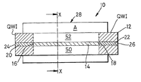
- FIG. 1 align a cross-sectional view of an optically active device according to a first embodiment of the present invention
- FIG. 2 a cross-sectional view through line X-X′ of the optically active device of FIG. 1;
- FIG. 3 a cross-sectional view of an optically active device according to a second embodiment of the present invention.
- FIGS. 1 and 2 there is illustrated an optically active device, generally designated 10 , according to a first embodiment of the present invention.
- the device 10 comprises a device body 12 , which in this embodiment is fabricated from a semiconductor material defining an optically active or optical gain region 14 which is bounded at first and second ends 16 , 18 thereof by optically passive regions 20 , 22 respectively.
- Outer ends 24 , 26 of the passive regions 20 , 22 define ends or facets 23 , 24 of the device 10 .
- a heatsink 28 is in thermal association with the device body 12 and arranged such that inner ends 16 , 18 of the passive regions 20 , 22 at ends 16 , 18 of the gain region 14 are provided within an area or extent “A” of the heatsink 28 , while the second ends 24 , 26 are provided outwith (outside) the area 28 , as viewed in the orientation of FIG. 1 .
- This arrangement provides passive regions 20 , 22 which “overhang” the heatsink 28 .
- Such an arrangement may be used for an optically active device 10 such as an optical amplifier, where access is required at both an input and output end of the.
- the passive regions 20 , 22 may be considered as input/output waveguides of the device 10 , which extend beyond opposite ends 24 , 26 of an optically active region of the device 10 .
- FIG. 2 shows the device 10 of FIG. 1 in cross-section along line X-X; as can be seen, the device 10 a is monolithic, being grown on a substrate 30 .
- the device body 12 is a layered structure comprising substrate 30 , upon which is grown by known techniques such as Molecular Beam Epitaxy (MBE)or Molecular Organic Chemical Vapour Deposition (MOCVD), a first optical cladding/charge carrier confining layer 36 , and active/guiding layer 32 , eg of semiconductor lasing material, and a second cladding/charge carrier confining layer 34 , and also beneficially semiconductor contact layer 40 .
- MBE Molecular Beam Epitaxy
- MOCVD Molecular Organic Chemical Vapour Deposition
- the device body 12 includes a waveguide 38 formed in the second cladding layer 34 by suitable etching techniques.
- the ridge 38 confines an optical beam within the optically active region 14 and the optically passive regions 20 , 22 (not shown).
- the ridge 38 extends between the ends 24 , 26 of the device 10 , 10 a.
- respective electrical contact layers 41 , 42 used to electrically drive the device 10 .
- the active layer 32 comprises a Quantum Well structure 54 embedded in the active layer 32 and, by confinement of the ridge 38 , the gain region 14 is located in the active layer 32 .
- the gain region 14 is laterally bounded by Quantum Well Intermixed (QWI) regions 50 , 52 which aid confinement of an optical beam within the Quantum Well structure of the gain region 14 .
- QWI Quantum Well Intermixed
- the passive regions 24 , 26 within the active layer 32 comprise Quantum Well Intermixed regions providing a higher band-gap energy and therefore lower absorption than the Quantum Well structure of the gain region 14 within the active layer 32 .
- This has an advantage that when the active region 14 is pumped with current heat dissipation at ends 16 , 18 of the active region 14 are provided with thermal contact to an area of heatsink 28 giving cooling of the device 10 , while the passive regions 20 , 22 overhang the heatsink 28 dissipating less heat.
- the ends 24 , 26 of the passive regions 20 , 22 are free from any obstruction of the heatsink 28 , thus giving clear access to the ends 24 , 26 of the device 10 for input/output coupling, eg to other optical devices.
- the device 10 is arranged in a “junction side-down” configuration so that the gain region 14 is as close to the heatsink 28 as possible. It will be appreciated that, in use, the heatsink 28 may be lowermost, and the (inverted) device body 12 uppermost.
- the distance between the heatsink 28 and the gain region 14 is likely to be typically around 2 to 5 ⁇ m.
- the heatsink 28 is chosen to be of a material having good thermal characteristics.
- the heatsink 28 is made substantially of Copper.
- other material such as Diamond, Silicon and Aluminium Nitride are appropriate also.
- the heatsink 28 is soldered or otherwise adhered to the contact 41 .
- the QW Intermixed regions are the passive regions 20 , 22 , in the active layer 32 shown in FIGS. 1 and 2.
- the ridge 38 is formed over the gain region 14 , and the passive regions 20 , 22 .
- an optically active device 10 made in a III-V semiconductor materials system such as GaAs or InP.
- the method begins with providing substrate layer 30 .
- the substrate is, in this embodiment Gallium Arsenide (GaAs) and is highly n-type doped.
- Grown on the substrate layer 30 is the first cladding layer 36 .
- the first cladding layer 36 comprises Aluminium Gallium Arsenide (AlGaAs) and is n-type doped to a first concentration.
- AlGaAs Aluminium Gallium Arsenide
- This first cladding layer 36 eg having a refractive of around 3.0 to 3.5, is typically 1 to 3 ⁇ m thick.
- Grown on the first cladding layer 36 is the semiconductor optically active layer 32 .
- the active layer 32 also comprises AlGaAs. Layer 32 is substantially intrinsic.
- the active layer 32 eg having a refractive index of around 3.0 to 3.5, is grown to be a few hundred nm thick, typically.
- a Quantum Well (QW) structure 54 Within the active layer 32 , is provided a Quantum Well (QW) structure 54 .
- the QW structure 54 is typically embedded in the middle of the layer 32 .
- the second cladding layer 34 is of p-type with a similar doping concentration to the first concentration.
- the second layer 34 is also made of AlGaAs with a thickness, composition, and refractive index similar to that of the first cladding layer 36 .
- QW Quantum Well
- Active layer 32 has a lower Aluminium (Al) content than cladding layers 34 , 36 .
- the active layer 32 has a higher refractive index than the cladding layers 36 , 34 .
- a selective QWI mask (not shown) is then placed at least over a portion of the device 10 where the ridge 38 will be defined, but leaving portions (coincident with the passive regions 20 , 22 to be formed) unmasked.
- the technique preferably used to create Quantum Well Intermixing (QWI) within the Quantum Well structure is a damage induced technique using vacancies.
- QWI Quantum Well Intermixing
- any other Quantum Well Intermixing technique which achieves a difference in the band-gap energy between the Quantum Well structure 54 and the QW intermixed passive regions 20 , 22 could be used within this invention.
- the damage induced technique requires depositing by use of a diode sputterer and within a substantially Argon atmosphere a dielectric layer such as Silica (SiO 2 ) on at least part of a surface of the semiconductor laser device material so as to introduce point structural defects at least into a portion of the material adjacent the dielectric layer;
- a dielectric layer such as Silica (SiO 2 )
- PECVD Plasma Enhanced Chemical Vapour Deposition
- portions of the second cladding layer 34 on either side of the ridge 38 is to be defined are etched away by known etching techniques once a suitable etch mask has been placed over an area defining the ridge 38 .
- a final layer 40 may be grown on the second cladding layer 34 , the final layer 40 being a highly doped p-type GaAs layer 40 .
- the final layer 40 acts as the upper contact for the device body 12 .
- Contact metallisation 41 , 42 are formed by known lithographic techniques on rib 38 , and on substrate 30 respectfully, so as to allow for electrical driving of the device body 12 . Finally the device body 12 is secured to the heatsink 28 .
- the device body 12 shown in the cross-section of FIG. 2 is a monolithic semiconductor active device.
- the active region 14 of the device 10 is within the active layer 32 and confined in the Quantum Well structure by the ridge 38 above.
- FIG. 3 there is shown an optically active device, generally designated 10 a, according to a second embodiment of the present invention.
- the device 10 a has similarities to the semiconductor device 10 of the first embodiment, and accordingly like parts have been given the same nomenclature but are suffixed “a”.
- the device 10 a comprises a device body 12 having an active region 14 a which is bounded on one end 18 a by an optically passive region 22 a , having a first end 25 a . Another end 16 a of the gain region 14 a and second end 26 a of the passive region 22 a define ends of the device 10 a .
- a heatsink 28 a is in thermal association with the device body 12 and arranged such that the ends 16 a , 18 a of the gain region 14 a are provided within an area A of the heatsink 28 a while the second end 26 a of the passive region 22 a is outwith (outside) the area A of the heatsink 28 a.
- This embodiment provides one passive region 22 a which “overhangs” the heatsink 28 a .
- Such an arrangement may be used for an optically active device such as a semiconductor laser diode where an output of the device 10 a is provided it is at end 26 a.
- the layered construction of the device 10 a is as described hereinbefore for the first embodiment with reference to FIGS. 1 and 2.
- the passive region 26 is a Quantum Well Intermixed (QWI) region providing a higher band-gap energy, and therefore lower absorption than the QW structure of the gain region 14 a.
- QWI Quantum Well Intermixed
- This arrangement has the advantage that the ends 16 a , 18 a of the gain region 14 a are provided in good thermal contact with the heatsink 28 a while clear access is given to the output end 26 a of the device 10 a , eg for output coupling to a fibre or other device.
- the device 10 a may be fabricated by a method similar to, or the same as, the method hereinbefore described for the device 10 .
- a principal advantage of the present invention is that, by the provision of passive regions at end(s) of an optical device overhanging a heatsink, problems associated with heating at facets of the device are improved as the regions are not active.
- a further advantage of the present invention is that coupling to the device is made easier by the protruding passive regions/waveguides which ensure the output/input beams are not impeded or influenced by the heatsink.
- a buried heterostructure waveguide could be used rather than a ridge waveguide.
- other waveguides such as Large Optical Cavity (LOC), Antiresonant Reflecting Optical Waveguide (ARROW), Wide Optical Waveguide (WOW), or the like could be used.
- LOC Large Optical Cavity
- ARROW Antiresonant Reflecting Optical Waveguide
- WOW Wide Optical Waveguide
Landscapes
- Physics & Mathematics (AREA)
- Condensed Matter Physics & Semiconductors (AREA)
- General Physics & Mathematics (AREA)
- Electromagnetism (AREA)
- Optics & Photonics (AREA)
- Semiconductor Lasers (AREA)
- Glass Compositions (AREA)
- Transition And Organic Metals Composition Catalysts For Addition Polymerization (AREA)
- Prostheses (AREA)
- Cold Air Circulating Systems And Constructional Details In Refrigerators (AREA)
Applications Claiming Priority (3)
| Application Number | Priority Date | Filing Date | Title |
|---|---|---|---|
| GB0101640 | 2001-01-23 | ||
| GB0101640.1 | 2001-01-23 | ||
| GB0101640A GB2371404B (en) | 2001-01-23 | 2001-01-23 | Improvements in or relating to optical devices |
Publications (2)
| Publication Number | Publication Date |
|---|---|
| US20020097763A1 US20020097763A1 (en) | 2002-07-25 |
| US6671300B2 true US6671300B2 (en) | 2003-12-30 |
Family
ID=9907274
Family Applications (1)
| Application Number | Title | Priority Date | Filing Date |
|---|---|---|---|
| US09/789,046 Expired - Lifetime US6671300B2 (en) | 2001-01-23 | 2001-02-20 | Optical devices |
Country Status (9)
| Country | Link |
|---|---|
| US (1) | US6671300B2 (zh) |
| EP (1) | EP1354381B1 (zh) |
| JP (1) | JP4027801B2 (zh) |
| CN (1) | CN1236534C (zh) |
| AT (1) | ATE298941T1 (zh) |
| DE (1) | DE60204848T2 (zh) |
| ES (1) | ES2246392T3 (zh) |
| GB (1) | GB2371404B (zh) |
| WO (1) | WO2002061898A1 (zh) |
Cited By (4)
| Publication number | Priority date | Publication date | Assignee | Title |
|---|---|---|---|---|
| US20070077017A1 (en) * | 2005-09-30 | 2007-04-05 | The Trustees Of Princeton University | Photonic integrated devices having reduced absorption loss |
| US20070217953A1 (en) * | 2006-03-16 | 2007-09-20 | Brennen Reid A | Optical detection cell with micro-fluidic chip |
| US20070218454A1 (en) * | 2006-03-16 | 2007-09-20 | Brennen Reid A | Optical detection cell for micro-fluidics |
| US7826693B2 (en) | 2006-10-26 | 2010-11-02 | The Trustees Of Princeton University | Monolithically integrated reconfigurable optical add-drop multiplexer |
Families Citing this family (4)
| Publication number | Priority date | Publication date | Assignee | Title |
|---|---|---|---|---|
| JP4697879B2 (ja) * | 2006-05-09 | 2011-06-08 | 東京エレクトロン株式会社 | サーバ装置、およびプログラム |
| US10203461B2 (en) * | 2015-09-04 | 2019-02-12 | Raytheon Company | Techniques for forming waveguides for use in laser systems or other systems and associated devices |
| WO2020204053A1 (ja) * | 2019-04-02 | 2020-10-08 | パナソニックセミコンダクターソリューションズ株式会社 | 半導体レーザ素子 |
| US11588302B2 (en) * | 2019-06-21 | 2023-02-21 | Seagate Technology Llc | Optical switches |
Citations (13)
| Publication number | Priority date | Publication date | Assignee | Title |
|---|---|---|---|---|
| US4282494A (en) | 1978-02-28 | 1981-08-04 | Nippon Electric Co., Ltd. | Stripe-geometry double heterojunction laser element |
| US4511408A (en) | 1982-04-22 | 1985-04-16 | The Board Of Trustees Of The University Of Illinois | Semiconductor device fabrication with disordering elements introduced into active region |
| US4585491A (en) | 1983-09-02 | 1986-04-29 | Xerox Corporation | Wavelength tuning of quantum well lasers by thermal annealing |
| US4594603A (en) | 1982-04-22 | 1986-06-10 | Board Of Trustees Of The University Of Illinois | Semiconductor device with disordered active region |
| US4639275A (en) | 1982-04-22 | 1987-01-27 | The Board Of Trustees Of The University Of Illinois | Forming disordered layer by controlled diffusion in heterojunction III-V semiconductor |
| US4727556A (en) | 1985-12-30 | 1988-02-23 | Xerox Corporation | Semiconductor lasers fabricated from impurity induced disordering |
| US4845216A (en) | 1985-03-08 | 1989-07-04 | The Trustees Of Princeton University | Pyrido [2,3,d]pyrimidine derivatives |
| US4845727A (en) | 1986-12-05 | 1989-07-04 | U. S. Philips Corporation | Divider circuit |
| US4857971A (en) | 1987-03-23 | 1989-08-15 | Xerox Corporation | (IV)x (III-V)1-x alloys formed in situ in III-V heterostructures |
| US4871690A (en) | 1986-01-21 | 1989-10-03 | Xerox Corporation | Semiconductor structures utilizing semiconductor support means selectively pretreated with migratory defects |
| US5327444A (en) * | 1989-04-20 | 1994-07-05 | Massachusetts Institute Of Technology | Solid state waveguide lasers |
| US5384797A (en) | 1992-09-21 | 1995-01-24 | Sdl, Inc. | Monolithic multi-wavelength laser diode array |
| US6326646B1 (en) * | 1999-11-24 | 2001-12-04 | Lucent Technologies, Inc. | Mounting technology for intersubband light emitters |
Family Cites Families (9)
| Publication number | Priority date | Publication date | Assignee | Title |
|---|---|---|---|---|
| JPS6054794B2 (ja) * | 1979-11-01 | 1985-12-02 | 富士通株式会社 | 光半導体装置 |
| DE3737191A1 (de) * | 1987-11-03 | 1989-05-24 | Fraunhofer Ges Forschung | Halbleiterdiodenlaser |
| DE3925201A1 (de) * | 1989-07-29 | 1991-02-07 | Messerschmitt Boelkow Blohm | Optische bank zur halterung optischer, elektrischer u.a. komponenten |
| JP2869279B2 (ja) * | 1992-09-16 | 1999-03-10 | 三菱電機株式会社 | 半導体レーザダイオード及びその製造方法並びに半導体レーザダイオードアレイ |
| JPH07162086A (ja) * | 1993-12-10 | 1995-06-23 | Mitsubishi Electric Corp | 半導体レーザの製造方法 |
| US5521406A (en) * | 1994-08-31 | 1996-05-28 | Texas Instruments Incorporated | Integrated circuit with improved thermal impedance |
| JPH08330672A (ja) * | 1995-05-31 | 1996-12-13 | Nec Corp | 半導体レーザ装置 |
| US5680412A (en) * | 1995-07-26 | 1997-10-21 | Demaria Electrooptics Systems, Inc. | Apparatus for improving the optical intensity induced damage limit of optical quality crystals |
| EP0757393A3 (en) * | 1995-08-02 | 1999-11-03 | Matsushita Electric Industrial Co., Ltd. | Semiconductor light emitting element and method for fabricating the same |
-
2001
- 2001-01-23 GB GB0101640A patent/GB2371404B/en not_active Revoked
- 2001-02-20 US US09/789,046 patent/US6671300B2/en not_active Expired - Lifetime
-
2002
- 2002-01-23 EP EP02716152A patent/EP1354381B1/en not_active Expired - Lifetime
- 2002-01-23 DE DE60204848T patent/DE60204848T2/de not_active Expired - Lifetime
- 2002-01-23 WO PCT/GB2002/000293 patent/WO2002061898A1/en active IP Right Grant
- 2002-01-23 JP JP2002561333A patent/JP4027801B2/ja not_active Expired - Fee Related
- 2002-01-23 CN CNB028040236A patent/CN1236534C/zh not_active Expired - Fee Related
- 2002-01-23 ES ES02716152T patent/ES2246392T3/es not_active Expired - Lifetime
- 2002-01-23 AT AT02716152T patent/ATE298941T1/de not_active IP Right Cessation
Patent Citations (13)
| Publication number | Priority date | Publication date | Assignee | Title |
|---|---|---|---|---|
| US4282494A (en) | 1978-02-28 | 1981-08-04 | Nippon Electric Co., Ltd. | Stripe-geometry double heterojunction laser element |
| US4511408A (en) | 1982-04-22 | 1985-04-16 | The Board Of Trustees Of The University Of Illinois | Semiconductor device fabrication with disordering elements introduced into active region |
| US4594603A (en) | 1982-04-22 | 1986-06-10 | Board Of Trustees Of The University Of Illinois | Semiconductor device with disordered active region |
| US4639275A (en) | 1982-04-22 | 1987-01-27 | The Board Of Trustees Of The University Of Illinois | Forming disordered layer by controlled diffusion in heterojunction III-V semiconductor |
| US4585491A (en) | 1983-09-02 | 1986-04-29 | Xerox Corporation | Wavelength tuning of quantum well lasers by thermal annealing |
| US4845216A (en) | 1985-03-08 | 1989-07-04 | The Trustees Of Princeton University | Pyrido [2,3,d]pyrimidine derivatives |
| US4727556A (en) | 1985-12-30 | 1988-02-23 | Xerox Corporation | Semiconductor lasers fabricated from impurity induced disordering |
| US4871690A (en) | 1986-01-21 | 1989-10-03 | Xerox Corporation | Semiconductor structures utilizing semiconductor support means selectively pretreated with migratory defects |
| US4845727A (en) | 1986-12-05 | 1989-07-04 | U. S. Philips Corporation | Divider circuit |
| US4857971A (en) | 1987-03-23 | 1989-08-15 | Xerox Corporation | (IV)x (III-V)1-x alloys formed in situ in III-V heterostructures |
| US5327444A (en) * | 1989-04-20 | 1994-07-05 | Massachusetts Institute Of Technology | Solid state waveguide lasers |
| US5384797A (en) | 1992-09-21 | 1995-01-24 | Sdl, Inc. | Monolithic multi-wavelength laser diode array |
| US6326646B1 (en) * | 1999-11-24 | 2001-12-04 | Lucent Technologies, Inc. | Mounting technology for intersubband light emitters |
Non-Patent Citations (24)
Cited By (6)
| Publication number | Priority date | Publication date | Assignee | Title |
|---|---|---|---|---|
| US20070077017A1 (en) * | 2005-09-30 | 2007-04-05 | The Trustees Of Princeton University | Photonic integrated devices having reduced absorption loss |
| US7333689B2 (en) * | 2005-09-30 | 2008-02-19 | The Trustees Of Princeton University | Photonic integrated devices having reduced absorption loss |
| US20070217953A1 (en) * | 2006-03-16 | 2007-09-20 | Brennen Reid A | Optical detection cell with micro-fluidic chip |
| US20070218454A1 (en) * | 2006-03-16 | 2007-09-20 | Brennen Reid A | Optical detection cell for micro-fluidics |
| US8647590B2 (en) | 2006-03-16 | 2014-02-11 | Agilent Technologies, Inc. | Optical detection cell with micro-fluidic chip |
| US7826693B2 (en) | 2006-10-26 | 2010-11-02 | The Trustees Of Princeton University | Monolithically integrated reconfigurable optical add-drop multiplexer |
Also Published As
| Publication number | Publication date |
|---|---|
| JP4027801B2 (ja) | 2007-12-26 |
| GB2371404A (en) | 2002-07-24 |
| ES2246392T3 (es) | 2006-02-16 |
| GB2371404B (en) | 2003-07-09 |
| EP1354381B1 (en) | 2005-06-29 |
| EP1354381A1 (en) | 2003-10-22 |
| US20020097763A1 (en) | 2002-07-25 |
| WO2002061898A1 (en) | 2002-08-08 |
| ATE298941T1 (de) | 2005-07-15 |
| GB0101640D0 (en) | 2001-03-07 |
| CN1236534C (zh) | 2006-01-11 |
| DE60204848D1 (de) | 2005-08-04 |
| JP2004523117A (ja) | 2004-07-29 |
| CN1488182A (zh) | 2004-04-07 |
| DE60204848T2 (de) | 2006-05-11 |
Similar Documents
| Publication | Publication Date | Title |
|---|---|---|
| US6717971B2 (en) | Semiconductor lasers | |
| US6674778B1 (en) | Electrically pumped edge-emitting photonic bandgap semiconductor laser | |
| US7656922B2 (en) | Multi-level integrated photonic devices | |
| US6717970B2 (en) | Lasers | |
| US6671300B2 (en) | Optical devices | |
| JP6247960B2 (ja) | 集積型半導体光素子、及び集積型半導体光素子の製造方法 | |
| US20020097942A1 (en) | Optical devices | |
| JP3061169B2 (ja) | 半導体レーザ | |
| US20040004217A1 (en) | Semiconductor opto-electronic devices with wafer bonded gratings | |
| JP3264321B2 (ja) | 導波路型半導体光集積素子およびその製造方法 | |
| CN1868099A (zh) | 具有结构化波导的面发射半导体激光器 | |
| Lammert et al. | Dual-channel strained-layer in GaAs-GaAs-AlGaAs WDM source with integrated coupler by selective-area MOCVD | |
| JPH10144990A (ja) | 導波路型光素子 | |
| JPH10290052A (ja) | 半導体レーザ装置 | |
| JP2022015036A (ja) | 半導体レーザ |
Legal Events
| Date | Code | Title | Description |
|---|---|---|---|
| AS | Assignment |
Owner name: UNIVERSITY COURT OF THE UNIVERSITY OF GLASGOW, THE Free format text: ASSIGNMENT OF ASSIGNORS INTEREST;ASSIGNORS:MARSH, JOHN HAIG;HAMILTON, CRAIG JAMES;REEL/FRAME:012101/0039;SIGNING DATES FROM 20010720 TO 20010723 |
|
| STCF | Information on status: patent grant |
Free format text: PATENTED CASE |
|
| CC | Certificate of correction | ||
| FPAY | Fee payment |
Year of fee payment: 4 |
|
| FPAY | Fee payment |
Year of fee payment: 8 |
|
| AS | Assignment |
Owner name: INTENSE INCORPORATED, NEW JERSEY Free format text: ASSIGNMENT OF ASSIGNORS INTEREST;ASSIGNOR:UNIVERSITY COURT OF THE UNIVERSITY OF GLASGOW, THE;REEL/FRAME:027588/0856 Effective date: 20110722 |
|
| FPAY | Fee payment |
Year of fee payment: 12 |