US6433393B1 - Semiconductor protective device and method for manufacturing same - Google Patents
Semiconductor protective device and method for manufacturing same Download PDFInfo
- Publication number
- US6433393B1 US6433393B1 US09/659,067 US65906700A US6433393B1 US 6433393 B1 US6433393 B1 US 6433393B1 US 65906700 A US65906700 A US 65906700A US 6433393 B1 US6433393 B1 US 6433393B1
- Authority
- US
- United States
- Prior art keywords
- well
- diffusion layer
- terminal
- type
- semiconductor
- Prior art date
- Legal status (The legal status is an assumption and is not a legal conclusion. Google has not performed a legal analysis and makes no representation as to the accuracy of the status listed.)
- Expired - Fee Related, expires
Links
- 230000001681 protective effect Effects 0.000 title claims abstract description 125
- 239000004065 semiconductor Substances 0.000 title claims abstract description 96
- 238000004519 manufacturing process Methods 0.000 title abstract description 21
- 238000000034 method Methods 0.000 title description 12
- 238000009792 diffusion process Methods 0.000 claims description 137
- 239000000758 substrate Substances 0.000 claims description 22
- 230000003068 static effect Effects 0.000 description 20
- 239000000463 material Substances 0.000 description 19
- 150000002500 ions Chemical class 0.000 description 15
- 230000015556 catabolic process Effects 0.000 description 9
- 229910052751 metal Inorganic materials 0.000 description 9
- 239000002184 metal Substances 0.000 description 9
- 238000000926 separation method Methods 0.000 description 6
- 230000005611 electricity Effects 0.000 description 5
- 230000003071 parasitic effect Effects 0.000 description 5
- 230000002829 reductive effect Effects 0.000 description 5
- 230000006378 damage Effects 0.000 description 4
- 238000004088 simulation Methods 0.000 description 4
- VYPSYNLAJGMNEJ-UHFFFAOYSA-N Silicium dioxide Chemical compound O=[Si]=O VYPSYNLAJGMNEJ-UHFFFAOYSA-N 0.000 description 2
- 230000007423 decrease Effects 0.000 description 2
- 238000010586 diagram Methods 0.000 description 2
- 239000012535 impurity Substances 0.000 description 2
- 230000002441 reversible effect Effects 0.000 description 2
- -1 BF2 ions Chemical class 0.000 description 1
- ZOXJGFHDIHLPTG-UHFFFAOYSA-N Boron Chemical compound [B] ZOXJGFHDIHLPTG-UHFFFAOYSA-N 0.000 description 1
- OAICVXFJPJFONN-UHFFFAOYSA-N Phosphorus Chemical compound [P] OAICVXFJPJFONN-UHFFFAOYSA-N 0.000 description 1
- XUIMIQQOPSSXEZ-UHFFFAOYSA-N Silicon Chemical compound [Si] XUIMIQQOPSSXEZ-UHFFFAOYSA-N 0.000 description 1
- 229910052785 arsenic Inorganic materials 0.000 description 1
- RQNWIZPPADIBDY-UHFFFAOYSA-N arsenic atom Chemical compound [As] RQNWIZPPADIBDY-UHFFFAOYSA-N 0.000 description 1
- 229910052796 boron Inorganic materials 0.000 description 1
- 230000003247 decreasing effect Effects 0.000 description 1
- 230000001419 dependent effect Effects 0.000 description 1
- 230000005669 field effect Effects 0.000 description 1
- 238000011835 investigation Methods 0.000 description 1
- 230000000670 limiting effect Effects 0.000 description 1
- 230000036961 partial effect Effects 0.000 description 1
- 229910052698 phosphorus Inorganic materials 0.000 description 1
- 239000011574 phosphorus Substances 0.000 description 1
- 229910021420 polycrystalline silicon Inorganic materials 0.000 description 1
- 229920005591 polysilicon Polymers 0.000 description 1
- 229910052710 silicon Inorganic materials 0.000 description 1
- 239000010703 silicon Substances 0.000 description 1
- 235000012239 silicon dioxide Nutrition 0.000 description 1
- 239000000377 silicon dioxide Substances 0.000 description 1
Images


Classifications
-
- H—ELECTRICITY
- H01—ELECTRIC ELEMENTS
- H01L—SEMICONDUCTOR DEVICES NOT COVERED BY CLASS H10
- H01L27/00—Devices consisting of a plurality of semiconductor or other solid-state components formed in or on a common substrate
- H01L27/02—Devices consisting of a plurality of semiconductor or other solid-state components formed in or on a common substrate including semiconductor components specially adapted for rectifying, oscillating, amplifying or switching and having at least one potential-jump barrier or surface barrier; including integrated passive circuit elements with at least one potential-jump barrier or surface barrier
- H01L27/04—Devices consisting of a plurality of semiconductor or other solid-state components formed in or on a common substrate including semiconductor components specially adapted for rectifying, oscillating, amplifying or switching and having at least one potential-jump barrier or surface barrier; including integrated passive circuit elements with at least one potential-jump barrier or surface barrier the substrate being a semiconductor body
-
- H—ELECTRICITY
- H01—ELECTRIC ELEMENTS
- H01L—SEMICONDUCTOR DEVICES NOT COVERED BY CLASS H10
- H01L27/00—Devices consisting of a plurality of semiconductor or other solid-state components formed in or on a common substrate
- H01L27/02—Devices consisting of a plurality of semiconductor or other solid-state components formed in or on a common substrate including semiconductor components specially adapted for rectifying, oscillating, amplifying or switching and having at least one potential-jump barrier or surface barrier; including integrated passive circuit elements with at least one potential-jump barrier or surface barrier
- H01L27/0203—Particular design considerations for integrated circuits
- H01L27/0248—Particular design considerations for integrated circuits for electrical or thermal protection, e.g. electrostatic discharge [ESD] protection
- H01L27/0251—Particular design considerations for integrated circuits for electrical or thermal protection, e.g. electrostatic discharge [ESD] protection for MOS devices
- H01L27/0259—Particular design considerations for integrated circuits for electrical or thermal protection, e.g. electrostatic discharge [ESD] protection for MOS devices using bipolar transistors as protective elements
- H01L27/0262—Particular design considerations for integrated circuits for electrical or thermal protection, e.g. electrostatic discharge [ESD] protection for MOS devices using bipolar transistors as protective elements including a PNP transistor and a NPN transistor, wherein each of said transistors has its base coupled to the collector of the other transistor, e.g. silicon controlled rectifier [SCR] devices
-
- H—ELECTRICITY
- H01—ELECTRIC ELEMENTS
- H01L—SEMICONDUCTOR DEVICES NOT COVERED BY CLASS H10
- H01L29/00—Semiconductor devices adapted for rectifying, amplifying, oscillating or switching, or capacitors or resistors with at least one potential-jump barrier or surface barrier, e.g. PN junction depletion layer or carrier concentration layer; Details of semiconductor bodies or of electrodes thereof ; Multistep manufacturing processes therefor
- H01L29/66—Types of semiconductor device ; Multistep manufacturing processes therefor
- H01L29/68—Types of semiconductor device ; Multistep manufacturing processes therefor controllable by only the electric current supplied, or only the electric potential applied, to an electrode which does not carry the current to be rectified, amplified or switched
- H01L29/70—Bipolar devices
- H01L29/74—Thyristor-type devices, e.g. having four-zone regenerative action
- H01L29/7436—Lateral thyristors
-
- H—ELECTRICITY
- H01—ELECTRIC ELEMENTS
- H01L—SEMICONDUCTOR DEVICES NOT COVERED BY CLASS H10
- H01L29/00—Semiconductor devices adapted for rectifying, amplifying, oscillating or switching, or capacitors or resistors with at least one potential-jump barrier or surface barrier, e.g. PN junction depletion layer or carrier concentration layer; Details of semiconductor bodies or of electrodes thereof ; Multistep manufacturing processes therefor
- H01L29/66—Types of semiconductor device ; Multistep manufacturing processes therefor
- H01L29/86—Types of semiconductor device ; Multistep manufacturing processes therefor controllable only by variation of the electric current supplied, or only the electric potential applied, to one or more of the electrodes carrying the current to be rectified, amplified, oscillated or switched
- H01L29/861—Diodes
- H01L29/87—Thyristor diodes, e.g. Shockley diodes, break-over diodes
-
- H—ELECTRICITY
- H01—ELECTRIC ELEMENTS
- H01L—SEMICONDUCTOR DEVICES NOT COVERED BY CLASS H10
- H01L2924/00—Indexing scheme for arrangements or methods for connecting or disconnecting semiconductor or solid-state bodies as covered by H01L24/00
- H01L2924/0001—Technical content checked by a classifier
- H01L2924/0002—Not covered by any one of groups H01L24/00, H01L24/00 and H01L2224/00
Definitions
- the present invention relates to a semiconductor protective device, and to a method of manufacturing a semiconductor protective device.
- an on-chip static electricity protective element in a semiconductor device comprising a fine-featured complimentary MOS semiconductor integrated circuit having a minimum interconnect width of 0.5 micron or less.
- the U.S. Pat. No. 5,502,317 has a disclosure of an N well 142 formed on the surface of a P-type semiconductor substrate 126 , a P-type diffusion layer 146 and N-type diffusion layer 144 connected to an external terminal formed therein, and N-type diffusion layer 114 formed on a semiconductor substrate 126 part of which is included in the N well 142 , an N-type diffusion layer 112 connected to a ground terminal 118 and an N-type diffusion layer 122 formed on the semiconductor substrate 126 , via an element separation region 124 .
- the PN junction formed by the N-type diffusion layer 114 and the P-type semiconductor substrate 126 exhibits an avalanche breakdown, thereby raising the potential on the substrate.
- the NPN transistor formed by the N-type diffusion layer 114 , the P-type semiconductor substrate 126 , and the N-type diffusion layer 112 conducts.
- the potential in the region of the P-type diffusion layer 146 of the N well 142 decreases, so that the PNP transistor formed by the P-type diffusion layer 146 , the N well 142 , and the P-type semiconductor substrate 126 conducts.
- the NPN transistor and PNP transistor operate in a complimentary manner so as to enhance the collector current, the result being entry into the low-resistance condition of so-called thyristor operation, thereby enabling protection of the internal circuit by causing a current to flow.
- FIG. 7 the basic configuration is the same as shown in FIG. 6, the major difference between FIG. 6 and FIG. 7 configurations being that, in place of the element separation region 124 shown in FIG. 6, in FIG. 7 a P-type diffusion layer 38 having a P-LDD structure is formed, the reverse withstand voltage of the PN junction at the boundary 40 between the P-type diffusion layer 38 and the N-type diffusion layer 20 being decreased, so that the trigger voltage for thyristor operation is lowered, thereby improving the protective capacity.
- This type of semiconductor protective element of the past is effective with respect to an external pulse having a slow rise time. However, it is poor in protective capacity with respect to a pulse having a fast rise time.
- CDM charged device model
- the element operates as a thyristor, but the starting speed is slow, so that a voltage greater than the breakdown voltage is applied to the internal circuit, thereby causing a low breakdown withstand voltage with respect to a fast pulse.
- the starting speed is dependent upon the distance Dac between the anode and the cathode electrodes of the thyristor element.
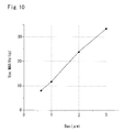
- FIG. 10 shows the results of a simulation for the case in which a thyristor element of the past is used as a protective element, with a CDM mode static electricity pulse of 1000 V applied, in which the relationship between the voltage VoxMAX applied to the internal circuitry to be protected and the distance Dac between the anode and cathode of the thyristor element is shown.
- FIG. 6 which shows the configuration of prior art as disclosed in the U.S. Pat. No. 5,502,317
- the reference numeral 146 denotes the anode electrode and 112 denotes the cathode electrode, there being an N-type diffusion layer 114 and element separation film 124 therebetween, which restricts the reduction of the anode-to-cathode distance Dac.
- FIG. 7 which shows the configuration of the specification of the U.S. Pat. No. 5,872,379 which discloses prior art
- the reference numeral 34 denotes the anode electrode and 18 denotes the cathode electrode, between which are interposed an N-type diffusion layer 20 and a P-type diffusion layer 38 , which make reduction of Dac difficult.
- the second case is that in which a negative CDM mode pulse is applied to a protective element of the past.
- the reason for a reduction in protective capacity in this case is that the element operates as a diode, wherein parasitic resistance of the element causes a rise in the voltage of the circuit to be protected.
- the inventors discovered by their simulations that the parasitic resistance is substantially proportional to the distance between the diode cathode and anode. It is therefore desirable to reduce the distance between the cathode and the anode of the diode, although this was difficult to achieve in the structure of the past.
- the N-type diffusion layer 20 acts as the cathode electrode and the P-type diffusion layer 14 acts as the anode electrode, with an N-type electrode 18 and a P-type electrode 38 interposed therebetween, so that there is a limitation on the reduction of the distance therebetween that can be achieved.
- the present invention has the following basic technical constitution.
- a first aspect of the present invention is a semiconductor protective device having a first well of a first conductive type, a second well of a second conductive type, being directly connected to said first well, a third well of a first conductive type being directly connected to one side of said second well which being opposite to the side thereof to which said first well being connected, each three wells being formed on a substrate, a first diffusion layer of a first conducive type formed within said second well of the second conductive type, a second diffusion layer of a second conducive type formed within said first well of said first conductive type and provided in proximal opposition to said first diffusion layer, a third diffusion layer of a second conductive type provided at a position over a boundary portion of said second well of a second conductive type and said third well of a first conductive type so as to bridge therebetween, said position being different from a position over a boundary portion of said second well of a second conductive type and said first well of a first conductive type where said first diffusion layer and said second diffusion layer being
- a second aspect of the present invention is a method for manufacturing a semiconductor protective device, this method having a step of disposing a first mask material on at least part of a semiconductor substrate and implanting a second conductivity ion therein to form a second well of a second conductivity type, a step of forming a second mask material minimally in a region in which said second well region is formed and implanting a first conductivity ion in a region that is directly in contact with said second well region but outside said second well region, so as to form a first well of first conductivity type and a third well of a first conductivity type, a step of forming a third mask material having a first aperture formed at a position opposite a region that minimally bridges said third well region and said second well region and a second aperture formed at a position in said first well region and nearly opposite to said second well of said second conductivity type region, and implanting a second conductivity ion, so as to form a third and a second diffusion layers of said second conductivity, respectively,
- a semiconductor protective device and method for manufacturing a semiconductor protective device according to the present invention provide a thyristor element having the first diffusion layer as an anode and the second diffusion layer as a cathode, which operates in this manner when a positive overvoltage pulse is applied.
- this distance can be established as 1 ⁇ m or smaller.
- the operation is as a diode having the third diffusion layer as a cathode and the fourth diffusion layer as an anode.
- the operation is as a diode having the third diffusion layer as a cathode and the fourth diffusion layer as an anode.
- FIG. 1 is a drawing showing the general configuration of an example of a semiconductor protective device according to the present invention.
- FIG. 1 ⁇ A) showing a plan view thereof
- FIG. 1 (B) showing a cross-sectional view thereof, along the line a-a′ of FIG. 1 (A).
- FIG. 2 is a block diagram showing an example of an input circuit in which a semiconductor protective device according to the present invention has been built in as a main protective element.
- FIG. 3 is a block diagram showing an example of an input circuit in which a semiconductor protective device according to the present invention is built in as an auxiliary protective element.
- FIG. 4 is a cross-sectional view illustrating an example of the constitution of a method for manufacturing a semiconductor protective device according to the present invention.
- FIG. 5 is a cross-sectional view illustrating an example of the constitution of a method for manufacturing a semiconductor protective device according to the present invention.
- FIG. 6 is a cross-sectional view showing an example of the configuration of a semiconductor protective device of the past.
- FIG. 7 is a cross-sectional view showing an example of the configuration of a semiconductor protective device of the past.
- FIG. 8 is a drawing illustrating operation of a part of a semiconductor protective device according to the present invention.
- FIG. 9 is a drawing illustrating operation of a part of a semiconductor protective device according to the present invention.
- FIG. 10 is a graph that shows the relationship between the anode-to-cathode distance of a protective element when a 1000-volt CDM mode static pulse is applied to the input circuit, into which the semiconductor protective device of the present invention is built, as a main protection element, with the maximum voltage VoxMAX applied to the internal circuit.
- FIG. 1 (A) is a plan view showing a specific configuration of a semiconductor protective device according to the present invention
- FIG. 1 (B) is a cross-sectional view thereof.
- These drawings show a semiconductor protective device 300 having a first well of a first conductive type 101 , a second well of a second conductive type 102 , being directly connected to said first well 101 , a third well of a first conductive type 101 ′ being directly connected to one side of said second well 102 which being opposite to the side thereof to which said first well 101 being connected, each three wells being formed on a substrate 100 , a first diffusion layer of a first conducive type 103 formed within said second well of the second conductive type 102 , a second diffusion layer of a second conducive type 104 formed within said first well of said first conductive type 101 and provided in proximal opposition to said first diffusion layer 103 , a third diffusion layer of a second conductive type 105 provided at a position over a boundary portion 203 of said second well of
- FIG. 1 (A) the second well 102 is surrounded by the first well 101 but FIG. 1 (B) shows that the second well 102 is sandwiched with the first well 101 and thus in order to easy explanation about this configuration of the present invention, the left hand side first well portion is referred to a third well region 101 ′ although the third well region 101 ′ and the first well region 101 are integrally formed.
- the reference numeral 110 denotes a terminal interconnect that is connected to a metal interconnect formed as the first terminal 107
- the reference numeral 111 denotes a contact hole
- FIG. 1 (B) is a cross-sectional view seen along the line a-a′ of FIG. 1 (A).
- FIG. 1 shows a specific example of a semiconductor protective device 300 according to the present invention as shown in FIG. 1, in which the second conductivity well 102 is formed as an island within the well 101 of the first conductivity, the first and second diffusion layers 103 and 104 being disposed in proximity and so as to surround the boundary 201 between the first conductivity well 101 and second conductivity well 102 , and the third diffusion layer 105 being disposed within both wells so as to bridge the boundary edge 203 between the third conductivity well 101 ′ and the second conductivity well 102 which is located in opposition to the boundary edge 201 formed between the first conductivity well 101 and the second conductivity well 102 .
- the fourth diffusion layer 106 is shown as formed within the third conductivity well 101 ′ in proximity to and parallel to the third diffusion layer 105 .
- the first to fourth diffusion layers it is not necessary to have the first to fourth diffusion layers disposed in series.
- the third and fourth diffusion layer 105 and 106 or the like disposed at a position 202 or 204 forming the boundary between the first conductivity well 101 and the second conductivity well 102 .
- the first terminal 107 and the terminal interconnect 110 connected thereto are the input terminals of the semiconductor device requiring protection, and the second terminal 108 is desirably made a ground terminal.
- the semiconductor circuit to be protected by the present invention be constituted of MOS semiconductor elements, specifically the MOS integrated circuit to be protected by the present invention can include an inverter circuit formed by at least one P-type MOS transistor and one N-type MOS transistor, the gate of which is an input/output signal terminal, and the source of the N-type MOS transistor of which is a ground terminal, thereby forming a CMOS inverter.
- the semiconductor protective device 300 of the present invention is formed mainly by MOS transistors, so that it is desirable that the semiconductor device to be protected thereby, for example, is a device formed by MOS semiconductor elements, thereby enabling use of common manufacturing processes, so as to improve efficiency and reduce costs.
- the semiconductor protective device 300 of the present invention it is necessary to form a thyristor structure by the first diffusion layer 103 , the second conductivity well 102 , the first conductivity well 101 , and the second diffusion layer 104 , and also necessary to form a diode between the third diffusion layer 105 and the fourth diffusion layer 106 .
- the straight-line distance Y (i.e., Dac) between the first diffusion layer 103 and the second diffusion layer 104 forming the thyristor structure must be formed so as to be as short as possible, and this is desirably made 2 ⁇ m or less and further desirably made 1 ⁇ m or less.
- the distance X between the third diffusion layer 105 and the fourth diffusion layer 106 in the diode formed between the third diffusion layer 105 and the fourth diffusion layer 106 be as short as possible.
- the structure of the third diffusion layer 105 in the present invention is desirably formed so that the major portion thereof 250 is disposed within the second conductivity well 102 , and so that the other part 251 of the third diffusion layer 105 is disposed within the third conductivity well 101 ′.
- a contact 107 be connected to the surface at a position on the third diffusion layer 105 disposed within the second conductivity well 102 .
- a diode formed between the third diffusion layer 105 and the the third well region of the first conductivity type 101 ′ operate as a trigger that drives the thyristor structure.
- the semiconductor protective device 300 of the present invention adopts the basic constitution described above, in the case of a positive overvoltage, operation is as a thyristor elements, with the first diffusion layer 103 acting as an anode, and the second diffusion layer 104 acting as a cathode.
- the distance Dac between the anode and the cathode can be reduced to within the allowable limits of LSI manufacturing technology, and this distance can be made 1 ⁇ m or less for the case of a CMOS LSI device having a 0.25 ⁇ m design rule.
- the operation is as a diode having the third diffusion layer 105 acting as a cathode and the fourth diffusion layer 106 acting as an anode.
- the distance between the cathode and the anode within the allowable limits of manufacturing technology, thereby enabling the achievement of a diode with an extremely low internal resistance. For this reason, even in the case of a large discharge current value, it is possible to limit the voltage rise in the internal circuit.
- the operation of the semiconductor protective device 300 is as a PNPN thyristor element formed by a P-type diffusion layer 103 , and N-type well 102 , a P-type well 101 , and an N-type diffusion layer 104 , so that the internal resistance is greatly reduced.
- the distance Dac between the anode electrode (P-type diffusion layer 103 ) and the cathode electrode (N-type diffusion layer 104 ) is 1 ⁇ m or smaller, the starting speed of the semiconductor protective circuit 300 is high, so that in accordance with FIG. 10, even if a CDM mode pulse of 1000 V is applied, the voltage rise in the internal circuit is limited to less than 15 volts. Advances in manufacturing technology enable Dac to be made very small.
- the semiconductor protective circuit 300 operates as a diode having the N-type diffusion layer 105 acting as a cathode electrode and the P-type diffusion layer 106 acting as an anode electrode.
- the internal resistance during operation does not exceed 1 ohm. Therefore, even if the discharge current maximum value is 10 A, the voltage across the terminals of the protective element does not exceed 10 V.
- the semiconductor protective device 300 upon investigating the cause for the effective operation of the thyristor structure, it was verified that, because of the phenomenon describe below, the above-noted thyristor structure is driven at a high speed.
- this current is the base current of an NPN bipolar transistor formed by the N-type well 102 , the P-type well 101 , and the N-type diffusion layer 104 , thereby resulting in conduction of this NPN bipolar transistor, which results in a flow of current from the N-type diffusion layer 105 which is the collector electrode into the N-type diffusion layer 104 which is the emitter electrode.
- the current is the base current of a PNP bipolar transistor formed by the P-type diffusion layer 103 , the N-type well 102 , and the P-type well 101 , so that the PNP transistor conducts, the result being, as shown in FIG. 9 ( c ), that the collector current flows from the P-type diffusion layer 103 to the P-type well 101 .
- the collector current of the above noted NPN transistor and PNP transistor are the base currents of the opposing transistor, so that they act to strengthen the collector current. Essentially, this forms a PNPN thyristor action, so that before the voltage on the internal circuit rises and the overvoltage pulse reaches a peak, a large amount of current flows through the low internal resistance thereby protecting the internal circuit.
- a diode formed between the third diffusion layer 105 and first conductivity well 101 or between the third diffusion layer 105 and the fourth diffusion layer 106 acts as a trigger for the thyristor structure.
- FIG. 2 shows an example in which a protective element 300 of the present invention, shown in FIG. 1, is built into the input circuit of an integrated circuit.
- FIG. 2 there is an internal circuit 302 connected via a resistance R 1 which has a terminal 210 as an external connection terminal, and a semiconductor protection device 301 of the present invention, having an element width W of 50 ⁇ m is interposed between this external terminal 210 and the ground interconnect.
- a MOS-type integrated circuit 302 to be protected that has at least one ground terminal and one input/output signal terminal, and which is formed on a semiconductor substrate, is connected to an external terminal via a first resistance connected to the input/output signal terminal provided on the substrate, the semiconductor protective device 301 according to the present invention being connected to the second terminal of the external terminal 210 .
- the protective element 302 goes into the conducting condition, as described above, so that current flows, thereby clamping the voltage across the terminals.
- the resistance R 1 prevents a rise in the voltage of the internal circuits before the protective element starts to conduct, at the initial 200 ps of the overvoltage.
- the value of R 1 should be in a range from 50 ohm to 200 ohm.
- FIG. 3 shows another example, in which the protective element 300 of the present invention is built in as an auxiliary protective element of the input circuit of an integrated circuit.
- the element 210 is an external connection terminal, there being an internal circuit 302 connected thereto via the series connection of resistances R 1 and R 2 , an N-type MOS FET 303 having a grounded gate being connected between the terminal 210 and the ground interconnect 304 as a main protective element.
- the protective element 301 of the present invention is built in between the junction point between the resistances R 1 and R 2 and the ground interconnect connection point.
- a protective element has a width W of 10 ⁇ m.
- a semiconductor protective device 300 has a MOS-type integrated circuit to be protected with at least one ground terminal and one input/output signal terminal, formed on a semiconductor substrate, an external terminal formed on the semiconductor substrate, a first and a second resistor connected in series with one another, a first protective element, and a ground interconnect formed by a metal.
- the first resistor is connected to the junction between the external terminal and the second resistor, and the second resistor is connected between this junction point and at least one of the input/output signal terminals, the first protective element being connected between the external terminal and one end of the metal ground interconnect, and another end of the metal ground interconnect being connected to at least one ground terminal of the MOS-type integrated circuit.
- the first terminal of a semiconductor protective device 300 configured in this manner is connected to the external terminal, and the second terminal is connected to the ground terminal, the first terminal being connected to the contact point 1 and the second terminal of the second semiconductor protective device being minimally connected to one of the ground terminals of the MOS-type integrated circuit.
- the N-type MOS transistor of the main protective element operates as a parasitic bipolar device, so that discharge current flows from the main protective element to the ground point, via the ground interconnect 304 .
- the parasitic resistance Rg of the ground interconnect a high voltage occurs between the external terminal 310 and the ground point.
- a protective element of the present invention is introduced as the auxiliary protective element 301 , the auxiliary protective element is started at a high speed, based on the same principle as described earlier, and the internal resistance is greatly reduced, so that the voltage applied to the internal circuit is limited.
- an HBM mode pulse is applied which would cause thermal destruction, because of the resistance R 1 , there is almost no current flowing in the main protective element 303 .
- the width of the main protective element By making the width of the main protective element large, it is possible to prevent destruction of the main protective element itself. Because an HBM mode static pulse does not reach the auxiliary protective element, even if the width of the element in the auxiliary protective element is reduce to 10 ⁇ m, there is no destruction of the auxiliary element itself, and the reduction of the size reduces the amount of surface area occupied by the auxiliary protective element on the chip.
- the value of the resistance R 2 is such that it prevents a rise in voltage applied to the internal circuit during the initial 200 ps before the auxiliary protective element begins to operate.
- the resistance R 1 is made 50 ohm and the resistance R 2 is made 50 ohm.
- a first aspect of the method for manufacturing a semiconductor protective device in the present invention is such that which comprising, a step of disposing a first mask material on at least part of a semiconductor substrate and implanting a second conductivity ion therein to form a second well of a second conductivity type, a step of forming a second mask material minimally in a region in which said second well region is formed and implanting a first conductivity ion in a region that is directly in contact with said second well region but outside said second well region, so as to form a first well of first conductivity type and a third well of a first conductivity type, a step of forming a third mask material having a first aperture formed at a position opposite a region that minimally bridges said third well region and said second well region and a second aperture formed at a position in said first well region and nearly opposite to said second well of said second conductivity type region, and implanting a second conductivity ion, so as to form a third and a second diffusion layers of said second conductivity,
- a second aspect of the method for manufacturing a semiconductor protective device in the present invention is such that which comprising, a step of disposing an island-shaped first mask material on at least part of a semiconductor substrate and implanting a second conductivity ion therein to form an island-shaped second well region of a second conductivity type, a step of disposing a second mask material minimally in a region in which said second well region is formed and implanting a first conductive ion in a region outside said second well region, so as to form a first well region and a third well region of a first conductive type, a step of forming a third mask material having a first aperture formed at a position corresponding to a region that minimally bridges said third well region and said second well region and a second aperture formed at a position in said first well region and oppositely close to said second well region and implanting a second conductive ion into said second well region, so as to form a third diffusion layer and a second diffusion layer, respectively, and a step of forming
- a mask material 410 is formed onto a silicon semiconductor substrate 400 and boron (B) ions are implanted therein, to form a P-type well 401 (corresponding to the first well 101 and the third well 101 ′) having a depth of approximately 2 ⁇ m, with an impurity concentration of approximately 5 ⁇ 10 17 /cm 3 .
- a mask material 420 is formed and phosphorus (P) ions are implanted therein, to form an N-type well 402 having a thickness of approximately 2 ⁇ m and an impurity concentration of approximately 5 ⁇ 10 17 /cm 3 , after which the mask material is removed, as shown in FIG. 4 (C), to form a silicon dioxide film element separation 405 having a depth of approximately 400 nm in the form of a trench, a gate oxide film 406 having a thickness of approximately 8 nm being formed, after which a gate electrode 407 is formed using a polysilicon film.
- a mask material 430 is formed, and arsenic (As) ions are implanted therein to form the N-type diffusion layers 403 - 1 , 403 - 2 , and 402 - 3 , and 403 - 4 , which are self-aligned with respect to the element separation film and the gate electrode.
- As arsenic
- the concentration of the N-type diffusion layers is approximately 2 ⁇ 10 20 /cm 3 and the thickness thereof is approximately 300 nm.
- a mask material 440 is formed so as to cover part of the N-type diffusion layer, after which BF 2 ions are implanted therein to form the P-type diffusion layers 404 - 1 , 404 - 2 , 404 - 3 , and 404 - 4 , which are self-aligned with respect to the element separation film and the gate electrode.
- the concentration in the P-type diffusion layers is approximately 1 ⁇ 10 2 /cm 3 , and the thickness thereof is approximately 300 nm.
- the mask material is removed, and as shown in FIG. 5 (F), interconnect contacts 408 - 1 , 408 - 2 , 408 - 3 , 408 - 4 , and 408 - 5 are formed on each of the N-type and P-type diffusion layers.
- the diffusion layer 404 - 1 corresponds to the first diffusion layer of the protective element of the present invention
- the diffusion layer 403 - 1 corresponds to the second diffusion layer thereof
- the diffusion layer 403 - 2 corresponds to the third diffusion layer thereof
- the diffusion layer 404 - 2 corresponds to the fourth diffusion layer thereof.
- the diffusion layers 403 - 3 and 403 - 4 correspond to the drain and source diffusion layers of an N-type MOS transistor forming the internal circuit
- the diffusion layers 404 - 3 and 404 - 4 correspond to the drain and the source of the P-type MOS transistor forming the internal circuit.
- the metal interconnect 408 - 1 is connected to the external terminal, the metal interconnect 408 - 2 is connected to the ground interconnect, the metal interconnect 408 - 3 is connected, for example, to a ground interconnect, the metal interconnect 408 - 4 is connected to another connection point on the internal circuit, and the metal interconnect 408 - 5 is connected, for example, to a power supply terminal.
- a semiconductor circuit using a protective element according to the present invention prevents breakdown of the internal circuit even in the case of a high-speed pulse such as a CDM mode pulse, thereby enabling a high static electric withstand voltage.
- the reason for this is that it is possible to make the distance between the anode and the cathode when the protective element operates as a thyristor and the distance between the anode and the cathode when the device operates as a diode minimum, and by doing so it is possible to achieve a fast element startup, thereby reducing the internal resistance.
- the distance between the anode and the cathode can be further reduced, thereby preventing a reduction in withstand voltage that accompanies a reduction of feature size in device elements.
Applications Claiming Priority (2)
| Application Number | Priority Date | Filing Date | Title |
|---|---|---|---|
| JP25582999A JP3317285B2 (ja) | 1999-09-09 | 1999-09-09 | 半導体保護装置とこれを含む半導体装置及びそれらの製造方法 |
| JP11-255829 | 1999-09-09 |
Publications (1)
| Publication Number | Publication Date |
|---|---|
| US6433393B1 true US6433393B1 (en) | 2002-08-13 |
Family
ID=17284194
Family Applications (1)
| Application Number | Title | Priority Date | Filing Date |
|---|---|---|---|
| US09/659,067 Expired - Fee Related US6433393B1 (en) | 1999-09-09 | 2000-09-11 | Semiconductor protective device and method for manufacturing same |
Country Status (4)
| Country | Link |
|---|---|
| US (1) | US6433393B1 (ja) |
| JP (1) | JP3317285B2 (ja) |
| KR (1) | KR100344706B1 (ja) |
| CN (1) | CN1197155C (ja) |
Cited By (4)
| Publication number | Priority date | Publication date | Assignee | Title |
|---|---|---|---|---|
| US20030179523A1 (en) * | 2002-03-25 | 2003-09-25 | Nec Electronics Corporation | Electrostatic discharge protection device |
| US8414962B2 (en) | 2005-10-28 | 2013-04-09 | The Penn State Research Foundation | Microcontact printed thin film capacitors |
| US9558806B1 (en) * | 2015-07-28 | 2017-01-31 | Renesas Electronics Corporation | Electronic device |
| CN117038720A (zh) * | 2023-10-07 | 2023-11-10 | 江苏应能微电子股份有限公司 | 双齐纳阱scr器件、制造工艺及其堆叠结构 |
Families Citing this family (3)
| Publication number | Priority date | Publication date | Assignee | Title |
|---|---|---|---|---|
| JP3810375B2 (ja) | 2003-03-14 | 2006-08-16 | ローム株式会社 | 半導体装置 |
| US7106568B2 (en) * | 2004-08-27 | 2006-09-12 | United Microelectronics Corp. | Substrate-triggered ESD circuit by using triple-well |
| JP5820311B2 (ja) * | 2012-03-02 | 2015-11-24 | ルネサスエレクトロニクス株式会社 | 半導体装置 |
Citations (11)
| Publication number | Priority date | Publication date | Assignee | Title |
|---|---|---|---|---|
| JPS59181044A (ja) | 1983-03-31 | 1984-10-15 | Toshiba Corp | 入力保護回路 |
| JPS62165966A (ja) | 1986-01-17 | 1987-07-22 | Sanyo Electric Co Ltd | 半導体装置 |
| US5502317A (en) | 1993-07-14 | 1996-03-26 | Texas Instruments Incorporated | Silicon controlled rectifier and method for forming the same |
| JPH09191082A (ja) | 1995-09-29 | 1997-07-22 | Texas Instr Inc <Ti> | 高速バイポーラ/BiCMOS回路のESD保護のための改良されたバイポーラSCRトリガリング |
| JPH09223748A (ja) | 1995-12-14 | 1997-08-26 | Nec Corp | 半導体装置 |
| US5872379A (en) | 1997-07-10 | 1999-02-16 | Taiwan Semiconductor Manufacturing Co. Ltd. | Low voltage turn-on SCR for ESD protection |
| US5994741A (en) * | 1992-09-25 | 1999-11-30 | Kabushiki Kaisha Toshiba | Semiconductor device having digital and analog circuits integrated on one chip |
| US6281527B1 (en) * | 1998-02-12 | 2001-08-28 | Winbond Electronics Corp. | Electrostatic discharge protection circuit with high trigger current |
| US6355959B1 (en) * | 2000-09-11 | 2002-03-12 | National Semiconductor Corporation | Gate electrode controllable electrostatic discharge (ESD) protection structure having a MOSFET with source and drain regions in separate wells |
| US6355960B1 (en) * | 2000-09-18 | 2002-03-12 | Vanguard International Semiconductor Corporation | ESD protection for open drain I/O pad in integrated circuit with parasitic field FET devices |
| US6359313B1 (en) * | 1998-05-18 | 2002-03-19 | Samsung Electronics Co., Ltd. | Electrostatic discharge protection transistor for a semiconductor chip |
-
1999
- 1999-09-09 JP JP25582999A patent/JP3317285B2/ja not_active Expired - Fee Related
-
2000
- 2000-09-06 KR KR1020000052808A patent/KR100344706B1/ko not_active IP Right Cessation
- 2000-09-08 CN CNB001243551A patent/CN1197155C/zh not_active Expired - Fee Related
- 2000-09-11 US US09/659,067 patent/US6433393B1/en not_active Expired - Fee Related
Patent Citations (11)
| Publication number | Priority date | Publication date | Assignee | Title |
|---|---|---|---|---|
| JPS59181044A (ja) | 1983-03-31 | 1984-10-15 | Toshiba Corp | 入力保護回路 |
| JPS62165966A (ja) | 1986-01-17 | 1987-07-22 | Sanyo Electric Co Ltd | 半導体装置 |
| US5994741A (en) * | 1992-09-25 | 1999-11-30 | Kabushiki Kaisha Toshiba | Semiconductor device having digital and analog circuits integrated on one chip |
| US5502317A (en) | 1993-07-14 | 1996-03-26 | Texas Instruments Incorporated | Silicon controlled rectifier and method for forming the same |
| JPH09191082A (ja) | 1995-09-29 | 1997-07-22 | Texas Instr Inc <Ti> | 高速バイポーラ/BiCMOS回路のESD保護のための改良されたバイポーラSCRトリガリング |
| JPH09223748A (ja) | 1995-12-14 | 1997-08-26 | Nec Corp | 半導体装置 |
| US5872379A (en) | 1997-07-10 | 1999-02-16 | Taiwan Semiconductor Manufacturing Co. Ltd. | Low voltage turn-on SCR for ESD protection |
| US6281527B1 (en) * | 1998-02-12 | 2001-08-28 | Winbond Electronics Corp. | Electrostatic discharge protection circuit with high trigger current |
| US6359313B1 (en) * | 1998-05-18 | 2002-03-19 | Samsung Electronics Co., Ltd. | Electrostatic discharge protection transistor for a semiconductor chip |
| US6355959B1 (en) * | 2000-09-11 | 2002-03-12 | National Semiconductor Corporation | Gate electrode controllable electrostatic discharge (ESD) protection structure having a MOSFET with source and drain regions in separate wells |
| US6355960B1 (en) * | 2000-09-18 | 2002-03-12 | Vanguard International Semiconductor Corporation | ESD protection for open drain I/O pad in integrated circuit with parasitic field FET devices |
Non-Patent Citations (1)
| Title |
|---|
| US 6,351, 012, 02/2002, Hirata (withdrawn) * |
Cited By (7)
| Publication number | Priority date | Publication date | Assignee | Title |
|---|---|---|---|---|
| US20030179523A1 (en) * | 2002-03-25 | 2003-09-25 | Nec Electronics Corporation | Electrostatic discharge protection device |
| US7109533B2 (en) | 2002-03-25 | 2006-09-19 | Nec Electronics Corporation | Electrostatic discharge protection device |
| US8414962B2 (en) | 2005-10-28 | 2013-04-09 | The Penn State Research Foundation | Microcontact printed thin film capacitors |
| US8828480B2 (en) | 2005-10-28 | 2014-09-09 | The Penn State Research Foundation | Microcontact printed thin film capacitors |
| US9558806B1 (en) * | 2015-07-28 | 2017-01-31 | Renesas Electronics Corporation | Electronic device |
| CN117038720A (zh) * | 2023-10-07 | 2023-11-10 | 江苏应能微电子股份有限公司 | 双齐纳阱scr器件、制造工艺及其堆叠结构 |
| CN117038720B (zh) * | 2023-10-07 | 2024-01-26 | 江苏应能微电子股份有限公司 | 双齐纳阱scr器件、制造工艺及其堆叠结构 |
Also Published As
| Publication number | Publication date |
|---|---|
| KR100344706B1 (ko) | 2002-07-20 |
| JP3317285B2 (ja) | 2002-08-26 |
| KR20010030290A (ko) | 2001-04-16 |
| CN1288263A (zh) | 2001-03-21 |
| JP2001085534A (ja) | 2001-03-30 |
| CN1197155C (zh) | 2005-04-13 |
Similar Documents
| Publication | Publication Date | Title |
|---|---|---|
| US4987465A (en) | Electro-static discharge protection device for CMOS integrated circuit inputs | |
| US5717559A (en) | Input/output protection device for use in semiconductor device | |
| JP3911566B2 (ja) | Mos型半導体装置 | |
| KR0139648B1 (ko) | 트리거 전압이 낮은 scr 보호장치 및 보호회로 | |
| KR100282760B1 (ko) | 정전기적 방전 방지용 회로 및 구조 | |
| US7986011B2 (en) | Electrostatic discharge protection device | |
| JP3573674B2 (ja) | 半導体集積回路の入出力保護装置とその保護方法 | |
| US6479872B1 (en) | Dynamic substrate-coupled electrostatic discharging protection circuit | |
| KR0159451B1 (ko) | 반도체장치의 보호회로 | |
| JPH06196634A (ja) | 空乏制御型分離ステージ | |
| US5814865A (en) | Bimodal ESD protection for DRAM power supplies and SCRs for DRAMs and logic circuits | |
| US20040042143A1 (en) | Electrostatic discharge protection circuit with active device | |
| JPH0864812A (ja) | 過電圧保護半導体スイッチ | |
| US5710452A (en) | Semiconductor device having electrostatic breakdown protection circuit | |
| US6433393B1 (en) | Semiconductor protective device and method for manufacturing same | |
| EP0472654B1 (en) | Low voltage triggered snap-back device | |
| JP3317345B2 (ja) | 半導体装置 | |
| JP3559075B2 (ja) | Cmos技術の集積電子回路用の極性反転保護装置 | |
| EP0772237B1 (en) | Semiconductor device including protection means | |
| JPH05505060A (ja) | 低トリガ電圧scr保護装置及び構造 | |
| KR100435807B1 (ko) | 정전방전 보호 회로용 반도체 제어 정류기 | |
| JPH07263633A (ja) | 半導体装置の対静電気放電保護装置 | |
| JP3033739B2 (ja) | 静電気保護回路 | |
| JPH0715010A (ja) | 半導体装置の保護回路 | |
| JP2500802B2 (ja) | 半導体装置 |
Legal Events
| Date | Code | Title | Description |
|---|---|---|---|
| AS | Assignment |
Owner name: NEC CORPORATION, JAPAN Free format text: ASSIGNMENT OF ASSIGNORS INTEREST;ASSIGNOR:NARITA, KAORU;REEL/FRAME:011093/0887 Effective date: 20000802 |
|
| FEPP | Fee payment procedure |
Free format text: PAYOR NUMBER ASSIGNED (ORIGINAL EVENT CODE: ASPN); ENTITY STATUS OF PATENT OWNER: LARGE ENTITY |
|
| FPAY | Fee payment |
Year of fee payment: 4 |
|
| FPAY | Fee payment |
Year of fee payment: 8 |
|
| REMI | Maintenance fee reminder mailed | ||
| LAPS | Lapse for failure to pay maintenance fees | ||
| STCH | Information on status: patent discontinuation |
Free format text: PATENT EXPIRED DUE TO NONPAYMENT OF MAINTENANCE FEES UNDER 37 CFR 1.362 |
|
| FP | Lapsed due to failure to pay maintenance fee |
Effective date: 20140813 |