US5339167A - Reproduction speed controller for image signal reproducing apparatus - Google Patents
Reproduction speed controller for image signal reproducing apparatus Download PDFInfo
- Publication number
- US5339167A US5339167A US07/992,529 US99252992A US5339167A US 5339167 A US5339167 A US 5339167A US 99252992 A US99252992 A US 99252992A US 5339167 A US5339167 A US 5339167A
- Authority
- US
- United States
- Prior art keywords
- field image
- signal
- read
- reference signal
- write
- Prior art date
- Legal status (The legal status is an assumption and is not a legal conclusion. Google has not performed a legal analysis and makes no representation as to the accuracy of the status listed.)
- Expired - Lifetime
Links
- 230000015654 memory Effects 0.000 claims abstract description 84
- 238000001514 detection method Methods 0.000 claims abstract description 15
- 230000004044 response Effects 0.000 claims abstract description 3
- 238000000034 method Methods 0.000 claims description 3
- 238000010586 diagram Methods 0.000 description 6
- 230000006866 deterioration Effects 0.000 description 4
- 238000003780 insertion Methods 0.000 description 4
- 230000037431 insertion Effects 0.000 description 4
- 230000003287 optical effect Effects 0.000 description 4
- 230000000052 comparative effect Effects 0.000 description 3
- 230000006870 function Effects 0.000 description 3
- 230000000694 effects Effects 0.000 description 2
- 230000001360 synchronised effect Effects 0.000 description 2
- 206010047571 Visual impairment Diseases 0.000 description 1
- 230000001678 irradiating effect Effects 0.000 description 1
- 230000005236 sound signal Effects 0.000 description 1
- 230000001131 transforming effect Effects 0.000 description 1
Images


Classifications
-
- H—ELECTRICITY
- H04—ELECTRIC COMMUNICATION TECHNIQUE
- H04N—PICTORIAL COMMUNICATION, e.g. TELEVISION
- H04N5/00—Details of television systems
- H04N5/76—Television signal recording
- H04N5/91—Television signal processing therefor
- H04N5/93—Regeneration of the television signal or of selected parts thereof
- H04N5/937—Regeneration of the television signal or of selected parts thereof by assembling picture element blocks in an intermediate store
-
- H—ELECTRICITY
- H04—ELECTRIC COMMUNICATION TECHNIQUE
- H04N—PICTORIAL COMMUNICATION, e.g. TELEVISION
- H04N5/00—Details of television systems
- H04N5/76—Television signal recording
- H04N5/78—Television signal recording using magnetic recording
- H04N5/782—Television signal recording using magnetic recording on tape
- H04N5/783—Adaptations for reproducing at a rate different from the recording rate
-
- H—ELECTRICITY
- H04—ELECTRIC COMMUNICATION TECHNIQUE
- H04N—PICTORIAL COMMUNICATION, e.g. TELEVISION
- H04N9/00—Details of colour television systems
- H04N9/79—Processing of colour television signals in connection with recording
- H04N9/80—Transformation of the television signal for recording, e.g. modulation, frequency changing; Inverse transformation for playback
- H04N9/802—Transformation of the television signal for recording, e.g. modulation, frequency changing; Inverse transformation for playback involving processing of the sound signal
Definitions
- This invention relates to a reproduction speed controller for an image signal reproducing apparatus which reproduces video image signal or the like from an information recording medium such as a laser video disk (LVD) or a video tape (VT), and more particularly to a reproduction speed controller capable of reproducing image signal having relatively low frequency without deterioration.
- an information recording medium such as a laser video disk (LVD) or a video tape (VT)
- a musical accompaniment playing apparatus which reproduces musical accompaniment from a recording medium such as an Laser Video Disc (LVD) or the like.
- This apparatus displays images relating to a musical accompaniment and lyrics thereof in synchronism with the musical accompaniment.
- images are recorded in the form of a plurality of frame images.
- One frame image is comprised of two field images, a first field image and a second field image.
- Each of the field images are displayed for 1/60 sec., and these field images are recognized as a single image by the after-image effect of the eye of the human being.
- the musical accompaniment playing apparatus does not have a function for adjusting the reproduction speed of images displayed in synchronism with the musical accompaniment.
- the reproduction speed of the image when the reproduction speed of the image are high, one frame image is omitted from every predetermined number of frame images in accordance with the reproduction speed.
- the reproduction speed of the images when the reproduction speed of the images are low, one frame image is inserted to every predetermined number of frame images in accordance with the reproduction speed. In the former case, there is particularly no problem. In contrast, in the latter case, the following problem occurs.
- It is an object of this invention is to provide a reproduction speed controller for a video signal reproducing apparatus capable of reproducing video image having relatively low frequency without deterioration.
- a reproduction speed controller for controlling reproduction speed of a video signal having first field image signal and second field image signal, including main memory having a storage capacity of two field image signal, sub memory having a storage capacity of at least one field image signal, write unit for writing an input video signal into the main memory and the sub memory in synchronism with a write reference signal which corresponds to a frequency of the input video signal, read unit for selectively read out the written video signal from the main memory and the sub memory in synchronism with a read reference signal having a fixed frequency, passing detection unit for generating a passing detection signal on the basis of the frequency difference between the write reference signal and the read reference signal when the frequency of the write reference signal is lower than the frequency of the read reference signal, and control unit for controlling the write unit and the read unit in response to the passing detection signal, wherein the control unit permits the read unit to successively read out the first field image signal twice and subsequently permits the read unit to successively read out the second field image.
- the write unit when a speed control command for making the reproducing speed of image information slow is input, the write unit temporarily stores, into both of the memories, reproduced image signal at a time when the passing occurs. The passing occurs according to a difference between the speed of write reference signal and the read reference signal. Subsequently, the control unit carries out a control of reproducing image of the first field twice in succession. Then, the control unit carries out a control of reproducing image of the second field twice in succession. Accordingly, display of image at the time of passing is conducted in the order of the first field, the first field, the second field, and the second field of the insertion frame, resulting no reversal of field images in time. Thus, a picture easy to see and free from fluctuation is provided. Namely, this reproducing speed controller can advantageously control the reproducing speed of an image without deterioration of the reproduced image.
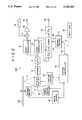
- FIG. 1 is an explanatory views showing an image reproduction of an image information reproducing apparatus.
- FIG. 2 is a block diagram showing a configuration of a first embodiment according to the present invention.
- FIG. 3 is a diagram showing a detailed configuration of a VRAM according to the first embodiment of the present invention.
- FIG. 4 is a flowchart showing the operation of the first embodiment according to the present invention.
- FIG. 5 is an explanatory view showing the operation of the first embodiment according to the present invention.
- FIG. 6 is a diagram showing a passing detection circuit of the present invention.
- FIG. 7 is an explanatory view showing further detailed operation of the first embodiment according to the present invention.
- FIG. 8 is a circuit diagram showing the detailed configuration of a VRAM in a second embodiment of the present invention.
- FIGS. 9 and 10 are explanatory views showing the operation of the second embodiment according to the present invention.
- FIG. 11 is a diagram showing the configuration of a comparative example where a memory of one frame is used.
- FIGS. 12 to 14 are explanatory views showing the operation in the comparative example of the configuration of FIG. 11.
- the LVD musical accompaniment playing apparatus 100 includes a spindle motor 1 for rotationally driving a LVD disc 50 serving as an information recording medium, an optical pick-up 2 for irradiating a laser beam L onto the rotating LVD disk 50 to read out record information recorded on the LVD disk 50 and output it as a read signal, a pre-amplifier 3 for amplifying the read signal read out by the optical pick-up 2, a band-pass filter 4 for separating and extracting, from the amplified read signal, signal in a first frequency band including a frequency band of voice signal and a signal in a second frequency band including a frequency band of video signal, an audio demodulation unit 5 for demodulating audio signal from the extracted first frequency band signal, and a video demodulation unit 6 for demodulating video signal from the extracted second frequency band signal.
- a spindle motor 1 for rotationally driving a LVD disc 50 serving as an information recording medium
- an optical pick-up 2 for irradiating a laser beam L onto the rotating
- This LVD musical accompaniment playing apparatus 100 further includes a microphone 16 for transforming a voice sung in harmony with a played musical accompaniment to a voice signal, a mixer 17 connected to the voice demodulation unit 5 and adapted to mix the voice signal input via the microphone 16 with the demodulated voice signal of musical accompaniment, an amplifier 18 for amplifying the mixed signal, and a voice output terminal 19 for outputting the amplified mixed voice signal.
- This LVD musical accompaniment playing apparatus still further includes an A/D converter 7 for converting the analog video signal demodulated at the video demodulation unit 6 to a digital video signal S 7 , a VRAM 8 for temporarily storing the digital video signal S 7 , a memory control unit 11 for controlling write/read operation of information of the VRAM 8, a D/A converter 9 for converting a digital video signal S 8 read out from the VRAM 8 to an analog video signal, and a video output terminal 20 for outputting the analog video signal.
- A/D converter 7 for converting the analog video signal demodulated at the video demodulation unit 6 to a digital video signal S 7
- VRAM 8 for temporarily storing the digital video signal S 7
- a memory control unit 11 for controlling write/read operation of information of the VRAM 8
- a D/A converter 9 for converting a digital video signal S 8 read out from the VRAM 8 to an analog video signal
- a video output terminal 20 for outputting the analog video signal.
- the LVD musical accompaniment playing apparatus 100 includes a motor control unit 13 for controlling rotation of the spindle motor 1, a laser output control unit 14 for controlling an intensity of laser beam output from the optical pick-up 2, a pick-up control unit 12 for controlling the position and the focal point of the optical pick-up 2, and a system controller 10 for carrying out supervisory control of these respective control units and the memory control unit 11.
- the LVD musical accompaniment playing apparatus 100 includes an input unit 15 connected to the system controller 10 so that various control commands can be input therefrom.
- this VRAM 8 includes frame memories 21 and 22, and changeover switches SW 1 , SW 2 and SW 3 .
- the frame memory 21 includes a field memory 23 for storage of the first field and a field memory 24 for storage of the second field.
- the frame memory 22 includes a field memory 25 for storage of the first field and a field memory 26 for storage of the second field.
- the changeover switch SW 2 includes switching terminals T 1 and T 2
- the changeover switch SW 3 includes switching terminals T 3 and T 4 .
- VRAM 8B includes frame memories 21 and 22, and changeover switches SW 1 and SW 3 .
- the changeover switch SW 3 is connected to the frame memory 21 side (terminal T 3 side) at any time.
- a write control signal CW and a read-out control signal CR are supplied to respective frame memories 21 and 22.
- the write control signal CW includes a write clock, a write V.reset pulse and a write H.reset pulse.
- the read-out control signal CR includes a read clock, a read V.reset pulse and a read H.reset pulse.
- the write clock is a signal synchronous with a burst sub-carrier of the reproduced digital video signal S 7 , and has a frequency (4.fsc) which is four times greater than the sub-carrier frequency of the reproduced video signal (fsc).
- the read clock is a reference clock for reading, and has a frequency four times greater than the sub-carrier (3.58 MHz) of the standard NTSC signal.
- the read-out control signal is generated by a reference signal generator which is not shown.
- the write V.reset pulse is a write reset pulse for the frame memory, produced from the digital video signal S 7 , which resets the write address to zero.
- the write V.reset pulse resets the write address at the leading edge of V. SYNC of the first field.
- the read V.reset pulse resets the read address to zero at the leading edge of V. SYNC of the first field which is generated by the reference signal generator.
- the write H.reset pulse generated from the digital video signal S 7 , is synchronous with the H. SYNC of the reproduced video signal.
- the input video signal is written into the memory at the timing of the write H.reset pulse. Accordingly, the input video signal is regularly written into the memory as shown in FIG. 12.
- the read H.reset pulse is generated from the reference signal generator.
- the video signal written in the memory is read out at the timing of the read H.reset pulse from the corresponding position where the video signal is written.
- the fact that the changeover switch SW 1 is in an open state means that no data is written into the memory.
- the state where no data is written into the memory is realized by allowing the write enable signal WE to be in a disable state, or by stopping supply of the write clock. If the changeover switch SW 1 is actually opened, since the write enable signal WE is in an enable state and the write clock exists, disable data might be written into the memory.
- the write enable signal WE is caused to be at high level to inhibit write operation. If no measure is taken, the upper half of the read-out signal (on the right side of the hatched portion 2 in FIG. 12) becomes an image of frame 1 while the lower half thereof becomes an image of frame 2. However, when the changeover switch SW 1 is opened (WE is caused to be at high level), the image of frame 1 is be read out for all of the read-out image.
- the passing occurs at the intermediate portion of a certain frame (hatched portion of FIG. 14).
- the "passing" means the phenomenon that the read reset pulse passes the write reset pulse. The passing is detected by counting the number of H.reset pulse between the write V.reset pulse and the read V.reset pulse. If the count value becomes less than a predetermined value, the passing will take place in the next frame.
- a frame memory having a memory capacity for at least more than 1.5 frames (three fields) is used.
- two frame memories each having a memory capacity of one frame are used.
- FIG. 4 is a flowchart for explaining the operation of the first embodiment.
- the system controller 10 monitors whether or not a pitch control command instructing a speed control performance is given to the input unit 15 in step 201. If the pitch control command is given, the system controller 10 discriminates whether it is required to insert a frame image in step 202. If the write clock is slower than the read clock, the discrimination in step 202 results in YES. If the discrimination in step 202 results in YES, the system controller discriminates whether or not the passing is detected in step 203.
- the system controller 10 reads out, from the LVD disk 50, image signal of a frame to be inserted (hereinafter referred to as a "frame X" which is assumed to be comprised of a first field A and a second field B) and stores it into both of the frame memories 21 and 22 in the VRAM 8 by the memory control unit 11 in step 204. Then, if the time to insert the frame arrives, the system controller 10 reads out the image signal of the frame X from the field memories 23 and 24 by the memory control unit 11, in the order of the first field A, the first field A, the second field B, and the second field B to output it as a video signal in step 205. Subsequently, the next frame image signal is read from the field memories 25 and 26. Then, it is discriminated that the process is completed or not in step 206.
- a frame X image signal of a frame to be inserted
- step 202 the system controller 10 discriminates whether or not a pitch control processing for which frame omission is required in step 207. If the write clock is faster than the read clock, the discrimination results in YES. If it is discriminated that the frame omission is required in step 207, the operation shifts to step 208 in which it is discriminated that whether or not the time to frame omission arrives. If the discrimination in step 208 results in YES, the system controller 10 omits an image signal of a next frame (i.e., frame (X+1)) and reads out the subsequent frame (i.e., frame (X+2)) from the VRAM 8 to output it as a video signal in step 209. Then, the process proceeds to step 206.
- a next frame i.e., frame (X+1)
- the subsequent frame i.e., frame (X+2)
- the changeover switch SW 1 is closed, and the changeover switch SW 3 is connected to the frame memory 21 side (T 3 side).
- a counter 31 of the passing detection circuit in FIG. 6 (which will be described later) is reset on receiving the read V.reset pulse, the counter counts up the read H.reset pulses until the write V.reset pulse comes to latch that value.
- the latched value is compared with a predetermined value. That is, the counter 31 is reset at the point r of FIG. 14 and latch the number of the read H.reset pulses counted by the point s of FIG. 14.
- FIG. 5 A value latched at the point b of FIG. 5 is judged, and the changeover switch SW 1 is opened for a time period of one frame. After the changeover switch SW 1 is opened, only the data of one frame left in the frame memory 21 is read out (double hatched portions of FIG. 5) and then the changeover switch SW 3 is connected to the frame memory 22 side. After the subsequent one frame is read from the memory 22, the changeover switch SW 3 is connected to the frame memory 21 side.
- FIG. 6 is a block diagram showing a passing detection circuit. Namely, as shown in FIG. 6, the counter 31 is cleared by the read V.reset pulse RV 1 to count up by the read H.reset pulse RH. That count value is latched at the timing of the write V.reset pulse WV 1 normalized by the read clock. Judgment is made in dependency upon whether the latched value is larger or smaller than a predetermined value. It may be possible to count up by the read H.reset pulse RH from the write V.reset pulse until the read V.reset pulse. In such a case, the predetermined value should be changed by subtracting it from 525 which is the number of the fields in a frame image signal.
- FIG. 7 shows in more detail the operation of the first embodiment of FIG. 5.
- a changeover switch SW 2 is added to the circuit of the first embodiment shown in FIG. 3.
- a configuration capable of desirably reading out the contents of field memories 23, 24 in the frame memory 21.
- the content of the field memory 23 (the first field of the first frame) is output twice in succession, and then the content of the field memory 24 (second field of the first frame) is output twice in succession.
- FIG. 8 shows the configuration of a VRAM of the second embodiment.
- the configuration of the entirety of the LVD musical accompaniment playing apparatus is similar to that in the case of the first embodiment.
- the VRAM 8 includes a frame memory 21, a field buffer memory 27, and changeover switches SW 1 , SW 2 , SW 3 and SW 4 .
- the field buffer memory 27 can store video signal of one field.
- the second embodiment differs from the first embodiment shown in FIG. 3 in that the memory capacity is reduced from two frames to the 1.5 frames (3 fields), and that a changeover switch SW 4 is newly added.
- FIG. 9 shows the case where passing occurs at the point j
- FIG. 10 shows the case where passing occurs at the point p.
- the function of the field buffer memory 27 varies in dependency upon where the passing occurs.
- the image of the first field is written into the field buffer memory 27. and the written image is read out at the time of period q of FIG. 10.
- VRAM used in the reproducing speed controller for an image information reproducing apparatus When VRAM used in the reproducing speed controller for an image information reproducing apparatus is constructed as above, the effect equivalent to that of the first embodiment can be obtained by a memory having a memory capacity of 1.5 frames (3 fields).
- the control unit when a speed control command for making the reproducing speed of image information to be low is input, the control unit temporarily stores, into the memories, reproduced image signal at a time when the passing occurs. The passing occurs according to a difference between the speed of write reference signal and the read reference signal. Then, the control unit carries out a control of reproducing image of the first field twice in succession. Then, the control unit carries out a control of reproducing image of the second field twice in succession. Accordingly, display of image at the time of passing is conducted in the order of the first field, the first field, the Second field, and the second field of the insertion frame, resulting no reversal of field images in time. Thus, a picture easy to see, which is free from fluctuation is provided. Namely, this reproducing speed controller for an image information reproducing apparatus can advantageously control the reproducing speed of an image without deterioration of the reproduced image.
Landscapes
- Engineering & Computer Science (AREA)
- Multimedia (AREA)
- Signal Processing (AREA)
- Television Signal Processing For Recording (AREA)
- Reverberation, Karaoke And Other Acoustics (AREA)
- Controls And Circuits For Display Device (AREA)
- Optical Recording Or Reproduction (AREA)
Applications Claiming Priority (2)
| Application Number | Priority Date | Filing Date | Title |
|---|---|---|---|
| JP03344811A JP3083382B2 (ja) | 1991-12-26 | 1991-12-26 | 画像情報再生装置の再生速度制御装置 |
| JP3-344811 | 1991-12-26 |
Publications (1)
| Publication Number | Publication Date |
|---|---|
| US5339167A true US5339167A (en) | 1994-08-16 |
Family
ID=18372165
Family Applications (1)
| Application Number | Title | Priority Date | Filing Date |
|---|---|---|---|
| US07/992,529 Expired - Lifetime US5339167A (en) | 1991-12-26 | 1992-12-17 | Reproduction speed controller for image signal reproducing apparatus |
Country Status (2)
| Country | Link |
|---|---|
| US (1) | US5339167A (ja) |
| JP (1) | JP3083382B2 (ja) |
Cited By (8)
| Publication number | Priority date | Publication date | Assignee | Title |
|---|---|---|---|---|
| US5479265A (en) * | 1992-12-12 | 1995-12-26 | Goldstar Co., Ltd. | Video data recording apparatus for digital video cassette recorder |
| US5557331A (en) * | 1993-03-11 | 1996-09-17 | Matsushita Electric Industrial Co., Ltd. | Image encoding method, an image encoding circuit, an image encoding apparatus, and an optical disk |
| US5748829A (en) * | 1993-05-31 | 1998-05-05 | Asahi Kogaku Kogyo Kabushiki Kaisha | Still image signal processing device employing pedestal level data |
| US5751888A (en) * | 1995-06-06 | 1998-05-12 | Nippon Steel Corporation | Moving picture signal decoder |
| US6020923A (en) * | 1996-07-01 | 2000-02-01 | Sony Corporation | Method and apparatus for coding and recording an image signal and recording medium for storing an image signal |
| US6118546A (en) * | 1995-05-30 | 2000-09-12 | Canon Kabushiki Kaisha | Printer/facsimile driver with page count generation |
| US6356702B1 (en) * | 1997-10-30 | 2002-03-12 | Mitsubishi Denki Kabushiki Kaisha | Image display apparatus and special picture reproduction controller |
| US20190158779A1 (en) * | 2017-11-21 | 2019-05-23 | Vivotek Inc. | Image displaying apparatus and image displaying method |
Families Citing this family (1)
| Publication number | Priority date | Publication date | Assignee | Title |
|---|---|---|---|---|
| JP4040826B2 (ja) | 2000-06-23 | 2008-01-30 | 株式会社東芝 | 画像処理方法および画像表示システム |
Citations (5)
| Publication number | Priority date | Publication date | Assignee | Title |
|---|---|---|---|---|
| US4630132A (en) * | 1982-12-08 | 1986-12-16 | Hitachi, Ltd. | Video signal recording/reproducing apparatus |
| US4774599A (en) * | 1987-01-02 | 1988-09-27 | Eastman Kodak Company | Skip-field video recording with maximum vertical resolution |
| US4864428A (en) * | 1987-02-26 | 1989-09-05 | Pioneer Electronic Corporation | Disk player having variable spindle speed for continuous audio in fast and slow reproduction modes |
| US4959825A (en) * | 1987-06-29 | 1990-09-25 | Pioneer Electronic Corporation | Recorded information reproducing apparatus with reading and writing phase adjustment |
| US5285288A (en) * | 1989-08-25 | 1994-02-08 | Sony Corporation | Video signal reproducing apparatus with time base corrector |
-
1991
- 1991-12-26 JP JP03344811A patent/JP3083382B2/ja not_active Expired - Fee Related
-
1992
- 1992-12-17 US US07/992,529 patent/US5339167A/en not_active Expired - Lifetime
Patent Citations (5)
| Publication number | Priority date | Publication date | Assignee | Title |
|---|---|---|---|---|
| US4630132A (en) * | 1982-12-08 | 1986-12-16 | Hitachi, Ltd. | Video signal recording/reproducing apparatus |
| US4774599A (en) * | 1987-01-02 | 1988-09-27 | Eastman Kodak Company | Skip-field video recording with maximum vertical resolution |
| US4864428A (en) * | 1987-02-26 | 1989-09-05 | Pioneer Electronic Corporation | Disk player having variable spindle speed for continuous audio in fast and slow reproduction modes |
| US4959825A (en) * | 1987-06-29 | 1990-09-25 | Pioneer Electronic Corporation | Recorded information reproducing apparatus with reading and writing phase adjustment |
| US5285288A (en) * | 1989-08-25 | 1994-02-08 | Sony Corporation | Video signal reproducing apparatus with time base corrector |
Cited By (9)
| Publication number | Priority date | Publication date | Assignee | Title |
|---|---|---|---|---|
| US5479265A (en) * | 1992-12-12 | 1995-12-26 | Goldstar Co., Ltd. | Video data recording apparatus for digital video cassette recorder |
| US5557331A (en) * | 1993-03-11 | 1996-09-17 | Matsushita Electric Industrial Co., Ltd. | Image encoding method, an image encoding circuit, an image encoding apparatus, and an optical disk |
| US5748829A (en) * | 1993-05-31 | 1998-05-05 | Asahi Kogaku Kogyo Kabushiki Kaisha | Still image signal processing device employing pedestal level data |
| US6118546A (en) * | 1995-05-30 | 2000-09-12 | Canon Kabushiki Kaisha | Printer/facsimile driver with page count generation |
| US5751888A (en) * | 1995-06-06 | 1998-05-12 | Nippon Steel Corporation | Moving picture signal decoder |
| US6020923A (en) * | 1996-07-01 | 2000-02-01 | Sony Corporation | Method and apparatus for coding and recording an image signal and recording medium for storing an image signal |
| US6356702B1 (en) * | 1997-10-30 | 2002-03-12 | Mitsubishi Denki Kabushiki Kaisha | Image display apparatus and special picture reproduction controller |
| US20190158779A1 (en) * | 2017-11-21 | 2019-05-23 | Vivotek Inc. | Image displaying apparatus and image displaying method |
| US10701306B2 (en) * | 2017-11-21 | 2020-06-30 | Vivotek Inc. | Image displaying apparatus and image displaying method |
Also Published As
| Publication number | Publication date |
|---|---|
| JP3083382B2 (ja) | 2000-09-04 |
| JPH05183877A (ja) | 1993-07-23 |
Similar Documents
| Publication | Publication Date | Title |
|---|---|---|
| CA2033307A1 (en) | Reproducing apparatus for a disc | |
| KR960030678A (ko) | 영상/음성신호를 반도체메모리에 기록/재생하기 위한 장치 | |
| US5339167A (en) | Reproduction speed controller for image signal reproducing apparatus | |
| JPH0345092A (ja) | 磁気テープに記録されているビデオ信号の再生方法及び再生装置 | |
| JPH08107539A (ja) | 情報記録再生装置 | |
| EP0291954B1 (en) | Apparatus for reproducing video signals | |
| US5502572A (en) | Variable speed video signal reproducing apparatus | |
| US5377173A (en) | Jog method for optical disk players having a constant linear velocity | |
| JP2573742B2 (ja) | 音声および画像再生装置 | |
| JPS6256718B2 (ja) | ||
| US5185682A (en) | Recording and/or reproducing apparatus | |
| JP3208034B2 (ja) | 動画像モニタ方法 | |
| JPS63313382A (ja) | プログラム再生装置 | |
| KR100301023B1 (ko) | 기록날자와 기록시간을 제공하는 영상신호 기록/재생방법 및 그 장치 | |
| JPH04286275A (ja) | 静止画像再生装置 | |
| JP2615859B2 (ja) | 記録装置 | |
| KR100585066B1 (ko) | 인덱스 영상을 기록/재생하는 기능을 갖는 vcr | |
| JPH01200790A (ja) | 追加メモリ制御回路 | |
| JP2796715B2 (ja) | 記録再生装置 | |
| JPH07199879A (ja) | 音声対応画像表示装置及び方法 | |
| JPS63158985A (ja) | 磁気記録再生装置 | |
| JPH05265481A (ja) | 自然動画における音声編集装置 | |
| JPH04241244A (ja) | 時間予約記録機能付記録再生装置 | |
| JPS5940383A (ja) | 磁気記録再生装置 | |
| JPH07203371A (ja) | 映像信号処理装置 |
Legal Events
| Date | Code | Title | Description |
|---|---|---|---|
| AS | Assignment |
Owner name: PIONEER ELECTRONIC CORPORATION, JAPAN Free format text: ASSIGNMENT OF ASSIGNORS INTEREST.;ASSIGNOR:KURODA, KAZUO;REEL/FRAME:006350/0955 Effective date: 19921207 |
|
| STCF | Information on status: patent grant |
Free format text: PATENTED CASE |
|
| FPAY | Fee payment |
Year of fee payment: 4 |
|
| FPAY | Fee payment |
Year of fee payment: 8 |
|
| FEPP | Fee payment procedure |
Free format text: PAYOR NUMBER ASSIGNED (ORIGINAL EVENT CODE: ASPN); ENTITY STATUS OF PATENT OWNER: LARGE ENTITY |
|
| FPAY | Fee payment |
Year of fee payment: 12 |