US5260824A - Atomic force microscope - Google Patents
Atomic force microscope Download PDFInfo
- Publication number
- US5260824A US5260824A US07/511,054 US51105490A US5260824A US 5260824 A US5260824 A US 5260824A US 51105490 A US51105490 A US 51105490A US 5260824 A US5260824 A US 5260824A
- Authority
- US
- United States
- Prior art keywords
- cantilever
- probe
- specimen
- light
- atomic force
- Prior art date
- Legal status (The legal status is an assumption and is not a legal conclusion. Google has not performed a legal analysis and makes no representation as to the accuracy of the status listed.)
- Expired - Lifetime
Links
Images


Classifications
-
- G—PHYSICS
- G01—MEASURING; TESTING
- G01Q—SCANNING-PROBE TECHNIQUES OR APPARATUS; APPLICATIONS OF SCANNING-PROBE TECHNIQUES, e.g. SCANNING PROBE MICROSCOPY [SPM]
- G01Q60/00—Particular types of SPM [Scanning Probe Microscopy] or microscopes; Essential components thereof
- G01Q60/24—AFM [Atomic Force Microscopy] or apparatus therefor, e.g. AFM probes
- G01Q60/38—Probes, their manufacture, or their related instrumentation, e.g. holders
-
- G—PHYSICS
- G01—MEASURING; TESTING
- G01Q—SCANNING-PROBE TECHNIQUES OR APPARATUS; APPLICATIONS OF SCANNING-PROBE TECHNIQUES, e.g. SCANNING PROBE MICROSCOPY [SPM]
- G01Q20/00—Monitoring the movement or position of the probe
- G01Q20/02—Monitoring the movement or position of the probe by optical means
-
- G—PHYSICS
- G01—MEASURING; TESTING
- G01Q—SCANNING-PROBE TECHNIQUES OR APPARATUS; APPLICATIONS OF SCANNING-PROBE TECHNIQUES, e.g. SCANNING PROBE MICROSCOPY [SPM]
- G01Q30/00—Auxiliary means serving to assist or improve the scanning probe techniques or apparatus, e.g. display or data processing devices
- G01Q30/02—Non-SPM analysing devices, e.g. SEM [Scanning Electron Microscope], spectrometer or optical microscope
- G01Q30/025—Optical microscopes coupled with SPM
-
- Y—GENERAL TAGGING OF NEW TECHNOLOGICAL DEVELOPMENTS; GENERAL TAGGING OF CROSS-SECTIONAL TECHNOLOGIES SPANNING OVER SEVERAL SECTIONS OF THE IPC; TECHNICAL SUBJECTS COVERED BY FORMER USPC CROSS-REFERENCE ART COLLECTIONS [XRACs] AND DIGESTS
- Y10—TECHNICAL SUBJECTS COVERED BY FORMER USPC
- Y10S—TECHNICAL SUBJECTS COVERED BY FORMER USPC CROSS-REFERENCE ART COLLECTIONS [XRACs] AND DIGESTS
- Y10S977/00—Nanotechnology
- Y10S977/84—Manufacture, treatment, or detection of nanostructure
- Y10S977/849—Manufacture, treatment, or detection of nanostructure with scanning probe
- Y10S977/86—Scanning probe structure
- Y10S977/868—Scanning probe structure with optical means
- Y10S977/87—Optical lever arm for reflecting light
Definitions
- the present invention relates to an atomic force microscope.
- the atomic force microscope detects the displacement of the cantilever, for the measurement of the atomic force acting between the atoms of the tip end of the probe and the atoms of the specimen surface.
- the atomic force microscope also allows atom-level observation of the specimen surface by scanning the specimen surface with the probe, with the interatomic force maintained at a constant value.
- An example of such an atomic force microscope is described in a treatise by G. Binnig, C. F. Quate, Ch. Gerber, et al. (Physical Review Letters Vol. LVI, No. 9 [March 1986], pp 930-933).
- Known methods for detecting the displacement of the cantilever includes: a method using a scanning tunnel microscope (STM), an electrostatic capacitance method, a photo detection method, etc.
- STM scanning tunnel microscope
- a tunnel probe is attached to one side (the obverse side) of a cantilever such that the distance between the tunnel probe and the other side (the reverse side) of the cantilever is short enough to permit a tunnel current to flow therebetween.
- the displacement of the cantilever is measured on the basis of variations in the tunnel current.
- a plate capacitor is formed such that its one pole plate is constituted by the reverse side of a cantilever (the reverse side being a side opposite to that where a probe is attached).
- the displacement of the cantilever is measured on the basis of variations in the electrostatic capacitance.
- the reverse side of a cantilever is formed to have an optically-reflecting face.
- This optically-reflecting face is irradiated with a laser beam.
- a variation which the angle of reflection of the laser beam may have in accordance with the displacement of the cantilever and a variation which the interference fringe may have when the laser beam reflected by the optically-reflecting surface is returned to an interferometer, are detected.
- the displacement of the cantilever is measured.
- the scanning tunnel microscope comprises a transparent glass plate which is arranged in a plane perpendicular to the observation optical axis of the optical microscope.
- An STM probe is placed upright on the transparent glass plate in parallel to the observation optical axis, such that the STM probe does not block the vision field of the optical microscope.
- the technique of confirming a measurement portion by use of the optical microscope is useful not only to the STM but also to the AFM.
- the STM largely occupies the vision field of the optical microscope.
- the plate capacitor occupies a certain area of the cantilever, so that the area of the cantilever has to be increased to a certain extent. Accordingly, a large space is required in parallel to the surface of a specimen.
- an object of the present invention is to provide an atomic force microscope enabling a measurement portion to be visually confirmed in a reliable manner by use of an optical microscope.
- a probe supported close to the surface of the specimen and having a tip end for producing an interatomic force with reference to the surface of the specimen;
- a cantilever having a free end portion on which the probe is supported, the cantilever being elastically deformable and displacing the free end portion thereof in accordance with an interatomic force acting between an atom of the tip end of the probe and an atom of the surface of the specimen;
- a detection optical system for irradiating the cantilever with detecting light, so as to detect the displacement of the cantilever.
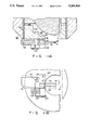
- FIG. 1 is a partially-sectional front view showing an atomic force microscope according to the first embodiment of the present invention
- FIG. 2 is a partially-sectional side view of the atomic force microscope shown in FIG. 1;
- FIG. 3 is a view showing an optical system used for measurement of a probe displacement and an optical system used for observation of a specimen surface, both optical systems being incorporated in the atomic force microscope shown in FIGS. 1 and 2;
- FIG. 4 is a view illustrating the critical angle method used in the probe displacement-measuring optical system shown in FIG. 3;
- FIG. 5 is a block circuit diagram of a signal-processing circuit which is used for the critical angle method illustrated in FIG. 4;
- FIGS. 6A and 6B are plan and side views, respectively, of a cantilever employed in the atomic force microscope shown in FIGS. 1 and 2;
- FIG. 7 is a view of another type of cantilever which can be employed in the atomic force microscope shown in FIGS. 1 and 2;
- FIGS. 8A to 8C are views illustrating the process in which the cantilever shown in FIG. 7 is formed
- FIGS. 9A to 9C are views illustrating the process in which the probes shown in FIGS. 6B and 7 are formed;
- FIG. 10 is a view of the reticle used in the probe displacement-measuring optical system
- FIGS. 11A and 1B are sectional and bottom views, respectively, showing a modification of the probe-driving system employed in the atomic force microscope shown in FIGS. 1 and 2;
- FIG. 12 is a view showing another modification of the cantilever-driving system employed in the atomic force microscope shown in FIGS. 1 and 2;
- FIG. 13 is view showing one type of cantilever employed in an atomic force microscope according to the second embodiment of the present invention, the cantilever allowing not only sample observation using an interatomic force but also sample observation based on the optical principles;
- FIG. 14 is view showing another type of cantilever which can be employed in the atomic force microscope according to the second embodiment of the present invention, the cantilever allowing not only sample observation using an interatomic force but also sample observation based on the optical principles.
- an apparatus 10 i.e., a microscope
- a specimen stage-moving mechanism 12 a probe-driving system 14, a probe displacement-measuring optical system 16, and a specimen surface-observing optical system 18.
- the specimen stage-moving mechanism 12 is mounted on a vibration-proof base 30 which is pressure-controlled by use of e.g. an air spring.
- the specimen stage-moving mechanism 12 comprises an XY stage 35.
- This XY stage 35 is arranged in the space which is defined by: a rectangular base member 31 placed on the vibration-proof base 30; support poles 32a, 32b standing upright on the respective corners of the base member 31; and a support base plate 33 which is fixed to the tops of the support poles 32a, 32b by means of bolts 34.
- the XY stage 35 includes an X-axis base seat 36, on which a slide plate 37 for determining an X-axis position is provided such that it is slidable in an X-axis direction (which is indicated by X in FIG. 1).
- the XY stage 35 also includes a Y-axis base seat 38, on which a slide plate 39 for determining a Y-axis position is provided such that it is slidable in a Y-axis direction (which is indicated by Y in FIG. 2).
- an operation rod 40a When an X-axis operation dial 40 is rotated, an operation rod 40a is advanced or retreated by a feed screw mechanism (not shown), with the result that the slide plate 37 for determining in an X-axis position is slid for coarse adjustment.
- a Y-axis operation dial 41 When a Y-axis operation dial 41 is rotated, an operation rod 41a is advanced or retreated by a feed screw mechanism (not shown), with the result that the slide plate 39 for determining in a Y-axis position is slid for coarse adjustment.
- a lamination-type piezoelectric actuator 42 used for a Y-axis direction scan is mounted on the slide plate 39. With a driving force produced by the actuator 42, a Y table 43 is moved for fine adjustment in the Y-axis direction along the surface of the slide plate 39.
- a lamination-type piezoelectric actuator 44 used for a X-axis direction scan is mounted on the Y table 43. With a driving force produced by the actuator 44, an X table 45 is moved for fine adjustment in the X-axis direction along the surface of the X table 45.
- the maximum distance along which the X table 45 and the Y table 43, respectively, are position-controlled is 50 ⁇ m.
- a so-called tripod 46 i.e., a fine-adjustment element
- a specimen stage 51 on which a specimen 20 is to be placed is attached to the tripod 46, with a support member 46b interposed.
- the three piezoelectric bodies 46a of the tripod 46 extend in the X-axis, Y-axis, and Z-directions, respectively. They are secured, at one end, to the support member 46b (which is attached to the lower side of the specimen stage 51), and are secured, at the other end, to three wall portions (which are perpendicular to one another) of the base portion 46c of the tripod 46, respectively.
- the specimen stage 51 is moved relative to the X table 45 in the X-axis, Y-axis, and Z-axis directions within the range of less than 15 ⁇ m.
- the upper side of the specimen stage 51 is located within a hole formed in the center of the support base plate 33, and the specimen 20 is placed on the upper side of the specimen stage 51.
- a column 53 having a horizontally-extending motor support plate 54 on top, is fixed to that portion of the support base plate 33 which is located above the support pole 32b.
- a motor 55 is fixed to the motor support plate 54, with its rotating shaft extending vertically.
- a manual rotation disk 56 which has an operation pin 57 projected from a circumferential portion thereof and used for coarse adjustment (i.e., fast-feed adjustment), is attached to the upwardly-projected portion of the rotating shaft of the motor 55.
- the downwardly-projected portion of the rotating shaft of the motor 55 extends through a friction coupling 58, is vertically held by a holding piece 53a of the column 53 in a rotatable manner, and is coupled to a shaft 59.
- This shaft 59 has a feed screw portion threadably engaged with the feed nut 60a of an optical system holder 60.
- the optical system holder 60 has a holding piece 60b attached to a proximal end portion of an optical headmounting plate 62.
- the side portions of this mounting plate 62 are coupled to respective linear slide bearing mechanisms 64, which are provided on top of support poles 63 standing upright on the support base plate 33.
- Each linear slide bearing mechanism 64 comprises a case screwed on the mounting plate 62 and a slide bearing arranged inside the case.
- Each linear slide bearing mechanism 64 is fitted around the outer wall of the corresponding support pole 63.
- the lower end of each linear slide bearing mechanism 64 is fixed to the support pole 63 by means of a lock screw 65.
- a specimen surface-observing optical system 18 (which includes a microscope eyepiece section 66, a video camera-mounting cylinder 67, an illuminator 68 for observation, etc.) is fixed to the upper side of the mounting plate 62.
- a probe displacement-measuring optical system 16 (which includes an objective lens 83) and a probe-driving system 14 are arranged below the mounting plate 62.
- the probe displacement-measuring optical system 16 is fixed to, and is detachable from, the mounting block 81 of a fine-adjustment driving device 80 movable along one axis.
- the mounting block 81 can be vertically moved by a lamination-type piezoelectric actuator 82, which is fixed to the vertical plate 60c of the optical system holder 60.
- the probe displacement-measuring optical system 16 can be slightly moved in the vertical direction by the lamination-type piezoelectric actuator 82.
- the specimen surface-observing optical system 18 and the probe displacement-measuring optical system 16 will be described, with reference to FIG. 3.
- the illuminating light emitted from the light source of the illuminator 68 is first collimated by a lens 97 and is then reflected downward by a half-mirror 92.
- the illuminating light reflected by the half mirror 92 passes via a filter 91, a half-mirror 85 and a quarter wavelength plate 84, and falls on an objective lens 83.
- the entire specimen 20 is illuminated.
- the light reflected by the specimen 20 passes via the objective lens 83, the quarter wavelength plate 84, the half-mirror 85 and the half-mirror 92, and then falls on a light-focusing lens 93.
- the light-focusing lens 93 By this light-focusing lens 93, the light is made to be incident on a prism 94. Part of the light incident on the prism 94 is reflected by a surface of the prism 94, such that it enters an eye-piece 95. The remaining part of the light passes through the prism 94, so that it enters a video camera 98 incorporating a CCD element or the like. In the video camera 98 the light is converted into a video signal, and this video signal is supplied to a video monitor 99 for visualizing the video signal.
- the quarter wavelength plate 84 is slightly slanted with reference to the optical path such that the light reflected by the specimen 20 does not directly enter the specimen surface-observing optical system 18. Accordingly, the image within the field of vision is clear and free of flare.
- the laser beam emitted from the laser diode 87 of the probe displacement-measuring optical system 16 is first collimated by a collimating lens 90 and is then incident on a polarized beam-splitter 86.
- the laser beam reflected by this splitter 86 is further reflected by the half-mirror 85, and is incident on the quarter wavelength plate 84.
- the quarter wavelength plate 84 When passing through the quarter wavelength plate 84, the laser beam is converted from linearly-polarized light into circularly-polarized light.
- the laser beam, thus converted, is converged on the upper side of the cantilever 22 by the objective lens 83, such that the point of convergence is located at the probe 21.
- the laser beam reflected by the upper side of the cantilever 22 passes through the objective lens 83 and the quarter wavelength plate 84, and is reflected by the half-mirror 85 toward the polarized beam-splitter 86.
- the laser beam reflected by the cantilever 22 is converted back into linearly-polarized light, such that the vibration plane of the laser beam which is output from the quarter wavelength plate 84 is rotated 90° from that of the laser beam which is input to the quarter wavelength plate 84.
- the laser beam reflected by the half-mirror 85 and entering the polarized beam-splitter 86 is split into two laser beams.
- One of these two laser beams is incident on a first two-component light-receiving element 89a after passing through a first critical angle prism 88a, while the other laser beam is incident on a second two-component light-receiving element 89b after passing through a second critical angle prism 88b.
- a critical angle method is utilized for detecting the position of the cantilever 22.
- the principles underlying the critical angle method will be explained briefly, with reference to FIGS. 4 and 5.
- a critical angle prism c is arranged such that its reflecting surface forms a critical angle with reference to the collimated light rays coming from a lens b.
- the reflecting surface a of a given object When the reflecting surface a of a given object is located at the position indicated by solid line B in FIG. 4 (i.e., when the beam is in focus), the light beam reflected by reflecting surface a is collimated by the lens b and is then incident on the critical angle prism c. The light beam is totally reflected by the reflecting surface of the prism c, and the same amount of light is directed to each photodiode of a two-component light-receiving element.
- the reflecting surface a When the reflecting surface a is located at the position indicated by broken line C in FIG. 4 (i.e., when the reflecting surface a is closer to the lens b than the focal point of the lens b), the light beam reflected by the reflecting surface a becomes a divergent light beam when passing through the lens b, and is then incident on the critical angle prism c. Conversely, when the reflecting surface a is located at the position indicated by broken line A in FIG. 4 (i.e., when the reflecting surface is more away from the lens b than the focal point of the lens b), the light beam reflected by reflecting surface a becomes a convergent light beam when passing through the lens b, and is then incident on the critical angle prism c.
- the light bean incident on the critical angle prism c is not a collimated light beam. Therefore, only the central rays of the light beam are incident on the prism c at the critical angle.
- the rays passing along one side of the central rays are incident on the prism c at an angle narrower than the critical angle, so that part of them are directed to the outside of the prism c, with the remaining part being reflected by the prism c.
- the rays passing along the other side of the central rays are incident on the prism c at an angle wider than the critical angle, so that they are totally reflected by the prism c.
- the light amount which one photodiode receives differs from the light amount which the other receives.
- a signal corresponding to the difference in the light amount is produced from an output terminal f after being amplified by a differential amplifier e. That is, the position of the reflecting surface a is detected as the light amount difference between the detecting portions of the two-component light-receiving element d.
- An output of one photodiode PD1 of the first light-receiving element is supplied to the inversion input terminal of a comparator 102, and an output of the other photodiode PD2 is supplied to the non-inversion input terminal of the same comparator 102.
- the comparator 102 produces a signal corresponding to the difference between the outputs of photodiodes PD1 and PD2.
- an output of one photodiode PD3 of the second light-receiving element is supplied to the inversion input terminal of a comparator 104, and an output of the other photodiode PD4 is supplied to the non-inversion input terminal of the same comparator 104.
- the comparator 104 produces a signal corresponding to the difference between the outputs of photodiodes PD3 and photodiode PD4 is produced from the comparator 104.
- the signals produced from the comparators 102 and 104 are added together, and a signal obtained by this addition is supplied to one of the paired input terminals of a comparator 106, where it is compared with a reference value. A result of this comparison is output from the comparator 106.
- a signal corresponding to the light amount difference between the region on one side of the beam spot on the two-component light-receiving element and the region on the other side of the beam spot (the signal represents the position of the cantilever 22) is output from a terminal 108.
- the probe-driving system 14 of the probe displacement-measuring optical system 16 is made up of: a cantilever 22 having a probe 21 thereon; a tripod 23 for slightly moving the cantilever 22; and a mechanism for inserting the cantilever 22 into the region between the objective lens 83 and the specimen 20 and for pulling the cantilever 22 out of the region.
- the probe 21 is located at the free end of the cantilever 22, and the other end of the cantilever 22 is supported by the support member 23b of a tripod 23 (which includes piezoelectric bodies 23a perpendicular to one another).
- the tripod 23 is supported, at its base portion 23c, by a member 24 slidably provided for a holder 25.
- the tripod 23 can be moved in the lateral direction, as viewed from FIG. 1, by a driving rod 27 moved by a pulse motor 26. With this construction, the probe 21 can be inserted into the region between the objective lens 83 and the specimen 20 or pulled out of the region.
- the cantilever 22 has a diamond or tungsten stylus on one side thereof, and this stylus serves as the probe 21 mentioned above.
- a mark 28 is formed by use of lithography, so as to indicate the tip point of the probe 21.
- FIG. 7 shows an example of another type of cantilever which can be used in the present invention.
- the cantilever 22 is formed of Si, and the probe 21 and the mark 28, which are on the respective sides of the free end of the cantilever 22, are formed by use of micro fabrication.
- the "micro fabrication” is also called micro machining or micro dynamics, and refers to the technique developed on the basis of the semiconductor device-manufacturing technology.
- micro fabrication it does not indicate a technique for manufacturing a purely electrical device, such as an IC, but indicates a technique for manufacturing a device of which mechanical movement is required or whose mechanical shape plays an important role.
- the technique mentioned in Kurt E. Petersen, "Silicon As a Mechanical Material. Proceedings of the ITTT" 70(1982)420 may be regarded as micro fabrication.
- Anisotropic etching and isotropic etching are typical examples of major processes utilized in the micro fabrication.
- the cantilever 22 employed in the atomic force microscope should be thin and light in weight, so as to make the most of the movement of the probe 21. At the same time, however, its support portion 22a should have a certain mechanical strength, for easy attachment of the cantilever 22 to the microscope or for easily replacement of the cantilever 22 with another one.
- a cantilever support plate is employed in the present invention. The thickness of this cantilever support plate is nearly equal to the thickness of an Si wafer used for the formation of the cantilever.
- FIGS. 8A to 8C A description may now be given as to how the cantilever 22 is manufactured, with reference to FIGS. 8A to 8C.
- the lower side (i.e., the reverse side) of an Si wafer 70 is anisotropically etched, using Si 3 N 4 as a mask (FIG. 8A).
- an optical reflection film 29 is formed on the upper side of the Si wafer 70.
- the lower side of the Si wafer 70 oxidizes in the ambient atmosphere, so that an SiO 2 film 71 is formed on the lower side.
- a mark 28 and a probe 21 are formed, as explained below, on a thin portion obtained by the anisotropic etching, such that the mark 28 is on the upper side and the probe 21 is on the lower side (FIG. 8B).
- the Si wafer 70 is etched from the lower side by use of reactive ion plasma, to thereby cut a cantilever portion from the Si wafer 70. In this manner, the cantilever 22 shown in FIG. 7 is manufactured
- the probe and the mark can be simultaneously formed in the same process. Since, therefore, the probe and the mark can be accurately aligned in the vertical direction, the cantilever is permitted to have intended dimensions. In addition, cantilevers having uniform quality can be manufactured for replacement use.
- a mask pattern 73 having a hole 74 is prepared. This mask pattern 73 is arranged close to that side of the Si wafer 70 for which the probe 21 or mask 28 is to be formed, as is shown in FIG. 9A.
- a conductive material is deposited over the Si wafer 70 from the direction indicated by the arrows in FIG. 9B.
- a mark 28 is formed on the Si wafer 70 by stopping the deposition when the conductive material 76 deposited on the Si wafer 70 is still in the shape of a truncated cone (FIG. 9B).
- the deposition is continued until the hole 74 is completely filled with the conductive material 76 deposited over the mask 73. By so doing, the probe 21 is formed to have a conical shape, as is shown in FIG. 9C.
- the material of the cantilever is not limited to Si; it may be determined in accordance with the manner in which the microscope is used.
- the cantilever was described as being manufactured by the etching of the Si wafer 70.
- the base portion of the Si wafer 70 may be further etched in such a manner that the cantilever is constituted by a thin film of SiO 2 , Si 3 N 4 , polycrystalline Si, Al, etc., which are obtained by combination of both an etching technique and a film deposition technique (such as CVD, deposition, sputtering, or the like).
- the cantilever 22 is moved to the region within the visual, field of the optical microscope by use of the pulse motor 26 and the tripod 23. Then, the cantilever 22 is adjusted such that its mark 28 is located in the center of the cross-shaped lines 78 of the reticle 77 (FIG. 10) of the optical microscope, and the adjusted position of the cantilever is recorded on the basis of the pulse count of the pulse motor and/or the voltage applied to the tripod 23. In the case where the video camera 98 is used, the cantilever 22 is adjusted such that its mark 28 is located in the center of the cross-shaped cursor of the video monitor 99.
- the cantilever 22 is moved out of the visual field of the optical microscope by use of the pulse motor 26.
- the XY stage 35 is driven until a measurement portion (i.e., a portion to be measured) of the specimen 20 is located in the center of the cross-shaped lines 78 or the cross-shaped cursor.
- the tripod 46 and the specimen stage-moving mechanism 12 are kept locked until AFM measurement (i.e., measurement employing an atomic force microscope) is performed.
- the mark 28 of the cantilever 22 is adjusted again to the center of the cross-shaped lines 78, on the basis of the recorded pulse count and/or the recorded voltage.
- the tip end of the probe 21 of the cantilever 22 can be adjusted to the measurement portion of the specimen 20.
- a two-dimensional scan is carried out by use of the tripod 23 or 46.
- the displacement of the cantilever 22 (the displacement being caused due to the force acting between the atoms of the tip end of the probe 21 and one atom of the specimen 20) is measured by the probe displacement-measuring optical system 16. The measured displacement is shown on a CRT monitor.
- the cantilever 22 can be inserted or pulled out of the region between the objective lens 83 and the specimen 20 not only by the mechanism mentioned above but also by the mechanism shown in FIGS. 11A and 11B.
- a cantilever 22 has a mark 28 and a probe 21 formed on the respective sides thereof.
- the cantilever 22 has a support portion 115 clamped by use of three thin plates 116, 117 and 118, and an arm portion 112 projected from the thin plates 116, 117 and 118.
- the thin plates 116, 117 and 118 have a common hole 119, in which a shaft 121 extending through the hole 119 of a fixed ring 120 is inserted.
- a slip ring 126 is fitted around the shaft 121, and this slip ring 126 supports the thin plates 116, 117 and 118 such that the cantilever 22 can be rotated.
- the fixed ring 120 has a spring stopper 123 for securing an L-shaped spring 122.
- One end of the L-shaped spring 122 abuts a stopper block 124, and the cantilever 22 is prevented from rotating beyond a certain position in the clockwise direction indicated by arrow R in FIG. 11A.
- the fixed ring 120 also has a positioning block 125.
- This positioning block 125 abuts the cantilever 22, so that the position of the cantilever 22 can be accurately determined with reference to the counterclockwise rotation (indicated by arrow L in FIG 11A) of the L-shaped spring 122.
- the fixed ring 120 has a male screw portion 127 extending perpendicular to the cantilever 22, and this male screw portion 127 is engageable with the female screw portion 128 of the objective lens 83.
- its mark 28 (FIG. 10) is located in the center of the cross-shaped lines of the reticle.
- the cantilever 22 of this embodiment can be easily moved out of the vision field by rotating the end portions of the thin plates 116-118 (which are located on a line extending from the support portion 115) clockwise with fingers or by use of suitable means.
- FIG. 12 shows still another mechanism which can be used for inserting the cantilever 22 into the region between the objective lens 83 and the specimen 20 or for pulling the cantilever 22 out of the region.
- a spring 129 is located between the cantilever 22 and the tripod 23.
- the spring 129 is thin if viewed from above, and can be curved in the horizontal direction. Therefore, the cantilever 22 is permitted to horizontally swing, with the tripod 23 as a center. Since the spring 129 is not allowed to curve in the vertical direction, it does not have any adverse effects on the displacement of the cantilever 22.
- the probe 21 can be moved out of the vision field of the optical system by applying an external force to the spring 129 in the curving direction thereof by use of a suitable means (not shown). The probe 21 elastically returns to the original position by releasing the spring from the external force.
- the cantilever 22 and probe 21 used in this alternative embodiment are shown in FIG. 13.
- the cantilever 22 has a specularly-polished surface on the upper side of the distal end portion thereof. From the lower side of the distal end portion of the cantilever 22, the probe 21 extends slantwise in the downward direction such that its tip end looks projected from the distal end of the cantilever, if viewed from above.
- the illuminating light of the specimen surface-observing optical system 18 is made to fall on the tip end of the probe 21, while the laser beam of the probe displacement-measuring optical system 16 is made to fall on the free end portion (i.e., the distal end portion) of the cantilever 22.
- the optical path of the illuminating light of the optical system 18 and that of the laser beam of the optical system 16 are different. With this construction, a specimen 20 can be optically observed, simultaneous with the detection of the displacement of the probe 21.
- the probe-driving system 14 of the above embodiment does not have to employ a mechanism for inserting the cantilever 22 or retracting it from the region between the objective lens 83 and the specimen 20.
- the cantilever 22 may be secured to the region near a hole 52 by use of a piezoelectric member.
- the way for observing a specimen 20 will be described.
- the specimen 20 is first placed on the specimen stage 51, and then the specimen surface-observing optical system 18 is focused on the specimen 20 by operating the coarse-adjustment operation pin 57, the manual rotation disk 56, the motor 55, etc.
- the displacement-measuring optical system 16 is turned on to drive the piezoelectric bodies, and is focused on the upper side of the cantilever.
- the tripod is driven, so as to move the specimen stage 51 upward.
- an output of the measuring optical system 16 slightly varies.
- the upward movement of the tripod is stopped, to thereby maintain the state wherein the cantilever is kept applied with the force arising from the interatomic force. In this state, the specimen 20 is scanned.
- a signal voltage for producing reciprocating motion is applied to the X-axis direction piezoelectric body of the tripod 46, and a signal voltage for producing linear motion is applied to Y-axis direction piezoelectric body of the tripod 46.
- the specimen 20 is XY raster scanned.
- the measurement is continued until a predetermined region of the specimen 20 is scanned.
- the Z-axis direction piezoelectric body of the tripod 46 is feedback-controlled such that the inclination of the cantilever is maintained at a constant value.
- a fine profile of the surface of the specimen is measured.
- the probe 21 employed in the above embodiment is projected from the distal end of the cantilever 22. Therefore, the light for illuminating the vision field falls on the field under observation, without being intercepted by the cantilever 22. Accordingly, the surface profile under measurement can be optically observed while the fine surface profile of the specimen is being measured by the probe 21.
- FIG. 14 shows another type of cantilever 22 and another type of probe 21 which can be employed in the above embodiment.
- the cantilever 22 and probe 21 shown in FIG. 14 none of the specimen stage-moving mechanism 12, the displacement-measuring optical system 16 and the specimen surface-observing optical system 18 have to be specially modified, and a fine profile of the specimen surface can be measured by following similar procedure to that mentioned above.
- the cantilever 22 has a tapered distal end portion.
- the probe 21, with which to examine the specimen surface is supported on the lower side of the tapered distal end and extends slantwise in the downward direction. In the case of the modification shown in FIG.
- the illuminating light of the optical system 18 and the laser beam of the optical system 16 pass along the same optical path, and the laser beam is converged on the upper side of the cantilever 22 such that the point of convergence is located just above the tip end of the probe 21.
- the displacement of the distal end portion of the cantilever accurately reflects the displacement of the tip end of the probe, so that it is not necessary to perform a correcting operation.
- the illuminating light is intercepted by the distal end of the cantilever 22, an observation image can be sufficiently clear since the distal end of the cantilever 22 is tapered and has only a small area.
Applications Claiming Priority (6)
| Application Number | Priority Date | Filing Date | Title |
|---|---|---|---|
| JP10402889A JPH02281103A (ja) | 1989-04-24 | 1989-04-24 | 原子間力顕微鏡 |
| JP1-104028 | 1989-04-24 | ||
| JP1-207738 | 1989-08-10 | ||
| JP1207738A JP2791121B2 (ja) | 1989-08-10 | 1989-08-10 | 微細表面形状計測装置 |
| JP1240310A JPH03102209A (ja) | 1989-09-16 | 1989-09-16 | 原子間力顕微鏡 |
| JP1-240310 | 1989-09-16 |
Publications (1)
| Publication Number | Publication Date |
|---|---|
| US5260824A true US5260824A (en) | 1993-11-09 |
Family
ID=27310130
Family Applications (1)
| Application Number | Title | Priority Date | Filing Date |
|---|---|---|---|
| US07/511,054 Expired - Lifetime US5260824A (en) | 1989-04-24 | 1990-04-19 | Atomic force microscope |
Country Status (3)
| Country | Link |
|---|---|
| US (1) | US5260824A (de) |
| EP (1) | EP0394962B1 (de) |
| DE (1) | DE69010552T2 (de) |
Cited By (64)
| Publication number | Priority date | Publication date | Assignee | Title |
|---|---|---|---|---|
| US5406833A (en) * | 1992-09-02 | 1995-04-18 | Seiko Instruments, Inc. | Atomic force microscope |
| US5440920A (en) * | 1994-02-03 | 1995-08-15 | Molecular Imaging Systems | Scanning force microscope with beam tracking lens |
| US5463897A (en) * | 1993-08-17 | 1995-11-07 | Digital Instruments, Inc. | Scanning stylus atomic force microscope with cantilever tracking and optical access |
| US5481527A (en) * | 1992-03-31 | 1996-01-02 | Canon Kabushiki Kaisha | Information processing apparatus with ferroelectric rewritable recording medium |
| US5515719A (en) * | 1994-05-19 | 1996-05-14 | Molecular Imaging Corporation | Controlled force microscope for operation in liquids |
| USRE35317E (en) * | 1991-07-26 | 1996-08-27 | The Arizona Board Of Regents | Potentiostatic preparation of molecular adsorbates for scanning probe microscopy |
| US5612491A (en) * | 1994-05-19 | 1997-03-18 | Molecular Imaging Corporation | Formation of a magnetic film on an atomic force microscope cantilever |
| US5621210A (en) * | 1995-02-10 | 1997-04-15 | Molecular Imaging Corporation | Microscope for force and tunneling microscopy in liquids |
| USRE35514E (en) * | 1991-03-13 | 1997-05-20 | Park Scientific Instruments | Scanning force microscope having aligning and adjusting means |
| US5654546A (en) * | 1995-11-07 | 1997-08-05 | Molecular Imaging Corporation | Variable temperature scanning probe microscope based on a peltier device |
| US5675154A (en) * | 1995-02-10 | 1997-10-07 | Molecular Imaging Corporation | Scanning probe microscope |
| US5714756A (en) * | 1992-03-13 | 1998-02-03 | Park Scientific Instruments | Scanning probe microscope having a single viewing device for on-axis and oblique angle views |
| US5750989A (en) * | 1995-02-10 | 1998-05-12 | Molecular Imaging Corporation | Scanning probe microscope for use in fluids |
| US5753814A (en) * | 1994-05-19 | 1998-05-19 | Molecular Imaging Corporation | Magnetically-oscillated probe microscope for operation in liquids |
| US5756997A (en) * | 1996-03-04 | 1998-05-26 | General Nanotechnology, L.L.C. | Scanning probe/optical microscope with modular objective/probe and drive/detector units |
| US5821545A (en) * | 1995-11-07 | 1998-10-13 | Molecular Imaging Corporation | Heated stage for a scanning probe microscope |
| US5825020A (en) * | 1996-09-06 | 1998-10-20 | The Regents Of The University Of California | Atomic force microscope for generating a small incident beam spot |
| US5834644A (en) * | 1995-11-13 | 1998-11-10 | The University Of Virginia Patent Foundation | Automatic atomic force microscope with piezotube scanner |
| US5850038A (en) * | 1995-12-14 | 1998-12-15 | Olympus Optical Co., Ltd. | Scanning probe microscope incorporating an optical microscope |
| US5852233A (en) * | 1993-07-26 | 1998-12-22 | Fraunhofer-Gesellschaft Zur Forderung Der Angewandten Forschung E.V. | Acoustic microscope with a control and data capturing device |
| US5859364A (en) * | 1995-06-05 | 1999-01-12 | Olympus Optical Co., Ltd. | Scanning probe microscope |
| US5861550A (en) * | 1997-10-14 | 1999-01-19 | Raymax Technology, Incorporated | Scanning force microscope |
| US5866805A (en) * | 1994-05-19 | 1999-02-02 | Molecular Imaging Corporation Arizona Board Of Regents | Cantilevers for a magnetically driven atomic force microscope |
| US5874669A (en) * | 1997-10-16 | 1999-02-23 | Raymax Technology, Inc. | Scanning force microscope with removable probe illuminator assembly |
| US5874668A (en) * | 1995-10-24 | 1999-02-23 | Arch Development Corporation | Atomic force microscope for biological specimens |
| US5960147A (en) * | 1996-04-09 | 1999-09-28 | Seiko Instruments Inc. | Probe, manufacturing method therefor and scanning probe microscope |
| US5958701A (en) * | 1999-01-27 | 1999-09-28 | The United States Of America As Represented By The Secretary Of The Navy | Method for measuring intramolecular forces by atomic force |
| US5992226A (en) * | 1998-05-08 | 1999-11-30 | The United States Of America As Represented By The Secretary Of The Navy | Apparatus and method for measuring intermolecular interactions by atomic force microscopy |
| US6127681A (en) * | 1987-08-12 | 2000-10-03 | Olympus Optical Co., Ltd. | Scanning tunnel microscope |
| US6138503A (en) * | 1997-10-16 | 2000-10-31 | Raymax Technology, Inc. | Scanning probe microscope system including removable probe sensor assembly |
| EP1116932A2 (de) * | 2000-01-14 | 2001-07-18 | Leica Microsystems Wetzlar GmbH | Messgerät und Verfahren zun Vermessen von Strukturen auf einem Substrat |
| US6392795B2 (en) | 1998-08-28 | 2002-05-21 | Olympus Optical Co., Ltd. | Microscope with a dynamic damper |
| US6455838B2 (en) | 1998-10-06 | 2002-09-24 | The Regents Of The University Of California | High sensitivity deflection sensing device |
| US20020135755A1 (en) * | 1994-07-28 | 2002-09-26 | Kley Victor B. | Scanning probe microscope assembly |
| US20030015653A1 (en) * | 2001-07-18 | 2003-01-23 | Hansma Paul K. | Measurement head for atomic force microscopy and other applications |
| US6642517B1 (en) | 2000-01-25 | 2003-11-04 | Veeco Instruments, Inc. | Method and apparatus for atomic force microscopy |
| US20030233870A1 (en) * | 2001-07-18 | 2003-12-25 | Xidex Corporation | Multidimensional sensing system for atomic force microscopy |
| US20040083799A1 (en) * | 2002-10-31 | 2004-05-06 | Veeco Instruments, Inc. | Environmental scanning probe microscope |
| US20040089059A1 (en) * | 2002-01-09 | 2004-05-13 | Hitachi, Ltd. | Scanning probe microscope and specimen observation method and semiconductor device manufacturing method using said scanning probe microscope |
| US6752008B1 (en) | 2001-03-08 | 2004-06-22 | General Nanotechnology Llc | Method and apparatus for scanning in scanning probe microscopy and presenting results |
| US6787768B1 (en) | 2001-03-08 | 2004-09-07 | General Nanotechnology Llc | Method and apparatus for tool and tip design for nanomachining and measurement |
| US6802646B1 (en) | 2001-04-30 | 2004-10-12 | General Nanotechnology Llc | Low-friction moving interfaces in micromachines and nanomachines |
| US6813937B2 (en) | 2001-11-28 | 2004-11-09 | General Nanotechnology Llc | Method and apparatus for micromachines, microstructures, nanomachines and nanostructures |
| US20050017150A1 (en) * | 2001-09-24 | 2005-01-27 | Olaf Sunwoldt | Device for fixing a measuring probe for a raster scanning probe microscope |
| US6865927B1 (en) | 2001-01-30 | 2005-03-15 | General Nanotechnology Llc | Sharpness testing of micro-objects such as miniature diamond tool tips |
| US6880388B1 (en) | 2001-03-08 | 2005-04-19 | General Nanotechnology Llc | Active cantilever for nanomachining and metrology |
| US20050121615A1 (en) * | 2000-10-30 | 2005-06-09 | Craig Prater | Cantilever array sensor system |
| US6998689B2 (en) | 2002-09-09 | 2006-02-14 | General Nanotechnology Llc | Fluid delivery for scanning probe microscopy |
| US7042828B2 (en) | 1995-07-24 | 2006-05-09 | General Nanotechnology Llc | Nanometer scale data storage device and associated positioning system |
| US7045780B2 (en) | 1994-07-28 | 2006-05-16 | General Nanotechnology, Llc | Scanning probe microscopy inspection and modification system |
| US7053369B1 (en) | 2001-10-19 | 2006-05-30 | Rave Llc | Scan data collection for better overall data accuracy |
| US7109482B2 (en) | 1999-07-01 | 2006-09-19 | General Nanotechnology Llc | Object inspection and/or modification system and method |
| US7196328B1 (en) | 2001-03-08 | 2007-03-27 | General Nanotechnology Llc | Nanomachining method and apparatus |
| US7253407B1 (en) | 2001-03-08 | 2007-08-07 | General Nanotechnology Llc | Active cantilever for nanomachining and metrology |
| US20080257022A1 (en) * | 2007-04-23 | 2008-10-23 | Frederick Sachs | Factory-alignable compact cantilever probe |
| EP1430485B1 (de) * | 2001-09-24 | 2009-01-14 | JPK Instruments AG | Vorrichtung und Verfahren für ein Rastersondenmikroskop |
| US20100229262A1 (en) * | 2006-08-18 | 2010-09-09 | Jpk Instruments Ag | Apparatus and method for examining a specimen by means of probe microscopy |
| CN102353815A (zh) * | 2011-06-30 | 2012-02-15 | 中国科学院苏州纳米技术与纳米仿生研究所 | 材料的表面局域电子态的测量装置以及测量方法 |
| WO2013043818A1 (en) * | 2011-09-23 | 2013-03-28 | The Trustees Of Columbia University In The City Of New York | Microsphere superlens based superresolution imaging platform |
| US8943611B2 (en) | 2013-07-23 | 2015-01-27 | National Institute Of Standards And Technology | Probe module, method for making and use of same |
| US9097737B2 (en) | 2013-11-25 | 2015-08-04 | Oxford Instruments Asylum Research, Inc. | Modular atomic force microscope with environmental controls |
| US20150219686A1 (en) * | 2012-08-31 | 2015-08-06 | Infinitesima Limited | Multiple probe detection and actuation |
| CN105629079A (zh) * | 2014-11-05 | 2016-06-01 | 中国科学院大连化学物理研究所 | 一种原子力显微镜和表面光电压谱联用方法 |
| US9395387B1 (en) * | 2015-06-19 | 2016-07-19 | Shimadzu Corporation | Scanning probe microscope |
Families Citing this family (17)
| Publication number | Priority date | Publication date | Assignee | Title |
|---|---|---|---|---|
| US5253515A (en) * | 1990-03-01 | 1993-10-19 | Olympus Optical Co., Ltd. | Atomic probe microscope and cantilever unit for use in the microscope |
| JP2624873B2 (ja) * | 1990-05-16 | 1997-06-25 | 松下電器産業株式会社 | 原子間力顕微鏡用探針およびその製造方法 |
| EP0509856B1 (de) * | 1991-03-15 | 1998-08-12 | Nikon Corporation | Mikroskop bestehend aus Rastertunnelmikroskop kombiniert mit optischem Mikroskop |
| JPH0540034A (ja) * | 1991-08-08 | 1993-02-19 | Nikon Corp | 複合型顕微鏡 |
| US5298975A (en) * | 1991-09-27 | 1994-03-29 | International Business Machines Corporation | Combined scanning force microscope and optical metrology tool |
| US5291775A (en) * | 1992-03-04 | 1994-03-08 | Topometrix | Scanning force microscope with integrated optics and cantilever mount |
| KR950009292A (ko) * | 1993-09-29 | 1995-04-21 | 유모토 다이죠 | 공초점형 광학현미경 및 이 현미경을 사용한 측정장치 |
| JP3047030B2 (ja) * | 1993-11-05 | 2000-05-29 | セイコーインスツルメンツ株式会社 | 走査型近視野原子間力顕微鏡 |
| GB2289759B (en) * | 1994-05-11 | 1996-05-22 | Khaled Karrau | Coupled oscillator scanning imager |
| US6006594A (en) * | 1994-05-11 | 1999-12-28 | Dr. Khaled Und Dr. Miles Haines Gesellschaft Burgerlichen Rechts | Scanning probe microscope head with signal processing circuit |
| BE1008287A6 (nl) * | 1994-05-17 | 1996-03-05 | Ceti Nv | Camera-inrichting voor een mikroskoop en mikroskoop hiermee uitgerust. |
| JP4086429B2 (ja) † | 1998-10-12 | 2008-05-14 | Hoya株式会社 | 眼鏡レンズの評価方法及び評価装置 |
| US6708556B1 (en) * | 1999-06-05 | 2004-03-23 | Daewoo Electronics Corporation | Atomic force microscope and driving method therefor |
| JP4526626B2 (ja) * | 1999-12-20 | 2010-08-18 | 独立行政法人科学技術振興機構 | 電気特性評価装置 |
| DE10226801B4 (de) * | 2002-06-15 | 2005-03-31 | Bundesrepublik Deutschland, vertr. d. d. Bundesministerium für Wirtschaft und Arbeit, dieses vertr. d. d. Präsidenten der Physikalisch-Technischen Bundesanstalt | Oberflächenmessvorrichtung und Verfahren zur mechanischen sowie berührungslosen-optischen Untersuchung von Objektoberflächen |
| EP2175286B1 (de) | 2008-10-11 | 2015-04-08 | NanoWorld AG | Verfahren zur Herstellung einer SPM-Sonde mit Abtastspitze und mit einer der Abtastspitze gegenüberliegenden Justierhilfe |
| US10365298B2 (en) | 2013-11-25 | 2019-07-30 | Technion Research & Development Foundation Limited | Optical knife-edge detector with large dynamic range |
Citations (14)
| Publication number | Priority date | Publication date | Assignee | Title |
|---|---|---|---|---|
| JPS62130302A (ja) * | 1985-11-26 | 1987-06-12 | インタ−ナショナル ビジネス マシ−ンズ コ−ポレ−ション | サンプルの表面を検査する方法及び装置 |
| US4724318A (en) * | 1985-11-26 | 1988-02-09 | International Business Machines Corporation | Atomic force microscope and method for imaging surfaces with atomic resolution |
| EP0290648A1 (de) * | 1987-05-12 | 1988-11-17 | International Business Machines Corporation | Tastkopf für atomare Kräfte zum Untersuchen der Topographie einer Oberfläche |
| US4806755A (en) * | 1986-10-03 | 1989-02-21 | International Business Machines Corporation | Micromechanical atomic force sensor head |
| WO1989001603A1 (en) * | 1987-08-12 | 1989-02-23 | Olympus Optical Co., Ltd. | Scanning type tunnel microscope |
| JPS6456408A (en) * | 1987-05-12 | 1989-03-03 | Olympus Optical Co | Minute surface shape measuring microscope |
| US4837435A (en) * | 1987-06-25 | 1989-06-06 | Seiko Instruments Inc. | Tunneling scanning microscope having light source |
| US4914293A (en) * | 1988-03-04 | 1990-04-03 | Kabushiki Kaisha Toshiba | Microscope apparatus |
| US4943719A (en) * | 1989-01-17 | 1990-07-24 | The Board Of Trustees Of The Leland Stanford University | Microminiature cantilever stylus |
| EP0387906A2 (de) * | 1989-03-17 | 1990-09-19 | Olympus Optical Co., Ltd. | Sensor mit freitragendem Ausleger |
| USRE33387E (en) * | 1985-11-26 | 1990-10-16 | International Business Machines Corporation | Atomic force microscope and method for imaging surfaces with atomic resolution |
| US4985627A (en) * | 1988-08-18 | 1991-01-15 | International Business Machines Corporation | Spin-polarized scanning tunneling microscope |
| US4999495A (en) * | 1988-08-31 | 1991-03-12 | Seiko Instruments Inc. | Scanning tunneling microscope |
| US5041783A (en) * | 1989-02-13 | 1991-08-20 | Olympus Optical Co., Ltd. | Probe unit for an atomic probe microscope |
-
1990
- 1990-04-19 US US07/511,054 patent/US5260824A/en not_active Expired - Lifetime
- 1990-04-24 EP EP90107769A patent/EP0394962B1/de not_active Expired - Lifetime
- 1990-04-24 DE DE69010552T patent/DE69010552T2/de not_active Expired - Lifetime
Patent Citations (14)
| Publication number | Priority date | Publication date | Assignee | Title |
|---|---|---|---|---|
| JPS62130302A (ja) * | 1985-11-26 | 1987-06-12 | インタ−ナショナル ビジネス マシ−ンズ コ−ポレ−ション | サンプルの表面を検査する方法及び装置 |
| US4724318A (en) * | 1985-11-26 | 1988-02-09 | International Business Machines Corporation | Atomic force microscope and method for imaging surfaces with atomic resolution |
| USRE33387E (en) * | 1985-11-26 | 1990-10-16 | International Business Machines Corporation | Atomic force microscope and method for imaging surfaces with atomic resolution |
| US4806755A (en) * | 1986-10-03 | 1989-02-21 | International Business Machines Corporation | Micromechanical atomic force sensor head |
| EP0290648A1 (de) * | 1987-05-12 | 1988-11-17 | International Business Machines Corporation | Tastkopf für atomare Kräfte zum Untersuchen der Topographie einer Oberfläche |
| JPS6456408A (en) * | 1987-05-12 | 1989-03-03 | Olympus Optical Co | Minute surface shape measuring microscope |
| US4837435A (en) * | 1987-06-25 | 1989-06-06 | Seiko Instruments Inc. | Tunneling scanning microscope having light source |
| WO1989001603A1 (en) * | 1987-08-12 | 1989-02-23 | Olympus Optical Co., Ltd. | Scanning type tunnel microscope |
| US4914293A (en) * | 1988-03-04 | 1990-04-03 | Kabushiki Kaisha Toshiba | Microscope apparatus |
| US4985627A (en) * | 1988-08-18 | 1991-01-15 | International Business Machines Corporation | Spin-polarized scanning tunneling microscope |
| US4999495A (en) * | 1988-08-31 | 1991-03-12 | Seiko Instruments Inc. | Scanning tunneling microscope |
| US4943719A (en) * | 1989-01-17 | 1990-07-24 | The Board Of Trustees Of The Leland Stanford University | Microminiature cantilever stylus |
| US5041783A (en) * | 1989-02-13 | 1991-08-20 | Olympus Optical Co., Ltd. | Probe unit for an atomic probe microscope |
| EP0387906A2 (de) * | 1989-03-17 | 1990-09-19 | Olympus Optical Co., Ltd. | Sensor mit freitragendem Ausleger |
Non-Patent Citations (14)
| Title |
|---|
| "Atomic Force Microscopy: General Aspects and Application to Insulators" Heinzelmann et al, J. Vac. Sci. Technol. A6(2) Mar./Apr. 1988, pp. 275-278. |
| "Atomic Force Microscopy: General Principals and a New Implementation" McClelland et al, Quantitative Non-Destructive Evaluation, vol. 6, New York (1987) pp. 1-8. |
| "Atomic Resolution Imaging of a Nonconductor by Atomic Force Microscopy" Albrecht et al, J. Appl. Phys. 62(7), 1 Oct. 1987, pp. 2599-2602. |
| Atomic Force Microscopy: General Aspects and Application to Insulators Heinzelmann et al, J. Vac. Sci. Technol. A6(2) Mar./Apr. 1988, pp. 275 278. * |
| Atomic Force Microscopy: General Principals and a New Implementation McClelland et al, Quantitative Non Destructive Evaluation, vol. 6, New York (1987) pp. 1 8. * |
| Atomic Resolution Imaging of a Nonconductor by Atomic Force Microscopy Albrecht et al, J. Appl. Phys. 62(7), 1 Oct. 1987, pp. 2599 2602. * |
| G. Binnig et al, "Atomic Force Microscope" Mar. 3, 1986, pp. 930-933, vol. 56, No. 9, Physical Review Letters. |
| G. Binnig et al, Atomic Force Microscope Mar. 3, 1986, pp. 930 933, vol. 56, No. 9, Physical Review Letters. * |
| IBM Technical Disclosure Bulletin, vol. 30, No. 5, Oct. 1, 1987; New York, pp. 369 370; Optically Transparent Tip for Tunneling Microscope . * |
| IBM Technical Disclosure Bulletin, vol. 30, No. 5, Oct. 1, 1987; New York, pp. 369-370; "Optically Transparent Tip for Tunneling Microscope". |
| Journal of Applied Physics, vol. 61, No. 10, May 15, 1987; New York, pp. 4723 4729. Y. Martin et al Atomic Force Microscope Force Mapping and Profiling on a Sub 100 A Scale . * |
| Journal of Applied Physics, vol. 61, No. 10, May 15, 1987; New York, pp. 4723-4729. Y. Martin et al "Atomic Force Microscope-Force Mapping and Profiling on a Sub 100 A Scale". |
| Review of Scientific Instruments, vol. 59, No. 11, Nov. 1, 1988; New York, pp. 2337 2340; D. Ruger et al; Force Microscope Using a Fiber Optic Displacement Sensor . * |
| Review of Scientific Instruments, vol. 59, No. 11, Nov. 1, 1988; New York, pp. 2337-2340; D. Ruger et al; "Force Microscope Using a Fiber Optic Displacement Sensor". |
Cited By (102)
| Publication number | Priority date | Publication date | Assignee | Title |
|---|---|---|---|---|
| US6127681A (en) * | 1987-08-12 | 2000-10-03 | Olympus Optical Co., Ltd. | Scanning tunnel microscope |
| USRE35514E (en) * | 1991-03-13 | 1997-05-20 | Park Scientific Instruments | Scanning force microscope having aligning and adjusting means |
| USRE35317E (en) * | 1991-07-26 | 1996-08-27 | The Arizona Board Of Regents | Potentiostatic preparation of molecular adsorbates for scanning probe microscopy |
| US6130427A (en) * | 1992-03-13 | 2000-10-10 | Park Scientific Instruments | Scanning probe microscope with multimode head |
| US5939719A (en) * | 1992-03-13 | 1999-08-17 | Thermomicroscopes Corporation | Scanning probe microscope with scan correction |
| US6590703B2 (en) | 1992-03-13 | 2003-07-08 | Thermomicroscopes Corporation | Optical system for scanning microscope |
| US5714756A (en) * | 1992-03-13 | 1998-02-03 | Park Scientific Instruments | Scanning probe microscope having a single viewing device for on-axis and oblique angle views |
| US5481527A (en) * | 1992-03-31 | 1996-01-02 | Canon Kabushiki Kaisha | Information processing apparatus with ferroelectric rewritable recording medium |
| US5406833A (en) * | 1992-09-02 | 1995-04-18 | Seiko Instruments, Inc. | Atomic force microscope |
| US5852233A (en) * | 1993-07-26 | 1998-12-22 | Fraunhofer-Gesellschaft Zur Forderung Der Angewandten Forschung E.V. | Acoustic microscope with a control and data capturing device |
| US5560244A (en) * | 1993-08-17 | 1996-10-01 | Digital Instruments, Inc. | Scanning stylus atomic force microscope with cantilever tracking and optical access |
| US5463897A (en) * | 1993-08-17 | 1995-11-07 | Digital Instruments, Inc. | Scanning stylus atomic force microscope with cantilever tracking and optical access |
| US5714682A (en) * | 1993-08-17 | 1998-02-03 | Digital Instruments, Inc. | Scanning stylus atomic force microscope with cantilever tracking and optical access |
| US5763767A (en) * | 1994-02-03 | 1998-06-09 | Molecular Imaging Corp. | Atomic force microscope employing beam-tracking |
| US5587523A (en) * | 1994-02-03 | 1996-12-24 | Molecular Imaging Corporation | Atomic force microscope employing beam tracking |
| US5440920A (en) * | 1994-02-03 | 1995-08-15 | Molecular Imaging Systems | Scanning force microscope with beam tracking lens |
| US5612491A (en) * | 1994-05-19 | 1997-03-18 | Molecular Imaging Corporation | Formation of a magnetic film on an atomic force microscope cantilever |
| US5515719A (en) * | 1994-05-19 | 1996-05-14 | Molecular Imaging Corporation | Controlled force microscope for operation in liquids |
| US5753814A (en) * | 1994-05-19 | 1998-05-19 | Molecular Imaging Corporation | Magnetically-oscillated probe microscope for operation in liquids |
| US6134955A (en) * | 1994-05-19 | 2000-10-24 | Molecular Imaging Corporation | Magnetic modulation of force sensor for AC detection in an atomic force microscope |
| US5866805A (en) * | 1994-05-19 | 1999-02-02 | Molecular Imaging Corporation Arizona Board Of Regents | Cantilevers for a magnetically driven atomic force microscope |
| US7615738B2 (en) | 1994-07-28 | 2009-11-10 | General Nanotechnology, Llc | Scanning probe microscope assembly and method for making spectrophotometric, near-field, and scanning probe measurements |
| US7091476B2 (en) | 1994-07-28 | 2006-08-15 | General Nanotechnology Llc | Scanning probe microscope assembly |
| US7045780B2 (en) | 1994-07-28 | 2006-05-16 | General Nanotechnology, Llc | Scanning probe microscopy inspection and modification system |
| US7485856B2 (en) | 1994-07-28 | 2009-02-03 | General Nanotechnology Llp | Scanning probe microscopy inspection and modification system |
| US20020135755A1 (en) * | 1994-07-28 | 2002-09-26 | Kley Victor B. | Scanning probe microscope assembly |
| US5750989A (en) * | 1995-02-10 | 1998-05-12 | Molecular Imaging Corporation | Scanning probe microscope for use in fluids |
| US5675154A (en) * | 1995-02-10 | 1997-10-07 | Molecular Imaging Corporation | Scanning probe microscope |
| US5621210A (en) * | 1995-02-10 | 1997-04-15 | Molecular Imaging Corporation | Microscope for force and tunneling microscopy in liquids |
| US5760396A (en) * | 1995-02-10 | 1998-06-02 | Molecular Imaging Corporation | Scanning probe microscope |
| US5859364A (en) * | 1995-06-05 | 1999-01-12 | Olympus Optical Co., Ltd. | Scanning probe microscope |
| US7042828B2 (en) | 1995-07-24 | 2006-05-09 | General Nanotechnology Llc | Nanometer scale data storage device and associated positioning system |
| US7535817B2 (en) | 1995-07-24 | 2009-05-19 | General Nanotechnology, L.L.C. | Nanometer scale data storage device and associated positioning system |
| US5874668A (en) * | 1995-10-24 | 1999-02-23 | Arch Development Corporation | Atomic force microscope for biological specimens |
| US5654546A (en) * | 1995-11-07 | 1997-08-05 | Molecular Imaging Corporation | Variable temperature scanning probe microscope based on a peltier device |
| US5821545A (en) * | 1995-11-07 | 1998-10-13 | Molecular Imaging Corporation | Heated stage for a scanning probe microscope |
| US5834644A (en) * | 1995-11-13 | 1998-11-10 | The University Of Virginia Patent Foundation | Automatic atomic force microscope with piezotube scanner |
| US5850038A (en) * | 1995-12-14 | 1998-12-15 | Olympus Optical Co., Ltd. | Scanning probe microscope incorporating an optical microscope |
| US5756997A (en) * | 1996-03-04 | 1998-05-26 | General Nanotechnology, L.L.C. | Scanning probe/optical microscope with modular objective/probe and drive/detector units |
| US5960147A (en) * | 1996-04-09 | 1999-09-28 | Seiko Instruments Inc. | Probe, manufacturing method therefor and scanning probe microscope |
| US5825020A (en) * | 1996-09-06 | 1998-10-20 | The Regents Of The University Of California | Atomic force microscope for generating a small incident beam spot |
| US6189373B1 (en) | 1997-10-14 | 2001-02-20 | Ray Max Technology, Inc. | Scanning force microscope and method for beam detection and alignment |
| US5861550A (en) * | 1997-10-14 | 1999-01-19 | Raymax Technology, Incorporated | Scanning force microscope |
| US6138503A (en) * | 1997-10-16 | 2000-10-31 | Raymax Technology, Inc. | Scanning probe microscope system including removable probe sensor assembly |
| US20040250608A1 (en) * | 1997-10-16 | 2004-12-16 | Ray David J. | Removable probe sensor assembly and scanning probe microscope |
| US5874669A (en) * | 1997-10-16 | 1999-02-23 | Raymax Technology, Inc. | Scanning force microscope with removable probe illuminator assembly |
| US6910368B2 (en) | 1997-10-16 | 2005-06-28 | Raymax Technology, Inc. | Removable probe sensor assembly and scanning probe microscope |
| US10610995B2 (en) | 1998-01-21 | 2020-04-07 | Victor B. Kley | Method and apparatus for nanolapping |
| US5992226A (en) * | 1998-05-08 | 1999-11-30 | The United States Of America As Represented By The Secretary Of The Navy | Apparatus and method for measuring intermolecular interactions by atomic force microscopy |
| US6392795B2 (en) | 1998-08-28 | 2002-05-21 | Olympus Optical Co., Ltd. | Microscope with a dynamic damper |
| US6649902B2 (en) * | 1998-10-06 | 2003-11-18 | The Regents Of The University Of California | Summing the output of an array of optical detector segments in an atomic force microscope |
| US6455838B2 (en) | 1998-10-06 | 2002-09-24 | The Regents Of The University Of California | High sensitivity deflection sensing device |
| US5958701A (en) * | 1999-01-27 | 1999-09-28 | The United States Of America As Represented By The Secretary Of The Navy | Method for measuring intramolecular forces by atomic force |
| US7109482B2 (en) | 1999-07-01 | 2006-09-19 | General Nanotechnology Llc | Object inspection and/or modification system and method |
| EP1116932A2 (de) * | 2000-01-14 | 2001-07-18 | Leica Microsystems Wetzlar GmbH | Messgerät und Verfahren zun Vermessen von Strukturen auf einem Substrat |
| US6642517B1 (en) | 2000-01-25 | 2003-11-04 | Veeco Instruments, Inc. | Method and apparatus for atomic force microscopy |
| US20050121615A1 (en) * | 2000-10-30 | 2005-06-09 | Craig Prater | Cantilever array sensor system |
| US6865927B1 (en) | 2001-01-30 | 2005-03-15 | General Nanotechnology Llc | Sharpness testing of micro-objects such as miniature diamond tool tips |
| US6931710B2 (en) | 2001-01-30 | 2005-08-23 | General Nanotechnology Llc | Manufacturing of micro-objects such as miniature diamond tool tips |
| US6787768B1 (en) | 2001-03-08 | 2004-09-07 | General Nanotechnology Llc | Method and apparatus for tool and tip design for nanomachining and measurement |
| US7137292B1 (en) | 2001-03-08 | 2006-11-21 | General Nanotechnology Llc | Active cantilever for nanomachining and metrology |
| US6923044B1 (en) | 2001-03-08 | 2005-08-02 | General Nanotechnology Llc | Active cantilever for nanomachining and metrology |
| US7947952B1 (en) | 2001-03-08 | 2011-05-24 | General Nanotechnology Llc | Nanomachining method and apparatus |
| US6880388B1 (en) | 2001-03-08 | 2005-04-19 | General Nanotechnology Llc | Active cantilever for nanomachining and metrology |
| US7253407B1 (en) | 2001-03-08 | 2007-08-07 | General Nanotechnology Llc | Active cantilever for nanomachining and metrology |
| US7196328B1 (en) | 2001-03-08 | 2007-03-27 | General Nanotechnology Llc | Nanomachining method and apparatus |
| US6752008B1 (en) | 2001-03-08 | 2004-06-22 | General Nanotechnology Llc | Method and apparatus for scanning in scanning probe microscopy and presenting results |
| US7178387B1 (en) | 2001-03-08 | 2007-02-20 | General Nanotechnology Llc | Method and apparatus for scanning in scanning probe microscopy and presenting results |
| US6802646B1 (en) | 2001-04-30 | 2004-10-12 | General Nanotechnology Llc | Low-friction moving interfaces in micromachines and nanomachines |
| US20030233870A1 (en) * | 2001-07-18 | 2003-12-25 | Xidex Corporation | Multidimensional sensing system for atomic force microscopy |
| US6871527B2 (en) * | 2001-07-18 | 2005-03-29 | The Regents Of The University Of California | Measurement head for atomic force microscopy and other applications |
| US20030015653A1 (en) * | 2001-07-18 | 2003-01-23 | Hansma Paul K. | Measurement head for atomic force microscopy and other applications |
| EP1430485B1 (de) * | 2001-09-24 | 2009-01-14 | JPK Instruments AG | Vorrichtung und Verfahren für ein Rastersondenmikroskop |
| US7114405B2 (en) * | 2001-09-24 | 2006-10-03 | Jpk Instruments Ag | Probe mounting device for a scanning probe microscope |
| US20050017150A1 (en) * | 2001-09-24 | 2005-01-27 | Olaf Sunwoldt | Device for fixing a measuring probe for a raster scanning probe microscope |
| US7053369B1 (en) | 2001-10-19 | 2006-05-30 | Rave Llc | Scan data collection for better overall data accuracy |
| US7547882B2 (en) | 2001-10-19 | 2009-06-16 | Rave Llc | Scan data collection for better overall data accurancy |
| US6813937B2 (en) | 2001-11-28 | 2004-11-09 | General Nanotechnology Llc | Method and apparatus for micromachines, microstructures, nanomachines and nanostructures |
| US7266998B2 (en) | 2001-11-28 | 2007-09-11 | General Nanotechnology Llc | Method and apparatus for micromachines, microstructures, nanomachines and nanostructures |
| US7631549B1 (en) | 2001-11-28 | 2009-12-15 | General Nanotechnology Llc | Method and apparatus for micromachines, microstructures, nanomachines and nanostructures |
| US20040089059A1 (en) * | 2002-01-09 | 2004-05-13 | Hitachi, Ltd. | Scanning probe microscope and specimen observation method and semiconductor device manufacturing method using said scanning probe microscope |
| US6877365B2 (en) * | 2002-01-09 | 2005-04-12 | Hitachi, Ltd. | Scanning probe microscope and specimen observation method and semiconductor device manufacturing method using said scanning probe microscope |
| US9075082B2 (en) | 2002-03-07 | 2015-07-07 | Victor B. Kley | Fluid delivery for scanning probe microscopy |
| US6998689B2 (en) | 2002-09-09 | 2006-02-14 | General Nanotechnology Llc | Fluid delivery for scanning probe microscopy |
| US20040083799A1 (en) * | 2002-10-31 | 2004-05-06 | Veeco Instruments, Inc. | Environmental scanning probe microscope |
| US7076996B2 (en) * | 2002-10-31 | 2006-07-18 | Veeco Instruments Inc. | Environmental scanning probe microscope |
| US9063335B2 (en) | 2006-08-18 | 2015-06-23 | Jpk Instruments Ag | Apparatus and method for examining a specimen by means of probe microscopy |
| US20100229262A1 (en) * | 2006-08-18 | 2010-09-09 | Jpk Instruments Ag | Apparatus and method for examining a specimen by means of probe microscopy |
| DE112007001927B4 (de) * | 2006-08-18 | 2016-07-07 | Jpk Instruments Ag | Vorrichtung und Verfahren zum sondermikroskopischen Untersuchen einer Probe |
| US7607344B2 (en) | 2007-04-23 | 2009-10-27 | Frederick Sachs | Factory-alignable compact cantilever probe |
| US20080257022A1 (en) * | 2007-04-23 | 2008-10-23 | Frederick Sachs | Factory-alignable compact cantilever probe |
| CN102353815A (zh) * | 2011-06-30 | 2012-02-15 | 中国科学院苏州纳米技术与纳米仿生研究所 | 材料的表面局域电子态的测量装置以及测量方法 |
| CN102353815B (zh) * | 2011-06-30 | 2014-08-27 | 中国科学院苏州纳米技术与纳米仿生研究所 | 材料的表面局域电子态的测量装置以及测量方法 |
| WO2013043818A1 (en) * | 2011-09-23 | 2013-03-28 | The Trustees Of Columbia University In The City Of New York | Microsphere superlens based superresolution imaging platform |
| US9739798B2 (en) * | 2012-08-31 | 2017-08-22 | Infinitesima Limited | Multiple probe detection and actuation |
| US20150219686A1 (en) * | 2012-08-31 | 2015-08-06 | Infinitesima Limited | Multiple probe detection and actuation |
| US8943611B2 (en) | 2013-07-23 | 2015-01-27 | National Institute Of Standards And Technology | Probe module, method for making and use of same |
| US9097737B2 (en) | 2013-11-25 | 2015-08-04 | Oxford Instruments Asylum Research, Inc. | Modular atomic force microscope with environmental controls |
| US9581616B2 (en) | 2013-11-25 | 2017-02-28 | Oxford Instruments Asylum Research, Inc | Modular atomic force microscope with environmental controls |
| US10416190B2 (en) | 2013-11-25 | 2019-09-17 | Oxford Instruments Asylum Research Inc | Modular atomic force microscope with environmental controls |
| CN105629079A (zh) * | 2014-11-05 | 2016-06-01 | 中国科学院大连化学物理研究所 | 一种原子力显微镜和表面光电压谱联用方法 |
| US9395387B1 (en) * | 2015-06-19 | 2016-07-19 | Shimadzu Corporation | Scanning probe microscope |
Also Published As
| Publication number | Publication date |
|---|---|
| DE69010552D1 (de) | 1994-08-18 |
| EP0394962A2 (de) | 1990-10-31 |
| EP0394962A3 (de) | 1991-12-27 |
| EP0394962B1 (de) | 1994-07-13 |
| DE69010552T2 (de) | 1994-11-10 |
Similar Documents
| Publication | Publication Date | Title |
|---|---|---|
| US5260824A (en) | Atomic force microscope | |
| US6677567B2 (en) | Scanning probe microscope with improved scan accuracy, scan speed, and optical vision | |
| Kwon et al. | Atomic force microscope with improved scan accuracy, scan speed, and optical vision | |
| US5298975A (en) | Combined scanning force microscope and optical metrology tool | |
| US5408094A (en) | Atomic force microscope with light beam emission at predetermined angle | |
| KR100192097B1 (ko) | 원자간력현미경 | |
| KR940003918B1 (ko) | 형상측정장치 | |
| US6415654B1 (en) | Scanning probe microscope system including removable probe sensor assembly | |
| Sulchek et al. | Parallel atomic force microscopy with optical interferometric detection | |
| JPH0682249A (ja) | 原子間力顕微鏡 | |
| US7581438B2 (en) | Surface texture measuring probe and microscope utilizing the same | |
| JPWO2006090593A1 (ja) | 走査型プローブ顕微鏡用変位検出機構およびこれを用いた走査型プローブ顕微鏡 | |
| US6246652B1 (en) | Device using sensor for small rotation angle | |
| JP2791121B2 (ja) | 微細表面形状計測装置 | |
| JPH03296612A (ja) | 原子間力顕微鏡 | |
| US10564181B2 (en) | Atomic force microscope with optical guiding mechanism | |
| JPH07244058A (ja) | 表面形状測定装置 | |
| JP2000234994A (ja) | 走査プローブ顕微鏡におけるカンチレバー変位測定方法 | |
| JP4575250B2 (ja) | 走査型プローブ顕微鏡 | |
| JPH05312561A (ja) | 原子間力顕微鏡 | |
| JPH041517A (ja) | 原子間力顕微鏡 | |
| JPH09222431A (ja) | 力顕微鏡装置 | |
| JPH09133690A (ja) | 走査型プローブ顕微鏡のz変位検出機構 | |
| JPH07190753A (ja) | 走査型プローブ顕微鏡 | |
| JPH0626853A (ja) | 原子間力顕微鏡 |
Legal Events
| Date | Code | Title | Description |
|---|---|---|---|
| AS | Assignment |
Owner name: OLYMPUS OPTICAL CO., LTD., A CORP. OF JAPAN, JAPAN Free format text: ASSIGNMENT OF ASSIGNORS INTEREST.;ASSIGNORS:OKADA, TAKAO;MISHIMA, SHUZO;TAKASE, TSUGIKO;AND OTHERS;REEL/FRAME:005283/0137 Effective date: 19900413 |
|
| STCF | Information on status: patent grant |
Free format text: PATENTED CASE |
|
| FEPP | Fee payment procedure |
Free format text: PAYOR NUMBER ASSIGNED (ORIGINAL EVENT CODE: ASPN); ENTITY STATUS OF PATENT OWNER: LARGE ENTITY |
|
| FPAY | Fee payment |
Year of fee payment: 4 |
|
| FPAY | Fee payment |
Year of fee payment: 8 |
|
| FPAY | Fee payment |
Year of fee payment: 12 |