US5129017A - Electrically controlled optical device - Google Patents
Electrically controlled optical device Download PDFInfo
- Publication number
- US5129017A US5129017A US07/480,057 US48005790A US5129017A US 5129017 A US5129017 A US 5129017A US 48005790 A US48005790 A US 48005790A US 5129017 A US5129017 A US 5129017A
- Authority
- US
- United States
- Prior art keywords
- electrically controlled
- substrate
- optical device
- traveling wave
- buffer layer
- Prior art date
- Legal status (The legal status is an assumption and is not a legal conclusion. Google has not performed a legal analysis and makes no representation as to the accuracy of the status listed.)
- Expired - Lifetime
Links
Images


Classifications
-
- G—PHYSICS
- G02—OPTICS
- G02F—OPTICAL DEVICES OR ARRANGEMENTS FOR THE CONTROL OF LIGHT BY MODIFICATION OF THE OPTICAL PROPERTIES OF THE MEDIA OF THE ELEMENTS INVOLVED THEREIN; NON-LINEAR OPTICS; FREQUENCY-CHANGING OF LIGHT; OPTICAL LOGIC ELEMENTS; OPTICAL ANALOGUE/DIGITAL CONVERTERS
- G02F1/00—Devices or arrangements for the control of the intensity, colour, phase, polarisation or direction of light arriving from an independent light source, e.g. switching, gating or modulating; Non-linear optics
- G02F1/01—Devices or arrangements for the control of the intensity, colour, phase, polarisation or direction of light arriving from an independent light source, e.g. switching, gating or modulating; Non-linear optics for the control of the intensity, phase, polarisation or colour
- G02F1/21—Devices or arrangements for the control of the intensity, colour, phase, polarisation or direction of light arriving from an independent light source, e.g. switching, gating or modulating; Non-linear optics for the control of the intensity, phase, polarisation or colour by interference
- G02F1/225—Devices or arrangements for the control of the intensity, colour, phase, polarisation or direction of light arriving from an independent light source, e.g. switching, gating or modulating; Non-linear optics for the control of the intensity, phase, polarisation or colour by interference in an optical waveguide structure
- G02F1/2255—Devices or arrangements for the control of the intensity, colour, phase, polarisation or direction of light arriving from an independent light source, e.g. switching, gating or modulating; Non-linear optics for the control of the intensity, phase, polarisation or colour by interference in an optical waveguide structure controlled by a high-frequency electromagnetic component in an electric waveguide structure
-
- G—PHYSICS
- G02—OPTICS
- G02F—OPTICAL DEVICES OR ARRANGEMENTS FOR THE CONTROL OF LIGHT BY MODIFICATION OF THE OPTICAL PROPERTIES OF THE MEDIA OF THE ELEMENTS INVOLVED THEREIN; NON-LINEAR OPTICS; FREQUENCY-CHANGING OF LIGHT; OPTICAL LOGIC ELEMENTS; OPTICAL ANALOGUE/DIGITAL CONVERTERS
- G02F1/00—Devices or arrangements for the control of the intensity, colour, phase, polarisation or direction of light arriving from an independent light source, e.g. switching, gating or modulating; Non-linear optics
- G02F1/01—Devices or arrangements for the control of the intensity, colour, phase, polarisation or direction of light arriving from an independent light source, e.g. switching, gating or modulating; Non-linear optics for the control of the intensity, phase, polarisation or colour
- G02F1/03—Devices or arrangements for the control of the intensity, colour, phase, polarisation or direction of light arriving from an independent light source, e.g. switching, gating or modulating; Non-linear optics for the control of the intensity, phase, polarisation or colour based on ceramics or electro-optical crystals, e.g. exhibiting Pockels effect or Kerr effect
- G02F1/035—Devices or arrangements for the control of the intensity, colour, phase, polarisation or direction of light arriving from an independent light source, e.g. switching, gating or modulating; Non-linear optics for the control of the intensity, phase, polarisation or colour based on ceramics or electro-optical crystals, e.g. exhibiting Pockels effect or Kerr effect in an optical waveguide structure
- G02F1/0356—Devices or arrangements for the control of the intensity, colour, phase, polarisation or direction of light arriving from an independent light source, e.g. switching, gating or modulating; Non-linear optics for the control of the intensity, phase, polarisation or colour based on ceramics or electro-optical crystals, e.g. exhibiting Pockels effect or Kerr effect in an optical waveguide structure controlled by a high-frequency electromagnetic wave component in an electric waveguide structure
Definitions
- the present invention relates to electrically controlled optical devices with a high operating speed, such as a light intensity modulator, a light phase modulator, or an optical switch, and also to a method of producing such electrically controlled optical devices.
- FIGS. 1A and 1B are a plan view thereof and a cross-sectional view taken along the line A--A', respectively.
- Mach-Zehnder optical waveguides 2 are formed by Ti thermal diffusion in a Z-cut substrate 1 of LiNbO 3 having electro-optic effects.
- a buffer layer 3 of SiO 2 having a thickness D (usually, D is 2000 to 3000 ⁇ ) is formed on the substrate 1, and a coplanar waveguide (CPW) composed of a center electrode 4 and earth or ground electrodes 5 is formed on the buffer layer 3.
- Each termination resistor 6 is connected between the CPW electrodes 4 and 5.
- a feeder 7 is connected to the electrodes 4 and 5 to supply a modulating microwave signal thereto.
- the electrode 4 and the electrodes 5 are generally called "CPW electrodes", and are constituted as traveling wave electrodes. With respect to the dimensions of these electrodes, the thickness of the electrodes 4 and 5 is usually 1 to 3 ⁇ m, the width 2W of the center electrode 4 is 35 ⁇ m, and the gaps 2G between the center electrode 4 and the earth electrodes 5 are 6 ⁇ m. Since the characteristic impedance of the CPW electrodes is 21 ⁇ , 42 ⁇ is selected as the value of the termination resistors 6.
- an electric field is applied between the center electrode 4 and the earth electrodes 5. Since the LiNbO 3 substrate 1 has electro-optic effects, a change in the refractive index occurs due to this electric field. As a result, the light beams propagated respectively through the two optical waveguides 2 are shifted in phase from each other. When this phase shift reaches the level of ⁇ , the light radiates in to the substrate at a light-mixing portion of the Mach-Zehnder optical waveguide, so that an OFF condition develops.
- the modulation bandwidth ⁇ f represents the 3 dB modulation bandwidth in optical power.
- the 3 dB modulation bandwidth is indicated in terms of the electric level when the above optical power is converted by a light-receiving device. Therefore, the factor "1.9” in the formula (1) is obtained through conversion of a factor "1.4" of the above reference literature.
- the microwave effective index n m with respect to a signal wave is usually greater than the effective index n o with respect to light.
- the effective dielectric constant ⁇ eff of the substrate 1 is determined mainly by the dielectric constant ⁇ r2 and the thickness of the substrate material, the gap 2G between the CPW electrodes 4 and 5, the operating frequency, etc.
- the thickness of the substrate is usually 0.5 mm to several millimeters. Since the thickness of the substrate is usually sufficiently greater than the electrode gap 2G, the following formula is established:
- the length L of the CPW electrodes 4 and 5 should be shortened in accordance with the operating frequency.
- the driving voltage of the optical modulator becomes higher, which results in the disadvantage that the modulation efficiency is lowered.
- the ordinate axis represents the product ( ⁇ f ⁇ L) of the 3 dB modulation band ⁇ f and the length L of the CPW electrode.
- ⁇ f ⁇ L or ⁇ f will be often referred to as the "(3 dB) modulation band”.
- FIG. 6 shows the relation between the thickness D of the buffer layer 3 and the product (V ⁇ L) of the half-wave voltage V ⁇ and the interacting length L.
- the modulation band ⁇ f is in inverse proportion to the mismatch between the effective index n m of the microwave and the effective index n o of the light. Therefore, as shown in FIG. 5, as the thickness D of the buffer layer becomes large, and as the mismatch between the effective index n m of the microwave and the effective index n o becomes small, the rate of increase of the modulation band becomes high.
- V ⁇ L increases substantially linearly with an increase of the thickness D of the buffer layer 3.
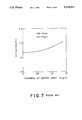
- the ratio of ⁇ f ⁇ L to V ⁇ L ( ⁇ f/V ⁇ ) represents a modulation index, and it is desirable that this value be high.
- ⁇ f/V ⁇ tends to increase with an increase of the thickness D of the buffer layer 3, but a marked improvement in optical modulation efficiency can not be expected.
- the thickness of the buffer layer 3 when the thickness of the buffer layer 3 is increased, the value of the characteristic impedance Z o tends to increase, so that it is difficult to achieve matching with an external circuit. Therefore, in view of the impedance matching with the external circuit, if Z o is determined to be about 50 ⁇ 10 ⁇ , then it is necessary that the thickness D of the buffer layer 3 be set to not more than about 1 ⁇ m.
- FIG. 8 shows an optical modulator invented by Mitomi et al. and disclosed in Japanese Patent Application Laying-Open No. 91,111/89.
- FIG. 9 shows an optical modulator proposed in the Second Optoelectronics Conference (OEC '88) Post-Deadline Papers Technical Digest, PD-1 (Oct. 1988, Tokyo).
- the thickness of traveling wave electrodes 10 and 11 (here, asymmetrical coplanar strips are used as one example) is increased in an attempt to decrease the microwave effective index n m .
- the characteristic impedance Z o is also decreased together with the microwave effective index n m .
- FIG. 9 shows a structure which improves such characteristics.
- the thickness D of the buffer layer 3 is increased to about 1 ⁇ m so as to increase the characteristic impedance Z o , thereby compensating for the reduction of Z o caused when the thickness of electrodes 10 and 11 is increased to 10 ⁇ m.
- the increase of the thickness of the buffer layer 3 also improves the value of ⁇ f/V ⁇ .
- a second object of the present invention is to provide a method of easily producing an electrically controlled optical device which is highly efficient over a wide band, which method overcomes the above difficulties heretofore involved in the manufacture of an electrically controlled optical device.
- an electrically controlled optical device comprising:
- a substrate having electro-optic effects and having at least one optical waveguide
- traveling wave electrodes provided on the buffer layer and comprising a center electrode and earth electrodes
- a shield conductor provided near to a region where the optical waveguide interacts with the traveling wave electrodes, the shield conductor confronting the traveling wave electrodes through an overlaid layer;
- the thickness of the buffer layer and the thickness of the overlaid layer being so determined that the microwave effective index of the substrate with respect to a modulating microwave signal applied to the traveling wave electrodes approaches the effective index of light propagated through the optical waveguide, and also that the characteristic impedance of the traveling wave electrodes approaches the characteristic impedance of an associated external microwave circuit.
- the thickness of the overlaid layer is 3 to 10 ⁇ m if its dielectric constant is about 1 (for example, air).
- the thickness of the buffer layer is 0.5 to 2.0 ⁇ m if its dielectric constant is not more than 4.5 (for example, silicon dioxide or Teflon).
- the thickness of the buffer layer is much increased as compared with the prior art, and the shield conductor is provided. Therefore, broad-band light modulation can be achieved without unduly increasing the driving voltage.
- the inventors of the present invention have attempted to further enhance the performance of the above electrically controlled optical device of the present invention, and have found that this electrically controlled optical device can be further improved in the following points:
- the interaction between the microwave and the light wave is less active.
- the earth electrodes are wide, the lines of electric forces from the center electrode are distributed widely over the earth electrode, and as a result the efficiency of overlapping (i.e., interaction) between the microwave and the light is about five times greater at the central electrode than at the earth electrodes. Therefore, in order to keep the driving voltage to not more than 5 V at an operating wavelength of 1.5 ⁇ m, it is necessary that the length L of interaction between the microwave and the light should be long, on the order of about 2.7 cm. Therefore, because of losses by the microwave conductor, the 3 dB modulation band is limited to 20 GHz at best.
- a material for example, a Teflon-type resin; dielectric constant ⁇ 1.9
- the buffer layer can be greatly reduced in thickness as compared with the conventional silicon dioxide layer. Therefore, when the driving voltage is designed to be the same as that of the prior art, the electrode length can be reduced, which enables the modulation band to be widened greatly. Also, when the electrode length is designed to be the same as that of the prior art, the driving voltage can be reduced greatly.
- At least those portions of the substrate disposed close to the electrodes are recessed, and at a region where light and the microwave interact with each other, part or the whole of the traveling wave electrode structure is spaced apart from that portion of the substrate disposed close to the optical waveguide, so that the microwave conductor loss is reduced, so that the effective index of the microwave conductor through the traveling wave electrode approaches the effective index of the light propagated through the optical waveguide, and so that the characteristic impedance of the traveling wave electrode approaches the characteristic impedance of the associated external circuit.
- the lines of electric force interconnecting the center electrode and the earth electrodes perceive a thick buffer layer with a low dielectric constant (for example, the dielectric constant of SiO 2 is about 4), and therefore the microwave effective index can be reduced as in the case where the buffer layer is uniformly thick.
- the depth from the interface between the air and the buffer layer to the optical waveguide can be reduced as compared with the case where the buffer layer is uniformly thick. Therefore, the efficiency of interaction between the microwave and the light becomes higher, so that the driving voltage can be reduced. As a result, the interacting length can be reduced, so that the band can be widened.
- FIG. 10 shows a velocity matching-type optical modulator proposed by Sato et al. in the Journal of Institute of Electronics and Communication Engineers of Japan (vol. J.69-C, pp. 1291-1296, 1986).
- this construction appears similar to the above construction of the present invention, but differs therefrom in that the edges of electrodes 4 and 5 which produce an electric field of high intensity are disposed in contact with a substrate 1 of a high dielectric constant (the value of this dielectric constant is approximately 35, taking the anisotropy into consideration), and in that a shield conductor is not provided. Because of these differences, the microwave effective index is not reduced sufficiently, and as a result, this conventional optical modulator suffers from the drawback that it is difficult to achieve complete velocity matching.
- FIG. 11 shows a construction proposed by Izutsu et al. in literature entitled "Picosecond Electronics and Optoelectronics" (G. A. Mourou et al. ed.), pp. 172-175, Springer-Verlag, 1985.
- this construction also appears similar to the above construction of the present invention, but differs therefrom in that the substrate is not recessed at those portions thereof disposed close to electrodes, and in that a shield conductor is not provided. Therefore, the microwave effective index can not be greatly reduced, which results in the drawback that it is difficult to achieve complete velocity matching.
- a slot is formed through at least one of the earth electrodes.
- a substrate having electro-optic effects and having at least one optical waveguide is used.
- a traveling wave electrode structure is fabricated, on a buffer layer in the vicinity of the optical waveguide, to form at least one optical control portion, thereby providing an electrically controlled optical device.
- a preformed conductor which can precisely determine the thickness of an overlaid layer is fixed in the vicinity of the electrodes of the electrically controlled optical device.
- an overlaid layer of not more than 10 ⁇ m thickness can be formed over a length of several centimeters without the need for advanced fabricating techniques, and therefore a high-speed and broad-band electrically controlled optical device of the velocity matching-type can be easily produced.
- FIG. 1A is a plan view of a conventional Mach-Zehnder light intensity (optical) modulator
- FIG. 1B is a fragmentary cross-sectional view taken along the line A--A' of FIG. 1A;
- FIG. 2A is a plan view of an optical modulator disclosed in an earlier Japanese patent application
- FIG. 2B is a fragmentary cross-sectional view taken along the line A--A' of FIG. 2A;
- FIG. 3A is a plan view of an optical modulator disclosed in an earlier Japanese patent application.
- FIG. 3B is a fragmentary cross-sectional view taken along the line A--A'of FIG. 3A;
- FIG. 6 is an illustration showing the relation between the product (V ⁇ L) of the half-wave voltage V ⁇ and the interacting length L and the thickness D of the buffer layer in the optical modulator of FIGS. 3A and 3B;
- FIG. 7 is an illustration showing the relation between the ratio ( ⁇ f/V ⁇ ) and the thickness D of the buffer layer in the optical modulator of FIGS. 3A and 3B;
- FIG. 8 is a fragmentary cross-sectional view of an optical modulator disclosed in an earlier Japanese patent application.
- FIG. 9 is a fragmentary cross-sectional view of a further conventional optical modulator.
- FIGS. 10 and 11 are cross-sectional views of further conventional optical modulators, respectively.
- FIG. 12A is a plan view of a first embodiment of the present invention.
- FIG. 12B is a fragmentary cross-sectional view taken along the line A--A' of FIG. 12A;
- FIG. 13 is an illustration showing the relation of the thickness H of an overlaid layer with a microwave effective index n m and the characteristic impedance Z o in the first embodiment
- FIG. 14 is an illustration showing the relation between the light modulation band ⁇ f ⁇ L and the thickness H of the overlaid layer in the first embodiment, in which the microwave conductor loss ⁇ is not taken into consideration;
- FIG. 15 is an illustration showing the relation between the microwave conductor loss through a traveling wave electrode structure and the thickness H of the overlaid layer in the first embodiment
- FIG. 16 is an illustration showing the relation between V ⁇ L and the thickness of the overlaid layer in the first embodiment
- FIG. 17 is an illustration showing the relation between the ratio ( ⁇ f/V ⁇ ) and the thickness H of the overlaid layer in the first embodiment
- FIG. 18A is a fragmentary cross-sectional view of a modified form of the invention, using asymmetrical coplanar strips as electrodes;
- FIG. 18B is a fragmentary cross-sectional view of another modified form of the invention, using a directional coupler as optical waveguides, thereby providing an optical modulator or an optical switch;
- FIG. 19A is a plan view of an electrically controlled optical device according to a second embodiment of the invention.
- FIG. 19B is a fragmentary cross-sectional view taken along the line A--A' of FIG. 19A;
- FIGS. 20A and 20B are illustrations showing the profile of a microwave electric field in the direction of the depth
- FIG. 21 is an illustration showing the relation between the product (V ⁇ L), of the half-wave voltage (driving voltage) and the electrode length, and the thickness of the buffer layer in the present invention
- FIG. 22 is an illustration showing calculation results of modulation bands in an electrically controlled optical device to which the present invention is applied;
- FIG. 23A is a plan view of a third embodiment of the present invention.
- FIG. 23B is a fragmentary cross-sectional view taken along the line A--A' of FIG. 23A;
- FIG. 24 is an illustration showing the relation of the depth of recessing with respect to the microwave effective index and the characteristic impedance
- FIG. 25 is an illustration showing the relation between the depth of recessing and the microwave conductor loss ⁇ ;
- FIG. 27B is a fragmentary cross-sectional view taken along the line A--A' of FIG. 27A;
- FIG. 29A is a plan view of a sixth embodiment of the present invention.
- FIG. 29B is a fragmentary cross-sectional view taken along the line A--A' of FIG. 29A;
- FIG. 30A is a plan view of a seventh embodiment of the present invention.
- FIG. 30B is a fragmentary cross-sectional view taken along the line A--A' of FIG. 30A;
- FIG. 31 is an illustration explanatory of the operation of the seventh embodiment
- FIG. 32A is a plan view of an eighth embodiment of the present invention.
- FIG. 32B is a fragmentary cross-sectional view taken along the line A--A' of FIG. 32A;
- FIGS. 33A to 33C are views showing the steps of producing an electrically controlled optical device according to a ninth embodiment of the present invention.
- FIGS. 34A to 34C are cross-sectional views of shield conductors, respectively.
- FIG. 35 is an illustration showing light-frequency response characteristics of the electrically controlled optical device of the ninth embodiment.
- FIGS. 36A to 36D are views showing the steps of producing an electrically controlled optical device according to a tenth embodiment of the present invention.
- FIG. 12A is a plan view of a first embodiment of the invention
- FIG. 12B is a fragmentary, enlarged cross-sectional view taken along the line A--A' of FIG. 12A.
- a shield conductor 9 is omitted for illustration purposes.
- a center electrode 4 and earth electrodes 5, which serve as traveling wave electrodes, are disposed above a substrate 1 of LiNbO 3 having electro-optic effects and having two optical waveguides 2.
- the shield conductor 9 is arranged through an overlaid layer 8 in the vicinity of the region where the optical waveguides 2 interact with the traveling wave electrodes 4 and 5.
- the thickness of a buffer layer 3 and the thickness of the overlaid layer 8 are determined so that the microwave effective index n m of the substrate 1 with respect to a modulating microwave signal supplied from a feeder 7 to the traveling wave electrodes 4 and 5 approaches the effective index n o of light propagated through the optical waveguides 2, and so that the characteristic impedance Z o of the traveling electrodes 4 and 5 approaches the characteristic impedance of an associated external microwave circuit.
- the width 2W of the center electrode 4 is 8 ⁇ m, and the width of the gaps 2G between the electrode 4 and the electrodes 5 is 15 ⁇ m, and the width of the optical waveguides 2 is 6 ⁇ m and hence is generally equal to the width of the center electrode 4.
- the thickness D of the buffer layer 3 of SiO 2 is 1.2 ⁇ m.
- the relation of the microwave effective index n m and the characteristic impedance Z o with the thickness H of the overlaid layer 8 is analyzed according to the analysis procedure used in FIG. 4, and the results of this analysis are shown in FIG. 13.
- n m and Z o approach to respective constant values.
- the shield conductor 9 is not provided (that is, in the case of the prior art of FIGS. 3A and 3B)
- such constant values correspond to the calculated values shown in FIG. 4.
- optical waveguides 2 can be constructed by ion exchange or by the formation of ridges, instead of Ti thermal diffusion.
- FIG. 18A Mach-Zehnder optical waveguides are used as the optical waveguides 2.
- FIG. 18B shows an optical switch employing a directional coupler in which two optical waveguides 2 are connected together and disposed close to each other.
- FIGS. 19A and 19B show a second embodiment of an electrically controlled optical device in accordance with the present invention.
- This embodiment of FIG. 19 differs from the prior art of FIGS. 1 and 2 in that the buffer layer 3 is made of a Teflon (polytetrafluoroethylene)-type resin (dielectric constant: ⁇ 1.9) instead of silicon dioxide (SiO 2 ; dielectric constant: ⁇ 3.9).
- Teflon-type resins are, for example, those (dielectric constant: ⁇ 1.9; refractive index: n ⁇ 1.3) described in Nikkei New Material, 8-7, p. 17, 1989, and the buffer layer 3 can be provided by forming such a Teflon-type material with a thickness of not more than 1 ⁇ m, using spin coating, sputtering or the like.
- FIGS. 23A and 23B show a third embodiment of the present invention in which an X-cut LiNbO 3 substrate 1 is used.
- a thick buffer layer 3 having a low dielectric constant is disposed beneath electrodes 4 and 5, and the edges of the electrodes, which generate lines of strong electric forces, are spaced apart considerably from the substrate 1. Therefore, the effect of reducing the dielectric constant is excellent.
- optical waveguides 2 are formed in the substrate 1 by an ordinary Ti thermal diffusion method. Then, while leaving those sections of the surface portion of the substrate 1 that include the optical waveguides 2, part or the whole of the remainder of the surface portion is removed by etching, so that the surface of the substrate is recessed except for protruding portions that include the optical waveguides therein.
- the effective index of the microwave and the microwave conductor loss be reduced by using a thick buffer layer, but also the driving voltage can be limited by using a thin buffer layer.
- the microwave effective index is reduced.
- FIGS. 29A and 29B show a sixth embodiment of the present invention, which differs from the fifth embodiment of FIG. 28 in that a shield conductor 9 is additionally provided, so that even if the depth of the recessing is small, a complete matching between the effective refractive indexes of the microwave and the light can be achieved.
- the driving voltage is as low as that in the fifth embodiment, the interacting length L required to obtain the desired driving voltage can be short. Therefore, the band of the light modulation can be correspondingly widened.
- a phase modulator can be provided if only the optical waveguide disposed beneath the center electrode is used in the third and fourth embodiments, or if only one of the optical waveguides is used in the fifth and sixth embodiments.
- the electrodes are constituted by a coplanar waveguide, any other suitable electrode structure such as an asymmetrical coplanar strip may be used.
- the substrate may be a Y-cut substrate of LiNbO 3 or any other suitable substrate insofar as they have electro-optic effects.
- the shield conductor is only required to serve as an electric wall, the shield conductor is not necessarily grounded to the earth electrode, and may be supported through a spacer.
- FIGS. 30A and 30B show the present invention embodied in a Mach-Zehnder light intensity modulator using a Z-cut substrate 1 of LiNbO 3 .
- a slot 12 is formed through an earth electrode 5.
- the width of a narrow conductor portion of the earth electrode is designated by 2W'.
- the center electrode 4 has a width 2W of 8 ⁇ m
- the gap 2G between the center electrode 4 and the earth electrode 5 is 15 ⁇ m
- the buffer layer 3 of SiO 2 has a thickness of 1.2 ⁇ m.
- FIG. 31 shows the value of the product (V ⁇ L) of the half-wave voltage V ⁇ and the interacting length L when 2W' is 8 ⁇ m and the width 2S of the slot 12 is a variable. As can be seen from FIG. 31, as the width 2S of the slot 12 increases, the value of the product (V ⁇ L) decreases.
- the reason for this is that the lines of electric force generated from the center electrode 4 concentrate on the narrow conductor portion (having the width 2W') of the earth electrode 5. Therefore, the driving voltage can be reduced, and the interacting length required for obtaining the desired driving voltage can be shortened. As a result, the band can be greatly widened.
- FIGS. 32A and 32B show an eighth embodiment of the present invention, which differs from the seventh embodiment of FIG. 30 in that a shield conductor 9 is additionally provided, so that the effective refractive indexes of the microwave and the light can coincide with each other, thereby achieving light modulation over quite a wide band.
- an X-cut substrate can be used instead, in which case another identical slot would also be formed through the other earth electrode, and the two optical waveguides would be disposed near the centerlines of the gaps on the opposite sides of the center electrode.
- FIGS. 33A-33C show the steps for producing an electrically controlled optical device according to the present invention.
- optical waveguides 2 are formed at the surface of a Z-cut substrate of LiNbO 3 , for example, by the Ti diffusion method. More specifically, patterns of Ti, for example, having a width of about 4 to about 9 ⁇ m and a length of 1 to 6 cm are formed, for example, by electron beam deposition and photolithography. Thereafter, the Ti is diffused into the substrate of LiNbO 3 by heat treatment to form the optical waveguides 2. Then, in FIG.
- a SiO 2 layer is formed as the buffer layer 3 on the surface of the LiNbO 3 substrate 1 having the optical waveguides 2 therein. Then, by means of vacuum deposition or the like, plating and photolithography, the center electrode 4 and earth electrodes 5 are formed on the buffer layer 3, using, for example, gold (Au), the thickness of these electrodes being, for example, 4 to 5 ⁇ m. Then, in FIG. 33C, a preformed shield conductor 9 with a groove having a depth of 0 to about 2 ⁇ m is fixed by an adhesive, thereby completing the electrically controlled optical device.
- Au gold
- FIGS. 34A-34C show examples of the shield conductor 9 having a groove for forming an overlaid layer 8.
- the groove is formed either by a wet etching technique, in which photolithography and an etchant are applied to metal, or by a dry etching technique, in which plasma or an ion beam is used.
- FIG. 34B shows a structure which is designed to overcome various stability and reliability problems caused by thermal stresses due to a difference in the thermal expansion coefficient between the substrate 1 and the shield conductor 9 and other factors.
- a metal layer of about 10 ⁇ m thickness for constituting the conductor shield 9 is formed on a support base 14, which is the same material as the substrate 1 and has the same crystalline orientation as the substrate 1. Then, the groove is formed in the metal layer according to the same procedure as in FIG. 34A.
- a groove is formed in the support base 14 either by a wet etching technique, in which photolithography and an etchant are used, or by a dry etching technique, in which plasma or an ion beam is used.
- FIG. 35 shows the light-frequency response characteristics of a light intensity modulator produced according to the same procedure described in FIGS. 33 and 34B. More specifically, this light intensity modulator was prepared according to the following procedure.
- Optical waveguides 2 were formed in a substrate 1 of LiNbO 3 by the Ti diffusion method. Then, a buffer layer 3 of SiO 2 having a thickness of 1.2 ⁇ m was formed on the substrate 1, and then a traveling wave electrode structure having a thickness of about 4.5 ⁇ m and having a center electrode 4 and earth electrodes 5 was formed on the buffer layer 3.
- the width 2W of the center electrode 4 was 8 ⁇ m, and the gap 2G was 15 ⁇ m.
- a conductor layer of gold was formed on a support base 14 of LiNbO 3 by an electron beam deposition method and plating. Then, a groove was precisely formed in the conductor layer by photolithography and the ion beam method to form the shield conductor 9. Then, the shield conductor 9 was fixed by an adhesive so as to cover the center electrode 4 and the earth electrodes 5.
- square marks indicate the light-frequency response characteristics before the shield conductor was attached, and the 3 dB band was about 8 GHz.
- 0 marks indicate the light-frequency response characteristics of the light modulator when the depth of the groove in the shield conductor was 0.5 ⁇ m, and the 3 dB band was about 18 GHz.
- ⁇ marks indicates the light-frequency response characteristics of the light modulator when the depth of the groove in the shield conductor was 0.9 ⁇ m, and the 3 dB band was about 15 GHz.
- FIGS. 36A-36D show a further modified embodiment.
- optical waveguides 2, a buffer layer 3 and traveling wave electrodes 4 and 5 were sequentially formed on a substrate 1 of LiNbO 3 .
- spacers 16 of a predetermined height for controlling the thickness of an overlaid layer 8 were formed on the electrodes 5 by photolithography and plating.
- a shield conductor 9 for example, similar to that shown in FIGS. 34A and 34B but having no groove, was fixed, thereby completing an electrically controlled optical device.
Landscapes
- Physics & Mathematics (AREA)
- Nonlinear Science (AREA)
- Electromagnetism (AREA)
- General Physics & Mathematics (AREA)
- Optics & Photonics (AREA)
- Chemical & Material Sciences (AREA)
- Engineering & Computer Science (AREA)
- Ceramic Engineering (AREA)
- Crystallography & Structural Chemistry (AREA)
- Optical Modulation, Optical Deflection, Nonlinear Optics, Optical Demodulation, Optical Logic Elements (AREA)
- Optical Integrated Circuits (AREA)
Priority Applications (1)
| Application Number | Priority Date | Filing Date | Title |
|---|---|---|---|
| US07/863,164 US5220627A (en) | 1989-02-17 | 1992-04-03 | Electrically controlled optical device |
Applications Claiming Priority (2)
| Application Number | Priority Date | Filing Date | Title |
|---|---|---|---|
| JP1-39162 | 1989-02-17 | ||
| JP3916289 | 1989-02-17 |
Related Child Applications (1)
| Application Number | Title | Priority Date | Filing Date |
|---|---|---|---|
| US07/863,164 Division US5220627A (en) | 1989-02-17 | 1992-04-03 | Electrically controlled optical device |
Publications (1)
| Publication Number | Publication Date |
|---|---|
| US5129017A true US5129017A (en) | 1992-07-07 |
Family
ID=12545429
Family Applications (2)
| Application Number | Title | Priority Date | Filing Date |
|---|---|---|---|
| US07/480,057 Expired - Lifetime US5129017A (en) | 1989-02-17 | 1990-02-14 | Electrically controlled optical device |
| US07/863,164 Expired - Lifetime US5220627A (en) | 1989-02-17 | 1992-04-03 | Electrically controlled optical device |
Family Applications After (1)
| Application Number | Title | Priority Date | Filing Date |
|---|---|---|---|
| US07/863,164 Expired - Lifetime US5220627A (en) | 1989-02-17 | 1992-04-03 | Electrically controlled optical device |
Country Status (4)
| Country | Link |
|---|---|
| US (2) | US5129017A (de) |
| EP (1) | EP0388637B1 (de) |
| JP (1) | JPH02289821A (de) |
| DE (1) | DE69016068T2 (de) |
Cited By (28)
| Publication number | Priority date | Publication date | Assignee | Title |
|---|---|---|---|---|
| US5339369A (en) * | 1992-10-23 | 1994-08-16 | General Microwave Israel Corporation | High-speed external modulator |
| US5416859A (en) * | 1993-04-14 | 1995-05-16 | The United States Of America As Represented By The Secretary Of The Navy | Broadband, low drive voltage, electrooptic, intergrated optical modulator |
| US5455876A (en) * | 1992-10-23 | 1995-10-03 | General Microwave Israel Corporation | High-speed external integrated optical modulator |
| WO1996002860A1 (en) * | 1994-07-13 | 1996-02-01 | General Microwave Israel Corporation | High-speed external modulator |
| US5625284A (en) * | 1993-07-07 | 1997-04-29 | Tokin Corporation | Electric field sensor having sensor head with unbalanced electric field shield to shield branched optical waveguides against an applied electric field |
| US5748358A (en) * | 1996-06-14 | 1998-05-05 | Sumitomo Osaka Cement Co., Ltd. | Optical modulator with optical waveguide and traveling-wave type electrodes |
| US5790719A (en) * | 1995-11-28 | 1998-08-04 | Nippon Telegraph And Telephone Corporation | Optical control device |
| US6064788A (en) * | 1997-08-14 | 2000-05-16 | Lucent Technologies Inc. | Adiabatic Y-branch modulator with negligible chirp |
| US6192167B1 (en) * | 1998-07-24 | 2001-02-20 | Uniphase Telecommunications Products | Differential drive optical modulator |
| US6222966B1 (en) | 1998-12-29 | 2001-04-24 | Lucent Technologies Inc. | Adiabatic Y-branch waveguide having controllable chirp |
| US6310700B1 (en) | 2000-09-15 | 2001-10-30 | Massachusetts Institute Of Technology | Velocity matching electrode structure for electro-optic modulators |
| US20080050082A1 (en) * | 2006-08-25 | 2008-02-28 | Ngk Insulators, Ltd. | Optical functional devices |
| US20160291353A1 (en) * | 2015-04-06 | 2016-10-06 | Lumentum Operations Llc | Modulator with signal electrode enclosed by ground electrode |
| US9810964B2 (en) | 2012-04-16 | 2017-11-07 | Leica Geosystems Ag | Electro-optic modulator having identical forward and backward electro-optic response |
| CN107957629A (zh) * | 2016-10-18 | 2018-04-24 | 天津领芯科技发展有限公司 | 基于特氟龙材料缓冲层的新型宽带铌酸锂电光调制器 |
| US10001694B1 (en) * | 2014-11-13 | 2018-06-19 | Keysight Technologies, Inc. | High-frequency light modulator |
| CN108700758A (zh) * | 2016-04-01 | 2018-10-23 | 住友大阪水泥股份有限公司 | 光调制器 |
| US10502987B2 (en) | 2015-04-07 | 2019-12-10 | Lumentum Operations Llc | High bandwidth RF or microwave interconnects for optical modulators |
| CN110687692A (zh) * | 2018-07-05 | 2020-01-14 | 苏州旭创科技有限公司 | 一种光调制器 |
| CN112485931A (zh) * | 2019-09-12 | 2021-03-12 | 苏州旭创科技有限公司 | 一种电光调制器 |
| CN113467110A (zh) * | 2020-03-31 | 2021-10-01 | Tdk株式会社 | 电光器件 |
| US11226531B2 (en) * | 2017-08-24 | 2022-01-18 | Tdk Corporation | Optical modulator |
| US20220390808A1 (en) * | 2021-05-25 | 2022-12-08 | Keysight Technologies, Inc. | Radio frequency (rf) phase velocity tuner for setting an electrooptic (eo) modulator bandwidth at different optical wavelengths |
| US11573476B2 (en) | 2017-03-03 | 2023-02-07 | Neophotonics Corporation | High frequency optical modulator with laterally displaced conduction plane relative to modulating electrodes |
| US11947147B2 (en) | 2021-03-30 | 2024-04-02 | Tdk Corporation | Optical device with microcrack resistance from surface roughness thereby reducing loss of light |
| US12265257B2 (en) | 2021-03-30 | 2025-04-01 | Tdk Corporation | Optical modulator |
| US12292627B2 (en) | 2021-03-30 | 2025-05-06 | Tdk Corporation | Optical device |
| US12386212B2 (en) | 2021-03-30 | 2025-08-12 | Tdk Corporation | Electro-optical device including optical waveguide with slope change point |
Families Citing this family (17)
| Publication number | Priority date | Publication date | Assignee | Title |
|---|---|---|---|---|
| JP2728150B2 (ja) * | 1991-03-18 | 1998-03-18 | 日本電信電話株式会社 | 光変調素子 |
| SE500991C2 (sv) * | 1992-08-17 | 1994-10-17 | Ericsson Telefon Ab L M | Anordning för anpassning av hastigheten för optiska och elektriska signaler i en vågutbredningsstruktur samt dess användning i fiberoptiska system |
| US5548668A (en) * | 1994-10-25 | 1996-08-20 | Hughes Aircraft Company | Velocity-matched electrodes for electro-optic travelling-wave modulators and method for forming the same |
| JP3723333B2 (ja) * | 1997-09-29 | 2005-12-07 | 日本碍子株式会社 | 光変調器 |
| US6372284B1 (en) * | 1998-06-11 | 2002-04-16 | Optelecom, Inc. | Fluoropolymer coating of lithium niobate integrated optical devices |
| US6522792B1 (en) * | 1998-08-10 | 2003-02-18 | Sumitomo Osaka Cement Co., Ltd. | Light modulator of waveguide type |
| US6763151B1 (en) * | 1999-07-02 | 2004-07-13 | Avanex Corporation | Electro-optic modulators with internal impedance matching |
| US6668106B1 (en) * | 2000-02-25 | 2003-12-23 | Teraburst Networks, Inc. | Crosspoint microwave switching architecture for optical telecommunications |
| CA2341052A1 (en) * | 2001-03-15 | 2002-09-15 | Tellamon Photonic Networks Inc. | Electro-optic waveguide devices |
| US20020154843A1 (en) * | 2001-04-19 | 2002-10-24 | Betts Gary E. | Dielectric backfill for optical modulators using ridged substrates |
| US7009750B1 (en) | 2002-10-25 | 2006-03-07 | Eclipse Energy Systems, Inc. | Apparatus and methods for modulating refractive index |
| US7016555B2 (en) * | 2003-03-19 | 2006-03-21 | Optimer Photonics, Inc. | Electrooptic modulators and waveguide devices incorporating the same |
| JP6375836B2 (ja) * | 2014-09-30 | 2018-08-22 | 住友大阪セメント株式会社 | 光導波路素子 |
| JP6394244B2 (ja) * | 2014-09-30 | 2018-09-26 | 住友大阪セメント株式会社 | 光制御素子 |
| JP6352789B2 (ja) * | 2014-12-09 | 2018-07-04 | 日本電信電話株式会社 | 伝送媒体および光送信器 |
| CN111065254B (zh) * | 2019-12-27 | 2022-02-15 | 武汉邮电科学研究院有限公司 | 一种带有三维屏蔽层的低损耗差分电极 |
| US11644696B2 (en) * | 2021-04-06 | 2023-05-09 | Globalfoundries U.S. Inc. | Slotted shields for use with an electro-optical phase shifter |
Citations (8)
| Publication number | Priority date | Publication date | Assignee | Title |
|---|---|---|---|---|
| EP0233797A1 (de) * | 1986-01-16 | 1987-08-26 | ETAT FRANCAIS représenté par le Ministre des PTT (Centre National d'Etudes des Télécommunications) | Elektrooptischer Richtungskoppler mit fortschreitenden Wellen und alternierender Phasenverschiebung |
| US4709978A (en) * | 1986-02-21 | 1987-12-01 | Bell Communications Research, Inc. | Mach-Zehnder integrated optical modulator |
| JPS6448021A (en) * | 1987-08-19 | 1989-02-22 | Nippon Telegraph & Telephone | Optical device |
| JPS6491111A (en) * | 1987-10-02 | 1989-04-10 | Nippon Telegraph & Telephone | High-speed optical modulator |
| US4850667A (en) * | 1987-04-14 | 1989-07-25 | Telefonaktiebolaget L M Ericsson | Electrode arrangement for optoelectronic devices |
| US4866406A (en) * | 1986-08-20 | 1989-09-12 | Sumitomo Special Metal Co., Ltd. | Wide-band optical modulator |
| JPH024020A (ja) * | 1988-06-20 | 1990-01-09 | Fujitsu Ltd | マイクロ波帯シンセサイザ |
| JPH0251123A (ja) * | 1988-08-12 | 1990-02-21 | Nippon Telegr & Teleph Corp <Ntt> | 光変調器 |
Family Cites Families (3)
| Publication number | Priority date | Publication date | Assignee | Title |
|---|---|---|---|---|
| US3923376A (en) * | 1974-08-02 | 1975-12-02 | Us Navy | Electro-optic waveguide beam deflector |
| JPS63261220A (ja) * | 1987-04-20 | 1988-10-27 | Fujitsu Ltd | 光変調素子 |
| FR2652916B1 (fr) * | 1989-10-06 | 1993-10-08 | Etat Francais Cnet | Composant polyvalent d'optique integree et reseau de distribution avec amplification optique. |
-
1990
- 1990-02-13 JP JP2029441A patent/JPH02289821A/ja active Pending
- 1990-02-14 US US07/480,057 patent/US5129017A/en not_active Expired - Lifetime
- 1990-02-16 DE DE69016068T patent/DE69016068T2/de not_active Expired - Lifetime
- 1990-02-16 EP EP90103043A patent/EP0388637B1/de not_active Expired - Lifetime
-
1992
- 1992-04-03 US US07/863,164 patent/US5220627A/en not_active Expired - Lifetime
Patent Citations (8)
| Publication number | Priority date | Publication date | Assignee | Title |
|---|---|---|---|---|
| EP0233797A1 (de) * | 1986-01-16 | 1987-08-26 | ETAT FRANCAIS représenté par le Ministre des PTT (Centre National d'Etudes des Télécommunications) | Elektrooptischer Richtungskoppler mit fortschreitenden Wellen und alternierender Phasenverschiebung |
| US4709978A (en) * | 1986-02-21 | 1987-12-01 | Bell Communications Research, Inc. | Mach-Zehnder integrated optical modulator |
| US4866406A (en) * | 1986-08-20 | 1989-09-12 | Sumitomo Special Metal Co., Ltd. | Wide-band optical modulator |
| US4850667A (en) * | 1987-04-14 | 1989-07-25 | Telefonaktiebolaget L M Ericsson | Electrode arrangement for optoelectronic devices |
| JPS6448021A (en) * | 1987-08-19 | 1989-02-22 | Nippon Telegraph & Telephone | Optical device |
| JPS6491111A (en) * | 1987-10-02 | 1989-04-10 | Nippon Telegraph & Telephone | High-speed optical modulator |
| JPH024020A (ja) * | 1988-06-20 | 1990-01-09 | Fujitsu Ltd | マイクロ波帯シンセサイザ |
| JPH0251123A (ja) * | 1988-08-12 | 1990-02-21 | Nippon Telegr & Teleph Corp <Ntt> | 光変調器 |
Non-Patent Citations (16)
| Title |
|---|
| "12 GHz -Bandwidth Ti:LiNbO3 Mach Zehnder Modulator" Seino et al., Second Optoelectronics Conf. Oct. 1988, Tokyo "Optical Subpicosecond Gate" Marcatile, Applied Optics vol. 19, No. 9, May 1st 1980, pp. 1468-1476. |
| "Picosecond Electronics and Optoelectronics", Proceedings of the Topical Meeting, Lake Tahoe, Nevada, Mar. 13-15, 1985 Ed-Mourou et al. pp. 172-175. |
| 12 GH z Bandwidth Ti:LiNbO 3 Mach Zehnder Modulator Seino et al., Second Optoelectronics Conf. Oct. 1988, Tokyo Optical Subpicosecond Gate Marcatile, Applied Optics vol. 19, No. 9, May 1st 1980, pp. 1468 1476. * |
| Applied Physics Letter, vol. 45, No. 11, Dec. 1, 1984 Becker "Traveling-Wave Electro-Optic Modulator with Maximum Bandwith-Length Product", pp. 1168-1170. |
| Applied Physics Letter, vol. 45, No. 11, Dec. 1, 1984 Becker Traveling Wave Electro Optic Modulator with Maximum Bandwith Length Product , pp. 1168 1170. * |
| Izutsu et al., "Broad-Band Guided-Wave Light Intensity Modulator," Journal of Institute of Electronics and Communication Engineers of Japan, (C) J64-C, 4 (1981), pp. 264-271. |
| Izutsu et al., Broad Band Guided Wave Light Intensity Modulator, Journal of Institute of Electronics and Communication Engineers of Japan, (C) J64 C, 4 (1981), pp. 264 271. * |
| K. Kawano, "Hybrid-Mode Analysis of a Broadside-Coupled Microstrip Line," IEE Proc. Pt. H, vol. 131 (1984), pp. 21-24. |
| K. Kawano, Hybrid Mode Analysis of a Broadside Coupled Microstrip Line, IEE Proc. Pt. H, vol. 131 (1984), pp. 21 24. * |
| K. Lizuka, "Engineering Optics" (1983), pp. 416-417 and p. 455. |
| K. Lizuka, Engineering Optics (1983), pp. 416 417 and p. 455. * |
| Kawano et al., "New Travelling-Wave Electrode Mach-Zehnder Optical Modulator with 20 GHz Bandwidth and 4.7v Driving Voltage at 1.52 μm Wavelength," Electronic Letters (Sep. 28, 1989), pp. 1382-1383. |
| Kawano et al., New Travelling Wave Electrode Mach Zehnder Optical Modulator with 20 GHz Bandwidth and 4.7v Driving Voltage at 1.52 m Wavelength, Electronic Letters (Sep. 28, 1989), pp. 1382 1383. * |
| Picosecond Electronics and Optoelectronics , Proceedings of the Topical Meeting, Lake Tahoe, Nevada, Mar. 13 15, 1985 Ed Mourou et al. pp. 172 175. * |
| Sanagi et al., "Quasi-Matched-Velocity Traveling-Wave Type Electrodes for Light Modulators and Its Analysis," Journal of Institute of Electronics and Communication Engineers of Japan, vol. J69-C (1986), pp. 1291-1296. |
| Sanagi et al., Quasi Matched Velocity Traveling Wave Type Electrodes for Light Modulators and Its Analysis, Journal of Institute of Electronics and Communication Engineers of Japan, vol. J69 C (1986), pp. 1291 1296. * |
Cited By (44)
| Publication number | Priority date | Publication date | Assignee | Title |
|---|---|---|---|---|
| US5339369A (en) * | 1992-10-23 | 1994-08-16 | General Microwave Israel Corporation | High-speed external modulator |
| US5455876A (en) * | 1992-10-23 | 1995-10-03 | General Microwave Israel Corporation | High-speed external integrated optical modulator |
| US5416859A (en) * | 1993-04-14 | 1995-05-16 | The United States Of America As Represented By The Secretary Of The Navy | Broadband, low drive voltage, electrooptic, intergrated optical modulator |
| US5625284A (en) * | 1993-07-07 | 1997-04-29 | Tokin Corporation | Electric field sensor having sensor head with unbalanced electric field shield to shield branched optical waveguides against an applied electric field |
| US5850140A (en) * | 1993-07-07 | 1998-12-15 | Tokin Corporation | Electric field sensor having sensor head with unbalanced electric field shield to shield branched optical waveguides against an applied electric field |
| WO1996002860A1 (en) * | 1994-07-13 | 1996-02-01 | General Microwave Israel Corporation | High-speed external modulator |
| US5790719A (en) * | 1995-11-28 | 1998-08-04 | Nippon Telegraph And Telephone Corporation | Optical control device |
| US5748358A (en) * | 1996-06-14 | 1998-05-05 | Sumitomo Osaka Cement Co., Ltd. | Optical modulator with optical waveguide and traveling-wave type electrodes |
| US6064788A (en) * | 1997-08-14 | 2000-05-16 | Lucent Technologies Inc. | Adiabatic Y-branch modulator with negligible chirp |
| US6192167B1 (en) * | 1998-07-24 | 2001-02-20 | Uniphase Telecommunications Products | Differential drive optical modulator |
| US6222966B1 (en) | 1998-12-29 | 2001-04-24 | Lucent Technologies Inc. | Adiabatic Y-branch waveguide having controllable chirp |
| US6310700B1 (en) | 2000-09-15 | 2001-10-30 | Massachusetts Institute Of Technology | Velocity matching electrode structure for electro-optic modulators |
| US20080050082A1 (en) * | 2006-08-25 | 2008-02-28 | Ngk Insulators, Ltd. | Optical functional devices |
| US7532777B2 (en) * | 2006-08-25 | 2009-05-12 | Ngk Insulators, Ltd. | Optical functional devices |
| US9810964B2 (en) | 2012-04-16 | 2017-11-07 | Leica Geosystems Ag | Electro-optic modulator having identical forward and backward electro-optic response |
| US10001694B1 (en) * | 2014-11-13 | 2018-06-19 | Keysight Technologies, Inc. | High-frequency light modulator |
| US10295844B2 (en) * | 2015-04-06 | 2019-05-21 | Lumentum Operations Llc | Electrode structures for optical modulators |
| US10371968B2 (en) * | 2015-04-06 | 2019-08-06 | Lumentum Operations Llc | Modulator with signal electrode enclosed by ground electrode |
| US9964784B2 (en) * | 2015-04-06 | 2018-05-08 | Lumentum Operations Llc | Modulator with signal electrode enclosed by ground electrode |
| US20160291352A1 (en) * | 2015-04-06 | 2016-10-06 | Lumentum Operations Llc | Electrode structures for optical modulators |
| US20180252948A1 (en) * | 2015-04-06 | 2018-09-06 | Lumentum Operations Llc | Modulator with signal electrode enclosed by ground electrode |
| US20160291353A1 (en) * | 2015-04-06 | 2016-10-06 | Lumentum Operations Llc | Modulator with signal electrode enclosed by ground electrode |
| US10502987B2 (en) | 2015-04-07 | 2019-12-10 | Lumentum Operations Llc | High bandwidth RF or microwave interconnects for optical modulators |
| CN108700758A (zh) * | 2016-04-01 | 2018-10-23 | 住友大阪水泥股份有限公司 | 光调制器 |
| CN108700758B (zh) * | 2016-04-01 | 2019-08-09 | 住友大阪水泥股份有限公司 | 光调制器 |
| US10935821B2 (en) * | 2016-04-01 | 2021-03-02 | Sumitomo Osaka Cement Co., Ltd. | Optical modulator |
| CN107957629A (zh) * | 2016-10-18 | 2018-04-24 | 天津领芯科技发展有限公司 | 基于特氟龙材料缓冲层的新型宽带铌酸锂电光调制器 |
| US12164210B2 (en) | 2017-03-03 | 2024-12-10 | Neophotonics Corporation | High frequency optical modulator with laterally displaced conduction plane relative to modulating electrodes |
| US11573476B2 (en) | 2017-03-03 | 2023-02-07 | Neophotonics Corporation | High frequency optical modulator with laterally displaced conduction plane relative to modulating electrodes |
| US11226531B2 (en) * | 2017-08-24 | 2022-01-18 | Tdk Corporation | Optical modulator |
| CN110687692A (zh) * | 2018-07-05 | 2020-01-14 | 苏州旭创科技有限公司 | 一种光调制器 |
| US10739664B2 (en) * | 2018-07-05 | 2020-08-11 | Innolight Technology (Suzhou) Ltd. | Optical modulator |
| CN112485931A (zh) * | 2019-09-12 | 2021-03-12 | 苏州旭创科技有限公司 | 一种电光调制器 |
| CN112485931B (zh) * | 2019-09-12 | 2023-04-21 | 苏州旭创科技有限公司 | 一种电光调制器 |
| WO2021201132A1 (en) * | 2020-03-31 | 2021-10-07 | Tdk Corporation | Electro-optical device |
| US20230124507A1 (en) * | 2020-03-31 | 2023-04-20 | Tdk Corporation | Electro-optical device |
| JP2023522151A (ja) * | 2020-03-31 | 2023-05-29 | Tdk株式会社 | 電気光学デバイス |
| CN113467110A (zh) * | 2020-03-31 | 2021-10-01 | Tdk株式会社 | 电光器件 |
| US11947147B2 (en) | 2021-03-30 | 2024-04-02 | Tdk Corporation | Optical device with microcrack resistance from surface roughness thereby reducing loss of light |
| US12265257B2 (en) | 2021-03-30 | 2025-04-01 | Tdk Corporation | Optical modulator |
| US12292627B2 (en) | 2021-03-30 | 2025-05-06 | Tdk Corporation | Optical device |
| US12386212B2 (en) | 2021-03-30 | 2025-08-12 | Tdk Corporation | Electro-optical device including optical waveguide with slope change point |
| US20220390808A1 (en) * | 2021-05-25 | 2022-12-08 | Keysight Technologies, Inc. | Radio frequency (rf) phase velocity tuner for setting an electrooptic (eo) modulator bandwidth at different optical wavelengths |
| US12124150B2 (en) * | 2021-05-25 | 2024-10-22 | Keysight Technologies, Inc. | Radio frequency (RF) phase velocity tuner for setting an electrooptic (EO) modulator bandwidth at different optical wavelengths |
Also Published As
| Publication number | Publication date |
|---|---|
| DE69016068D1 (de) | 1995-03-02 |
| DE69016068T2 (de) | 1995-05-24 |
| US5220627A (en) | 1993-06-15 |
| EP0388637A1 (de) | 1990-09-26 |
| JPH02289821A (ja) | 1990-11-29 |
| EP0388637B1 (de) | 1995-01-18 |
Similar Documents
| Publication | Publication Date | Title |
|---|---|---|
| US5129017A (en) | Electrically controlled optical device | |
| US5790719A (en) | Optical control device | |
| US5005932A (en) | Electro-optic modulator | |
| US5455876A (en) | High-speed external integrated optical modulator | |
| US5138480A (en) | Traveling wave optical modulator | |
| US6867901B2 (en) | Optical modulator and design method therefor | |
| US5416859A (en) | Broadband, low drive voltage, electrooptic, intergrated optical modulator | |
| US5339369A (en) | High-speed external modulator | |
| US5563965A (en) | Optical waveguide device with additional electrode structure | |
| JP2728150B2 (ja) | 光変調素子 | |
| JPH1039266A (ja) | 光制御デバイス | |
| JPH1090638A (ja) | 光制御素子 | |
| US5050948A (en) | Traveling wave electro-optic modulator | |
| JP2612948B2 (ja) | 光変調素子 | |
| US20030016896A1 (en) | Electro-optic waveguide devices | |
| US5647029A (en) | Traveling wave quantum well waveguide modulators using velocity matching for improved frequency performance | |
| US7088874B2 (en) | Electro-optic devices, including modulators and switches | |
| US6891982B2 (en) | Optical modulation device having excellent electric characteristics by effectively restricting heat drift | |
| JPS60114821A (ja) | 集積光デバイス | |
| JP2006317550A (ja) | 光変調器 | |
| US8170381B2 (en) | Optical modulator | |
| JPH05264937A (ja) | 光制御デバイス | |
| KR20040017535A (ko) | 저 유전율 기판을 이용한 저전압 광 변조기 | |
| JPH11316359A (ja) | 光制御デバイス | |
| JPH03229213A (ja) | 光制御素子 |
Legal Events
| Date | Code | Title | Description |
|---|---|---|---|
| AS | Assignment |
Owner name: NIPPON TELEGRAPH AND TELEPHONE CORPORATION, JAPAN Free format text: ASSIGNMENT OF ASSIGNORS INTEREST.;ASSIGNORS:KAWANO, KENJI;NOZAWA, TOSHINORI;JUMONJI, HIROMICHI;AND OTHERS;REEL/FRAME:005346/0900 Effective date: 19900410 |
|
| STCF | Information on status: patent grant |
Free format text: PATENTED CASE |
|
| CC | Certificate of correction | ||
| FEPP | Fee payment procedure |
Free format text: PAYOR NUMBER ASSIGNED (ORIGINAL EVENT CODE: ASPN); ENTITY STATUS OF PATENT OWNER: LARGE ENTITY |
|
| FPAY | Fee payment |
Year of fee payment: 4 |
|
| AS | Assignment |
Owner name: NIPPON TELEGRAPH AND TELEPHONE CORPORATION, JAPAN Free format text: CERTIFICATE EXTRACT OF REGISTER (ADDRESS CHANGE) AND SWORN ENGLISH TRANSLATION;ASSIGNOR:NIPPON TELEGRAPH AND TELEPHONE CORPORATION;REEL/FRAME:007986/0985 Effective date: 19950922 |
|
| FEPP | Fee payment procedure |
Free format text: PAYER NUMBER DE-ASSIGNED (ORIGINAL EVENT CODE: RMPN); ENTITY STATUS OF PATENT OWNER: LARGE ENTITY |
|
| FPAY | Fee payment |
Year of fee payment: 8 |
|
| FPAY | Fee payment |
Year of fee payment: 12 |