US4970435A - Plasma processing apparatus - Google Patents
Plasma processing apparatus Download PDFInfo
- Publication number
- US4970435A US4970435A US07/281,349 US28134988A US4970435A US 4970435 A US4970435 A US 4970435A US 28134988 A US28134988 A US 28134988A US 4970435 A US4970435 A US 4970435A
- Authority
- US
- United States
- Prior art keywords
- microwave
- plasma
- chamber
- waveguide
- susceptor
- Prior art date
- Legal status (The legal status is an assumption and is not a legal conclusion. Google has not performed a legal analysis and makes no representation as to the accuracy of the status listed.)
- Expired - Lifetime
Links
Images


Classifications
-
- H—ELECTRICITY
- H05—ELECTRIC TECHNIQUES NOT OTHERWISE PROVIDED FOR
- H05H—PLASMA TECHNIQUE; PRODUCTION OF ACCELERATED ELECTRICALLY-CHARGED PARTICLES OR OF NEUTRONS; PRODUCTION OR ACCELERATION OF NEUTRAL MOLECULAR OR ATOMIC BEAMS
- H05H1/00—Generating plasma; Handling plasma
- H05H1/02—Arrangements for confining plasma by electric or magnetic fields; Arrangements for heating plasma
-
- H—ELECTRICITY
- H01—ELECTRIC ELEMENTS
- H01J—ELECTRIC DISCHARGE TUBES OR DISCHARGE LAMPS
- H01J37/00—Discharge tubes with provision for introducing objects or material to be exposed to the discharge, e.g. for the purpose of examination or processing thereof
- H01J37/32—Gas-filled discharge tubes
- H01J37/32009—Arrangements for generation of plasma specially adapted for examination or treatment of objects, e.g. plasma sources
- H01J37/32357—Generation remote from the workpiece, e.g. down-stream
Definitions
- the present invention relates to a plasma processing apparatus for generating a plasma by an electron cyclotron resonance (ECR) phenomenon and, more particularly, to a plasma processing apparatus suitably used as a semiconductor manufacturing apparatus such as an ECR etching apparatus or an ECR-CVD (ECR-Chemical Vapor Deposition) apparatus.
- ECR electron cyclotron resonance
- Japanese Journal of Applied Physics Vol. 19, No. 5, May 1980, pp. 839-843 discloses a technique on reduction of metal oxides by ECR plasma of hydrogen (a model study on discharge cleaning).
- thick layers ⁇ 0.1 ⁇ m) of oxides of Cu, Ni, Fe, Mo and Ti which have widely different binding energies (metal-oxygen) are reduced by an ECR plasma. Roughly speaking, the reduction rate decreases with an increase in binding energy.
- the reduction efficiency for Cu 2 O is 0.8 initially and 0.4 on average. Concerning the other oxides, 10 -3 ⁇ 10 -2 .
- Japanese Journal of Applied Physics Vol. 21, No. 1, Jan. 1982, pp. 14-16 discloses a technique on reactive ion beam etching using a broad beam ECR in source.
- a broad-beam ion source using microwave electron cyclotron resonance (ECR) discharge has been newly developed for reactive ion beam etching, ensuring high reliability in operation.
- Ion extration characteristics comparable to those of a Kaufman-type ion source are stably obtained for various reactive gases.
- the etching characteristics of various materials such as SiO 2 and Al were investigated by introducing gases such as C 4 F 8 and SiCl 4 into the ion source. Reactive ion beam etching using the broad-beam ECR ion source is very useful for high-accuracy pattern formation.
- Japanese Journal of Applied Physics Vol. 22, No. 4, April 1983, pp. L210-L212 discloses a technique on low temperature chemical vapor deposition method utilizing an ECR plasma.
- the plasma deposition apparatus used in this technique can realize a deposition of dense and high quality thin films, such as Si 3 N 4 and SiO 2 , without the need for substrate heating.
- the deposition reactions are enhanced by using a microwave ECR plasma excitation at low gas pressures of 10 -4 Torr, and a plasma extraction by a divergent magnetic field method, which bring about highly activated plasma and ion acceleration with moderate energies of 10 to 20 eV, respectively.
- the Si 3 N 4 and SiO 2 films deposited are comparable to those prepared respectively by high temperature CVD and thermal oxidation, in evaluations such as by buffered HF solution etch rate measurement.
- the ECR plasma deposition method can be applied not only to silicon LSI, but also to compound semiconductor device fabrication processes.
- an object of the present invention to provide a plasma processing apparatus having a large-diameter plasma source capable of minimizing a reflected wave and solving problems resulting from the reflected wave.
- the present invention is a plasma processing apparatus in which a microwave is radiated on a reaction gas supplied into a plasma generating chamber to generate plasma, and predetermined processing is performed for an object placed in the reaction chamber for plasma processings, wherein the plasma generating chamber opposed to the reaction chamber has a first side face which is entirely open and faces a plane in which the object is placed, and a second side face which is located opposite to the first side face and from which the microwave is supplied, and wherein the distance between the first and second side faces is set to be an integer multiple of a 1/2wavelength of the microwave.
- a magnetic field is applied to a vacuum vessel, and a microwave in a direction perpendicular to the direction of the magnetic field is oscillated from a microwave oscillator to act on the magnetic field through a waveguide, thereby generating a plasma in the plasma generating chamber by an electron cyclotron resonance phenomenon.
- a current flowing through a susceptor on which the object to be processed is mounted may be detected, and a tuner located between a microwave supply system and a plasma generating system may be tuned to maximize the susceptor current.
- the present invention comprises a tuner located in a microwave transmission path between a microwave generating unit and the vaccum vessel, a current detecting means for applying a bias voltage to a susceptor of the vacuum vessel and detecting a current flowing through the susceptor, and a control means for tuning the tuner to maximize the detected susceptor current, and it is preferable to automatically match the vacuum vessel with the microwave transmission path.
- a wavelength adjusting means for a microwave may be connected to the waveguide immediately before the discharge chamber.
- the microwave oscillator may be connected to the vacuum vessel through a tapered waveguide.
- the reaction chamber may comprise a reaction gas supply tube having at least two gas injection tubes for injecting a reaction gas to different portions, the gas injection tubes being partially located near an installation position of the object to be processed.
- a resonance adjusting means for varying and adjusting a transmission path length of a microwave to set a resonant state may be installed to a microwave transmitting means for transmitting a microwave generated by a microwave generating source to the plasma generating chamber.
- FIG. 1 is a schematic view showing an arrangement of a plasma processing apparatus according to Embodiment 1;
- FIG. 2 is a schematic view showing positions in a vacuum vessel at which a magnetic field of 875 Gauss is generated
- FIGS. 3 and 4 are graphs showing a relationship between the 875-Gauss magnetic field generation positions in the vacuum vessel, a reflected wave generation rate and etching uniformity;
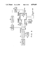
- FIG. 5 is a schematic view showing a plasma processing apparatus according to Embodiment 2.
- FIG. 6 is graph showing a relationship between a current flowing through a susceptor of the apparatus shown in FIG. 5 and a reflected power
- FIGS. 7 and 8 are circuit diagrams showing a current detector shown in FIG. 5;
- FIG. 9 is a block diagram showing a controller and a tuner driver shown in FIG. 5;
- FIG. 10 is a flow chart for explaining an operation of a one-chip CPU shown in FIG. 9;
- FIG. 11 is a perspective view showing an outer appearance of a tuner
- FIG. 12 is schematic view showing a plasma processing apparatus according to Embodiment 3.
- FIG. 13 is a graph showing data of microwave power and a reflected wave obtained when Embodiment 3 is used;
- FIG. 14 is a graph showing data of magnetic field generation conditions and a reflected wave obtained when Embodiment 3 is used;
- FIG. 15 is a schematic view showing still another embodiment different from Embodiment 3.
- FIG. 16 is a schematic view showing a plasma processing apparatus according to Embodiment 4.
- FIG. 17 is a perspective view showing a rectangular waveguide and a tapered waveguide in Embodiment 4.
- FIG. 18 is a schematic view showing an electric field distribution of a microwave in the tapered waveguide
- FIG. 19 is a sectional view showing still another embodiment different from Embodiment 4.
- FIG. 20 is a schematic view showing a plasma processing apparatus according to Embodiment 5.
- FIGS. 21 and 22 are schematic views showing reaction gas injection tubes
- FIG. 23 is a schematic view showing a plasma processing apparatus according to still another embodiment different from Embodiment 5;
- FIG. 24 is a schematic view showing a plasma processing apparatus according to Embodiment 6.
- FIG. 25 is a schematic view showing a plasma processing apparatus according to still another embodiment different from the plasma processing apparatus of Embodiment 6.
- FIG. 1 is a schematic view showing an overall plasma processing apparatus.
- Microwave oscillator 11 is connected to plasma generating chamber 15 of vacuum vessel 14 through rectangular waveguide 12 and tapered waveguide 13.
- Vessel 14 is obtained by coaxially, integrally forming cylindrical plasma generating chamber 15 and cylindrical reaction chamber 16 having a larger diameter than that of generating chamber 15.
- Generating chamber 15 is connected to reaction chamber 16 so that its side walls are located inside chamber 16.
- Generating chamber 15 is a cylindrical member having an area three to five times that of a large-diameter opening end of waveguide 13. For example, if the opening diameter of waveguide 13 is 110 mm, the diameter of vessel 14 is about 200 to 250 mm.
- Connection hole 15c having crystal plate 17 is formed in the central portion of end portion (waveguide connection end) 15a of generating chamber 15 to be connected to waveguide 13. A portion other than the central portion is closed by a wall. The end face of end portion (reaction chamber connection end) 15b of generating chamber 15 connected to reaction chamber 16 is entirely opened.
- An axial length of generating chamber 15, i.e., length l between waveguide connection end 15a and reaction chamber connection end 15b is set to be an integer multiple of a 1/2 wavelength of a microwave. Therefore, the microwave can be easily and efficiently reflected and converted into a plasma energy. For this reason, the microwave is converted into a plasma at a high ratio and rarely remains as a useless reflected wave.
- Magnetic field coil 19 surrounds generating chamber 15 of vessel 14.
- Exhaust pump 20 and gas supply unit 21 are connected to vessel 14.
- Susceptor 22 is located in reaction chamber 16 of vessel 14.
- etching or CVD is performed on semiconductor wafer A using the plasma processing apparatus having the above arrangement.
- Wafer A is placed in reaction chamber 16 of vessel 14 and held by susceptor 22.
- Entire vessel 14 is evacuated by pump 20 to about 10 -7 Torr, and a processing gas such as SF6 gas is supplied from supply unit 21 to vessel 14 at a pressure of about 10 -4 to 10 -2 Torr.
- a current is flowed through coil 19 to generate a magnetic field of 875 to 1,200 Gauss about the direction of a coil axis in generating chamber 15 of vessel 14.
- Oscillator 11 applies a microwave having a frequency, for example 2.45 GHz which satisfies electron cyclotron conditions to chamber 15 of vessel 14 through waveguides 12 and 13.
- the microwave is generated by oscillator as the pulses having a frequency of 50 to 200 Hz.
- This microwave as the pulses can generate a stable plasma in a wide range.
- an electron cyclotron resonance phenomenon occurs in chamber 15.
- the microwave is partially absorbed by rotating electrons to be directly converted into a plasma energy.
- the plasma generated in generating chamber 15 is supplied from entirely opened connection end 15b of chamber 15 to reaction chamber 16 and acts on wafer A placed in chamber 16 to perform etching or CVD.
- FIG. 2 shows positions X 1 , X 2 and X 3 at which a magnetic field of 875 Gauss is generated in the longitudinal direction of generating chamber 15.
- FIGS. 3 and 4 show a reflected wave of a microwave and etching uniformity of a wafer.
- FIG. 3 shows a reflected wave generation rate and etching uniformity obtained when a continuous microwave is used at each position at which an 875-Gauss magnetic flux is generated in the longitudinal direction of chamber 15.
- the graph shows the reflected wave generation rate and the etching uniformity at 875-Gauss magnetic flux generation point X 1 and those at positions before and after point X 1 .
- the reflected wave generation rate and the etching uniformity are poor at points X 2 and X 3 . For this reason, values obtained at points X 2 and X 3 fall outside the range of the graph shown in FIG. 3 and are therefore not shown in FIG. 3.
- the continuous microwave is used, as shown in FIG.
- the electric field is intense when the 875-Gauss magnetic field is generated at point X 1 because the microwave is not spread in chamber 15. Therefore, the microwave can be efficiently converted into a plasma by an interaction of the electric field and the magnetic field, and a reflected wave is less generated. In this state, however, since an intense plasma is generated in a narrow range, an etching rate of wafer A is higher at the central portion of the wafer, resulting in poor etching uniformity.
- the 875-Gauss magnetic field is generated at points X 2 and X 3 , the electric field of the microwave is wide and weak. Therefore, the microwave cannot be efficiently converted into a plasma. For this reason, a reflected wave of the microwave is increased, and plasma generation becomes unstable. Also, the etching uniformity is further degraded. Therefore, when the continuous microwave is used, wafer A cannot be uniformly etched.
- FIG. 4 shows the reflected wave generation rate and the etching uniformity obtained at each 875-Gauss generation point in the overall longitudinal direction of chamber 15 when a pulse microwave is used. As is apparent from FIG. 4, the reflected wave generation rate and the etching uniformity are good throughout the axial length of chamber 15.
- the area of chamber 15 of vessel 14 is three times that of the waveguide and connection portion 15b of chamber 15 is entirely opened. For this reason, a large-diameter plasma can act on wafer A.
- the area of chamber 15 need not be three to five times that of waveguide 13 but may be more than that. That is, the larger the area is, the less the reflected wave is generated.
- a microwave oscillator having a rated output much higher than an operation output is used.
- a microwave oscillator having a rated output of 1,500 W is used, and a maximum operation output is limited to 500 W.
- FIG. 5 the same reference numerals as in the conventional apparatus shown in FIG. 3 denote the corresponding parts and a detailed description thereof will be omitted.
- an output from microwave generator 30 is supplied to discharge chamber 38 through waveguide 32 and tuner 36, thereby generating a plasma in discharge chamber 38 and reaction chamber 40.
- FIG. 6 shows a measurement result. At this time, measurement of the reflected power was performed using a conventional apparatus given of the results shown in FIG. 3.
- current Is and the microwave reflected power have a predetermined correlation. That is, when the microwave reflected power is minimized, effective microwave power to be supplied to chambers 38 and 40 is maximized. This is because current Is flowing through susceptor 44 is maximized by ions or electrons generated by the plasma.
- current detector 62 applies a negative bias voltage to susceptor 44 and current detector 62 is connected to susceptor 44.
- Controller 58 calculates a tuning signal on the basis of detected susceptor current Is so that current Is is maximized and outputs the signal to tuner driver 60.
- Driver 60 tunes tuner 36 on the basis of the tuning signal and adjusts the length of waveguide 32 so that waveguide 32 matches with discharge chamber 38.
- tuner 36 can be automatically tuned on the basis of current (Is) flowing through susceptor 44. For this reason, as compared with a conventional technique using power monitor 34 and display unit 56, tuning control can be performed very simply.
- detector 62 of above-mentioned embodiment comprises DC bias source 64, resistor 66, capacitor 68 and amplifier 70.
- a negative bias voltage is applied to susceptor 44 by bias source 64, and a current flowing through susceptor 44 is detected through amplifier 70.
- RF bias source 72 may be used in place of DC bias source 64 as shown in FIG. 8.
- controller 58 of above-mentioned embodiment comprises a one-chip CPU.
- Current Is output from detector 62 is supplied to the one-chip CPU.
- a one-way movement end limit signal and a +- direction movement end limit signal are supplied from limit switches 74a and 74b located at tuner 36 to the CPU.
- Driver 60 of this embodiment comprises motor driver 80, motor 82 and drive mechanism 84, as shown in FIG. 16, and can adjust the length of tuner 36.
- the one-chip CPU constituting controller 58 which is mentioned above, performs calculations in accordance with a flow chart shown in FIG. 17.
- controller 58 reads current detected by detector 62 at each predetermined time interval, e.g., five seconds in this case and calculates change amount In.
- controller 58 determines that detected current (Is) is close to the maximum value and stops automatically tuner 36 at the position.
- controller 58 checks whether amount In is positive or negative. If controller 58 determines that change amount ⁇ In is a positive value, it increases the length of tuner 34 so that the value of Is is maximized. If controller 58 determines that change amount ⁇ In is negative, it decreases the length of tuner 16 so that the value of (Is) is similarly maximized.
- Controller 48 repeatedly performs the above operation at an interval of five seconds.
- the length of tuner 36 is automatically controlled to match waveguide 32 with discharge chamber 38, thereby minimizing reflected power from chamber 38.
- tuner 36 and drive mechanism 84 constitute a tuning mechanism shown in FIG. 11.
- This tuning mechanism comprises fixed waveguide 90, movable waveguide 92, fixed waveguide bracket 94, movable waveguide bracket 96, motor 82, pulleys 100 and 102, drive belts 104a and 104b, drive ball screw 106, slide bearing 08 and slide shaft 110.
- a rotational output from motor 82 is transmitted to belts 104a and 104b and then to pulleys 102 and 100.
- Screw 106 is directly connected to pulley 100. Rotation of motor 82 is therefore transmitted to screws 106 to move bracket 86, thereby automatically moving waveguide 92 to a position at which current Is is maximized.
- shaft 110 is fixed to bracket 94 to serve as a shaft of bearing 108 fixed to bracket 96.
- Such a tuning mechanism is satisfactory as long as it can automatically vary and adjust the length of waveguide 92 using a motor, an air cylinder or another drive source to perform tuning. Therefore, in place of the ball screw, a driving means such as a rack and a pinion may be used.
- tuner 36 is of a type which changes the length of a waveguide.
- the present invention is not limited to this embodiment, but a tuner of another type, e.g., a stub tuner or an EH tuner may be used. Also, two or more tuners of any of the above type may be used in a combination.
- controller 58 comprises a one-chip CPU.
- the present invention is not limited to this embodiment, but a circuit arrangement of the controller may be of either an analog or digital type.
- controller 58 adjusts the position of tuner 36 in accordance with the flow shown in FIG. 10.
- the present invention is not limited to this embodiment, but another adjusting method may be used if necessary.
- a variable range of tuner 36 may be entirely scanned to detect a position at which susceptor current Is is minimized so that the position of tuner 36 is adjusted to this position.
- reflected power of a microwave is detected on the basis of a susceptor current.
- the microwave power monitor and the like used in the conventional apparatus shown in FIG. 3 need not be used. Therefore, tuning control of the tuner can be performed using a compact and inexpensive device.
- reference numeral 201 denotes a microwave source for generating a microwave.
- This plasma processing apparatus comprises microwave source 201, waveguides 202 to 205 for transmitting a microwave, discharge chamber 206 for generating a plasma and reaction chamber 207 for performing deposition on a sample by the generated plasma.
- Small coil 208 surrounds discharge chamber 206 to generate a magnetic field.
- Microwave source 201 is a microwave generating unit such as a magnetron for generating a microwave of, e.g., an industrial frequency (2.45 GHz).
- Waveguides 202 to 205 are metal tubes made of stainless steel or the like.
- Power monitor 203a is connected to waveguide 203 to measure incident power and reflected power of a generated microwave and monitor a reflected wave.
- Waveguide 204 is an E corner for changing a transmission path of the microwave through a right angle.
- Waveguide 205 is a tapered waveguide in which dielectric plate 209 is inserted perpendicularly to a propagation direction of the microwave.
- the microwave propagating through plate 209 is converted from a TE10 mode into a quasi-TM mode.
- a crystal plate can be used as plate 209.
- Waveguide 205 is located immediately before and connected to discharge chamber 206.
- Three stubs 210 as a wavelength adjusting means for a microwave are connected to waveguide 205. That is, waveguide 205 performs mode conversion of the microwave and adjustment of the wavelength.
- Member 211 is inserted between waveguide 205 and chamber 206 to pass the microwave and seal a vacuum in chamber 206. Similar to dielectric plate 209, a crystal plate is suited as member 211.
- Chamber 206 is designed to serve as a microwave resonating chamber. Chamber 206 therefore has a length corresponding to one wavelength in a vacuum of the microwave in an electric field direction and has microwave reflecting plate 212 at its one end. Opening portion 212a is formed in plate 212 to supply a plasma generated in discharge chamber 206 to reaction chamber 207.
- the diameter of opening portion 212a may be 60 to 80 mm as in the conventional apparatus. More preferably, the diameter is set to be about 100 to 120 mm. The value may be changed in accordance with the diameter of a sample such as a wafer to be processed.
- Coil 208 is preferably a small coil having a cooling unit inside the coil, e.g., a tube coil in which cooling water is circulated in a tube to improve a cooling efficiency.
- Coil 208 generates a magnetic field perpendicular to an electric field.
- Chamber 206 has inlet port 213 for supplying a gas such as N 2 , O 2 or Ar serving as a plasma source.
- a gas such as N 2 , O 2 or Ar serving as a plasma source.
- Reaction chamber 207 utilizes the plasma generated in discharge chamber 206 to perform CVD on sample W such as a wafer substrate and includes sample table 214. Sample W is conveyed to and placed on table 214 by a convey mechanism (not shown).
- SiH 4 or the like is supplied from gas inlet port 215. In this case, if a generated plasma is an N 2 plasma, Si 3 N 4 is deposited on the sample by an interaction of the N 2 plasma and SiH 4 . If an O 2 plasma is generated, SiO 2 is deposited.
- Chambers 206 and 207 are connected to a vacuum system (not shown), and deposition is performed at a desired pressure (reduced pressure) in accordance with a purpose.
- microwave source 201 generates a continuous microwave.
- microwave source 201 can also generate a pulse of microwave.
- the microwave is supplied to waveguide 105 through waveguides 202 to 204, Converted from the TE 10 mode into a circular TE 11 mode therein, and transmitted to discharge chamber 206.
- a gas serving as a plasma source is supplied from gas inlet port 215 to chamber 206.
- a desired magnetic field is generated chamber 206 by small coil 208. Therefore, the transmitted microwave resonates in chamber 206 and an electric field energy is absorbed with high efficiency, thereby generating a highly active plasma.
- an impedance of chamber 206 changes and its length no longer corresponds to the wavelength of the microwave.
- the generated plasma flows as a plasma stream from opening portion 212a of reflecting plate 212 to reaction chamber 207.
- the plasma collides against sample W on sample table 214 by an interaction with a supplied reaction gas to perform deposition.
- a bias voltage is applied to table 214 if necessary, so that an under film portion is flattened and side wall portions are rendered dense.
- opening portion 212a is wide, the plasma stream is uniform throughout a wide range from its center, and deposition can be therefore uniformly performed.
- FIG. 13 shows data of power and a reflected wave obtained by the apparatus of this embodiment when a continuous wave is used.
- FIG. 14 shows data of a reflected wave obtained when a generation position of 875 Gauss as an ECR condition is changed by changing a coil current.
- the microwave power was 400 W or more
- the percentage of a reflected wave was stably very small at about 1%.
- the percentage of the reflected wave was very small at about 1%.
- the type or pressure of the discharge gas was changed, the same result was obtained.
- a tapered waveguide is used immediately before chamber 206, and dielectric plate 209 is inserted therein.
- the present invention is not limited to this embodiment. For example, even if the mode of the microwave is not converted or the waveguide is a circular tube, the reflected wave can be effectively minimized.
- an adjusting means for microwave matching is not limited to the three stubs but may be a waveguide with two stubs 210' shown in FIG. 15 or the like.
- a plasma CVD apparatus since matching of a microwave is performed immediately before the discharge chamber, matching can be performed with a good response characteristic, and a reflected wave of the microwave can be minimized.
- the diameter of a plasma stream can be increased accordingly. For this reason, etching or deposition can be uniformly performed to manufacture a high-quality product.
- the percentage of the reflected wave can be decreased to 1% or less.
- a continuous wave of microwave is generated as a output
- a plasma is not intermittently generated as when a pulse wave is used. Therefore, particles are not generated nor adhere on a sample, or a sample is not damaged by a high self bias.
- the adjusting means of the microwave is located at the waveguide immediately before the discharge chamber. For this reason, since a three-stub tuner need not be used as in the conventional apparatus, the overall apparatus can be made compact.
- FIG. 16 is a schematic view showing an arrangement of a plasma processing apparatus according to this embodiment.
- the same reference numerals as in FIG. 6 denote the same parts, and a detailed description thereof will be omitted.
- tapered waveguide 410 is inserted between rectangular waveguide 402 and generating chamber 403 of vacuum vessel 405.
- one end opening of waveguide 410 is formed into a rectangle having a size corresponding to a rectangular section of waveguide 402, and the other end thereof is formed into a circle having a size corresponding to a circular section of chamber 403.
- Waveguide 410 is tapered such that a rectangular section is gradually deformed into a circular section from rectangular opening 411 to circular opening 412, thereby gradually increasing a sectional area.
- Rectangular opening 411 of tapered waveguide 410 is connected to a rectangular opening at the end portion of rectangular waveguide 402.
- Circular opening 412 is connected to a circular opening of generating chamber 403.
- a microwave oscillated by oscillator 401 propagates through waveguide 402 and then waveguide 410.
- waveguide 410 a sectional shape of an electric field of the microwave is gradually deformed from a rectangle to a shape close to a circle in accordance with the tapered shape of waveguide 410.
- a sectional area of the electric field is gradually increased.
- FIG. 18 shows the shape of the electric field of the microwave finally obtained at circular opening 412 as an outlet of waveguide 410. In this manner, the shape of the electric field of the microwave is converted into a shape close to a circle, and the microwave is supplied into circular generating chamber 403.
- chamber 403 can generate a plasma having an electric field the shape of which is substantially similar to that of the electric field formed at the outlet of waveguide 410, i.e., an electric field close to a circle and having a large sectional area.
- This plasma can act on the entire surface of circular wafer A placed on susceptor 409 in reaction chamber 404. Therefore, etching or CVD can be uniformly performed on the entire surface of wafer A. As a result, a problem in that an unprocessed portion partially remains can be prevented.
- FIG. 19 shows still another embodiment.
- tapered waveguide 410 and plasma generating chamber 403 are integrally formed.
- Chamber 403 has height h and diameter d determined by a vacuum vessel design size.
- Chamber 403 has therein internal vessel 414 made of a material such as a crystal capable of maintaining a vacuum and transmitting a microwave and having a size close to the size of chamber 403.
- Vessel 414 is used to uniformly apply a plasma to a wafer.
- etching or CVD can be uniformly performed by the presence of vessel 414.
- a plasma can act on the entire surface of a semiconductor wafer to uniformly perform etching or CVD thereon.
- This plasma processing apparatus comprises, as a plasma generating system for generating a plasma, microwave source 501, waveguide 502, discharge chamber 503 and coil 505. Chamber 503 is connected to film formation chamber 507 as a reaction chamber for CVD film formation.
- Microwave source 501 is a device such as a magnetron for generating a microwave of, e.g., an industrial frequency (2.45 GHz).
- Waveguide 502 is a metal tube for transmitting the generated microwave and, if necessary, includes a wavelength adjusting means, a mode conversion means and a reflected wave monitor unit for the microwave.
- Gas supply tube 504 is connected to chamber 503 and supplies a gas such as N 2 , O 2 or Ar serving as a plasma source selected in accordance with the type of a film to be formed. The gas is supplied at a predetermined flow rate.
- a magnetic field in an electric field direction is generated in chamber 503 by coil 505.
- the intensity of the magnetic field satisfying ECR conditions is, e.g., 875 Gauss with respect to a microwave of 2.45 GHz.
- ECR conditions e.g. 875 Gauss with respect to a microwave of 2.45 GHz.
- the frequency of the microwave and the intensity of the magnetic field may be arbitrarily selected as long as the above effect is achieved.
- Discharge chamber 503 and film formation chamber 507 are connected to a vacuum system (not shown) and maintained at a predetermined pressure. For this reason, sealing member 512 is inserted between waveguide 502 and chamber 503 to seal a vacuum and transmit the microwave.
- Chamber 503 includes microwave reflecting plate 506 located at its end portion connected to film formation chamber 507 so that the microwave resonates in chamber 503.
- a plasma stream is supplied from opening portion 506a of plate 506 to chamber 507.
- Chamber 507 includes sample table 508, and a convey mechanism (not shown) conveys sample W onto table 508.
- Two inlet ports 509 are formed in chamber 507 to supply a reaction gas for film formation, and ring-like gas injection tubes 510A and 510B are connected to ports 509.
- each of tubes 510A and 510B consists of ring tube 510 made of a crystal and having a plurality of gas injection holes 510a.
- the diameter of tube 510A is larger than that of tube 510B.
- Tube 510A is separated from sample W and plasma stream P, while tube 510B is located near the periphery of sample W so as to be in contact with plasma stream P.
- a reaction gas of the same type is supplied to tubes 510A and 510B from a gas supply system (not shown).
- the reaction gas are silane gas (SiH 4 ), boron and phosphorus and sometimes supplied as a gas mixture with argon (Ar) or N 2 gas.
- a flow rate of the reaction gas or a mixing ratio of the gas mixture is controlled in accordance with film formation conditions.
- these parameters are controlled by tubes 510A and 510B.
- the gas supply system includes valves 511 which are automatically controlled, and film formation uniformity is measured beforehand under predetermined film formation conditions. In actual film formation, therefore, both the valves can be controlled to obtain an optimal value on the basis of the measurement result.
- a plasma of the gas supplied from supply tube 504 is generated and flowed as plasma stream P to film formation chamber 507.
- the reaction gas is injected from gas injection tubes 510A and 510B and diffused throughout the chamber.
- the reaction gas reacts with the supplied plasma to deposit a reaction product film on the surface of a sample.
- a film formation rate is in proportion to the plasma intensity and higher at the central portion of the sample.
- the reaction gas is also supplied to the vicinity of the sample from tube 510B located near the plasma and the sample. Therefore deposition is promoted at the periphery of sample W. As a result, a reaction product film is uniformly formed on the sample surface.
- the flow rate of the reaction gas supplied from tubes 510A and 510B' can be adjusted by automatically controlling valves 511 in accordance with film formation conditions.
- two large and small ring-like gas injection tubes 510A and 510B are used as a gas injection tube.
- the number, the size and the shape of the gas injection tubes are not limited to those of the above embodiment.
- the gas injection tube separated from the plasma need not be a ring but may be a straight tube or the like.
- the gas injection tube located near the sample need not be a circular ring but may be square-ring gas injection tube 510' as shown in FIG. 22 or comprise a plurality of straight tubes. That is, the gas injection tube located near the sample may take any shape as long as it can supply the reaction gas to the vicinities of the sample and the plasma or in the plasma stream.
- ring-like gas injection tube 510 having gas injection holes 510a opposing the periphery of sample W may be located near sample W and n plasma stream P, as shown in FIG. 23.
- the film formation uniformity can be significantly improved.
- a superior effect can be achieved for a large-diameter wafer.
- a plasma processing apparatus according to still another embodiment of the present invention will be described with reference to FIG. 24.
- waveguide 606 serves as a microwave transmitting means for transmitting microwave 604 generated by microwave oscillator 602 serving as a microwave generating source to discharge chamber 608 serving as a plasma generating chamber, and tuner 632 is connected to waveguide 606 to serve as a resonance adjusting means for varying the length of a transmission path of microwave 604 to obtain a resonant state.
- Tuner 632 has a double-pipe structure at a position connected to waveguide 606, thereby adjusting the transmission path length.
- microwave 604 passing through tuner 632 is supplied to discharge chamber 608 through crystal 626.
- the length of tuner 632 can be changed in correspondence with a change in permittivity of chamber 608 and in accordance with a change ratio of the wavelength of microwave 604 in chamber 608.
- microwave 604 from tuner 632 can be matched with chamber 608, thereby realizing a nonreflecting state.
- tuner 632 can correspond to the change from the vacuum to plasma state in chamber 608.
- Tuner 632 may comprise a cavity resonator connected to both waveguide 606 and discharge chamber 608 so as to be freely expanded/contracted, as shown in FIG. 25. Also in this case, the same effect can be obtained.
- the plasma processing apparatus of the present invention can be effectively used in combination with a widely-used microwave tuner such as a 603 stub tuner.
- tuning can be performed in a wide resonance range to minimize a reflected wave. Therefore, since microwave power can be effectively utilized, a microwave oscillator of a minimum necessary output can be used.
- a cost of the apparatus can be decreased. Also, since almost no reflected wave is generated, a circulator or load need not be used. As a result, the apparatus can be made compact at low cost.
Landscapes
- Physics & Mathematics (AREA)
- Engineering & Computer Science (AREA)
- Plasma & Fusion (AREA)
- Chemical & Material Sciences (AREA)
- Analytical Chemistry (AREA)
- Optics & Photonics (AREA)
- Spectroscopy & Molecular Physics (AREA)
- Drying Of Semiconductors (AREA)
- Plasma Technology (AREA)
Applications Claiming Priority (4)
| Application Number | Priority Date | Filing Date | Title |
|---|---|---|---|
| JP31120087A JPH0831445B2 (ja) | 1987-12-09 | 1987-12-09 | プラズマ処理装置 |
| JP62-311200 | 1987-12-09 | ||
| JP63127567A JPH01298170A (ja) | 1988-05-25 | 1988-05-25 | Ecrプラズマ処理装置 |
| JP63-127567 | 1988-05-25 |
Publications (1)
| Publication Number | Publication Date |
|---|---|
| US4970435A true US4970435A (en) | 1990-11-13 |
Family
ID=26463498
Family Applications (1)
| Application Number | Title | Priority Date | Filing Date |
|---|---|---|---|
| US07/281,349 Expired - Lifetime US4970435A (en) | 1987-12-09 | 1988-12-08 | Plasma processing apparatus |
Country Status (2)
| Country | Link |
|---|---|
| US (1) | US4970435A (ko) |
| KR (1) | KR960014434B1 (ko) |
Cited By (49)
| Publication number | Priority date | Publication date | Assignee | Title |
|---|---|---|---|---|
| US5063330A (en) * | 1988-05-09 | 1991-11-05 | Centre National De La Recherche Scientifique | Plasma reactor |
| US5074985A (en) * | 1989-10-06 | 1991-12-24 | Hitachi, Ltd. | Film forming apparatus |
| EP0478283A2 (en) * | 1990-09-26 | 1992-04-01 | Hitachi, Ltd. | Microwave plasma processing method and apparatus |
| US5111111A (en) * | 1990-09-27 | 1992-05-05 | Consortium For Surface Processing, Inc. | Method and apparatus for coupling a microwave source in an electron cyclotron resonance system |
| US5134965A (en) * | 1989-06-16 | 1992-08-04 | Hitachi, Ltd. | Processing apparatus and method for plasma processing |
| US5160397A (en) * | 1989-04-27 | 1992-11-03 | Fujitsu Limited and Fuji Electric Co., Ltd. | Plasma process apparatus and plasma processing method |
| US5172083A (en) * | 1991-05-14 | 1992-12-15 | Nippon Steel Corporation | Microwave plasma processing apparatus |
| US5196670A (en) * | 1989-10-03 | 1993-03-23 | University Of Cincinnati | Magnetic plasma producing device with adjustable resonance plane |
| US5280219A (en) * | 1991-05-21 | 1994-01-18 | Materials Research Corporation | Cluster tool soft etch module and ECR plasma generator therefor |
| US5302803A (en) * | 1991-12-23 | 1994-04-12 | Consortium For Surface Processing, Inc. | Apparatus and method for uniform microwave plasma processing using TE1101 modes |
| US5310426A (en) * | 1989-08-03 | 1994-05-10 | Uha Mikakuto Precision Engineering Research Institute Co., Ltd. | High-speed film forming method by microwave plasma chemical vapor deposition (CVD) under high pressure and an apparatus therefor |
| US5344536A (en) * | 1991-12-03 | 1994-09-06 | Tokyo Ohka Kogyo Co., Ltd. | Method of and apparatus for processing a workpiece in plasma |
| US5378284A (en) * | 1990-04-03 | 1995-01-03 | Leybold Aktiengesellschaft | Apparatus for coating substrates using a microwave ECR plasma source |
| EP0644575A1 (en) * | 1993-09-17 | 1995-03-22 | Hitachi, Ltd. | Plasma generating method and apparatus and plasma processing method and apparatus |
| US5451259A (en) * | 1994-02-17 | 1995-09-19 | Krogh; Ole D. | ECR plasma source for remote processing |
| US5804033A (en) * | 1990-09-26 | 1998-09-08 | Hitachi, Ltd. | Microwave plasma processing method and apparatus |
| WO1999004606A2 (en) * | 1997-07-14 | 1999-01-28 | Lam Research Corporation | Compact microwave downstream plasma system |
| US5869802A (en) * | 1995-12-21 | 1999-02-09 | Plasmaquest, Inc. | Plasma producing structure |
| US5983828A (en) * | 1995-10-13 | 1999-11-16 | Mattson Technology, Inc. | Apparatus and method for pulsed plasma processing of a semiconductor substrate |
| US6060131A (en) * | 1997-12-30 | 2000-05-09 | Shimadzu Corporation | Method of forming a thin film by plasma chemical vapor deposition |
| US6200651B1 (en) * | 1997-06-30 | 2001-03-13 | Lam Research Corporation | Method of chemical vapor deposition in a vacuum plasma processor responsive to a pulsed microwave source |
| EP1094505A1 (en) * | 1996-11-20 | 2001-04-25 | Tokyo Electron Limited | Plasma treating device |
| US6223686B1 (en) | 1998-02-06 | 2001-05-01 | Shimadzu Corporation | Apparatus for forming a thin film by plasma chemical vapor deposition |
| US6294466B1 (en) | 1998-05-01 | 2001-09-25 | Applied Materials, Inc. | HDP-CVD apparatus and process for depositing titanium films for semiconductor devices |
| US6305315B1 (en) * | 1999-03-25 | 2001-10-23 | Shimadzu Corporation | ECR plasma apparatus |
| US6313583B1 (en) * | 1998-12-01 | 2001-11-06 | Matsushita Electric Industrial Co., Ltd. | Plasma processing apparatus and method |
| US6396214B1 (en) * | 1998-12-07 | 2002-05-28 | Robert Bosch Gmbh | Device for producing a free cold plasma jet |
| US6395641B2 (en) | 1995-10-13 | 2002-05-28 | Mattson Techonolgy, Inc. | Apparatus and method for pulsed plasma processing of a semiconductor substrate |
| US20030046640A1 (en) * | 2001-08-29 | 2003-03-06 | Wheeler William R. | Generating a logic design |
| US20030141822A1 (en) * | 2002-01-31 | 2003-07-31 | Tokyo Electron Limited | Method and apparatus for determination and control of plasma state |
| EP1377138A1 (en) * | 2001-03-28 | 2004-01-02 | Tokyo Electron Limited | Device and control method for micro wave plasma processing |
| US20040084422A1 (en) * | 2002-09-18 | 2004-05-06 | Rudolf Beckmann | Plasma source |
| US20040168788A1 (en) * | 2001-07-18 | 2004-09-02 | Pavel Dvoskin | Riser(s) size reduction and/or metal quality improving in gravity casting of shaped products by moving electric arc |
| US6794301B2 (en) | 1995-10-13 | 2004-09-21 | Mattson Technology, Inc. | Pulsed plasma processing of semiconductor substrates |
| US6792889B2 (en) * | 2002-01-30 | 2004-09-21 | Alps Electric Co., Ltd. | Plasma processing apparatus and method capable of performing uniform plasma treatment by control of excitation power |
| US20050034840A1 (en) * | 2001-08-23 | 2005-02-17 | Pavel Dvoskin | Method and apparatus for stirring and treating continuous and semi continuous metal casting |
| US20050098298A1 (en) * | 2000-12-12 | 2005-05-12 | Pavel Dvoskin | Treating molten metals by moving electric arc |
| US20060065195A1 (en) * | 2002-12-20 | 2006-03-30 | Hamamatsu Foundation For Science And Technology Pr | Microwave plasma generating device |
| US20060132068A1 (en) * | 2004-12-16 | 2006-06-22 | General Electric Company | Ion source apparatus and method |
| US20060283550A1 (en) * | 2005-06-06 | 2006-12-21 | Hideyuki Kazumi | Plasma processing apparatus |
| DE102006043943A1 (de) * | 2006-09-14 | 2008-03-27 | Leybold Optics Gmbh | Verfahren zum Aufbringen von Schichten auf Substraten mit gekrümmten Oberflächen |
| US20100006227A1 (en) * | 2005-08-15 | 2010-01-14 | The Boc Group Plc | Microwave Plasma Reactor |
| US7670453B1 (en) * | 1999-04-29 | 2010-03-02 | Sidel Participations | Device for treating a container with microwave plasma |
| US20100322827A1 (en) * | 2008-02-18 | 2010-12-23 | Cs Clean Systems Ag | Method and device for cleaning the waste gases of a processing system |
| US20120186747A1 (en) * | 2011-01-26 | 2012-07-26 | Obama Shinji | Plasma processing apparatus |
| US20160157330A1 (en) * | 2013-05-27 | 2016-06-02 | Adtec Plasma Technology Co., Ltd. | Cavity Resonator of Microwave Plasma Generating Apparatus |
| US9581741B1 (en) * | 2013-05-31 | 2017-02-28 | Itn Energy Systems, Inc. | Infrared control coating of thin film devices |
| GB2593159A (en) * | 2020-03-12 | 2021-09-22 | Univ Lancaster | Method and apparatus for supplying electromagnetic power to a plasma vessel |
| CN114959631A (zh) * | 2022-04-24 | 2022-08-30 | 北京科技大学 | 一种双端馈入微波电子回旋共振等离子体化学气相沉积装置 |
Families Citing this family (2)
| Publication number | Priority date | Publication date | Assignee | Title |
|---|---|---|---|---|
| KR100976976B1 (ko) * | 2002-12-26 | 2010-08-23 | 삼성전자주식회사 | 고주파 정합장치 |
| WO2010064818A2 (ko) * | 2008-12-02 | 2010-06-10 | 트리플코어스코리아 | 상압 플라즈마 발생 장치 및 이를 이용한 상압 플라즈마 발생 방법 |
Citations (17)
| Publication number | Priority date | Publication date | Assignee | Title |
|---|---|---|---|---|
| US3828722A (en) * | 1970-05-01 | 1974-08-13 | Cogar Corp | Apparatus for producing ion-free insulating layers |
| US4201579A (en) * | 1978-06-05 | 1980-05-06 | Motorola, Inc. | Method for removing photoresist by hydrogen plasma |
| JPS5824711A (ja) * | 1981-08-05 | 1983-02-14 | Kawasaki Heavy Ind Ltd | 流動床燃焼ボイラの燃焼室構造 |
| US4401054A (en) * | 1980-05-02 | 1983-08-30 | Nippon Telegraph & Telephone Public Corporation | Plasma deposition apparatus |
| US4423303A (en) * | 1980-05-06 | 1983-12-27 | Tokyo Shibaura Denki Kabushiki Kaisha | Apparatus for treating powdery materials utilizing microwave plasma |
| JPS608622A (ja) * | 1983-06-28 | 1985-01-17 | Matsushita Electric Ind Co Ltd | 風呂の制御装置 |
| JPS6024034A (ja) * | 1984-02-20 | 1985-02-06 | Hitachi Ltd | ウエハ反転装置 |
| JPS60201641A (ja) * | 1984-03-27 | 1985-10-12 | Fujitsu Ltd | ウエハの並べ換え装置 |
| JPS61157325A (ja) * | 1984-12-28 | 1986-07-17 | Toa Nenryo Kogyo Kk | 気体選択透過膜およびその製造方法 |
| JPS61191015A (ja) * | 1985-02-20 | 1986-08-25 | Hitachi Ltd | 半導体の気相成長方法及びその装置 |
| US4611121A (en) * | 1983-04-19 | 1986-09-09 | Nihon Shinku Gijutsu Kabushiki Kaisha | Magnet apparatus |
| JPS6258630A (ja) * | 1985-09-09 | 1987-03-14 | Hitachi Ltd | プラズマ処理制御方法及び装置 |
| JPS62210621A (ja) * | 1986-03-12 | 1987-09-16 | Hitachi Ltd | マイクロ波プラズマ処理方法および装置 |
| JPS6360530A (ja) * | 1986-09-01 | 1988-03-16 | Denki Kogyo Kk | マイクロ波プラズマ処理装置 |
| JPS6373624A (ja) * | 1986-09-17 | 1988-04-04 | Hitachi Ltd | 有磁場マイクロ波プラズマ処理装置 |
| EP0284436A2 (en) * | 1987-03-27 | 1988-09-28 | Canon Kabushiki Kaisha | Substrate-treating apparatus |
| WO1988010506A1 (en) * | 1987-06-22 | 1988-12-29 | Applied Science & Technology, Inc. | Microwave plasma generator |
-
1988
- 1988-12-08 KR KR1019880016336A patent/KR960014434B1/ko not_active IP Right Cessation
- 1988-12-08 US US07/281,349 patent/US4970435A/en not_active Expired - Lifetime
Patent Citations (17)
| Publication number | Priority date | Publication date | Assignee | Title |
|---|---|---|---|---|
| US3828722A (en) * | 1970-05-01 | 1974-08-13 | Cogar Corp | Apparatus for producing ion-free insulating layers |
| US4201579A (en) * | 1978-06-05 | 1980-05-06 | Motorola, Inc. | Method for removing photoresist by hydrogen plasma |
| US4401054A (en) * | 1980-05-02 | 1983-08-30 | Nippon Telegraph & Telephone Public Corporation | Plasma deposition apparatus |
| US4423303A (en) * | 1980-05-06 | 1983-12-27 | Tokyo Shibaura Denki Kabushiki Kaisha | Apparatus for treating powdery materials utilizing microwave plasma |
| JPS5824711A (ja) * | 1981-08-05 | 1983-02-14 | Kawasaki Heavy Ind Ltd | 流動床燃焼ボイラの燃焼室構造 |
| US4611121A (en) * | 1983-04-19 | 1986-09-09 | Nihon Shinku Gijutsu Kabushiki Kaisha | Magnet apparatus |
| JPS608622A (ja) * | 1983-06-28 | 1985-01-17 | Matsushita Electric Ind Co Ltd | 風呂の制御装置 |
| JPS6024034A (ja) * | 1984-02-20 | 1985-02-06 | Hitachi Ltd | ウエハ反転装置 |
| JPS60201641A (ja) * | 1984-03-27 | 1985-10-12 | Fujitsu Ltd | ウエハの並べ換え装置 |
| JPS61157325A (ja) * | 1984-12-28 | 1986-07-17 | Toa Nenryo Kogyo Kk | 気体選択透過膜およびその製造方法 |
| JPS61191015A (ja) * | 1985-02-20 | 1986-08-25 | Hitachi Ltd | 半導体の気相成長方法及びその装置 |
| JPS6258630A (ja) * | 1985-09-09 | 1987-03-14 | Hitachi Ltd | プラズマ処理制御方法及び装置 |
| JPS62210621A (ja) * | 1986-03-12 | 1987-09-16 | Hitachi Ltd | マイクロ波プラズマ処理方法および装置 |
| JPS6360530A (ja) * | 1986-09-01 | 1988-03-16 | Denki Kogyo Kk | マイクロ波プラズマ処理装置 |
| JPS6373624A (ja) * | 1986-09-17 | 1988-04-04 | Hitachi Ltd | 有磁場マイクロ波プラズマ処理装置 |
| EP0284436A2 (en) * | 1987-03-27 | 1988-09-28 | Canon Kabushiki Kaisha | Substrate-treating apparatus |
| WO1988010506A1 (en) * | 1987-06-22 | 1988-12-29 | Applied Science & Technology, Inc. | Microwave plasma generator |
Non-Patent Citations (10)
| Title |
|---|
| Japanese Journal of Applied Physics, vol. 16, No. 11, Nov. 1977, pp. 1979 1984; K. Suzuki, et al. * |
| Japanese Journal of Applied Physics, vol. 16, No. 11, Nov. 1977, pp. 1979-1984; K. Suzuki, et al. |
| Japanese Journal of Applied Physics, vol. 19, No. 5, May 1980, pp. 839 843; Y. Sakamoto, et al. * |
| Japanese Journal of Applied Physics, vol. 19, No. 5, May 1980, pp. 839-843; Y. Sakamoto, et al. |
| Japanese Journal of Applied Physics, vol. 21, No. 1, Jan. 1982, pp. L4 L6; S. Matsuo, et al. * |
| Japanese Journal of Applied Physics, vol. 21, No. 1, Jan. 1982, pp. L4-L6; S. Matsuo, et al. |
| Japanese Journal of Applied Physics, vol. 22, No. 4, Apr. 1983, pp. L210 L212; S. Matsuo, et al. * |
| Japanese Journal of Applied Physics, vol. 22, No. 4, Apr. 1983, pp. L210-L212; S. Matsuo, et al. |
| Proc. International Engineering Congress ISIAT 83 & IPAT 83, Kvoto (1983); K. Asakawa, et al. pp. 759 764. * |
| Proc. International Engineering Congress-ISIAT'83 & IPAT'83, Kvoto (1983); K. Asakawa, et al. pp. 759-764. |
Cited By (63)
| Publication number | Priority date | Publication date | Assignee | Title |
|---|---|---|---|---|
| US5063330A (en) * | 1988-05-09 | 1991-11-05 | Centre National De La Recherche Scientifique | Plasma reactor |
| US5160397A (en) * | 1989-04-27 | 1992-11-03 | Fujitsu Limited and Fuji Electric Co., Ltd. | Plasma process apparatus and plasma processing method |
| US5310452A (en) * | 1989-04-27 | 1994-05-10 | Fujitsu Limited | Plasma process apparatus and plasma processing method |
| US5134965A (en) * | 1989-06-16 | 1992-08-04 | Hitachi, Ltd. | Processing apparatus and method for plasma processing |
| US5310426A (en) * | 1989-08-03 | 1994-05-10 | Uha Mikakuto Precision Engineering Research Institute Co., Ltd. | High-speed film forming method by microwave plasma chemical vapor deposition (CVD) under high pressure and an apparatus therefor |
| US5196670A (en) * | 1989-10-03 | 1993-03-23 | University Of Cincinnati | Magnetic plasma producing device with adjustable resonance plane |
| US5074985A (en) * | 1989-10-06 | 1991-12-24 | Hitachi, Ltd. | Film forming apparatus |
| US5378284A (en) * | 1990-04-03 | 1995-01-03 | Leybold Aktiengesellschaft | Apparatus for coating substrates using a microwave ECR plasma source |
| EP0478283A2 (en) * | 1990-09-26 | 1992-04-01 | Hitachi, Ltd. | Microwave plasma processing method and apparatus |
| EP0478283A3 (en) * | 1990-09-26 | 1992-05-20 | Hitachi, Ltd. | Microwave plasma processing method and apparatus |
| US5804033A (en) * | 1990-09-26 | 1998-09-08 | Hitachi, Ltd. | Microwave plasma processing method and apparatus |
| US5111111A (en) * | 1990-09-27 | 1992-05-05 | Consortium For Surface Processing, Inc. | Method and apparatus for coupling a microwave source in an electron cyclotron resonance system |
| US5172083A (en) * | 1991-05-14 | 1992-12-15 | Nippon Steel Corporation | Microwave plasma processing apparatus |
| US5280219A (en) * | 1991-05-21 | 1994-01-18 | Materials Research Corporation | Cluster tool soft etch module and ECR plasma generator therefor |
| US5344536A (en) * | 1991-12-03 | 1994-09-06 | Tokyo Ohka Kogyo Co., Ltd. | Method of and apparatus for processing a workpiece in plasma |
| US5302803A (en) * | 1991-12-23 | 1994-04-12 | Consortium For Surface Processing, Inc. | Apparatus and method for uniform microwave plasma processing using TE1101 modes |
| EP0644575A1 (en) * | 1993-09-17 | 1995-03-22 | Hitachi, Ltd. | Plasma generating method and apparatus and plasma processing method and apparatus |
| US5451259A (en) * | 1994-02-17 | 1995-09-19 | Krogh; Ole D. | ECR plasma source for remote processing |
| US5983828A (en) * | 1995-10-13 | 1999-11-16 | Mattson Technology, Inc. | Apparatus and method for pulsed plasma processing of a semiconductor substrate |
| US6794301B2 (en) | 1995-10-13 | 2004-09-21 | Mattson Technology, Inc. | Pulsed plasma processing of semiconductor substrates |
| US6395641B2 (en) | 1995-10-13 | 2002-05-28 | Mattson Techonolgy, Inc. | Apparatus and method for pulsed plasma processing of a semiconductor substrate |
| US5869802A (en) * | 1995-12-21 | 1999-02-09 | Plasmaquest, Inc. | Plasma producing structure |
| EP1094505A1 (en) * | 1996-11-20 | 2001-04-25 | Tokyo Electron Limited | Plasma treating device |
| EP1094505A4 (en) * | 1996-11-20 | 2001-10-24 | Tokyo Electron Ltd | PLASMA APPARATUS |
| US6200651B1 (en) * | 1997-06-30 | 2001-03-13 | Lam Research Corporation | Method of chemical vapor deposition in a vacuum plasma processor responsive to a pulsed microwave source |
| WO1999004606A3 (en) * | 1997-07-14 | 1999-04-22 | Lam Res Corp | Compact microwave downstream plasma system |
| WO1999004606A2 (en) * | 1997-07-14 | 1999-01-28 | Lam Research Corporation | Compact microwave downstream plasma system |
| US6060131A (en) * | 1997-12-30 | 2000-05-09 | Shimadzu Corporation | Method of forming a thin film by plasma chemical vapor deposition |
| US6223686B1 (en) | 1998-02-06 | 2001-05-01 | Shimadzu Corporation | Apparatus for forming a thin film by plasma chemical vapor deposition |
| US6294466B1 (en) | 1998-05-01 | 2001-09-25 | Applied Materials, Inc. | HDP-CVD apparatus and process for depositing titanium films for semiconductor devices |
| US6313583B1 (en) * | 1998-12-01 | 2001-11-06 | Matsushita Electric Industrial Co., Ltd. | Plasma processing apparatus and method |
| US6396214B1 (en) * | 1998-12-07 | 2002-05-28 | Robert Bosch Gmbh | Device for producing a free cold plasma jet |
| US6305315B1 (en) * | 1999-03-25 | 2001-10-23 | Shimadzu Corporation | ECR plasma apparatus |
| US7670453B1 (en) * | 1999-04-29 | 2010-03-02 | Sidel Participations | Device for treating a container with microwave plasma |
| US20050098298A1 (en) * | 2000-12-12 | 2005-05-12 | Pavel Dvoskin | Treating molten metals by moving electric arc |
| US7243701B2 (en) | 2000-12-12 | 2007-07-17 | Netanya Plasmatec Ltd. | Treating molten metals by moving electric arc |
| EP1377138A4 (en) * | 2001-03-28 | 2005-04-06 | Tokyo Electron Ltd | DEVICE AND CONTROL METHOD FOR MICROWAVE PLASMA PROCESSING |
| US20040097089A1 (en) * | 2001-03-28 | 2004-05-20 | Tadahiro Ohmi | Device and control method for micro wave plasma processing |
| EP1377138A1 (en) * | 2001-03-28 | 2004-01-02 | Tokyo Electron Limited | Device and control method for micro wave plasma processing |
| US7404991B2 (en) | 2001-03-28 | 2008-07-29 | Tokyo Electron Limited | Device and control method for micro wave plasma processing |
| US20040168788A1 (en) * | 2001-07-18 | 2004-09-02 | Pavel Dvoskin | Riser(s) size reduction and/or metal quality improving in gravity casting of shaped products by moving electric arc |
| US20050034840A1 (en) * | 2001-08-23 | 2005-02-17 | Pavel Dvoskin | Method and apparatus for stirring and treating continuous and semi continuous metal casting |
| US20030046640A1 (en) * | 2001-08-29 | 2003-03-06 | Wheeler William R. | Generating a logic design |
| US6792889B2 (en) * | 2002-01-30 | 2004-09-21 | Alps Electric Co., Ltd. | Plasma processing apparatus and method capable of performing uniform plasma treatment by control of excitation power |
| US6713969B2 (en) * | 2002-01-31 | 2004-03-30 | Tokyo Electron Limited | Method and apparatus for determination and control of plasma state |
| US20030141822A1 (en) * | 2002-01-31 | 2003-07-31 | Tokyo Electron Limited | Method and apparatus for determination and control of plasma state |
| US20040084422A1 (en) * | 2002-09-18 | 2004-05-06 | Rudolf Beckmann | Plasma source |
| US6841942B2 (en) * | 2002-09-18 | 2005-01-11 | Leybold Optics Gmbh | Plasma source with reliable ignition |
| US20060065195A1 (en) * | 2002-12-20 | 2006-03-30 | Hamamatsu Foundation For Science And Technology Pr | Microwave plasma generating device |
| US7122966B2 (en) * | 2004-12-16 | 2006-10-17 | General Electric Company | Ion source apparatus and method |
| US20060132068A1 (en) * | 2004-12-16 | 2006-06-22 | General Electric Company | Ion source apparatus and method |
| US20060283550A1 (en) * | 2005-06-06 | 2006-12-21 | Hideyuki Kazumi | Plasma processing apparatus |
| US8216420B2 (en) * | 2005-06-06 | 2012-07-10 | Hitachi High-Technologies Corporation | Plasma processing apparatus |
| US8776719B2 (en) | 2005-08-15 | 2014-07-15 | Edwards Limited | Microwave plasma reactor |
| US20100006227A1 (en) * | 2005-08-15 | 2010-01-14 | The Boc Group Plc | Microwave Plasma Reactor |
| DE102006043943A1 (de) * | 2006-09-14 | 2008-03-27 | Leybold Optics Gmbh | Verfahren zum Aufbringen von Schichten auf Substraten mit gekrümmten Oberflächen |
| US20100322827A1 (en) * | 2008-02-18 | 2010-12-23 | Cs Clean Systems Ag | Method and device for cleaning the waste gases of a processing system |
| US20120186747A1 (en) * | 2011-01-26 | 2012-07-26 | Obama Shinji | Plasma processing apparatus |
| US20160157330A1 (en) * | 2013-05-27 | 2016-06-02 | Adtec Plasma Technology Co., Ltd. | Cavity Resonator of Microwave Plasma Generating Apparatus |
| US9526160B2 (en) * | 2013-05-27 | 2016-12-20 | Adtec Plasma Technology Co., Ltd. | Cavity resonator of microwave plasma generating apparatus |
| US9581741B1 (en) * | 2013-05-31 | 2017-02-28 | Itn Energy Systems, Inc. | Infrared control coating of thin film devices |
| GB2593159A (en) * | 2020-03-12 | 2021-09-22 | Univ Lancaster | Method and apparatus for supplying electromagnetic power to a plasma vessel |
| CN114959631A (zh) * | 2022-04-24 | 2022-08-30 | 北京科技大学 | 一种双端馈入微波电子回旋共振等离子体化学气相沉积装置 |
Also Published As
| Publication number | Publication date |
|---|---|
| KR890011498A (ko) | 1989-08-14 |
| KR960014434B1 (ko) | 1996-10-15 |
Similar Documents
| Publication | Publication Date | Title |
|---|---|---|
| US4970435A (en) | Plasma processing apparatus | |
| US4918031A (en) | Processes depending on plasma generation using a helical resonator | |
| US5785807A (en) | Microwave plasma processing method and apparatus | |
| US5156881A (en) | Method for forming a film on a substrate by activating a reactive gas | |
| US6284674B1 (en) | Plasma processing device and a method of plasma process | |
| US5111111A (en) | Method and apparatus for coupling a microwave source in an electron cyclotron resonance system | |
| US6200651B1 (en) | Method of chemical vapor deposition in a vacuum plasma processor responsive to a pulsed microwave source | |
| US5003152A (en) | Microwave transforming method and plasma processing | |
| EP0326998B1 (en) | Microwave chemical vapor deposition apparatus | |
| KR950000653B1 (ko) | 플라즈마 제어 및 처리 방법과 장치 | |
| US6087614A (en) | Plasma treating device | |
| US5245157A (en) | Microwave plasma processing or semiconductor devices | |
| US6388624B1 (en) | Parallel-planar plasma processing apparatus | |
| US6027662A (en) | Materials processing by separately generated process medium constituents | |
| JP3089116B2 (ja) | 電子サイクロトロン共鳴プラズマcvd装置 | |
| JP3092559B2 (ja) | プラズマ処理装置及びこの装置のガスの導入方法 | |
| EP0777257B1 (en) | Microwave excitation plasma processing apparatus | |
| JPH10106796A (ja) | プラズマ処理装置 | |
| JPH0331480A (ja) | マイクロ波プラズマ処理装置 | |
| JPH10107011A (ja) | プラズマ処理装置 | |
| JP2548785B2 (ja) | 電子サイクロトロン共鳴プラズマの化学蒸着装置 | |
| JPH06101442B2 (ja) | Ecrプラズマ反応装置 | |
| JPS63177525A (ja) | プラズマ処理装置 | |
| JPH04141594A (ja) | プラズマ処理装置及び該装置を用いたプラズマ処理方法 | |
| JP2738810B2 (ja) | プラズマ処理装置 |
Legal Events
| Date | Code | Title | Description |
|---|---|---|---|
| AS | Assignment |
Owner name: TEL SAGAMI LIMITED, JAPAN Free format text: ASSIGNMENT OF ASSIGNORS INTEREST.;ASSIGNORS:TANAKA, SUSUMU;HAMADA, YUKI;SASAKI, YASUSHI;AND OTHERS;REEL/FRAME:005411/0793 Effective date: 19891121 |
|
| STCF | Information on status: patent grant |
Free format text: PATENTED CASE |
|
| FEPP | Fee payment procedure |
Free format text: PAYOR NUMBER ASSIGNED (ORIGINAL EVENT CODE: ASPN); ENTITY STATUS OF PATENT OWNER: LARGE ENTITY |
|
| FPAY | Fee payment |
Year of fee payment: 4 |
|
| AS | Assignment |
Owner name: TOKYO ELECTRON LIMITED, JAPAN Free format text: ASSIGNMENT OF ASSIGNORS INTEREST;ASSIGNOR:TOKYO ELECTRON TOHOKU LIMITED;REEL/FRAME:008587/0470 Effective date: 19961127 Owner name: TOKYO ELECTRON TOHOKU LIMITED, JAPAN Free format text: MERGER AND CHANGE OF NAME;ASSIGNOR:TEL SAGAMI LIMITED;REEL/FRAME:008595/0076 Effective date: 19930510 |
|
| FPAY | Fee payment |
Year of fee payment: 8 |
|
| FEPP | Fee payment procedure |
Free format text: PAYOR NUMBER ASSIGNED (ORIGINAL EVENT CODE: ASPN); ENTITY STATUS OF PATENT OWNER: LARGE ENTITY Free format text: PAYER NUMBER DE-ASSIGNED (ORIGINAL EVENT CODE: RMPN); ENTITY STATUS OF PATENT OWNER: LARGE ENTITY |
|
| FPAY | Fee payment |
Year of fee payment: 12 |