US4901281A - Semiconductor memory device having two column transfer gate transistor groups independently provided for a sense amplifier and a programmed circuit - Google Patents
Semiconductor memory device having two column transfer gate transistor groups independently provided for a sense amplifier and a programmed circuit Download PDFInfo
- Publication number
- US4901281A US4901281A US07/353,163 US35316389A US4901281A US 4901281 A US4901281 A US 4901281A US 35316389 A US35316389 A US 35316389A US 4901281 A US4901281 A US 4901281A
- Authority
- US
- United States
- Prior art keywords
- memory device
- transfer gate
- column
- programming
- bit
- Prior art date
- Legal status (The legal status is an assumption and is not a legal conclusion. Google has not performed a legal analysis and makes no representation as to the accuracy of the status listed.)
- Expired - Lifetime
Links
Images
Classifications
-
- G—PHYSICS
- G11—INFORMATION STORAGE
- G11C—STATIC STORES
- G11C11/00—Digital stores characterised by the use of particular electric or magnetic storage elements; Storage elements therefor
- G11C11/21—Digital stores characterised by the use of particular electric or magnetic storage elements; Storage elements therefor using electric elements
- G11C11/34—Digital stores characterised by the use of particular electric or magnetic storage elements; Storage elements therefor using electric elements using semiconductor devices
- G11C11/40—Digital stores characterised by the use of particular electric or magnetic storage elements; Storage elements therefor using electric elements using semiconductor devices using transistors
-
- G—PHYSICS
- G11—INFORMATION STORAGE
- G11C—STATIC STORES
- G11C16/00—Erasable programmable read-only memories
- G11C16/02—Erasable programmable read-only memories electrically programmable
- G11C16/06—Auxiliary circuits, e.g. for writing into memory
- G11C16/24—Bit-line control circuits
-
- G—PHYSICS
- G11—INFORMATION STORAGE
- G11C—STATIC STORES
- G11C16/00—Erasable programmable read-only memories
- G11C16/02—Erasable programmable read-only memories electrically programmable
- G11C16/06—Auxiliary circuits, e.g. for writing into memory
- G11C16/26—Sensing or reading circuits; Data output circuits
-
- G—PHYSICS
- G11—INFORMATION STORAGE
- G11C—STATIC STORES
- G11C17/00—Read-only memories programmable only once; Semi-permanent stores, e.g. manually-replaceable information cards
-
- G—PHYSICS
- G11—INFORMATION STORAGE
- G11C—STATIC STORES
- G11C8/00—Arrangements for selecting an address in a digital store
- G11C8/16—Multiple access memory array, e.g. addressing one storage element via at least two independent addressing line groups
Definitions
- the present invention relates to a semiconductor memory device including a plurality of programmable read only memory (PROM) cells arranged in a matrix of rows and columns, and it particularly relates to two column transfer gate transistor groups independently provided for a sense amplifier and a programming circuit of the memory device.
- PROM programmable read only memory
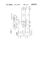
- FIG. 1 is a schematic diagram of the prior art memory device showing a part related to the present invention.
- a reference symbol QM shows a plurality of PROM cells arranged at intersection points of a matrix formed by a plurality of word-lines WL 0 through WL m and bit-lines BL 0 through BL n crossed each other.
- the decoders 1 and 2 produce column selecting signals Y 0 through Y n and row selecting signals X 0 through X m respectively.
- Column transfer gate transistors T 0 , T 1 , and T n are connected to bit-lines BL 0 , BL 1 , and BL n respectively, and each column transfer gate transistor consists of a field effect transistor having a source connected to both of a sense amplifier 3 and a programming circuit 4, a drain connected to the bit-line BL 0 , BL 1 , or BL n , and a gate connected to the column decoder 1 to receive the column selecting signal Y 0 , Y 1 , or Y n
- the address signal A is applied to the memory device, one of the row selecting signals X 0 through X m is applied to one of the word-lines W L through WL m , and one of the column selecting signals Y 0 through Y n is applied to a gate of one of the column transfer gate transistors T 0 through T n .
- a PROM cell When the memory device is in a state of programming a data signal given from the exterior of the memory device, the state will be called as "a programming mode" hereinafter, a PROM cell must be selected from the PROM cells arranged in the matrix, by both of a row selecting signal (X 0 , X 1 , or X m ) and a column selecting signal (Y 0 , Y 1 , or Y n ), and the programming circuit 4 is connected to the selected PROM cell by a selected column transfer gate transistor (T 0 , T 1 , or T n so that the data signal applied from the exterior of the memory device is transferred and programmed into the selected PROM cell.
- a row selecting signal X 0 , X 1 , or X m
- Y 0 , Y 1 , or Y n column selecting signal
- the PROM cell When the memory device is in a state of reading a data signal stored in a selected PROM cell, the state will be called as "a reading mode" hereinafter, the PROM cell is selected the same of the above, and the sensing amplifier is connected to the selected PROM cell by a selected column transfer gate transistor (T 0 , T 1 , or T n ) so that the data signal stored in the selected PROM cell is read out and transferred to the sense amplifier 3 and amplified.
- T 0 , T 1 , or T n selected column transfer gate transistor
- the source of every transfer gate transistor is connected to both of the sense amplifier 3 and the programming circuit 4.
- either of the sense amplifier 3 or the programming circuit 4 is selected by switching circuits, which are not depicted in FIG. 1, located in the sense amplifier 3 and the programming circuit 4 respectively and controlled by a read-write selecting signal 6 applied from the exterior of the memory device.
- FIG. 2 is a schematic diagram of the prior art showing the relation between the column decoder 1 and the selected column transfer gate transistor T i (i indicates one of the numerals 0 through n).
- the same reference numeral or symbol as in FIG. 1 designates the same unit or part as in FIG. 1, and a metal oxide semiconductor (MOS) transistor is used for all transistors; wherein, a transistor having no mark is an n-channel enhancement type transistor, a transistor having a black dot is an n-channel depletion type transistor, and a transistor having an arrow mark is a p-channel type transistor.
- MOS metal oxide semiconductor
- a power supply voltage V ppi for the NAND gate 101 and the buffer inverter 102 is variable.
- the power supply voltage V ppi becomes a high voltage (for example 21 volts (V)) so that the bit-line is held high with a high voltage (for example 15 V) for programming the data signal into the selected PROM cell.
- the voltage V ppi is switched to a low voltage (for example 5 V).
- a memory device is required to have a fast access time, particularly in the reading mode.
- the memory device cannot operate at high speed in the reading mode because the column transfer gate transistor is commonly used for programming and reading out the data signal.
- a large current is required to flow through the transistor T i , in the programming mode, for programming the data signal into the selected PROM cell on the bit-line BL i . Therefore, a channel width of the transistor T i must be large, which causes an increase in p-n junction capacitance formed between a substrate and a source or drain region of the transistor T i .
- This large stray capacitance becomes a heavy load for the sensing amplifier 3 and the PROM cell, so that a data sensing speed obtained in the sense amplifier 3 becomes slow. Furthermore, large capacitance formed between the gate of T 1 , T 2 , or T n and its channel also becomes a heavy load for the column decoder 1, so that a rise-time and a fall-time of the column selecting signal (Y i ) are lengthened, which also slow the data access time.
- a memory device having the PROM cells is usually used in the reading mode, and it is not necessary for the speed of programming the data signal into the selected PROM cell to be high. Thus, the problem stated above is how to realize the fast access time in the reading mode.
- An object of the present invention is to realize a faster access time of the memory device in the reading mode.
- the object is achieved by providing two groups of column transfer gate transistors. One is a first group of first column transfer gate transistors for programming the data signals into the selected PROM cells, and the other is a second group of second column transfer gate transistors for reading the data signals from the PROM cells.
- the two groups are independently provided to the memory device.
- FIG. 1 is a schematic diagram of the prior art memory device
- FIG. 2 is a schematic diagram showing a part relating to a column decoder and a column transfer gate transistor of the memory device;
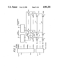
- FIG. 3 is a schematic diagram of a memory device firstly embodying the present invention.
- FIG. 4 is a schematic diagram showing a part relating to a column decoder and a column transfer gate transistor of the memory device firstly embodying the present invention
- FIG. 5 is a schematic diagram of a memory device secondly embodying the present invention.
- FIG. 6 is a schematic diagram showing a part relating to a column decoder and a column transfer gate transistor of the memory device secondly embodying the present invention.
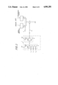
- FIG. 3 is a schematic diagram of a memory device firstly embodying the present invention.
- the same reference numeral or symbol as in FIG. 1 designates the same element or unit as in FIG. 1.
- the point of the present invention is that the column transfer gate transistors in the prior art memory device shown in FIG. 1 is independently separated into two groups: a first group of first column transfer gate transistors T W0 through TW n and a second group of second column transfer gate transistors T S0 through T Sn as shown in FIG. 3.
- the first column transfer gate transistor T W0 , T w1 , or T wn is for transferring a data signal from the programming circuit 4 to the selected PROM cell on a bit-line BL 0 , BL 1 , or BL n in the programmingmode
- the second column transfer gate transistor T S0 , T S1 , orT Sn is for reading out and transferring a data signal stored in a selected PROM cell on the bit-line BL 0 , BL 1 , or BL n using the sense amplifier 3 in the reading mode.
- the first column transfer gate transistors T W0 through TW n and the second column transfer gate transistors T S0 through T Sn are selected by a write column selecting signal WY 0 , WY 1 , or WY n and a read column selecting signals RY 0 , RY 1 , or RY n respectively.
- the write and read column selecting signals are provided in a column decoder 1-2.
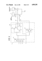
- FIG. 4 is a schematic diagram showing a part relating to the column decoder1-2, a first column transfer gate transistor T Wi , and a second column transfer gate transistor T Si of the memory device firstly embodying the present invention.
- the same reference numeral or symbol as in FIG. 3 designates the same unit or part as in FIG. 3, all transistors comprise the MOS transistors and their symbols such as the black dot and the arrow indicate the same kinds of the transistors as in FIG. 2.
- the column decoder 1-2 has two NAND gates 103 and104 and two buffer inverters 105 and 106.
- the NAND gate 103 and the buffer inverter 105 are for the programming mode
- the NAND gate 104 and the buffer inverter 106 are for the reading mode. Therefore, a high power supply voltage V pp (21V for example) is applied to both of the NAND gate 103 and the buffer inverter 105 and a low power supply voltage V cc (5 V for example) is applied to both of the NAND gate 104 and thebuffer inverter 106.
- the address signal A consisting of binary signals a i , a j , and a k is applied to both of the NAND gates 103 and104.
- the NAND gate 103 cannot make flow its current because the level of the inverted reading signal Rbecomes L, and the read-write selecting signal 6 selects the sense amplifier to operate. Accordingly, the data signal stored in the selected PROM cell is read out and amplified.
- the address signal A designates the address of the selecting PROM cell and the memory device is in the programming mode
- the NAND gate 103 makes flow a current because the level of the inverted reading signal Rbecomes H. Therefore, the output of the buffer inverter 105, which is equal to a write column selecting signal WY i , outputs an H level, so that the first column transfer gate transistor T Wi becomes conductive.
- the NAND gate 104 and the second column transfer gate transistor T Si also operate as stated above. However, only the programming circuit 4 operates because of the read-writeselecting signal 6. In the above, even though the currents ineffectively flow through the NAND gate 104, the buffer inverter 106, and the second column transfer gate transistor T Si wasting the power consumption of the memory device, the ineffective power consumption does not make much difference to the power consumption in the all memory device. Because the first column transfer gate transistor T Wi wastes more current than the above ineffective currents in the programming mode.
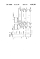
- FIG. 5 is a schematic diagram of a memory device secondly embodying the present invention.
- the same reference numerals or symbol as in FIG. 3 designates the same element or unit as in FIG. 3.
- FIG. 6 is a schematic diagram showing a part relating to a column decoder 1-3 and the first and the second column transfer gate transistors T Wi and T Si shown in FIG. 5.
- the same reference numeral or symbol as in FIG. 4 designates the same element or unit as in FIG. 4.
- the column decoder 1-3 consists of a NAND gate 107, a switching buffer inverter 108, and a buffer inverter 109 as shown in FIG. 6.
- the second embodiment there is only one NAND gate, which is apoint different from the first embodiment having two NAND gates.
- the address designated by the address signal A consisting of the signals a i , a j , and a k coincides with the address of the selecting PROM cell placed on the bit-line BL i and the memory device is in the programming mode
- the output of the NAND gate 107 becomes an L level
- a read signal R is in an L level
- the output of the switching buffer inverter 108 which is equal to a write column selecting signal WY i , becomes an H level, which allows to make the first column transfer gate transistor T Wi conductive.
- the second column transfer gate transistor T Si also becomes conductive.
- the programmingcircuit 4 operates because of the read-write selecting signal 6.
- the address signal A designates the address of the selecting PROM cell and thememory device is in the reading mode
- the level of the read signal R becomes equal to the V pp level, so that the write column selecting signal WY i becomes an L signal, which makes the first column transfergate transistor T wi non-conductive and only the second column transfergate transistor T Si is conductive.
- the second column transfer gate transistor T Si can be made in a narrow channel width because the transistor T Si requires only a little current to transfer the data signal from the selected PROM cell to the sense amplifier 3. Therefore, the load for the sensing amplifier 3 becomesdrastically lighter than that in the prior art. Accordingly, the data sensing speed becomes very fast. Furthermore, for the column decoder 1-2 or 1-3, the load capacitor becomes light, so that both of the rise-time and the fall-time of the read column selecting signal RY i are shorterthan those of the column selecting signals of the prior art.
- the stray capacitance of the second columntransfer gate transistor T S0 , T S1 , or T Sn becomes approximately one eighth of the first column transfer gate transistor T W0 , T W1 , or T Wn . Therefore, the memory access time is improved to 120 nanoseconds (n-sec) from 150 n-sec which is the time required in the prior art.
- a current flowing through the second column transfer gate transistor is 100 microamperes.
- a current flowing through the first column transfer gate transistor is several milliamperes. Since the column transfer gate transistors T 0 through T n of the prior art are separated into two groups in the present invention, the size of the memory device chip increases a little. However, in the first embodiment for example, the increasing ratio is several percent compared with the prior art. The value of several percent is small compared with twenty percent of the improved ratio of the access time.
Applications Claiming Priority (2)
| Application Number | Priority Date | Filing Date | Title |
|---|---|---|---|
| JP60179442A JPS6240698A (ja) | 1985-08-16 | 1985-08-16 | 半導体記憶装置 |
| JP60-179442 | 1985-08-16 |
Related Parent Applications (1)
| Application Number | Title | Priority Date | Filing Date |
|---|---|---|---|
| US07262094 Continuation | 1988-10-19 |
Publications (1)
| Publication Number | Publication Date |
|---|---|
| US4901281A true US4901281A (en) | 1990-02-13 |
Family
ID=16065932
Family Applications (1)
| Application Number | Title | Priority Date | Filing Date |
|---|---|---|---|
| US07/353,163 Expired - Lifetime US4901281A (en) | 1985-08-16 | 1989-05-12 | Semiconductor memory device having two column transfer gate transistor groups independently provided for a sense amplifier and a programmed circuit |
Country Status (4)
| Country | Link |
|---|---|
| US (1) | US4901281A (ja) |
| EP (1) | EP0212451A3 (ja) |
| JP (1) | JPS6240698A (ja) |
| KR (1) | KR900004327B1 (ja) |
Cited By (4)
| Publication number | Priority date | Publication date | Assignee | Title |
|---|---|---|---|---|
| US5517449A (en) * | 1987-06-29 | 1996-05-14 | Kabushiki Kaisha Toshiba | Memory cell of nonvolatile semiconductor memory device |
| US5712818A (en) * | 1994-10-01 | 1998-01-27 | Samsung Electronics Co., Ltd. | Data loading circuit for partial program of nonvolatile semiconductor memory |
| US6034899A (en) * | 1987-06-29 | 2000-03-07 | Kabushiki Kaisha Toshiba | Memory cell of nonvolatile semiconductor memory device |
| US6545913B2 (en) | 1987-06-29 | 2003-04-08 | Kabushiki Kaisha Toshiba | Memory cell of nonvolatile semiconductor memory device |
Families Citing this family (9)
| Publication number | Priority date | Publication date | Assignee | Title |
|---|---|---|---|---|
| JPH0793018B2 (ja) * | 1988-03-14 | 1995-10-09 | 株式会社東芝 | 不揮発性半導体メモリ |
| US5022008A (en) * | 1989-12-14 | 1991-06-04 | Texas Instruments Incorporated | PROM speed measuring method |
| FR2665972B1 (fr) * | 1990-08-17 | 1992-10-16 | Sgs Thomson Microelectronics | Circuit de precharge de lecture pour memoire en circuit integre. |
| US5847998A (en) * | 1996-12-20 | 1998-12-08 | Advanced Micro Devices, Inc. | Non-volatile memory array that enables simultaneous read and write operations |
| US5867430A (en) * | 1996-12-20 | 1999-02-02 | Advanced Micro Devices Inc | Bank architecture for a non-volatile memory enabling simultaneous reading and writing |
| US5841696A (en) * | 1997-03-05 | 1998-11-24 | Advanced Micro Devices, Inc. | Non-volatile memory enabling simultaneous reading and writing by time multiplexing a decode path |
| EP1450373B1 (en) * | 2003-02-21 | 2008-08-27 | STMicroelectronics S.r.l. | Phase change memory device |
| US9431111B2 (en) | 2014-07-08 | 2016-08-30 | Ememory Technology Inc. | One time programming memory cell, array structure and operating method thereof |
| US10684709B2 (en) | 2015-12-22 | 2020-06-16 | Shenzhen Royole Technologies Co., Ltd. | Electronic bags |
Citations (14)
| Publication number | Priority date | Publication date | Assignee | Title |
|---|---|---|---|---|
| FR2413794A1 (fr) * | 1977-12-28 | 1979-07-27 | Us Energy | Electrode perfectionnee pour cellule electrochimique secondaire |
| US4319341A (en) * | 1979-04-25 | 1982-03-09 | Fujitsu Limited | Programming circuit for permanently storing data in a programmable read only memory |
| EP0050005A2 (en) * | 1980-10-15 | 1982-04-21 | Kabushiki Kaisha Toshiba | Semiconductor memory with improved data programming time |
| US4367538A (en) * | 1980-02-22 | 1983-01-04 | Fujitsu Limited | Semiconductor memory device |
| US4432070A (en) * | 1981-09-30 | 1984-02-14 | Monolithic Memories, Incorporated | High speed PROM device |
| US4435789A (en) * | 1980-08-14 | 1984-03-06 | Siemens Aktiengesellschaft | Circuit for a read-only memory organized in rows and columns to prevent bit line potentials from dropping |
| US4481609A (en) * | 1981-08-19 | 1984-11-06 | Fujitsu Limited | Semiconductor memory miniaturized by line groups and staggered cells |
| US4527256A (en) * | 1982-03-17 | 1985-07-02 | Itt Industries, Inc. | Electrically erasable memory matrix (EEPROM) |
| US4535259A (en) * | 1982-06-18 | 1985-08-13 | Seeq Technology, Inc. | Sense amplifier for use with a semiconductor memory array |
| US4558434A (en) * | 1983-01-31 | 1985-12-10 | Fujitsu Limited | Semiconductor memory device |
| US4616339A (en) * | 1984-02-03 | 1986-10-07 | U.S. Philips Corporation | Integrated circuit with improved programmable read-only memory |
| US4630085A (en) * | 1984-02-28 | 1986-12-16 | Nec Corporation | Erasable, programmable read-only memory device |
| US4758987A (en) * | 1984-12-13 | 1988-07-19 | Kabushiki Kaisha Toshiba | Dynamic semiconductor memory with static data storing cell unit |
| US4769789A (en) * | 1985-01-05 | 1988-09-06 | Fujitsu Limited | Semiconductor memory device having serial data input and output circuit |
-
1985
- 1985-08-16 JP JP60179442A patent/JPS6240698A/ja active Granted
-
1986
- 1986-08-06 EP EP86110870A patent/EP0212451A3/en not_active Ceased
- 1986-08-07 KR KR1019860006516A patent/KR900004327B1/ko not_active IP Right Cessation
-
1989
- 1989-05-12 US US07/353,163 patent/US4901281A/en not_active Expired - Lifetime
Patent Citations (14)
| Publication number | Priority date | Publication date | Assignee | Title |
|---|---|---|---|---|
| FR2413794A1 (fr) * | 1977-12-28 | 1979-07-27 | Us Energy | Electrode perfectionnee pour cellule electrochimique secondaire |
| US4319341A (en) * | 1979-04-25 | 1982-03-09 | Fujitsu Limited | Programming circuit for permanently storing data in a programmable read only memory |
| US4367538A (en) * | 1980-02-22 | 1983-01-04 | Fujitsu Limited | Semiconductor memory device |
| US4435789A (en) * | 1980-08-14 | 1984-03-06 | Siemens Aktiengesellschaft | Circuit for a read-only memory organized in rows and columns to prevent bit line potentials from dropping |
| EP0050005A2 (en) * | 1980-10-15 | 1982-04-21 | Kabushiki Kaisha Toshiba | Semiconductor memory with improved data programming time |
| US4481609A (en) * | 1981-08-19 | 1984-11-06 | Fujitsu Limited | Semiconductor memory miniaturized by line groups and staggered cells |
| US4432070A (en) * | 1981-09-30 | 1984-02-14 | Monolithic Memories, Incorporated | High speed PROM device |
| US4527256A (en) * | 1982-03-17 | 1985-07-02 | Itt Industries, Inc. | Electrically erasable memory matrix (EEPROM) |
| US4535259A (en) * | 1982-06-18 | 1985-08-13 | Seeq Technology, Inc. | Sense amplifier for use with a semiconductor memory array |
| US4558434A (en) * | 1983-01-31 | 1985-12-10 | Fujitsu Limited | Semiconductor memory device |
| US4616339A (en) * | 1984-02-03 | 1986-10-07 | U.S. Philips Corporation | Integrated circuit with improved programmable read-only memory |
| US4630085A (en) * | 1984-02-28 | 1986-12-16 | Nec Corporation | Erasable, programmable read-only memory device |
| US4758987A (en) * | 1984-12-13 | 1988-07-19 | Kabushiki Kaisha Toshiba | Dynamic semiconductor memory with static data storing cell unit |
| US4769789A (en) * | 1985-01-05 | 1988-09-06 | Fujitsu Limited | Semiconductor memory device having serial data input and output circuit |
Non-Patent Citations (3)
| Title |
|---|
| IBM Technical Disclosure Bulletin, vol. 18, No. 6, Nov. 1975. * |
| LSI Memories, 2311 Fujitsu Scientific & Technical Journal, 21 (1985), Jul. No. 3, Kawasaki, Japan, pp. 337 369. * |
| LSI Memories, 2311 Fujitsu Scientific & Technical Journal, 21 (1985), Jul. No. 3, Kawasaki, Japan, pp. 337-369. |
Cited By (12)
| Publication number | Priority date | Publication date | Assignee | Title |
|---|---|---|---|---|
| US5517449A (en) * | 1987-06-29 | 1996-05-14 | Kabushiki Kaisha Toshiba | Memory cell of nonvolatile semiconductor memory device |
| US6011747A (en) * | 1987-06-29 | 2000-01-04 | Kabushiki Kaisha Toshiba | Memory cell of non-volatile semiconductor memory device |
| US6021073A (en) * | 1987-06-29 | 2000-02-01 | Kabushiki Kaisha Toshiba | Memory cell of non-volatile semiconductor memory device |
| US6034899A (en) * | 1987-06-29 | 2000-03-07 | Kabushiki Kaisha Toshiba | Memory cell of nonvolatile semiconductor memory device |
| US6058051A (en) * | 1987-06-29 | 2000-05-02 | Kabushiki Kaisha Toshiba | Memory cell of non-volatile semiconductor memory device |
| US6061271A (en) * | 1987-06-29 | 2000-05-09 | Kabushiki Kaisha Toshiba | Memory cell of nonvolatile semiconductor memory device |
| US6072748A (en) * | 1987-06-29 | 2000-06-06 | Kabushiki Kaisha Toshiba | Memory cell of nonvolatile semiconductor memory device |
| US6178116B1 (en) | 1987-06-29 | 2001-01-23 | Kabushiki Kaisha Toshiba | Memory cell of non-volatile semiconductor memory device |
| US6269021B1 (en) | 1987-06-29 | 2001-07-31 | Kabushiki Kaisha Toshiba | Memory cell of nonvolatile semiconductor memory device |
| US6545913B2 (en) | 1987-06-29 | 2003-04-08 | Kabushiki Kaisha Toshiba | Memory cell of nonvolatile semiconductor memory device |
| US6549462B1 (en) | 1987-06-29 | 2003-04-15 | Kabushiki Kaisha Toshiba | Memory cell of nonvolatile semiconductor memory device |
| US5712818A (en) * | 1994-10-01 | 1998-01-27 | Samsung Electronics Co., Ltd. | Data loading circuit for partial program of nonvolatile semiconductor memory |
Also Published As
| Publication number | Publication date |
|---|---|
| KR900004327B1 (ko) | 1990-06-22 |
| KR870002589A (ko) | 1987-03-31 |
| JPS6240698A (ja) | 1987-02-21 |
| JPH0323998B2 (ja) | 1991-04-02 |
| EP0212451A3 (en) | 1988-09-14 |
| EP0212451A2 (en) | 1987-03-04 |
Similar Documents
| Publication | Publication Date | Title |
|---|---|---|
| US4103189A (en) | Mos buffer circuit | |
| EP0090116B1 (en) | Cmis semiconductor device with two power supplies | |
| EP1047079B1 (en) | Semiconductor memory device generating accurate internal reference voltage | |
| KR0179361B1 (ko) | 비휘발성 메모리 어레이 | |
| KR900003932B1 (ko) | 개량된 기입확인 동작 반도체 메모리장치 | |
| EP0055594B1 (en) | Electrically programmable non-volatile semiconductor memory device | |
| US4901281A (en) | Semiconductor memory device having two column transfer gate transistor groups independently provided for a sense amplifier and a programmed circuit | |
| JPH0241113B2 (ja) | ||
| EP0072763A2 (en) | Semiconductor memory device | |
| US4901284A (en) | Static random access memory | |
| US4782247A (en) | Decoder circuit having a variable power supply | |
| JP2919299B2 (ja) | 列電圧保持回路を有する集積回路メモリ | |
| US4987560A (en) | Semiconductor memory device | |
| KR100300696B1 (ko) | 반도체기억장치 | |
| WO2008032069A1 (en) | Non-volatile memory bitcell | |
| JPH1011993A (ja) | 半導体記憶装置 | |
| US4982365A (en) | Semiconductor memory device with a potential level-setting circuit | |
| US5038327A (en) | Decoder circuit of erasable programmable read only memory for avoiding erroneous operation caused by parasitic capacitors | |
| US20020021584A1 (en) | Circuit structure for providing a hierarchical decoding in semiconductor memory devices | |
| US5265061A (en) | Apparatus for preventing glitch for semiconductor non-volatile memory device | |
| EP0317939B1 (en) | Input circuit incorporated in a semiconductor device | |
| EP0469834B1 (en) | A BICMOS logic circuit with self-boosting immunity and a method therefor | |
| EP0500468B1 (en) | Dual-port type semiconductor integrated memory circuit | |
| US6944041B1 (en) | Circuit for accessing a chalcogenide memory array | |
| US5301148A (en) | Semiconductor memory device with bipolar-FET sense amp |
Legal Events
| Date | Code | Title | Description |
|---|---|---|---|
| STCF | Information on status: patent grant |
Free format text: PATENTED CASE |
|
| CC | Certificate of correction | ||
| FEPP | Fee payment procedure |
Free format text: PAYOR NUMBER ASSIGNED (ORIGINAL EVENT CODE: ASPN); ENTITY STATUS OF PATENT OWNER: LARGE ENTITY |
|
| FPAY | Fee payment |
Year of fee payment: 4 |
|
| FPAY | Fee payment |
Year of fee payment: 8 |
|
| FPAY | Fee payment |
Year of fee payment: 12 |