US4535259A - Sense amplifier for use with a semiconductor memory array - Google Patents
Sense amplifier for use with a semiconductor memory array Download PDFInfo
- Publication number
- US4535259A US4535259A US06/389,819 US38981982A US4535259A US 4535259 A US4535259 A US 4535259A US 38981982 A US38981982 A US 38981982A US 4535259 A US4535259 A US 4535259A
- Authority
- US
- United States
- Prior art keywords
- voltage
- address
- bit line
- transistor
- voltage node
- Prior art date
- Legal status (The legal status is an assumption and is not a legal conclusion. Google has not performed a legal analysis and makes no representation as to the accuracy of the status listed.)
- Expired - Fee Related
Links
Images


Classifications
-
- G—PHYSICS
- G11—INFORMATION STORAGE
- G11C—STATIC STORES
- G11C7/00—Arrangements for writing information into, or reading information out from, a digital store
- G11C7/06—Sense amplifiers; Associated circuits, e.g. timing or triggering circuits
- G11C7/067—Single-ended amplifiers
Definitions
- the present invention is directed to a means for detecting the binary state of a selected storage device in a semiconductor memory array and more particularly concerns an amplifier circuit which functions to sense the presence or absence of current flow through the selected storage device during memory array read operations.
- a typical MOS floating gate storage device includes a floating gate structure disposed over the surface of a semiconductor substrate between spaced-apart source and drain regions.
- a control gate is then vertically aligned with the floating gate.
- Programming of the storage device is carried out by applying a potential to the control gate such that charge carriers are transported between the semiconductor substrate and the floating gate, whereupon the threshold voltage in the channel region established between the spaced-apart source and drain regions is modified.
- the presence or absence of charge carriers on the floating gate can be determined by simply measuring the presence or absence of current flow through the channel region in response to voltage potentials applied to the drain region.
- the memory array is prepared for programming or read operations by enabling the word line of a particular memory array row using a unique x-address applied to the address inputs of the memory array and by simultaneously enabling the bit line of a particular memory array column using a unique y-address also applied to the memory array address inputs. Thereafter, charge carriers can be transported to the floating gate of the storage device located at the intersection of the enabled word and bit lines through application of the aforementioned programming potential to the enabled word line. Alternately, the presence or absence of charge carriers on the floating gate of the storage device can be determined by connecting the enabled bit line to a source of read potential and then sensing whether current flows along the bit line through the storage device channel region. Current flow, it will be recalled, indicates that charge carriers are not present on the floating gate whereas the absence of current flow indicates that charge carriers have been placed on the floating gate.
- semiconductor memory arrays In order to determine whether current is flowing through an enabled bit line, and hence through a selected storage device connected to the enabled bit line, semiconductor memory arrays conventionally employ a sense amplifier to detect changes in bit line voltage and/or current levels. Although a variety of sense amplifier schemes may be utilized for this purpose, all such schemes are subject to several constraints. Specifically, an individual storage device in an unprogrammed state draws a minimal amount of current, generally on the order of 5 ⁇ a. Thus, the sense amplifier current source supplying the enabled bit line must be small enough to furnish the required current without overloading the individual storage device.
- the relatively large number of storage devices connected to the same bit line effectively places a cumulative capacitance of relatively large magnitude on the sense amplifier, which cumulative capacitance is progressively discharged as word lines associated with storage devices other than the selected storage device are enabled during memory array read operations.
- the sense amplifier current source is to provide current flow on the enabled bit line within the time constraints of practical semiconductor memory operation, an additional source of relatively large potential capable of rapidly charging the enabled bit line prior to reading the selected storage device is required. It is accordingly necessary to strike a balance between the competing demands of minimal current flow and rapid charge capacity when designing a sense amplifier for use with a semiconductor memory array.
- a sense amplifier comprising a sensing section, a reference signal generator and an inverting amplifier section.
- the sense amplifier sensing section includes a relatively small current transistor connected between a source of operating potential and a voltage node.
- the current transistor supplies a selected storage device connected to an enabled bit line in a semiconductor memory array with a read current having a magnitude adequate to perform the memory array read operation but not large enough to overload the selected storage device.
- the sense amplifier sensing section also includes a larger voltage transistor connected in parallel with the current transistor between the source of operating voltage and the voltage node. The voltage transistor rapidly raises the bit line potential to an acceptable level when the bit line is first enabled.
- a third transistor also of relatively large size connected between the voltage node and the bit line serves as a transfer gate for read currents.
- the sense amplifier reference signal generator feeds the control gates of the voltage transistor and the transfer gate with a reference potential V ref to establish the quiescent bit line potential.
- the programmed or non-programmed state of the selected storage device can then be ascertained by sensing whether the voltage at the sensing section voltage node drops in response to current flow through the enabled bit line and selected storage device. Any voltage drop at the voltage node which does occur is detected and amplified by the inverting amplifier section of the sense amplifier.
- the inverting amplifier section may specifically include a three-stage single-ended amplifier functioning as an inverter, whereby sharp transistions between the memory array logical one state and the memory array logical zero state are achieved in response to relatively small shifts in voltage at the sensing section voltage node.
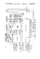
- FIG. 1 is a schematic representation of a semiconductor memory comprising floating gate storage devices arranged along primary and redundant word lines to form primary and redundant arrays;
- FIG. 2 is a circuit diagram of a dual-function address buffer capable of generating address and inverted address indicators and control signals for use in the semiconductor memory of the present invention
- FIG. 3 illustrates a representative Y-decoder for use with the semiconductor memory array of the present invention
- FIG. 4 is a circuit diagram of a representative portion of the column decoder employed in conjunction with the Y-decoder of FIG. 2 to enable selected bit lines of the semiconductor memory array in accordance with the y-address input to the memory array;
- FIG. 5 is a circuit diagram of the sense amplifier employed to detect the presence or absence of current flow through a selected storage device in the semiconductor memory array during memory array read operations.
- FIG. 1 schematically illustrates a semiconductor memory having a plurality of MOS storage devices 4 arranged to form a primary array 6.
- Each of the storage devices 4 may comprise an electrically-programmable read-only floating gate structure of the type disclosed in U.S. Pat. No. 4,288,256.
- a series of bit lines 8 arranged in columns and primary word lines 10 arranged in rows are respectively connected to the storage device drains 12 and control gates 14, whereby each storage device may be individually programmed and read in accordance with a unique storage device address.
- primary word lines 10 serve to define the x-addresses of the storage devices while bit lines 8 serve to define the storage device y-addresses.
- memory 2 includes two hundred and fifty-six primary word lines designated X 1 , X 2 . . . X 256 and two hundred and fifty-six bit lines designated Y 1 , Y 2 . . . Y 256 .
- the bit lines can be subdivided into eight groups of 32 bit lines each to enable the simultaneous storage of an 8-data bit word, i.e., a data byte, using only a single y-address.
- each of the eight bit lines activated by the single y-address may be arranged in interleaved fashion.
- Programming or reading of a particular storage device, or set of storage devices where bit lines 8 are divided into interleaved groups, is initiated by applying a digital address signal A 0 , A 1 . . . A n to a series of address bit inputs 16.
- the first five address bits A 0 -A 4 establish the particular y-address Y 1 , Y 2 . . . Y 32 of each data byte while an additional eight address bits A 5 -A 12 establish the data byte x-address A 1 , X 2 . . . X 256 .
- Address bit inputs 16 respectively feed the address bits A 0 -A 12 to a series of address buffers 18.
- Each of the address buffers in turn generates an address indicator AI i and an inverted address indicator AI i for use in decoding the address signal. That is, the output of the address buffers 18 which receive address bits A 0 -A 4 comprise a series of address indicators AI 0 -AI 4 and inverted address indicators AI 0 -AI 4 , whereas the output of the address buffers 18 which receive address bits A 5 -A 12 comprise a series of address indicators AI 5 -AI 12 and inverted address indicators AI 5 -AI 12 .
- Address indicators AI 5 -AI 12 and inverted address indicators AI 5 -AI 12 are supplied to X-decoders schematically illustrated at 20 and are combined in a digital logic system to enable the specific primary word line 10 associated with the x-address established by address bits A 5 -A 12 .
- the address indicators AI 0 -AI 4 and inverted address indicators AI 0 -AI 4 are supplied to Y-decoders illustrated schematically at 22.
- the Y-decoders operate in conjunction with a column decoder 24, combining the various address and inverted address indicators in a digital logic system such that selected bit lines 8 associated with the y-address established by data bits A 0 -A 4 are enabled.
- Data is programmed into or read out of primary array 6 by connecting each enabled bit line 8 to the appropriate one of a pair of input/output buffers 26 respectively tied to output pads 28 and then entering or reading out the appropriate data bit O 0 -O 7 .
- the time required to program individual storage devices 4 in primary array 6 can be significantly reduced by increasing the programming voltage present on the primary word lines 10 associated with the individual storage devices 4.
- a series of word line charge pumps 30 driven by a high voltage oscillator 31 are respectively connected to primary word lines 10 in order to raise the voltages thereof to a predetermined level during memory programming operations.
- Memory 2 is additionally provided with a redundant array 32 of storage devices 4 arranged along redundant word lines 34 for the purpose of providing back-up memory capacity should any of the primary word lines 10 in primary array 6 prove faulty, i.e., should any of the storage devices 4 associated with primary word lines 10 contain manufacturing defects.
- the redundant word lines 34 are connected to the control gates 14 of storage devices 4 to establish alternate x-addresses for the memory.
- address indicators AI 5 -AI 12 and inverted address indicators AI 5 -AI 12 generated by address buffers 18 as a function of the address bits A 5 -A 12 corresponding to the x-address of the faulty primary word line are used to program a redundancy decoder 36 such that any subsequent address signal A 0 -A 12 having the x-address of the faulty word line in primary array 6 will instead enable a selected redundant word line 34 in redundant array 32.
- a series of control signals supplied to redundancy select lines 37 via the output pads 28 associated with data bits O 0 -O 3 are gated through a set of redundancy enable transistors 38 to assist in programming redundancy decoder 36.
- a redundancy disable circuit 39 prevents any accidental reprogramming of redundancy decoder 36 relative to the selected redundant word line 34 enabled by the particular x-address.
- the redundancy disable circuit also generates a redundancy disable signal RD 1 -RD 4 indicative of the fact that the selected redundant word line is in use, which redundancy disable signal can be supplied back through redundancy enable transistors 38 to an appropriate output pad 28.
- the address buffers 18 employed in the memory 2 of the present invention may be constructed with a dual function capability, providing control signals for governing the operation of various peripheral circuits of the memory in addition to the aforementioned address and inverted address indicators AI 0 -AI 12 , AI 0 -AI 12 .
- FIG. 2 a representative address buffer 40 can be seen, it being understood that all of the address buffers 18 of FIG. 1 are similarly constructed.
- Address buffer 40 includes a conventional buffer/amplifier circuit 42 which receives an incoming address bit A i via input lead 44 and outputs an address indicator AI i in response thereto.
- the address indicator AI i switches either high or low depending upon whether address bit A i is a binary zero or a binary one.
- An inverter 46 connected to the output of buffer/amplifier circuit 42 provides the inverted address indicator AI i .
- the value of inverted address indicator AI i is, of course, low whenever the value of address indicator AI i is high and vice versa.
- Address buffer 40 further includes a high voltage detector 48 which detects high voltage inputs to the address buffer, i.e., voltages significantly greater than the TTL voltages employed in conjunction with address bits A i .
- the high voltage detector output comprises an inverted control signal RA i which may be used for control purposes by other peripheral circuits in memory 2.
- Inverted control signal RA i is passed through an inverter 49 to produce control signal RA i , and is simultaneously supplied to the control gates of pull-down transistors 50, 52 respectively connected across address indicator and inverted address indicator leads 54, 56.
- the address buffer of the present invention thus operates in two modes. When normal TTL voltages in the form of A i address bits are present on input lead 44, address buffer 40 outputs an address indicator AI i and an inverted address indicator AI i having complementary values determined in accordance with the binary state of address bit A i .
- the inverted control signal RA i from high voltage detector 48 switches high to perform the aforementioned peripheral control functions
- the control signal RA i from inverter 49 switches low to perform other peripheral control functions and pull-down transistors 50 and 52 are gated into conduction by inverted control signal RA i to disable the address and inverted address indicators AI i , AI i .
- the interleaved 64k-bit embodiment of memory 2 is characterized by thirty-two y-addresses Y 1 -Y 32 established in response to the first five address bits A 0 -A 4 of the digital address signal A 0 -A 12 input to address buffers 18.
- the bit lines 8 of memory 2 are correspondingly divided into eight groups of thirty-two bit lines each such that one bit line from every group of thirty-two bit lines will be enabled by a given y-address.
- each group of thirty-two bit lines in memory 2 is further sub-divided into two sub-groups of sixteen bit lines.
- the first four address bits A 0 -A 3 are utilized to access a selected one of the bit lines in each sub-group of sixteen bit lines while the remaining A 4 address bit is employed to access one of the two sub-groups of sixteen bit lines in each thirty-two bit line group.
- Y-decoders 22 receive the four address indicators AI 0 -AI 3 and inverted address indicators AI 0 -AI 3 output from the A 0 -A 3 address buffers. The address and inverted address indicators are thereafter processed by the Y-decoders to generate sixteen y-select signals YS 1 , YS 2 . . . YS 16 which respectively access the aforementioned one of sixteen bit lines in each sub-group of sixteen bit lines.
- the AI 4 address indicator and the AI 4 inverted address indicator output from the A 4 address buffer are directed to column decoder 24 for use in accessing the aforementioned one of the two bit line sub-groups in each group of thirty-two bit lines.
- Y-decoder 58 specifically generates the YS 1 and YS 2 y-select signals.
- Y-decoder 58 includes a y-select line 60 and a y-select line 62 tied to a common lead 64 via voltage node 66.
- Zero-threshold devices 68 and 70 are respectively connected across y-select lines 60 and 62.
- a pair of enhancement-mode devices 72 and 74 are in turn respectively connected between the y-select lines and the control gates of zero-threshold devices 68 and 70.
- the control gate of zero-threshold device 68 receives the AI 0 inverted address indicator while the control gate of enhancement-mode device 72 receives the AI 0 address indicator.
- the AI 0 address indicator is also supplied to the control gate of zero-threshold device 70, while the control gate of enhancement-mode device 74 receives the inverted address indicator AI 0 .
- a series of enhancement-mode devices 76, 78 and 80 are all connected in pull-down configuration between common lead 64 and ground.
- a depletion-mode device 82 is connected in pull-up configuration between lead 64 and an operating voltage supply line 84 carrying operating voltage V.sub. cc.
- the control gates of enhancement-mode devices 76-80 respectively receive the AI 1 , AI 2 and AI 3 address indicators.
- the binary states of the A 0 -A 3 address bits input to address buffers 18 determine which of the y-select signals YS 1 -YS 16 will be generated.
- a "0000" value for the A 0 -A 3 address bits will result in the generation of a high YS 1 signal on the y-select line 60. This result follows from the fact that the AI 0 -AI 3 address indicators output from address buffers 18 are all low when the A 0 -A 3 address bits are zero.
- enhancement-mode devices 76-80 will be rendered non-conductive and the voltage at voltage node 66 will be raised to V cc by the pull-up action of depletion-mode device 82.
- Zero-threshold device 68 will be rendered conductive by the high AI 0 inverted address indicator output from address buffers 18 when the A 0 address bit is zero, transferring the voltage V cc from voltage node 66 to the y-select line 60.
- zero-threshold device 70 will be rendered non-conductive by the low voltage AI 0 address indicator supplied to the control gate of zero-threshold device 70 while enhancement-mode device 74 conducts in response to the high AI 0 inverted address indicator.
- the AI 0 address indicator potential is thus applied to the y-select line 62, ensuring that the y-select signal YS 2 remains at a low value.
- the resulting high AI 0 address indicator and low or zero AI 0 inverted address indicator will combine to gate the V cc voltage at voltage node 66 through zero-threshold device 70 to generate a high y-select signal YS 2 on the y-select line 62 while driving the voltage, and hence the y-select signal YS 1 , on the y-select line 60 to zero.
- FIG. 3 specifically illustrates circuitry for generating the YS 1 and YS 2 y-select signals, it is understood that structurally similar circuitry receiving other logical permutations of the AI 0 -AI 3 address indicators and AI 0 -AI 3 inverted address indicators may be employed by Y-decoders 22 to generate the remaining y-select signals YS 3 -YS 16 .
- the various y-select signals YS 1 -YS 16 are used to gate transistors connected across the bit lines in each sub-group of sixteen bit lines.
- a relatively high potential to the selected bit lines in the various sub-groups of sixteen bit lines.
- Such high programming potentials require that the y-select transistors connected to the bit lines be heavily gated on during programming.
- the potential on the various y-select lines must be increased above the operating voltage V cc supplied by operating voltage supply line 84 in the Y-decoder circuitry of FIG. 3. Accordingly, the FIG.
- 3 circuitry includes two pairs of series-connected transistors 86, 88 arranged in pull-up configuration between a programming voltage supply line 90 carrying programming voltage V pp and the y-select lines 60, 62.
- Each transistor 86 is a zero-threshold device and each transistor 88 is a depletion-mode device.
- the control gates of the zero-threshold devices 86 are connected to a voltage node 92.
- a pull-up styled depletion-mode device 94 interconnects voltage node 92 with programming voltage supply line 90, while an enhancement-mode device 96 is connected in pull-down configuration to voltage node 92.
- the control gate of enhancement-mode device 96 receives an inverted programming signal PGM of the type frequently employed with programmable read-only memories.
- PGM is high and voltage node 92 is grounded to inactivate the zero-threshold devices 86, leaving the potential of the y-select lines 60 and 62 unaffected.
- the inverted programming signal PGM is driven low to remove the ground from voltage node 92, permitting depletion-mode device 94 to transfer the programming voltage V pp from programming voltage supply line 90 to the gates of the zero-threshold devices 86.
- the zero-threshold devices 86 are subsequently gated into conduction and the programming voltage V pp is supplied in pull-up fashion to the y-select lines 60 and 62.
- Either y-select line pulled down to zero voltage due to the aforementioned conduction of enhancement-mode devices 72 or 74 will remain at a zero potential, but if one of the y-select lines has instead been supplied with operating voltage V cc to generate the high y-select signal YS 1 or YS 2 , the y-select line so supplied will be driven to the V pp voltage level by the action of the zero-threshold devices 86 connected thereto. In this manner, the potential of the y-select signal YS 1 or YS 2 will be sufficient to ensure accurate programming of the selected memory device along the bit line enabled by the YS 1 or YS 2 y-select signal.
- FIG. 4 A representative portion of the column decoder 24 employed in memory array 2 is illustrated in detail in FIG. 4.
- Column decoder 24 operates in conjunction with Y-decoders 22 to enable selected bit lines 8 as a function of the y-address established by data bits A 0 -A 4 .
- bit lines 8 are divided into eight groups of thirty-two bit lines each.
- each group of thirty-two bit lines is further sub-divided into two sub-groups of sixteen bit lines each.
- One bit line in each group of thirty-two bit lines can then be enabled for each y-address Y i input to address buffers 18 by first accessing one bit line in each sub-group of sixteen bit lines and then accessing one sub-group in each group of thirty-two bit lines.
- bit lines 8 respectively associated with y-addresses Y 1 , Y 2 . . . Y 32 are consecutively arranged to form the eight groups 98 of thirty-two bit lines each such that the eight bit lines associated with each Y i address are interleaved.
- the first sixteen bit lines Y 1 -Y 16 in each group 98 for a first sub-group 100 of sixteen bit lines and the next sixteen bit lines Y 17 -Y 32 in each group 98 form a second sub-group 101 of sixteen bit lines.
- Bit lines Y 1 -Y 16 of sub-group 100 are respectively connected through a series of column-select transistors to a sub-group lead 102.
- control gates of column-select transistors 104 and 112 both receive the YS 1 y-select signal
- the control gates of column-select transistors 106 and 114 both receive the YS 2 y-select signal, and so on.
- Sub-group leads 102 and 110 are respectively connected through additional column-select transistors 118 and 120 to a sense line 122.
- Sense line 122 is connected to the sense amplifier 124 of the present invention, disclosed in greater detail in FIG. 5 below, for use during memory array read operations.
- the control gates of column-select transistors 118 and 120 are not commonly connected. Rather, the control gate of column-select transistor 118 receives the inverted address indicator AI 4 from the A 4 address buffer and the control gate of column-select transistor 120 receives the address indicator AI 4 from the A 4 address buffer.
- each bit line in each group 98 of thirty-two bit lines will be enabled for reading, i.e., connected to sense line 122, for each y-address input to memory 2.
- One of the column-select transistors 104-108 and 112-116 in each sub-group 100 or 101 of bit lines is gated by the associated y-select signal YS 1 -YS 16 output from the Y-decoders 22 in accordance with the A 0 -A 3 address bits supplied to the A 0 -A 3 address buffers 18, and either column-select transistor 118 or column-select transistor 120 is gated into conduction by the address indicators AI 4 , AI 4 from the A 4 address buffer 18 depending upon the binary state of the A 4 address bit supplied to the A 4 address buffer.
- y-decoder 22 will generate a high YS 1 y-select signal using the AI 0 -AI 3 address indicators and AI 0 -AI 3 inverted address indicators as described in conjunction with FIG. 3.
- the high YS 1 y-select signal gates column-select transistors 104 and 112.
- the "0" value of the A 4 address bit will cause the A 4 address buffer 18 to generate a low AI 4 address indicator together with a high AI 4 inverted address indicator as described in conjunction with FIG. 2.
- the column-select transistors 104 and 112 will still be gated by a high YS 1 y-select signal but the ensuing low AI 4 inverted address indicator together with the high AI 4 address indicator will now bias the column-select transistor 120 into conduction while shutting the column-select transistor 118 off, connecting the Y 17 bit line in group 98 rather than the Y 1 bit line to sense line 122 in preparation for reading a selected storage device tied to the Y 17 bit line.
- Programming of a selected memory device 4 along a selected Y 1 -Y 32 bit line is accomplished by switching on either of two programming transistors 126 or 128. More particularly, programming transistor 126 is connected between sub-group lead 102 and a programming voltage supply line 130 carrying programming voltage V pp . Programming transistor 128 is connected between sub-group lead 110 and programming voltage supply line 130. Programming transistor 126 can be biased into conduction by a depletion-mode device 132 connected in pull-up configuration between programming voltage supply line 130 and the control gate 134 of programming transistor 126.
- a pair of enhancement-mode pull-down devices 136 and 138 are also connected to the control gate 134 of programming transistor 126 such that conduction of either pull-down device 136 or 138 grounds control gate 134 and shuts programming transistor 126 off.
- the control gates of pull-down devices 136 and 138 are respectively connected to receive the AI 4 address indicator from the A 4 address buffer 18 and a data signal from the input/output buffer 26 (not shown in FIG. 4) associated with the 0 i data bit.
- depletion-mode pull-up device 140 and a pair of enhancement-mode pull-down devices 142 and 144 are tied to the control gate 146 of programming transistor 128 to govern the conduction thereof.
- the control gate of pull-down device 142 receives the 0 i data bit from the input/output buffer 26, but the control gate of pull-down device 144 receives the inverted address indicator AI 4 from the A 4 address buffer rather than the address indicator AI 4 .
- the y-address of the memory device is furnished to address inputs 16 and the corresponding y-select signal YS i is generated in response to the AI 0 -AI 3 and AI 0 -AI 3 address and inverted address indicators as disclosed hereinabove to gate the appropriate one of the column-select transistors 104-108 and 112-116 in each sub-group 100, 101 of sixteen bit lines.
- the complementary values of the AI 4 and AI 4 address and inverted address indicators will act to bias one of the two pull-down devices 136 and 144 on while rendering the other of the two pull-down devices non-conductive.
- the control gate 134 or 146 tied to the conducting pull-down device 136 or 144 will be grounded to turn the associated programming transistor 126 or 128 off.
- the remaining control gate cannot be grounded through the non-conductive pull-down device 136 or 144 tied thereto, and the programming transistor associated with the remaining control gate is consequently gated into conduction depending upon the value of the 0 i data bit. If 0 i is low, i.e., has a "zero" value, pull-down devices 138 and 142 will also be rendered non-conductive to remove the last ground from the remaining control gate, whereupon depletion-mode device 132 or 140 will operate to raise the voltage on the remaining control gate and bias the associated programming transistor into conduction.
- the programming voltage V pp on programming voltage supply line 130 is thereafter transferred from the programming voltage supply line 130 through the appropriate sub-group lead 102 or 110 and the gated column-select transistor in the corresponding series of column-select transistors 104-108 or 112-116 to the selected Y i bit line, enabling programming of the selected memory device 4 along the Y i bit line. If the 0 i data bit has a "one" value, both pull-down devices 138 and 142 will be biased on to ground the control gates 134 and 146 of programming transistors 126 and 128 without regard to whether pull-down device 136 or 144 is conducting and the programming voltage V pp will be prevented from reaching the selected Y i bit line.
- the column-select transistor 118 or 120 connected to the sub-group lead 102 or 110 receiving the programming voltage V pp will itself be supplied with a high gate drive signal.
- This high gate drive signal will, however, not result in the conduction of the column-select transistor 118 or 120, inasmuch as the magnitude of V pp is greater than the magnitude of either the AI 4 or AI 4 signal and the gate-to-source voltage on column-select transistors 118 or 120 will always be less than zero.
- the low AI 4 address indicator generated in response to the "0" A 4 address bit will render pull-down device 136 non-conductive to remove one source of ground from the control gate 134 of programming transistor 126 associated with the Y 1 bit line.
- the aforementioned value of the 0 i data bit will then determine whether the programming voltage V pp is transferred through programming transistor 126, sub-group lead 102 and column-select transistor 104 to the Y 1 bit line. That is, where 0 i has a binary "zero" value, pull-down device 138 is turned off and programming transistor 126 conducts to place the programming voltage V pp on the Y 1 bit line.
- the programming voltage causes transfer of charge carriers between the storage device channel region and the floating gate of the storage device, increasing the storage device threshold voltage beyond the value at which current flow through the selected storage device channel is produced when a read or sense voltage is applied to the storage device control gate.
- 0 i is a binary one
- pull-down device 138 conducts to ground control gate 134 and shut programming transistor 126 off. In the latter event, no programming voltage reaches the Y 1 bit line and no charge carriers are transported between the channel region and floating gate of the selected storage device. With the floating gate free of charge carriers, the threshold voltage of the selected storage device is lowered sufficiently to permit current flow through the storage device channel region when the read voltage is applied to the storage device control gate.
- pull-down device 144 is rendered non-conductive by the low AI 4 inverted address indicator to remove one source of ground from the control gate 146 of programming transistor 128.
- the conductive state of remaining pull-down device 142 determines the conductive state of programming transistor 128 as a function of the binary value of the 0 i data bit.
- Programming voltage V pp is transferred to the enabled Y 17 bit line when the 0 i data bit is a binary "zero" and blocked from the enabled Y 17 bit line when 0 i is a binary "one".
- FIG. 5 a representative sense amplifier 124 of the present invention can be seen.
- One such sense amplifier is utilized for each group 98 of thirty-two bit lines in the column decoder of FIG. 4.
- the sense amplifier functions during memory read operations to detect the presence or absence of current flow through a selected storage device connected to an enabled Y i bit line, thereby determining the binary state of the selected storage device.
- Sense amplifier 124 basically consists of a reference signal generator 148, a sensing section 150 and an inverting amplifier section 152.
- the reference signal generator which provides a reference voltage V ref for sense amplifier 124, comprises a pair of depletion-mode devices 154, 156 connected in series between ground and an operating voltage supply line 158 carrying operating voltage V cc .
- depletion-mode devices 154 and 156 are also grounded. Hence, depletion-mode devices 154 and 156 conduct until the voltage V ref at node 160 between the two devices reaches a level equal to approximately half that of the supply line voltage V cc .
- the width-to-length channel ratio of device 154 is somewhat smaller than the width-to-length channel ratio of device 156 and the threshold voltage of device 154 is correspondingly larger than the threshold voltage of device 156, causing V ref to drop slightly below the halfway value of V cc .
- V ref will be approximately 2 volts.
- the control gate of device 156 is grounded, a bleed current is constantly drawn through device 156 to enhance the stability of V ref at voltage node 160.
- Sensing section 150 of sense amplifier 124 comprises a voltage node 162 respectively connected to operating voltage supply line 158 through a depletion-mode device 164 arranged in pull-up configuration and to sense line 122 through a zero threshold device 166.
- a second zero-threshold device 168 is connected in parallel with depletion-mode device 164 between operating voltage supply line 158 and voltage node 162.
- the control gates of both zero-threshold devices 166 and 168 are connected to receive the reference potential V ref from voltage node 160 in the reference signal generator 148.
- depletion-mode device 164 serves as a current source for supplying read currents to an enabled Y i bit line during memory array read operations.
- Zero-threshold device 168 serves as a source of voltage for charging sense line 122 and the enabled Y i bit line, while zero-threshold device 166 functions as a transfer gate for clamping the voltage present on the sense line and for transferring read currents from depletion-mode device 164 to the enabled bit line. Because the current drawn through any individual storage device connected to the enabled Y i bit line is relatively small, depletion-mode device 164 must likewise be small if damage to the selected storage device is to be avoided during read operations.
- the total number of storage devices connected to the enabled Y i bit line represents a cumulative bit line capacitance of relatively large magnitude, which bit line capacitance is subject to significant discharge or leakage as various word lines associated with the storage devices are enabled during previous memory array read operations. It can accordingly be seen that some means of rapidly charging sense line 122 and the enabled Y i bit line to an adequate potential at the outset of any given read operation is required if read times are to remain compatible with other memory array processing operations. For this reason, zero-threshold devices 166 and 168 are designed to handle significantly larger voltages than depletion-mode device 164.
- V ref appearing at voltage node 160 in response to the powering-up of operating voltage supply line 158 causes zero-threshold devices 166 and 168 to begin conducting.
- the source voltage at both zero-threshold devices 166 and 168, and hence the voltage on sense line 122 and any enabled Y i bit line rapidly increases.
- the voltage at voltage node 162 can rise to the level of V cc due to the presence of depletion-mode device 164.
- the selected storage device on the enabled Y i bit line is programmed, i.e., if a binary zero is stored in the selected storage device, no current will flow along the enabled Y i bit line and the voltage at voltage node 162 will stabilize at the V cc level.
- V cc and V ref are sufficient to provide an indication of current flow through the selected storage device on the enabled Y i bit line.
- Inverting amplifier section 152 of sense amplifier 124 is designed to detect voltage shifts at voltage node 162, and for this purpose includes a series of three single-ended amplifier stages 170, 172 and 174.
- Amplifier stage 170 consists of depletion-mode device 176 connected in pull-up configuration between operating voltage supply line 158 and a voltage node 178 together with an enhancement-mode device 180 connected in pull-down configuration between voltage node 178 and ground.
- amplifier stages 172 and 174 consist of depletion-mode devices 182 and 184 respectively connected between operating voltage supply line 158 and voltage nodes 186 and 188, while enhancement-mode devices 190 and 192 are respectively connected between voltage nodes 186 and 188 and ground.
- the control gate of enhancement-mode device 180 in amplifier stage 170 is connected to voltage node 162 in sensing section 150.
- Voltage node 178 in amplifier stage 170 is connected to the control gate of enhancement-mode device 190 in amplifier stage 172
- voltage node 186 in amplifier stage 172 is connected to the control gate of enhancement-mode device 192 in amplifier stage 174
- voltage node 188 in amplifier stage 174 is connected to a data output lead 194.
- enhancement-mode device 180 When the voltage at voltage node 162 in the sensing section 150 of sense amplifier 124 is at V cc , indicating that no current is flowing through the enabled Y i bit line, enhancement-mode device 180 is heavily gated on and the potential at voltage node 178 in amplifier stage 170 of inverting amplifier section 152 is pulled low. The low potential at voltage node 178 biases enhancement-mode device 190 off, whereupon the pull-up action of depletion-mode device 182 raises the voltage at voltage node 186 to V cc and enhancement-mode device 192 is gated into conduction. Voltage node 188 is then pulled low to provide a low DATA-OUT signal indicative of a programmed or binary zero state for the selected storage device on the Y i bit line.
- Enhancement-mode device 190 in amplifier stage 172 thereafter begins conducting to pull the voltage at voltage node 186 down, removing the gate drive from enhancement-mode device 192 in amplifier stage 174 and permitting the pull-up action of depletion-mode device 184 to raise the voltage at voltage node 188.
- a high DATA-OUT signal indicative of a non-programmed or binary one state in the selected storage device is present on the data output lead 194.
- the DATA-OUT signal on the data output lead 194 may be supplied to the output section of input/output buffers 26 (not shown in FIG. 5) in memory array 2 and thence to the appropriate 0 i output pad 28 for use in data processing activities.
- zero-threshold devices 196 and 198 may be respectively interposed between the depletion-mode devices 176 and 184 on either end of the inverting amplifier section 152.
- Zero-threshold devices 196 and 198 serve as power-down transistors for the sense amplifier 124. Both of the zero-threshold devices are gated by a CHIP ENABLE signal CE which is conventionally supplied to semiconductor memory array 2 for the purpose of activating the array.
- CE signal is low, indicating a power-down or non-use condition for memory array 2
- zero-threshold devices 196 and 198 are gated off and depletion-mode devices 176 and 184 cannot conduct to raise the potential at voltage nodes 178 and 188.
- zero-threshold devices 196 and 198 are gated into conduction and the voltage potential on operating voltage supply line 158 is made available to the depletion-mode devices 176 and 184 in preparation for sense amplifier operation.
Landscapes
- Read Only Memory (AREA)
Abstract
Description
Claims (5)
Priority Applications (1)
| Application Number | Priority Date | Filing Date | Title |
|---|---|---|---|
| US06/389,819 US4535259A (en) | 1982-06-18 | 1982-06-18 | Sense amplifier for use with a semiconductor memory array |
Applications Claiming Priority (1)
| Application Number | Priority Date | Filing Date | Title |
|---|---|---|---|
| US06/389,819 US4535259A (en) | 1982-06-18 | 1982-06-18 | Sense amplifier for use with a semiconductor memory array |
Publications (1)
| Publication Number | Publication Date |
|---|---|
| US4535259A true US4535259A (en) | 1985-08-13 |
Family
ID=23539851
Family Applications (1)
| Application Number | Title | Priority Date | Filing Date |
|---|---|---|---|
| US06/389,819 Expired - Fee Related US4535259A (en) | 1982-06-18 | 1982-06-18 | Sense amplifier for use with a semiconductor memory array |
Country Status (1)
| Country | Link |
|---|---|
| US (1) | US4535259A (en) |
Cited By (19)
| Publication number | Priority date | Publication date | Assignee | Title |
|---|---|---|---|---|
| EP0177106A2 (en) * | 1984-10-05 | 1986-04-09 | Koninklijke Philips Electronics N.V. | Self referenced sense amplifier circuit |
| US4638191A (en) * | 1984-07-05 | 1987-01-20 | Hewlett-Packard Company | Amplitude insensitive delay line |
| US4754434A (en) * | 1985-08-28 | 1988-06-28 | Advanced Micro Devices, Inc. | Switching plane redundancy |
| US4788460A (en) * | 1986-03-24 | 1988-11-29 | Nec Corporation | Circuit arrangement of sense amplifier for rapid evaluation of logic state |
| US4800297A (en) * | 1986-06-03 | 1989-01-24 | Sgs Microelecttronica Spa | Source bias generator for natural transistors in MOS digital integrated circuits |
| US4823031A (en) * | 1988-02-01 | 1989-04-18 | Texas Instruments Incorporated | Single-ended sense amplifier with positive feedback |
| US4859882A (en) * | 1987-12-16 | 1989-08-22 | Kabushiki Kaisha Toshiba | Sense amplifier |
| US4901281A (en) * | 1985-08-16 | 1990-02-13 | Fujitsu Limited | Semiconductor memory device having two column transfer gate transistor groups independently provided for a sense amplifier and a programmed circuit |
| US4903237A (en) * | 1988-08-02 | 1990-02-20 | Catalyst Semiconductor, Inc. | Differential sense amplifier circuit for high speed ROMS, and flash memory devices |
| EP0399362A2 (en) * | 1989-05-16 | 1990-11-28 | Fujitsu Limited | A sense amplifier circuit |
| US5018104A (en) * | 1988-04-12 | 1991-05-21 | Nec Corporation | Redundant circuit incorporated in semiconductor memory device |
| USRE33725E (en) * | 1984-10-05 | 1991-10-22 | North American Philips Corporation | Self referenced sense amplifier |
| US5309400A (en) * | 1990-02-19 | 1994-05-03 | Fujitsu Limited | Sense circuit for non-volatile memory device |
| EP0690449A2 (en) * | 1994-06-28 | 1996-01-03 | Matsushita Electric Industrial Co., Ltd. | Sense amplifier for semiconductor memory device |
| US5495191A (en) * | 1994-03-25 | 1996-02-27 | Sun Microsystems, Inc. | Single ended dynamic sense amplifier |
| US5574633A (en) * | 1994-02-23 | 1996-11-12 | At&T Global Information Solubions Company | Multi-phase charge sharing method and apparatus |
| US20040093458A1 (en) * | 1999-02-18 | 2004-05-13 | Hitachi, Ltd. | Information processing apparatus using index and TAG addresses for cache |
| US20080159035A1 (en) * | 2006-12-27 | 2008-07-03 | Micron Technology, Inc. | Array sense amplifiers, memory devices and systems including same, and methods of operation |
| US20210118501A1 (en) * | 2019-10-22 | 2021-04-22 | Micron Technology, Inc. | Voltage Drivers with Reduced Power Consumption during Polarity Transition |
Citations (3)
| Publication number | Priority date | Publication date | Assignee | Title |
|---|---|---|---|---|
| US4223394A (en) * | 1979-02-13 | 1980-09-16 | Intel Corporation | Sensing amplifier for floating gate memory devices |
| JPS5767332A (en) * | 1980-10-15 | 1982-04-23 | Toshiba Corp | Semiconductor integrated circuit device |
| US4443718A (en) * | 1979-09-21 | 1984-04-17 | Hitachi, Ltd. | Nonvolatile semiconductor memory with stabilized level shift circuit |
-
1982
- 1982-06-18 US US06/389,819 patent/US4535259A/en not_active Expired - Fee Related
Patent Citations (3)
| Publication number | Priority date | Publication date | Assignee | Title |
|---|---|---|---|---|
| US4223394A (en) * | 1979-02-13 | 1980-09-16 | Intel Corporation | Sensing amplifier for floating gate memory devices |
| US4443718A (en) * | 1979-09-21 | 1984-04-17 | Hitachi, Ltd. | Nonvolatile semiconductor memory with stabilized level shift circuit |
| JPS5767332A (en) * | 1980-10-15 | 1982-04-23 | Toshiba Corp | Semiconductor integrated circuit device |
Cited By (31)
| Publication number | Priority date | Publication date | Assignee | Title |
|---|---|---|---|---|
| US4638191A (en) * | 1984-07-05 | 1987-01-20 | Hewlett-Packard Company | Amplitude insensitive delay line |
| USRE33725E (en) * | 1984-10-05 | 1991-10-22 | North American Philips Corporation | Self referenced sense amplifier |
| US4584493A (en) * | 1984-10-05 | 1986-04-22 | Signetics Corporation | Self referenced sense amplifier |
| EP0177106A3 (en) * | 1984-10-05 | 1988-02-24 | Koninklijke Philips Electronics N.V. | Self referenced sense amplifier circuit |
| EP0177106A2 (en) * | 1984-10-05 | 1986-04-09 | Koninklijke Philips Electronics N.V. | Self referenced sense amplifier circuit |
| US4901281A (en) * | 1985-08-16 | 1990-02-13 | Fujitsu Limited | Semiconductor memory device having two column transfer gate transistor groups independently provided for a sense amplifier and a programmed circuit |
| US4754434A (en) * | 1985-08-28 | 1988-06-28 | Advanced Micro Devices, Inc. | Switching plane redundancy |
| US4788460A (en) * | 1986-03-24 | 1988-11-29 | Nec Corporation | Circuit arrangement of sense amplifier for rapid evaluation of logic state |
| US4800297A (en) * | 1986-06-03 | 1989-01-24 | Sgs Microelecttronica Spa | Source bias generator for natural transistors in MOS digital integrated circuits |
| US4859882A (en) * | 1987-12-16 | 1989-08-22 | Kabushiki Kaisha Toshiba | Sense amplifier |
| US4823031A (en) * | 1988-02-01 | 1989-04-18 | Texas Instruments Incorporated | Single-ended sense amplifier with positive feedback |
| US5018104A (en) * | 1988-04-12 | 1991-05-21 | Nec Corporation | Redundant circuit incorporated in semiconductor memory device |
| US4903237A (en) * | 1988-08-02 | 1990-02-20 | Catalyst Semiconductor, Inc. | Differential sense amplifier circuit for high speed ROMS, and flash memory devices |
| EP0399362A3 (en) * | 1989-05-16 | 1991-03-20 | Fujitsu Limited | A sense amplifier circuit |
| US5293088A (en) * | 1989-05-16 | 1994-03-08 | Fujitsu Limited | Sense amplifier circuit |
| EP0399362A2 (en) * | 1989-05-16 | 1990-11-28 | Fujitsu Limited | A sense amplifier circuit |
| US5309400A (en) * | 1990-02-19 | 1994-05-03 | Fujitsu Limited | Sense circuit for non-volatile memory device |
| US5574633A (en) * | 1994-02-23 | 1996-11-12 | At&T Global Information Solubions Company | Multi-phase charge sharing method and apparatus |
| US5619149A (en) * | 1994-03-25 | 1997-04-08 | Sun Microsystems, Inc. | Single ended dynamic sense amplifier |
| US5495191A (en) * | 1994-03-25 | 1996-02-27 | Sun Microsystems, Inc. | Single ended dynamic sense amplifier |
| EP0690449A3 (en) * | 1994-06-28 | 1999-01-13 | Matsushita Electric Industrial Co., Ltd. | Sense amplifier for semiconductor memory device |
| EP0690449A2 (en) * | 1994-06-28 | 1996-01-03 | Matsushita Electric Industrial Co., Ltd. | Sense amplifier for semiconductor memory device |
| US20040093458A1 (en) * | 1999-02-18 | 2004-05-13 | Hitachi, Ltd. | Information processing apparatus using index and TAG addresses for cache |
| US7159067B2 (en) * | 1999-02-18 | 2007-01-02 | Hitachi, Ltd. | Information processing apparatus using index and TAG addresses for cache |
| US20080159035A1 (en) * | 2006-12-27 | 2008-07-03 | Micron Technology, Inc. | Array sense amplifiers, memory devices and systems including same, and methods of operation |
| US7606097B2 (en) | 2006-12-27 | 2009-10-20 | Micron Technology, Inc. | Array sense amplifiers, memory devices and systems including same, and methods of operation |
| US20100019804A1 (en) * | 2006-12-27 | 2010-01-28 | Micron Technology, Inc. | Array sense amplifiers, memory devices and systems including same, and methods of operation |
| US7894286B2 (en) | 2006-12-27 | 2011-02-22 | Micron Technology, Inc. | Array sense amplifiers, memory devices and systems including same, and methods of operation |
| US20210118501A1 (en) * | 2019-10-22 | 2021-04-22 | Micron Technology, Inc. | Voltage Drivers with Reduced Power Consumption during Polarity Transition |
| US11087838B2 (en) * | 2019-10-22 | 2021-08-10 | Micron Technology, Inc. | Voltage drivers with reduced power consumption during polarity transition |
| US11527286B2 (en) | 2019-10-22 | 2022-12-13 | Micron Technology, Inc. | Voltage drivers with reduced power consumption during polarity transition |
Similar Documents
| Publication | Publication Date | Title |
|---|---|---|
| US4535259A (en) | Sense amplifier for use with a semiconductor memory array | |
| US4538245A (en) | Enabling circuit for redundant word lines in a semiconductor memory array | |
| US5485425A (en) | Semiconductor memory device having redundant column and operation method thereof | |
| US4933906A (en) | Non-volatile semiconductor memory device | |
| US4905197A (en) | Semiconductor memory having circuitry for discharging a digit line before verifying operation | |
| US5502676A (en) | Integrated circuit memory with column redundancy having shared read global data lines | |
| JPS62132299A (en) | Sense amplifier for non-volatile memory | |
| US4879682A (en) | Sense amplifier precharge control | |
| EP0211232B1 (en) | Semiconductor memory in which data readout operation is carried out over wide power voltage range | |
| US5579266A (en) | Semiconductor memory device | |
| US7474553B2 (en) | Device writing to a plurality of rows in a memory matrix simultaneously | |
| JP3165489B2 (en) | Bias circuit for endurance memory array | |
| US4631707A (en) | Memory circuit with power supply voltage detection means | |
| KR0148605B1 (en) | Semiconductor memory device for maintaining level of signal line | |
| US4870618A (en) | Semiconductor memory equipped with test circuit for testing data holding characteristic during data programming period | |
| US6201747B1 (en) | Method and apparatus for measuring subthreshold current in a memory array | |
| KR900004327B1 (en) | Semiconductor memory device having column transfer gate transistor at sense amp and at programing circuit independanty | |
| US5572467A (en) | Address comparison in an inteagrated circuit memory having shared read global data lines | |
| US4489401A (en) | Electrical partitioning scheme for improving yields during the manufacture of semiconductor memory arrays | |
| US5426611A (en) | Non-volatile semiconductor device | |
| US5398204A (en) | Nonvolatile semiconductor system | |
| EP0443777A2 (en) | Write circuit for non-volatile memory device | |
| EP0640917B1 (en) | Roll call circuit for semi-conductor memory | |
| US5864507A (en) | Dual level wordline clamp for reduced memory cell current | |
| JP3238429B2 (en) | Semiconductor storage device |
Legal Events
| Date | Code | Title | Description |
|---|---|---|---|
| AS | Assignment |
Owner name: SEEQ TECHNOLOGY, INC., 1849 FOTUNE DRIVE, SAN JOSE Free format text: ASSIGNMENT OF ASSIGNORS INTEREST.;ASSIGNORS:SMARANDOIU, GEORGE;PERLEGOS, GEORGE;REEL/FRAME:004030/0443 Effective date: 19820903 |
|
| FPAY | Fee payment |
Year of fee payment: 4 |
|
| FEPP | Fee payment procedure |
Free format text: PAYOR NUMBER ASSIGNED (ORIGINAL EVENT CODE: ASPN); ENTITY STATUS OF PATENT OWNER: LARGE ENTITY |
|
| AS | Assignment |
Owner name: SILICON VALLEY BANK, CALIFORNIA Free format text: ASSIGNMENT OF ASSIGNORS INTEREST.;ASSIGNOR:SEEQ TECHNOLOGY, INCORPORATED;REEL/FRAME:006441/0970 Effective date: 19921124 |
|
| LAPS | Lapse for failure to pay maintenance fees | ||
| FP | Lapsed due to failure to pay maintenance fee |
Effective date: 19930815 |
|
| AS | Assignment |
Owner name: SEEQ TECHNOLOGY, INCORPORATED, CALIFORNIA Free format text: RELEASE BY SECURED PARTY;ASSIGNOR:SILICON VALLEY BANK;REEL/FRAME:006797/0240 Effective date: 19930224 |
|
| AS | Assignment |
Owner name: CIT GROUP/CREDIT FINANCING, INC., THE, CALIFORNIA Free format text: SECURITY INTEREST;ASSIGNOR:SEEQ TECHNOLOGY INCORPORATED;REEL/FRAME:006763/0733 Effective date: 19931122 |
|
| AS | Assignment |
Owner name: ATMEL CORPORATION, CALIFORNIA Free format text: ASSIGNMENT OF ASSIGNORS INTEREST;ASSIGNOR:SEEQ TECHNOLOGY INCORPORATED;REEL/FRAME:006863/0773 Effective date: 19940207 |
|
| AS | Assignment |
Owner name: SEEQ TECHNOLOGY INCORPORATED, CALIFORNIA Free format text: PARTIAL RELEASE OF SECURITY INTEREST;ASSIGNOR:CIT GROUP/CREDIT FINANCE, INC., THE;REEL/FRAME:006994/0849 Effective date: 19940304 Owner name: ATMEL CORPORATION, CALIFORNIA Free format text: ASSIGNMENT OF ASSIGNORS INTEREST;ASSIGNOR:SEEQ TECHNOLOGY INCORPORATED;REEL/FRAME:006975/0106 Effective date: 19940419 |
|
| FEPP | Fee payment procedure |
Free format text: PETITION RELATED TO MAINTENANCE FEES FILED (ORIGINAL EVENT CODE: PMFP); ENTITY STATUS OF PATENT OWNER: LARGE ENTITY |
|
| FEPP | Fee payment procedure |
Free format text: PETITION RELATED TO MAINTENANCE FEES DENIED/DISMISSED (ORIGINAL EVENT CODE: PMFD); ENTITY STATUS OF PATENT OWNER: LARGE ENTITY |
|
| FEPP | Fee payment procedure |
Free format text: PETITION RELATED TO MAINTENANCE FEES FILED (ORIGINAL EVENT CODE: PMFP); ENTITY STATUS OF PATENT OWNER: LARGE ENTITY |
|
| SULP | Surcharge for late payment | ||
| PRDP | Patent reinstated due to the acceptance of a late maintenance fee |
Effective date: 19970718 |
|
| SULP | Surcharge for late payment | ||
| FEPP | Fee payment procedure |
Free format text: PETITION RELATED TO MAINTENANCE FEES DENIED/DISMISSED (ORIGINAL EVENT CODE: PMFD); ENTITY STATUS OF PATENT OWNER: LARGE ENTITY |
|
| LAPS | Lapse for failure to pay maintenance fees |
Free format text: PATENT EXPIRED FOR FAILURE TO PAY MAINTENANCE FEES (ORIGINAL EVENT CODE: EXP.) |
|
| STCH | Information on status: patent discontinuation |
Free format text: PATENT EXPIRED DUE TO NONPAYMENT OF MAINTENANCE FEES UNDER 37 CFR 1.362 |