US4638191A - Amplitude insensitive delay line - Google Patents
Amplitude insensitive delay line Download PDFInfo
- Publication number
- US4638191A US4638191A US06/628,069 US62806984A US4638191A US 4638191 A US4638191 A US 4638191A US 62806984 A US62806984 A US 62806984A US 4638191 A US4638191 A US 4638191A
- Authority
- US
- United States
- Prior art keywords
- node
- coupled
- type mosfet
- depletion
- control means
- Prior art date
- Legal status (The legal status is an assumption and is not a legal conclusion. Google has not performed a legal analysis and makes no representation as to the accuracy of the status listed.)
- Expired - Lifetime
Links
- 238000009738 saturating Methods 0.000 claims abstract description 19
- 230000008878 coupling Effects 0.000 claims description 7
- 238000010168 coupling process Methods 0.000 claims description 7
- 238000005859 coupling reaction Methods 0.000 claims description 7
- 230000003111 delayed effect Effects 0.000 claims description 5
- 230000000063 preceeding effect Effects 0.000 claims 5
- 238000000034 method Methods 0.000 description 6
- 230000003247 decreasing effect Effects 0.000 description 3
- 239000003990 capacitor Substances 0.000 description 2
- 241001591024 Samea Species 0.000 description 1
- 230000007423 decrease Effects 0.000 description 1
- 230000001934 delay Effects 0.000 description 1
- 238000010586 diagram Methods 0.000 description 1
- 230000007613 environmental effect Effects 0.000 description 1
- 230000005669 field effect Effects 0.000 description 1
- 238000003384 imaging method Methods 0.000 description 1
- 230000010363 phase shift Effects 0.000 description 1
- 230000000644 propagated effect Effects 0.000 description 1
- 238000005070 sampling Methods 0.000 description 1
- 229910052710 silicon Inorganic materials 0.000 description 1
- 239000010703 silicon Substances 0.000 description 1
Images


Classifications
-
- G—PHYSICS
- G01—MEASURING; TESTING
- G01S—RADIO DIRECTION-FINDING; RADIO NAVIGATION; DETERMINING DISTANCE OR VELOCITY BY USE OF RADIO WAVES; LOCATING OR PRESENCE-DETECTING BY USE OF THE REFLECTION OR RERADIATION OF RADIO WAVES; ANALOGOUS ARRANGEMENTS USING OTHER WAVES
- G01S7/00—Details of systems according to groups G01S13/00, G01S15/00, G01S17/00
- G01S7/52—Details of systems according to groups G01S13/00, G01S15/00, G01S17/00 of systems according to group G01S15/00
- G01S7/52003—Techniques for enhancing spatial resolution of targets
-
- H—ELECTRICITY
- H03—ELECTRONIC CIRCUITRY
- H03H—IMPEDANCE NETWORKS, e.g. RESONANT CIRCUITS; RESONATORS
- H03H11/00—Networks using active elements
- H03H11/02—Multiple-port networks
- H03H11/26—Time-delay networks
-
- H—ELECTRICITY
- H03—ELECTRONIC CIRCUITRY
- H03K—PULSE TECHNIQUE
- H03K5/00—Manipulating of pulses not covered by one of the other main groups of this subclass
- H03K5/13—Arrangements having a single output and transforming input signals into pulses delivered at desired time intervals
- H03K5/131—Digitally controlled
-
- H—ELECTRICITY
- H03—ELECTRONIC CIRCUITRY
- H03K—PULSE TECHNIQUE
- H03K7/00—Modulating pulses with a continuously-variable modulating signal
- H03K7/06—Frequency or rate modulation, i.e. PFM or PRM
-
- H—ELECTRICITY
- H03—ELECTRONIC CIRCUITRY
- H03K—PULSE TECHNIQUE
- H03K7/00—Modulating pulses with a continuously-variable modulating signal
- H03K7/08—Duration or width modulation ; Duty cycle modulation
-
- H—ELECTRICITY
- H03—ELECTRONIC CIRCUITRY
- H03K—PULSE TECHNIQUE
- H03K5/00—Manipulating of pulses not covered by one of the other main groups of this subclass
- H03K2005/00013—Delay, i.e. output pulse is delayed after input pulse and pulse length of output pulse is dependent on pulse length of input pulse
- H03K2005/0015—Layout of the delay element
- H03K2005/00195—Layout of the delay element using FET's
Definitions
- Analog signal processing applications often require the use of signal delay lines.
- Such delay lines can be categorized generally as either analog or digital in nature.
- a typical example of an analog delay line is that disclosed by Puckette et al. in U.S. Pat. No. 3,973,138 issued Aug. 3, 1976 which uses a bucket brigade of serially connected capacitors to provide a desired amount of time delay.
- Such analog delay lines are unfortunately relatively expensive, require the use of analog switches, and tend to suffer from crosstalk problems.
- such analog systems invariably reduce the bandwidth of the signal being processed.
- a typical digital delay line is disclosed by Covington in U.S. Pat. No. 3,760,280 issued Sept. 18, 1973, in which a single analog signal channel is converted to a frequency modulated (FM) signal which in turn is delayed by means of a clocked digital shift register. The resulting delayed digital signal is then demodulated to provided a delayed analog signal.
- FM frequency modulated
- Such a digital delay system overcomes many of the problems of analog delay lines, but the bandwidth problem still remains. Since the digital signal is propagated through the shift register by means of a clock signal, it is necessary to use a very high speed shift register and clock to maintain the overall system bandwidth.
- the shift register in order for the delayed output signal to have a 5 megahertz (MHz) information bandwidth with a 0.1% pulse width resolution, the shift register must be clocked at or above 10 gigahertz (GHz) (i.e., 5 MHz ⁇ 1000 ⁇ 2).
- GHz gigahertz
- a delay circuit for providing signal delay.
- the analog signal is first represented by a binary signal with only two voltage states (a logic 1 and a logic 0). For example, this can be done by using the analog signal to pulse width modulate, frequency modulate or phase modulate a carrier wave to produce a modulated signal.
- the modulated signal can then be coupled to a plurality of cascaded saturating elements. Each saturating element provides an incremental delay. Delay across the delay circuit can be varied by providing a digital switching means which allows selection of the number of circuit elements through which the binary signal travels, by varying the period of delay through each element, or by a combination of the above two methods. After passing through the delay circuit the binary signal can then be restored by demodulation to the initial analog signal, without loss of bandwidth.
- the delay circuit for providing signal delay may be incorporated in many types of devices.
- the delay circuit may be incorporated in a transversal filter to replace more conventional analog delays, in a wideband FM detector to provide phase shift, or in a phased array acoustic imaging system to align signals from array elements.
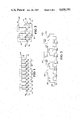
- FIG. 1 is a schematic diagram of cascaded inverters in accordance with a preferred embodiment of the present invention.
- FIG. 2 shows a circuit which uses a switch to vary propagation time through the circuit.
- FIG. 3 shows a circuit which varies propagation delay from an input to an output by means of switches organized in the form of a binary tree.
- FIG. 4 shows a circuit which varies propagation delay by means of an analog signal.
- FIGS. 5A-5B show the coupling of two inverters to form a delay stage.
- FIGS. 5C-5E show the coupling of two inverters to form a delay stage in accordance with preferred embodiments of the present invention.
- Delay of a binary signal may be accomplished by coupling the signal througha series of saturating elements. What is meant by a binary signal is a signal which changes between two voltage levels.
- the voltage levels, commonly referred to as logic 0 and logic 1 may be, for example, 0 volts and 3 volts.
- a binary signal (Vb 1 ) is applied to an input 12 of a plurality of cascaded saturating circuit elements, in this case inverters 14, 16, 18, 20, 22, 24, 26, 28, and 30.
- a supply voltage (Vdd), for example 3 volts, is coupled to the system at a node 32.
- each of the plurality of cascaded inverters has a propagation (or delay) time t of a few (e.g. 3-20) nanoseconds.
- the delay of the binary signal is equal to the number of inverters multiplied by the propagation time through each inverter. In the circuit of FIG. 1, this equals 9t.
- a binary signal (Vb 2 ) is coupled at an input 46 to a plurality of cascaded inverters 34, 36, and 38.
- An output 42 is coupled toa node 50 or a node 48.
- a single-pole-double-throw switch 44 or its logic equivalent toggles output 42 between node 50 and node 48, and thus varies the duration of delay from input 46 to output 42. For example, if each of the cascaded inverters has a propagation time t, the delay when output 42 is coupled to node 48 is t and the delay when output 42 is coupled to node50 is 3t.
- FIG. 3 an example is shown of a means to vary delay propagation by digital switching utilizing a binary tree.
- a binary signal is coupled at an input 320 to a plurality of delay elements 321, 322, 323, 324, 325, 326, and 327, typically groups of cascaded inverters as in FIGS. 1 and 2.
- delay time T will be the same for each delay element group 321-327.
- a series of logic switches 331, 332, 333, 334, 341, 342, and 351 which are typically single-pole-double-throw switches or their logic equivalent, are arranged in the form of a binary propagation time through the entire circuit.
- switches 331-334, 341-342, and 351 the range of propagation delay from input 320 to an output 360 is 0T to 7T.
- switch 351 forms the first level
- switches 341 and 342 form the second level
- switches 331,332, 333, and 334 form the third order level.
- the switches at each level for convenience, may be switched together.
- third level switches 331, 332, 333, and 334 are each selecting a pole labeled "1".
- each level of switches represents a bit in a binary number.
- Level 1 is the most significant bit
- level 2 is the next most significant bit
- level 3 is the least significant bit
- level 1 switch 351 is set at "1”
- level 2 switches 341-342 are set at "0”
- level 3 switches 331-334 are set at "1” so that the current delay is 101 base 2 times T, that is 5T.
- a binary signal (Vb 4 ) is coupled at an input 72 to a plurality of saturating elements, 64, 66, 68, and 70, typically cascaded inverters, as shown.
- Variable resistors 74, 76, 78, and 80 for example depletion-type metal-oxide-silicon field effect transistors (MOSFETS), are controlled by a voltage (Vc 4 ) applied to an input 62 and function as variable current sources.
- Vc 4 voltage
- delay time t varies as Vc 4 varies, typically, when Vc 4 is held constant, delay time t will be the same for each saturating element 64, 66, 68, and 70, when saturating elements 64, 66, 68, and 70 are fabricated on a single integrated circuit. Delay from input 72 to output 60, therefore, is always 4t.
- Vc 4 is decreased, resistance across each of variable resistors 74, 76, 78, and 80increases, decreasing current through variable resistors 74, 76, 78, and 80and thereby increasing the propagation (delay) time t of each of the saturating elements 64, 66, 68, and 70.
- propagation time t decreases. Therefore, varying Vc 4 varies the delay from input 72 to output 60.
- FIGS. 5A-5E illustrate the coupling of two inverters on an integrated circuit.
- FIG. 5A shows a circuit where an inverter 607, comprising an enhancement-type MOSFET 603 and a depletion-type MOSFET 601, is coupled asshown to an inverter 608, comprising an enhancement-type MOSFET 604 and a depletion-type MOSFET 602.
- MOSFETs 601 and 602 act as load resistances forinverters 607 and 608.
- An input node 609 is coupled to an output node of a prior inverter.
- An output node 606 is coupled to an input of a subsequent inverter.
- FIG. 5A shows a circuit where an inverter 607, comprising an enhancement-type MOSFET 603 and a depletion-type MOSFET 601, is coupled asshown to an inverter 608, comprising an enhancement-type MOSFET 604 and a depletion-type MOSFET 602.
- signal Vo on output 606 is the sameas a voltage Vi on input 609 after a propagation delay through inverter 607and a propagation dely through inverter 608.
- a ratio of rise to fall time was at least 3:1.
- rise time is the time it takes for signal Vo to rise from logic 0to logic 1 after signal Vo starts to rise from logic 0 to logic 1.
- fall time is the time it takes for signal Vo to fall from logic 1to logic 0 after signal Vo starts its fall from logic 1 to logic 0.
- an inverter 631 comprising an enhancement-type MOSFET 623 and adepletion-type MOSFET 621
- an inverter 632 comprising an enhancement-type MOSFET 624 and a depletion-type MOSFET 622.
- MOSFETs 621 and 622 act as variable load resistances.
- An input node 629 andan input node 627 are coupled to output nodes of a prior inverter.
- An output node 626 and an output node 634 are coupled to inputs of a subsequent inverter.
- input 629 is coupled to MOSFET 623, and is also coupled to a gate 628 of MOSFET 622.
- a node 625of inverter 631 is coupled to MOSFET 624 at a gate 630, and is also coupledto output node 626.
- the rise to fall ratio from input 629 to output 634 forthe circuit of FIG. 5B was found to be about 1.5:1. This characteristic makes the circuit in FIG. 5B better qualified than the circuit in FIG. 5A to propagate high frequency pulse trains.
- FIG. 5C shows a circuit where two inverters, 114 and 116 are coupled. Varying a voltage Vc 5 applied to an input 118 varies resistance across a depletion-type MOSFET 102 and a depletion-type MOSFET 104 which both function as variable current sources An input node 98 and an input node 100 are coupled to outputs nodes of a prior inverter. A voltage V 100 on input node 100 is an inverse of a voltage v 98 on input node 98, i.e., when v 98 is at logic 1, then V 100 is logic 0, andvice-versa.
- a depletion-type MOSFET 106 and an enhancement-type MOSFET 110 of inverter 114 are coupled as shown to a depletion-type MOSFET 108 and an enhancement-type MOSFET 112 of inverter 116.
- An output node 94 and an output node 96 are then available to be coupled to a succeeding inverter.
- MOSFETs 102 and 104 The major difference between the circuit in FIG. 5B and the circuit in FIG.5C is the addition of MOSFETs 102 and 104. These MOSFETs were added in inverters 114 and 116, and similar MOSFETs may be added to every inverter in a series of cascaded inverters, to vary the delay time across each inverter by controlling the current through the inverters. This capacity to vary delay time can be used to standardize propagation time between integrated circuits. Propagation time through integrated circuits may varybecause of process variations in the process used to fabricate the integrated circuit. Process variations may include variations in doping density for depletion mode load devices, variations in gate geometries forsmall geometry devices, and environmental variations, such as variations intemperature.
- FIGS. 5D and 5E illustrate alternative embodiments for coupling inverters. These embodiments allow for compensation for for wide variation in propagation time resulting from process variations, without impingement onother inverter performance parameters.
- each inverter 355 and 356 has two depletion-type MOSFETS--MOSFETS 351 and 353 in inverter 355, and MOSFETs 352 and 354 in inverter 356--coupled in series to provide time delay variation through current control.
- FIG. 5D each inverter 355 and 356has two depletion-type MOSFETS--MOSFETS 351 and 353 in inverter 355, and MOSFETs 352 and 354 in inverter 356--coupled in series to provide time delay variation through current control.
- each inverter 385 and 386 has one depletion-type MOSFET 381 and an enhancement-type MOSFET--a depletion-type MOSFET 381 and an enhancement-type MOSFET 383 in inverter 385 and a depletion-type MOSFET 382 and an enhancement-type MOSFET 384 in inverter 386--coupled in parallel to provide time delay variance through current control.
Abstract
Description
Claims (13)
Priority Applications (6)
| Application Number | Priority Date | Filing Date | Title |
|---|---|---|---|
| US06/628,069 US4638191A (en) | 1984-07-05 | 1984-07-05 | Amplitude insensitive delay line |
| EP19850108223 EP0167157B1 (en) | 1984-07-05 | 1985-07-04 | Delay circuit |
| DE8585108223T DE3585706D1 (en) | 1984-07-05 | 1985-07-04 | DELAY CIRCUIT. |
| JP60149096A JP2639390B2 (en) | 1984-07-05 | 1985-07-05 | Delay circuit |
| US06/902,995 US4703251A (en) | 1984-07-05 | 1986-09-02 | Testing and calibrating of amplitude insensitive delay lines |
| HK54593A HK54593A (en) | 1984-07-05 | 1993-06-03 | Delay circuit |
Applications Claiming Priority (1)
| Application Number | Priority Date | Filing Date | Title |
|---|---|---|---|
| US06/628,069 US4638191A (en) | 1984-07-05 | 1984-07-05 | Amplitude insensitive delay line |
Related Child Applications (1)
| Application Number | Title | Priority Date | Filing Date |
|---|---|---|---|
| US06/902,995 Division US4703251A (en) | 1984-07-05 | 1986-09-02 | Testing and calibrating of amplitude insensitive delay lines |
Publications (1)
| Publication Number | Publication Date |
|---|---|
| US4638191A true US4638191A (en) | 1987-01-20 |
Family
ID=24517323
Family Applications (1)
| Application Number | Title | Priority Date | Filing Date |
|---|---|---|---|
| US06/628,069 Expired - Lifetime US4638191A (en) | 1984-07-05 | 1984-07-05 | Amplitude insensitive delay line |
Country Status (2)
| Country | Link |
|---|---|
| US (1) | US4638191A (en) |
| JP (1) | JP2639390B2 (en) |
Cited By (7)
| Publication number | Priority date | Publication date | Assignee | Title |
|---|---|---|---|---|
| US4797585A (en) * | 1986-03-31 | 1989-01-10 | Mitsubishi Denki Kabushiki Kaisha | Pulse generating circuit in a semiconductor integrated circuit and a delay circuit therefor |
| US5214320A (en) * | 1992-06-12 | 1993-05-25 | Smos Systems, Inc. | System and method for reducing ground bounce in integrated circuit output buffers |
| US5243227A (en) * | 1991-11-01 | 1993-09-07 | Hewlett-Packard Company | Fine/coarse wired-or tapped delay line |
| US5283631A (en) * | 1991-11-01 | 1994-02-01 | Hewlett-Packard Co. | Programmable capacitance delay element having inverters controlled by adjustable voltage to offset temperature and voltage supply variations |
| US5734680A (en) * | 1995-08-09 | 1998-03-31 | Hewlett-Packard Co. | Analog implementation of a partial response maximum likelihood (PRML) read channel |
| US20050052255A1 (en) * | 2003-09-05 | 2005-03-10 | Infinera Corporation | Transmission line with low dispersive properties and its application in equalization |
| US20070096848A1 (en) * | 2005-10-31 | 2007-05-03 | Larson Thane M | Tunable delay line |
Citations (13)
| Publication number | Priority date | Publication date | Assignee | Title |
|---|---|---|---|---|
| US3553484A (en) * | 1967-03-15 | 1971-01-05 | Int Standard Electric Corp | Pulse generator with time delay |
| US3760280A (en) * | 1972-06-07 | 1973-09-18 | Taft Broadcasting Corp | Method and apparatus for delaying an electrical signal |
| US3973138A (en) * | 1975-05-05 | 1976-08-03 | General Electric Company | Bucket brigade transversal filter |
| US4011402A (en) * | 1973-08-24 | 1977-03-08 | Hitachi, Ltd. | Scanning circuit to deliver train of pulses shifted by a constant delay one after another |
| US4124820A (en) * | 1975-10-01 | 1978-11-07 | American Videonetics Corporation | Asynchronous digital delay line |
| US4408168A (en) * | 1979-11-29 | 1983-10-04 | Fujitsu Limited | Delay circuit oscillator having unequal on and off times |
| US4473762A (en) * | 1980-10-22 | 1984-09-25 | Tokyo Shibaura Denki Kabushiki Kaisha | Semiconductor integrated circuit with a response time compensated with respect to temperature |
| US4489342A (en) * | 1981-03-06 | 1984-12-18 | Itt Industries, Inc. | MOSFET Integrated delay circuit for digital signals and its use in color-televison receivers |
| US4491747A (en) * | 1981-09-30 | 1985-01-01 | Tokyo Shibaura Denki Kabushiki Kaisha | Logic circuit using depletion mode field effect switching transistors |
| US4494021A (en) * | 1982-08-30 | 1985-01-15 | Xerox Corporation | Self-calibrated clock and timing signal generator for MOS/VLSI circuitry |
| US4503341A (en) * | 1983-08-31 | 1985-03-05 | Texas Instruments Incorporated | Power-down inverter circuit |
| US4535259A (en) * | 1982-06-18 | 1985-08-13 | Seeq Technology, Inc. | Sense amplifier for use with a semiconductor memory array |
| US4593203A (en) * | 1982-02-10 | 1986-06-03 | Tokyo Shibaura Denki Kabushiki Kaisha | Semiconductor integrated circuit which allows adjustment of circuit characteristics in accordance with storage data of nonvolatile memory element |
Family Cites Families (1)
| Publication number | Priority date | Publication date | Assignee | Title |
|---|---|---|---|---|
| JPS5254358A (en) * | 1975-10-30 | 1977-05-02 | Fujitsu Ltd | Delay circuit |
-
1984
- 1984-07-05 US US06/628,069 patent/US4638191A/en not_active Expired - Lifetime
-
1985
- 1985-07-05 JP JP60149096A patent/JP2639390B2/en not_active Expired - Lifetime
Patent Citations (13)
| Publication number | Priority date | Publication date | Assignee | Title |
|---|---|---|---|---|
| US3553484A (en) * | 1967-03-15 | 1971-01-05 | Int Standard Electric Corp | Pulse generator with time delay |
| US3760280A (en) * | 1972-06-07 | 1973-09-18 | Taft Broadcasting Corp | Method and apparatus for delaying an electrical signal |
| US4011402A (en) * | 1973-08-24 | 1977-03-08 | Hitachi, Ltd. | Scanning circuit to deliver train of pulses shifted by a constant delay one after another |
| US3973138A (en) * | 1975-05-05 | 1976-08-03 | General Electric Company | Bucket brigade transversal filter |
| US4124820A (en) * | 1975-10-01 | 1978-11-07 | American Videonetics Corporation | Asynchronous digital delay line |
| US4408168A (en) * | 1979-11-29 | 1983-10-04 | Fujitsu Limited | Delay circuit oscillator having unequal on and off times |
| US4473762A (en) * | 1980-10-22 | 1984-09-25 | Tokyo Shibaura Denki Kabushiki Kaisha | Semiconductor integrated circuit with a response time compensated with respect to temperature |
| US4489342A (en) * | 1981-03-06 | 1984-12-18 | Itt Industries, Inc. | MOSFET Integrated delay circuit for digital signals and its use in color-televison receivers |
| US4491747A (en) * | 1981-09-30 | 1985-01-01 | Tokyo Shibaura Denki Kabushiki Kaisha | Logic circuit using depletion mode field effect switching transistors |
| US4593203A (en) * | 1982-02-10 | 1986-06-03 | Tokyo Shibaura Denki Kabushiki Kaisha | Semiconductor integrated circuit which allows adjustment of circuit characteristics in accordance with storage data of nonvolatile memory element |
| US4535259A (en) * | 1982-06-18 | 1985-08-13 | Seeq Technology, Inc. | Sense amplifier for use with a semiconductor memory array |
| US4494021A (en) * | 1982-08-30 | 1985-01-15 | Xerox Corporation | Self-calibrated clock and timing signal generator for MOS/VLSI circuitry |
| US4503341A (en) * | 1983-08-31 | 1985-03-05 | Texas Instruments Incorporated | Power-down inverter circuit |
Non-Patent Citations (14)
| Title |
|---|
| A Novel Precision MOS Synchronous Delay Line by Mel Bazes, IEEE Journal of Solid State Circuits, vol. SC 20, No. 6, Dec. 1985. * |
| A Novel Precision MOS Synchronous Delay Line by Mel Bazes, IEEE Journal of Solid-State Circuits, vol. SC-20, No. 6, Dec. 1985. |
| Electronics Engineers Handbook by Fink McGraw Hill Book Co., copyright 1982, pp. 16 16. * |
| Electronics Engineers' Handbook by Fink McGraw-Hill Book Co., copyright 1982, pp. 16-16. |
| H. Edward Karrer & Arthur M. Dickey, "Ultrasound Imaging: an Overview", Hewlett-Packard Journal, Oct. 1983, pp. 3-6. |
| H. Edward Karrer & Arthur M. Dickey, Ultrasound Imaging: an Overview , Hewlett Packard Journal, Oct. 1983, pp. 3 6. * |
| Heinz E. Kallmann, "Transversal Filters", Proceedings of the I.R.E., Jul. 1940, pp. 302-310. |
| Heinz E. Kallmann, Transversal Filters , Proceedings of the I.R.E., Jul. 1940, pp. 302 310. * |
| Jonathan Taft, "A Digital Delay Line, Implemented in VLSI", abstract of talk given at MIT in Mar./Apr., 1983. |
| Jonathan Taft, A Digital Delay Line, Implemented in VLSI , abstract of talk given at MIT in Mar./Apr., 1983. * |
| Joseph F. Lutz, Synchronous Relay Line Detector Provides Wideband Performance, Microwaves & RF, Nov. 1982, 71, 74, 75, 79. * |
| Joseph F. Lutz, Synchronous Relay-Line Detector Provides Wideband Performance, Microwaves & RF, Nov. 1982, 71, 74, 75, 79. |
| Phillip K. Hardage and Stephen W. Peurifoy, "Method and Apparatus for Delaying a Pulse", s/n 352,671, filed 2/26/82, Abandoned U.S. Patent Application. |
| Phillip K. Hardage and Stephen W. Peurifoy, Method and Apparatus for Delaying a Pulse , s/n 352,671, filed 2/26/82, Abandoned U.S. Patent Application. * |
Cited By (9)
| Publication number | Priority date | Publication date | Assignee | Title |
|---|---|---|---|---|
| US4797585A (en) * | 1986-03-31 | 1989-01-10 | Mitsubishi Denki Kabushiki Kaisha | Pulse generating circuit in a semiconductor integrated circuit and a delay circuit therefor |
| US5243227A (en) * | 1991-11-01 | 1993-09-07 | Hewlett-Packard Company | Fine/coarse wired-or tapped delay line |
| US5283631A (en) * | 1991-11-01 | 1994-02-01 | Hewlett-Packard Co. | Programmable capacitance delay element having inverters controlled by adjustable voltage to offset temperature and voltage supply variations |
| US5214320A (en) * | 1992-06-12 | 1993-05-25 | Smos Systems, Inc. | System and method for reducing ground bounce in integrated circuit output buffers |
| US5734680A (en) * | 1995-08-09 | 1998-03-31 | Hewlett-Packard Co. | Analog implementation of a partial response maximum likelihood (PRML) read channel |
| US20050052255A1 (en) * | 2003-09-05 | 2005-03-10 | Infinera Corporation | Transmission line with low dispersive properties and its application in equalization |
| US7446622B2 (en) | 2003-09-05 | 2008-11-04 | Infinera Corporation | Transmission line with low dispersive properties and its application in equalization |
| US20070096848A1 (en) * | 2005-10-31 | 2007-05-03 | Larson Thane M | Tunable delay line |
| US7332983B2 (en) | 2005-10-31 | 2008-02-19 | Hewlett-Packard Development Company, L.P. | Tunable delay line using selectively connected grounding means |
Also Published As
| Publication number | Publication date |
|---|---|
| JP2639390B2 (en) | 1997-08-13 |
| JPS6143811A (en) | 1986-03-03 |
Similar Documents
| Publication | Publication Date | Title |
|---|---|---|
| US5374860A (en) | Multi-tap digital delay line | |
| US4899071A (en) | Active delay line circuit | |
| US4703251A (en) | Testing and calibrating of amplitude insensitive delay lines | |
| US4988960A (en) | FM demodulation device and FM modulation device employing a CMOS signal delay device | |
| US5808498A (en) | At frequency phase shifting circuit for use in a quadrature clock generator | |
| DE10161054B4 (en) | Clock and data recovery circuit and clock control method | |
| US5229668A (en) | Method and apparatus for high speed digital sampling of a data signal | |
| US3997973A (en) | Transversal frequency filter | |
| EP0315376B1 (en) | Adjustable delay element for digital systems | |
| GB2070855A (en) | Ccd arrangements | |
| US5105108A (en) | Delay circuit with phase locked loop control | |
| US6169436B1 (en) | Variable delay circuit | |
| US4638191A (en) | Amplitude insensitive delay line | |
| US4658225A (en) | Amplitude insensitive delay lines in a transversal filter | |
| US4603301A (en) | Amplitude insensitive delay lines in a frequency modulated signal detector | |
| US4420743A (en) | Voltage comparator using unequal gate width FET's | |
| JPS5972814A (en) | Delay circuit | |
| US4633308A (en) | Amplitude insensitive delay lines in an accoustic imaging system | |
| JPH1127116A (en) | Semiconductor integrated circuit, voltage controlled delay line, delay locked loop, self-synchronous pipeline digital system, voltage controlled oscillator and phase-locked loop | |
| US4593266A (en) | Analog-to-digital converter/demodulator for FM signals | |
| US5132993A (en) | Shift register circuit | |
| US5600273A (en) | Constant delay logic circuits and methods | |
| US4598217A (en) | High speed phase/frequency detector | |
| US4691170A (en) | Frequency multiplier circuit | |
| US5121015A (en) | Voltage controlled delay element |
Legal Events
| Date | Code | Title | Description |
|---|---|---|---|
| AS | Assignment |
Owner name: HEWLETT-PACKARD COMPANY, PALO ALTO, CA A CORP OF C Free format text: ASSIGNMENT OF ASSIGNORS INTEREST.;ASSIGNORS:BAUMGARTNER, RICHARD A.;DUKES, JOHN N.;FISHER, GEORGE A.;REEL/FRAME:004284/0748;SIGNING DATES FROM 19840523 TO 19840625 |
|
| STCF | Information on status: patent grant |
Free format text: PATENTED CASE |
|
| FEPP | Fee payment procedure |
Free format text: PAYOR NUMBER ASSIGNED (ORIGINAL EVENT CODE: ASPN); ENTITY STATUS OF PATENT OWNER: LARGE ENTITY |
|
| FPAY | Fee payment |
Year of fee payment: 4 |
|
| FPAY | Fee payment |
Year of fee payment: 8 |
|
| FPAY | Fee payment |
Year of fee payment: 12 |
|
| AS | Assignment |
Owner name: HEWLETT-PACKARD COMPANY, A DELAWARE CORPORATION, C Free format text: MERGER;ASSIGNOR:HEWLETT-PACKARD COMPANY, A CALIFORNIA CORPORATION;REEL/FRAME:010841/0649 Effective date: 19980520 |
|
| AS | Assignment |
Owner name: AGILENT TECHNOLOGIES INC., CALIFORNIA Free format text: ASSIGNMENT OF ASSIGNORS INTEREST;ASSIGNOR:HEWLETT-PACKARD COMPANY, A DELAWARE CORPORATION;REEL/FRAME:010901/0336 Effective date: 20000520 |