US3881884A - Method for the formation of corrosion resistant electronic interconnections - Google Patents
Method for the formation of corrosion resistant electronic interconnections Download PDFInfo
- Publication number
- US3881884A US3881884A US406125A US40612573A US3881884A US 3881884 A US3881884 A US 3881884A US 406125 A US406125 A US 406125A US 40612573 A US40612573 A US 40612573A US 3881884 A US3881884 A US 3881884A
- Authority
- US
- United States
- Prior art keywords
- film
- accordance
- composite
- chromium
- gold
- Prior art date
- Legal status (The legal status is an assumption and is not a legal conclusion. Google has not performed a legal analysis and makes no representation as to the accuracy of the status listed.)
- Expired - Lifetime
Links
Images
Classifications
-
- H—ELECTRICITY
- H05—ELECTRIC TECHNIQUES NOT OTHERWISE PROVIDED FOR
- H05K—PRINTED CIRCUITS; CASINGS OR CONSTRUCTIONAL DETAILS OF ELECTRIC APPARATUS; MANUFACTURE OF ASSEMBLAGES OF ELECTRICAL COMPONENTS
- H05K3/00—Apparatus or processes for manufacturing printed circuits
- H05K3/22—Secondary treatment of printed circuits
- H05K3/24—Reinforcing the conductive pattern
- H05K3/244—Finish plating of conductors, especially of copper conductors, e.g. for pads or lands
-
- H—ELECTRICITY
- H01—ELECTRIC ELEMENTS
- H01B—CABLES; CONDUCTORS; INSULATORS; SELECTION OF MATERIALS FOR THEIR CONDUCTIVE, INSULATING OR DIELECTRIC PROPERTIES
- H01B1/00—Conductors or conductive bodies characterised by the conductive materials; Selection of materials as conductors
-
- H—ELECTRICITY
- H05—ELECTRIC TECHNIQUES NOT OTHERWISE PROVIDED FOR
- H05K—PRINTED CIRCUITS; CASINGS OR CONSTRUCTIONAL DETAILS OF ELECTRIC APPARATUS; MANUFACTURE OF ASSEMBLAGES OF ELECTRICAL COMPONENTS
- H05K3/00—Apparatus or processes for manufacturing printed circuits
- H05K3/38—Improvement of the adhesion between the insulating substrate and the metal
- H05K3/388—Improvement of the adhesion between the insulating substrate and the metal by the use of a metallic or inorganic thin film adhesion layer
-
- H10P95/00—
-
- H10W20/425—
-
- H10W20/4432—
-
- H10W72/012—
-
- H—ELECTRICITY
- H05—ELECTRIC TECHNIQUES NOT OTHERWISE PROVIDED FOR
- H05K—PRINTED CIRCUITS; CASINGS OR CONSTRUCTIONAL DETAILS OF ELECTRIC APPARATUS; MANUFACTURE OF ASSEMBLAGES OF ELECTRICAL COMPONENTS
- H05K2203/00—Indexing scheme relating to apparatus or processes for manufacturing printed circuits covered by H05K3/00
- H05K2203/11—Treatments characterised by their effect, e.g. heating, cooling, roughening
- H05K2203/1105—Heating or thermal processing not related to soldering, firing, curing or laminating, e.g. for shaping the substrate or during finish plating
-
- H10W72/251—
-
- H10W72/923—
-
- H10W72/952—
Definitions
- ABSTRACT Disclosed is a method for the manufacture of composite thin films useful among other applications as electronic microcircuit interconnections, fuses, and contacts, terminal pads and voltage distribution ring metallurgy comprising in carrying out an integral circuit fabrication process the steps of first depositing a barrier layer of antidiffusion material, such as chromium, followed by superimposing thereon a film of highly conductive metals susceptible to corrosion and followed by the deposition of a highly corrosive resistant metal film. A subtractive etch pattern is formed in the composite metal film followed by heating the structure to an elevated temperature for a predetermined period of time so that the uppermost layer of the composite flows by diffusion over the edge section to protect the conductive metal film from corrosive effects.
- a barrier layer of antidiffusion material such as chromium
- microminiaturized circuitry A major problem in the manufacture of highly miniaturized electronic circuitry, also referred to as microminiaturized circuitry, has been the interconnection of the various elements or subcircuits comprising the circuits. Because of the extremely small size of the components and even smaller of the electrical leads used with such components, the use of conventional wiring techniques is so inefficient as to be completely impractica].
- printed circuit terminations in which connecting copper tubes are coated with a layer of a noble metal such as gold
- the coating of gold is suitable for forming thermal compression bonds or welds with a copper base because the coating of gold is capable of plastic flow and diffusion which promotes thermal compression welding to form true metallurgical bonds.
- printed circuits by a technique comprising an electrically conductive circuit portion consisting of a base metal of copper alloy with a first layer thereon of a noble metal selected from a group consisting of platinum, rhodium, palladium, and ruthenium and a layer of gold on the top of the first metal layer.
- One other contact termination or path that has been utilized comprises successive layers of nickel-chromium alloy. copper and palladium. Copper by itself does not adhere strongly to silicon or certain other materials such as semiconductor materials used in the manufacture of thin film circuitry. Therefore, prior art teachings revealed a nickel-chromium alloy layer as a suitable material which will readily adhere to both the thin film circuit and the superimposed copper layer. Copper is used as a layer because of its good solderability as well as good electrical conductivity characteristics. These properties decrease the overall resistivity of the termination particularly at the junction with a solder.
- thin films be stable, firmly adherent and otherwise resistant to a variety of mechanical, chemical, thermal and electrical stresses.
- conductor lines of the multilayer structure are tinned and then transistor or other elements are soldered thereto.
- vacuum deposited chromium is used as a primer or underlayer for copper conductor lines for improving the adherence of the copper to the dielectric which is typically silicon dioxide, quartz or even an organic polymer.
- the high energy deposition e.g. sputtering, of chromium and other barrier layers thereon tends all the more to aggrevate the problem of insulation breakdown at cross overs.
- any processing improvement for reduction of cross over insulation failure must take into account the delicate nature of the structures involved and the requirement that the inter-adherence on the superimposed layers must not be diminished.
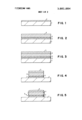
- FIG. 1 is a cross-sectional view illustrating a substrate having the first metal layer of the composite thereon.
- FIG. 2 is a similar cross-sectional view as FIG. 1 showing an intermediate transitional metal layer and the second metal layer of the composite deposition.
- FIG. 3 is a similar cross-sectional view as FIG. 2 having the final metal layer of the composite deposited thereon.
- FIG. 4 is a similar cross-sectional view as FIG. 3 illustrating the subtractive etch of a portion of the composite shown in FIG. 3.
- FIG. 5 is a similar cross-sectional view as FIG. 4 illustrating the final step in the process subsequent to the heating step.
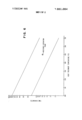
- FIG. 6 is a plot of the heating or annealing step conditions showing time versus temperature.
- contact conductive metallurgy in association with the passivating material is dependent upon the relationship between the modulus of elasticity and thermal expansion coefficients of the materials to be used.
- the proper selection of these materials with regard to their physical characteristics minimizes or avoids thermal stressing resulting from heat treatment and annealing during subsequent processing steps, as well as under ultimate operating conditions. Thermally induced stresses cause cracking and other defects in the materials which result in shorting or other electrical malfunctions which in turn makes the ultimate device inoperative or defective.
- FIG. 1 illustrates a substrate l of any desired passivating material. such as quartz. organic polyimide or any other materials. and having deposited thereon a first film of chromium 2.
- Film deposition is accomplished by any well known techniques such as evaporative deposition. chemical vapor deposition methods, sputtering, and the like.
- the first or primary film deposited acts as a diffusion barrier and adhesion promotor upon which subsequent conductive films are formed to make a composite structure.
- a quartz substrate having previously formed device structures at lower levels and being from l0.000 to 50,000 Angstroms in thickness was subjected to a first chromium deposition by the known evaporative technique wherein a metal source is heated to evaporation conditions and the metal deposited in a controlled manner on the structure. If a multiplicity of devices are formed on a single substrate. the entire substrate can receive the first barrier layer simultaneously.
- a layer of chromium from 650 Angstroms to 750 Angstroms was deposited at the rate of approximately 4 Angstroms per second under an evaporative substrate temperature between C and 165C.
- the thickness of the film to be deposited is dependent upon the ultimate device structure and usage as well as the nature of the physical properties of the substrate and the relative coefficients of expansion values of the film metal and the substrate material. In this instance, a film of 700 Angstroms of chromium was deposited upon quartz.
- FIG. 2 illustrates the structure of FIG. I upon which an intermediate layer of chromium and copper 3 was deposited by continuing the evaporative deposition of chromium and adding thereto copper from a separate evaporation source so that a mixture or two phase structure of chromium and copper is deposited upon the first deposited chromium layer.
- the source of copper and chromium may be possibly accomplished from a single evaporative source of the desired transitory film mixture per se. This technique allows an inte gral transition between the two metals insuring adequate bonding.
- 500 Angstroms of chromium-copper was deposited at a rate of between 6 to 10 Angstroms per second at a temperature of C in the preferred deposition range of I35C to C.
- the chromium source was terminated and the copper deposition continued at a rate of between 12 to 16 Angstroms per second to a copper layer thickness of 9,000 Angstroms illustrated at 4 in FIG. 2 whereupon the copper source is terminated and a gold deposition source activated to produce the upper most layer of gold as illustrated at 5 in FIG. 3.
- Gold deposition was carried out at a rate of between 5 to 7 Angstroms per second at a deposition temperature of I50C until a thickness of L400 Angstroms was acquired.
- the preferred structure comprises 650 to 750 Angstroms of first layer chromium. 450 to 550 Angstroms of transitory chromium-copper layer. 8,500 to 9,500 Angstroms of copper. and an uppermost layer of L250 to 1,550 Angstroms of gold producing a composite structure as illustrated in FIG. 3.
- FIG. 3 Utilizing well known standard photolithography techniques, the structure illustrated in FIG. 3 was appropriately masked and subtractively etched using an etchant process comprising a double bath of potassium iodideiodine (KI-I followed by KMnO, in caustic solution to form a structure as illustrated in FIG. 4 wherein the edges or sides of the composite layer previously formed are exposed as illustrated by the reference numerals 2, 3, 4 and S of FIG. 4.
- an etchant process comprising a double bath of potassium iodideiodine (KI-I followed by KMnO, in caustic solution to form a structure as illustrated in FIG. 4 wherein the edges or sides of the composite layer previously formed are exposed as illustrated by the reference numerals 2, 3, 4 and S of FIG. 4.
- the subtractively etched structure illustrated in FIG. 4 is subjected to heat treatment in an inert gas atmosphere such as nitrogen or argon or other desired atmosphere t'or example a hydrogen reducing ambient for a period of time and temperature illustrated in the plot of FIG. 6 and within the maximum and minimum limits therein delineated.
- an inert gas atmosphere such as nitrogen or argon or other desired atmosphere t'or example a hydrogen reducing ambient
- a chromium-coppcr-gold composite is formed on a quartz substrate a preferred heat treatment or annealing temperature of 350C and the corresponding time period is desirable while main taining an atmosphere of hydrogen.
- a preferred heat treatment or annealing temperature 350C and the corresponding time period is desirable while main taining an atmosphere of hydrogen.
- these heat treatment conditions are dependent upon substrate material.
- metallurgy composition, thickness and corresponding physical and chemical properties of the substances and that this specific embodiment is only illustrative of the invention.
- metal film disposition temperature is between
- the thicknesses of the substrate layer and the various metal layers of the composite conductive materials may be varied in accordance with the physical and chemical properties of the substrate and the deposited metallurgy with particular reference to the modulus of elasticity and the coefficient of expansion of these materials.
- FIG. depicts a composite conductive layer.
- the top and side exposed surfaces covered with a noncorrosive metal or alloy suitable for use in miniaturized electronic integrated circuits.
- a noncorrosive metal or alloy suitable for use in miniaturized electronic integrated circuits.
- noble metals such as gold. platinum, palladium, iriduim, rhodium, ruthenium and 0s mium.
Landscapes
- Engineering & Computer Science (AREA)
- Manufacturing & Machinery (AREA)
- Microelectronics & Electronic Packaging (AREA)
- Chemical & Material Sciences (AREA)
- Inorganic Chemistry (AREA)
- Manufacturing Of Printed Wiring (AREA)
- Electrodes Of Semiconductors (AREA)
- Parts Printed On Printed Circuit Boards (AREA)
- Internal Circuitry In Semiconductor Integrated Circuit Devices (AREA)
- Production Of Multi-Layered Print Wiring Board (AREA)
- Laminated Bodies (AREA)
- Physical Vapour Deposition (AREA)
Priority Applications (11)
| Application Number | Priority Date | Filing Date | Title |
|---|---|---|---|
| US406125A US3881884A (en) | 1973-10-12 | 1973-10-12 | Method for the formation of corrosion resistant electronic interconnections |
| IT26541/74A IT1020141B (it) | 1973-10-12 | 1974-08-23 | Procedimento per depositare sot tili pellicole in particolare per realizzare interconnessioni in assiemi circuitali microminiaturiz zati |
| DE2440481A DE2440481C3 (de) | 1973-10-12 | 1974-08-23 | Verfahren zum Herstellen von Dünnschicht-Leiterzügen auf einem elektrisch isolierenden Träger |
| FR7430003A FR2247820B1 (OSRAM) | 1973-10-12 | 1974-08-30 | |
| GB4037674A GB1448034A (en) | 1973-10-12 | 1974-09-17 | Corrosion-resistant electrical conductors |
| JP10784874A JPS5310430B2 (OSRAM) | 1973-10-12 | 1974-09-20 | |
| CH1318874A CH569363A5 (OSRAM) | 1973-10-12 | 1974-10-01 | |
| SE7412333A SE401291B (sv) | 1973-10-12 | 1974-10-01 | Metod vid tillverkning av integrerade kretsar for avsettning pa ett delvis bearbetat kretssubstrat av en sammansatt ledande filmstruktur |
| CA210,639A CA1023876A (en) | 1973-10-12 | 1974-10-03 | Method for the formation of corrosion resistant electronic interconnections |
| NL7413310A NL7413310A (nl) | 1973-10-12 | 1974-10-09 | Werkwijze voor de vorming van tegen korrosie ndige elektronische verbindingen en elek- sche verbindingen verkregen met deze werk- |
| BR8490/74A BR7408490D0 (pt) | 1973-10-12 | 1974-10-11 | Processo para fabricar circuitos integrados |
Applications Claiming Priority (1)
| Application Number | Priority Date | Filing Date | Title |
|---|---|---|---|
| US406125A US3881884A (en) | 1973-10-12 | 1973-10-12 | Method for the formation of corrosion resistant electronic interconnections |
Publications (1)
| Publication Number | Publication Date |
|---|---|
| US3881884A true US3881884A (en) | 1975-05-06 |
Family
ID=23606638
Family Applications (1)
| Application Number | Title | Priority Date | Filing Date |
|---|---|---|---|
| US406125A Expired - Lifetime US3881884A (en) | 1973-10-12 | 1973-10-12 | Method for the formation of corrosion resistant electronic interconnections |
Country Status (11)
| Country | Link |
|---|---|
| US (1) | US3881884A (OSRAM) |
| JP (1) | JPS5310430B2 (OSRAM) |
| BR (1) | BR7408490D0 (OSRAM) |
| CA (1) | CA1023876A (OSRAM) |
| CH (1) | CH569363A5 (OSRAM) |
| DE (1) | DE2440481C3 (OSRAM) |
| FR (1) | FR2247820B1 (OSRAM) |
| GB (1) | GB1448034A (OSRAM) |
| IT (1) | IT1020141B (OSRAM) |
| NL (1) | NL7413310A (OSRAM) |
| SE (1) | SE401291B (OSRAM) |
Cited By (32)
| Publication number | Priority date | Publication date | Assignee | Title |
|---|---|---|---|---|
| US4267012A (en) * | 1979-04-30 | 1981-05-12 | Fairchild Camera & Instrument Corp. | Process for patterning metal connections on a semiconductor structure by using a tungsten-titanium etch resistant layer |
| US4290079A (en) * | 1979-06-29 | 1981-09-15 | International Business Machines Corporation | Improved solder interconnection between a semiconductor device and a supporting substrate |
| US4293377A (en) * | 1978-06-29 | 1981-10-06 | Rogers Corporation | Manufacturing method for circuit board |
| US4335506A (en) * | 1980-08-04 | 1982-06-22 | International Business Machines Corporation | Method of forming aluminum/copper alloy conductors |
| US4360142A (en) * | 1979-06-29 | 1982-11-23 | International Business Machines Corporation | Method of forming a solder interconnection capable of sustained high power levels between a semiconductor device and a supporting substrate |
| US4372809A (en) * | 1981-03-02 | 1983-02-08 | Siemens Aktiengesellschaft | Method for manufacturing solderable, temperable, thin film tracks which do not contain precious metal |
| US4386116A (en) * | 1981-12-24 | 1983-05-31 | International Business Machines Corporation | Process for making multilayer integrated circuit substrate |
| US4396900A (en) * | 1982-03-08 | 1983-08-02 | The United States Of America As Represented By The Secretary Of The Navy | Thin film microstrip circuits |
| US4505029A (en) * | 1981-03-23 | 1985-03-19 | General Electric Company | Semiconductor device with built-up low resistance contact |
| US4600600A (en) * | 1983-11-30 | 1986-07-15 | Siemens Aktiengesellschaft | Method for the galvanic manufacture of metallic bump-like lead contacts |
| US4606788A (en) * | 1984-04-12 | 1986-08-19 | Moran Peter L | Methods of and apparatus for forming conductive patterns on a substrate |
| US4711791A (en) * | 1986-08-04 | 1987-12-08 | The Boc Group, Inc. | Method of making a flexible microcircuit |
| US4725877A (en) * | 1986-04-11 | 1988-02-16 | American Telephone And Telegraph Company, At&T Bell Laboratories | Metallized semiconductor device including an interface layer |
| US4851895A (en) * | 1985-05-06 | 1989-07-25 | American Telephone And Telegraph Company, At&T Bell Laboratories | Metallization for integrated devices |
| US5525369A (en) * | 1991-10-17 | 1996-06-11 | International Business Machines Corporation | Method for metallizing through holes in thin film substrates, and resulting devices |
| US6184060B1 (en) | 1996-10-29 | 2001-02-06 | Trusi Technologies Llc | Integrated circuits and methods for their fabrication |
| US6322903B1 (en) | 1999-12-06 | 2001-11-27 | Tru-Si Technologies, Inc. | Package of integrated circuits and vertical integration |
| US20020084513A1 (en) * | 1996-10-29 | 2002-07-04 | Oleg Siniaguine | Integrated circuits and methods for their fabrication |
| US6498074B2 (en) | 1996-10-29 | 2002-12-24 | Tru-Si Technologies, Inc. | Thinning and dicing of semiconductor wafers using dry etch, and obtaining semiconductor chips with rounded bottom edges and corners |
| US20030005582A1 (en) * | 2001-07-05 | 2003-01-09 | Sumitomo Electric Industries, Ltd. | Circuit board, method for manufacturing same, and high-output module |
| US20030186486A1 (en) * | 2002-03-28 | 2003-10-02 | Swan Johanna M. | Integrated circuit die and an electronic assembly having a three-dimensional interconnection scheme |
| US20030183943A1 (en) * | 2002-03-28 | 2003-10-02 | Swan Johanna M. | Integrated circuit die and an electronic assembly having a three-dimensional interconnection scheme |
| US6717254B2 (en) | 2001-02-22 | 2004-04-06 | Tru-Si Technologies, Inc. | Devices having substrates with opening passing through the substrates and conductors in the openings, and methods of manufacture |
| US6753205B2 (en) | 2001-09-13 | 2004-06-22 | Tru-Si Technologies, Inc. | Method for manufacturing a structure comprising a substrate with a cavity and a semiconductor integrated circuit bonded to a contact pad located in the cavity |
| US20040200726A1 (en) * | 2001-11-13 | 2004-10-14 | Lg Electronics Inc. | Method for forming bonding pads |
| US6848177B2 (en) | 2002-03-28 | 2005-02-01 | Intel Corporation | Integrated circuit die and an electronic assembly having a three-dimensional interconnection scheme |
| US20050280153A1 (en) * | 2004-06-17 | 2005-12-22 | Nitto Denko Corporation | Wired circuit forming board, wired circuit board, and thin metal layer forming method |
| US20060270194A1 (en) * | 2005-05-26 | 2006-11-30 | Thompson Vasile R | Semiconductor package and method for forming the same |
| US20140042610A1 (en) * | 2012-08-10 | 2014-02-13 | Cyntec Co., Ltd. | Package structure and the method to fabricate thereof |
| US9741652B1 (en) * | 2016-06-13 | 2017-08-22 | Shinko Electric Industries Co. Ltd. | Wiring substrate |
| CN113133217A (zh) * | 2020-01-15 | 2021-07-16 | 鹏鼎控股(深圳)股份有限公司 | 线路板的制备方法 |
| US20230422393A1 (en) * | 2020-11-27 | 2023-12-28 | Kyocera Corporation | Wiring board |
Families Citing this family (7)
| Publication number | Priority date | Publication date | Assignee | Title |
|---|---|---|---|---|
| DE2834221C3 (de) * | 1978-08-04 | 1981-04-30 | Preh Elektrofeinmechanische Werke Jakob Preh Nachf. GmbH & Co, 8740 Bad Neustadt | Verfahren zur Herstellung von Dünnschichtleiterbahnen |
| JPS5534414A (en) * | 1978-09-01 | 1980-03-11 | Sumitomo Bakelite Co | Method of manufacturing printed circuit board |
| US4319264A (en) | 1979-12-17 | 1982-03-09 | International Business Machines Corporation | Nickel-gold-nickel conductors for solid state devices |
| JPS57141942A (en) * | 1981-02-27 | 1982-09-02 | Fuji Electric Corp Res & Dev Ltd | Formation of bump electrode |
| DE3107857C2 (de) * | 1981-03-02 | 1984-08-23 | Siemens AG, 1000 Berlin und 8000 München | Verfahren zur Herstellung von Dünnfilmschaltungen mit sehr gut lötbaren Leiterbahnschichtsystemen |
| JP2500523B2 (ja) * | 1990-12-28 | 1996-05-29 | 日本電装株式会社 | 基板および基板の製造方法 |
| GB2255672B (en) * | 1991-05-10 | 1994-11-30 | Northern Telecom Ltd | Opto-electronic components |
Citations (3)
| Publication number | Priority date | Publication date | Assignee | Title |
|---|---|---|---|---|
| US2724663A (en) * | 1952-10-23 | 1955-11-22 | Bell Telephone Labor Inc | Plural metal vapor coating |
| US3458925A (en) * | 1966-01-20 | 1969-08-05 | Ibm | Method of forming solder mounds on substrates |
| US3677843A (en) * | 1970-02-02 | 1972-07-18 | Sylvania Electric Prod | Method for fabricating multilayer magnetic devices |
-
1973
- 1973-10-12 US US406125A patent/US3881884A/en not_active Expired - Lifetime
-
1974
- 1974-08-23 DE DE2440481A patent/DE2440481C3/de not_active Expired
- 1974-08-23 IT IT26541/74A patent/IT1020141B/it active
- 1974-08-30 FR FR7430003A patent/FR2247820B1/fr not_active Expired
- 1974-09-17 GB GB4037674A patent/GB1448034A/en not_active Expired
- 1974-09-20 JP JP10784874A patent/JPS5310430B2/ja not_active Expired
- 1974-10-01 CH CH1318874A patent/CH569363A5/xx not_active IP Right Cessation
- 1974-10-01 SE SE7412333A patent/SE401291B/xx unknown
- 1974-10-03 CA CA210,639A patent/CA1023876A/en not_active Expired
- 1974-10-09 NL NL7413310A patent/NL7413310A/xx not_active Application Discontinuation
- 1974-10-11 BR BR8490/74A patent/BR7408490D0/pt unknown
Patent Citations (3)
| Publication number | Priority date | Publication date | Assignee | Title |
|---|---|---|---|---|
| US2724663A (en) * | 1952-10-23 | 1955-11-22 | Bell Telephone Labor Inc | Plural metal vapor coating |
| US3458925A (en) * | 1966-01-20 | 1969-08-05 | Ibm | Method of forming solder mounds on substrates |
| US3677843A (en) * | 1970-02-02 | 1972-07-18 | Sylvania Electric Prod | Method for fabricating multilayer magnetic devices |
Cited By (53)
| Publication number | Priority date | Publication date | Assignee | Title |
|---|---|---|---|---|
| US4293377A (en) * | 1978-06-29 | 1981-10-06 | Rogers Corporation | Manufacturing method for circuit board |
| US4267012A (en) * | 1979-04-30 | 1981-05-12 | Fairchild Camera & Instrument Corp. | Process for patterning metal connections on a semiconductor structure by using a tungsten-titanium etch resistant layer |
| US4290079A (en) * | 1979-06-29 | 1981-09-15 | International Business Machines Corporation | Improved solder interconnection between a semiconductor device and a supporting substrate |
| US4360142A (en) * | 1979-06-29 | 1982-11-23 | International Business Machines Corporation | Method of forming a solder interconnection capable of sustained high power levels between a semiconductor device and a supporting substrate |
| US4335506A (en) * | 1980-08-04 | 1982-06-22 | International Business Machines Corporation | Method of forming aluminum/copper alloy conductors |
| US4372809A (en) * | 1981-03-02 | 1983-02-08 | Siemens Aktiengesellschaft | Method for manufacturing solderable, temperable, thin film tracks which do not contain precious metal |
| US4505029A (en) * | 1981-03-23 | 1985-03-19 | General Electric Company | Semiconductor device with built-up low resistance contact |
| US4386116A (en) * | 1981-12-24 | 1983-05-31 | International Business Machines Corporation | Process for making multilayer integrated circuit substrate |
| US4396900A (en) * | 1982-03-08 | 1983-08-02 | The United States Of America As Represented By The Secretary Of The Navy | Thin film microstrip circuits |
| US4600600A (en) * | 1983-11-30 | 1986-07-15 | Siemens Aktiengesellschaft | Method for the galvanic manufacture of metallic bump-like lead contacts |
| US4606788A (en) * | 1984-04-12 | 1986-08-19 | Moran Peter L | Methods of and apparatus for forming conductive patterns on a substrate |
| US4851895A (en) * | 1985-05-06 | 1989-07-25 | American Telephone And Telegraph Company, At&T Bell Laboratories | Metallization for integrated devices |
| US4725877A (en) * | 1986-04-11 | 1988-02-16 | American Telephone And Telegraph Company, At&T Bell Laboratories | Metallized semiconductor device including an interface layer |
| US4711791A (en) * | 1986-08-04 | 1987-12-08 | The Boc Group, Inc. | Method of making a flexible microcircuit |
| US5525369A (en) * | 1991-10-17 | 1996-06-11 | International Business Machines Corporation | Method for metallizing through holes in thin film substrates, and resulting devices |
| US6740582B2 (en) | 1996-10-29 | 2004-05-25 | Tru-Si Technologies, Inc. | Integrated circuits and methods for their fabrication |
| US6639303B2 (en) | 1996-10-29 | 2003-10-28 | Tru-Si Technolgies, Inc. | Integrated circuits and methods for their fabrication |
| US20020084513A1 (en) * | 1996-10-29 | 2002-07-04 | Oleg Siniaguine | Integrated circuits and methods for their fabrication |
| US6420209B1 (en) | 1996-10-29 | 2002-07-16 | Tru-Si Technologies, Inc. | Integrated circuits and methods for their fabrication |
| US20020127868A1 (en) * | 1996-10-29 | 2002-09-12 | Oleg Siniaguine | Integrated circuits and methods for their fabrication |
| US6498074B2 (en) | 1996-10-29 | 2002-12-24 | Tru-Si Technologies, Inc. | Thinning and dicing of semiconductor wafers using dry etch, and obtaining semiconductor chips with rounded bottom edges and corners |
| US6184060B1 (en) | 1996-10-29 | 2001-02-06 | Trusi Technologies Llc | Integrated circuits and methods for their fabrication |
| US6664129B2 (en) | 1996-10-29 | 2003-12-16 | Tri-Si Technologies, Inc. | Integrated circuits and methods for their fabrication |
| US6322903B1 (en) | 1999-12-06 | 2001-11-27 | Tru-Si Technologies, Inc. | Package of integrated circuits and vertical integration |
| US6717254B2 (en) | 2001-02-22 | 2004-04-06 | Tru-Si Technologies, Inc. | Devices having substrates with opening passing through the substrates and conductors in the openings, and methods of manufacture |
| US20030005582A1 (en) * | 2001-07-05 | 2003-01-09 | Sumitomo Electric Industries, Ltd. | Circuit board, method for manufacturing same, and high-output module |
| US6759599B2 (en) * | 2001-07-05 | 2004-07-06 | Sumitomo Electric Industries, Ltd. | Circuit board, method for manufacturing same, and high-output module |
| US6753205B2 (en) | 2001-09-13 | 2004-06-22 | Tru-Si Technologies, Inc. | Method for manufacturing a structure comprising a substrate with a cavity and a semiconductor integrated circuit bonded to a contact pad located in the cavity |
| US6787916B2 (en) | 2001-09-13 | 2004-09-07 | Tru-Si Technologies, Inc. | Structures having a substrate with a cavity and having an integrated circuit bonded to a contact pad located in the cavity |
| US7257891B2 (en) | 2001-11-13 | 2007-08-21 | Lg Electronics Inc. | Method for forming bonding pads |
| US7304249B2 (en) * | 2001-11-13 | 2007-12-04 | Lg Electronics Inc. | Bonding pads for a printed circuit board |
| US20040200726A1 (en) * | 2001-11-13 | 2004-10-14 | Lg Electronics Inc. | Method for forming bonding pads |
| US20040200638A1 (en) * | 2001-11-13 | 2004-10-14 | Lg Electronic Inc. | Bonding pads for a printed circuit board |
| US20050090042A1 (en) * | 2002-03-28 | 2005-04-28 | Swan Johanna M. | Integrated circuit die and an electronic assembly having a three-dimensional interconnection scheme |
| US20030183943A1 (en) * | 2002-03-28 | 2003-10-02 | Swan Johanna M. | Integrated circuit die and an electronic assembly having a three-dimensional interconnection scheme |
| US6908845B2 (en) | 2002-03-28 | 2005-06-21 | Intel Corporation | Integrated circuit die and an electronic assembly having a three-dimensional interconnection scheme |
| US6848177B2 (en) | 2002-03-28 | 2005-02-01 | Intel Corporation | Integrated circuit die and an electronic assembly having a three-dimensional interconnection scheme |
| US7112887B2 (en) | 2002-03-28 | 2006-09-26 | Intel Corporation | Integrated circuit die and an electronic assembly having a three-dimensional interconnection scheme |
| US20030186486A1 (en) * | 2002-03-28 | 2003-10-02 | Swan Johanna M. | Integrated circuit die and an electronic assembly having a three-dimensional interconnection scheme |
| CN1725933B (zh) * | 2004-06-17 | 2010-10-06 | 日东电工株式会社 | 布线电路形成用基板、布线电路基板以及金属薄层的形成方法 |
| US7417316B2 (en) | 2004-06-17 | 2008-08-26 | Nitto Denko Corporation | Wired circuit forming board, wired circuit board, and thin metal layer forming method |
| EP1608211A3 (en) * | 2004-06-17 | 2007-10-17 | Nitto Denko Corporation | Wired circuit forming board, wired circuit board and thin metal layer forming method |
| US20050280153A1 (en) * | 2004-06-17 | 2005-12-22 | Nitto Denko Corporation | Wired circuit forming board, wired circuit board, and thin metal layer forming method |
| US7339267B2 (en) * | 2005-05-26 | 2008-03-04 | Freescale Semiconductor, Inc. | Semiconductor package and method for forming the same |
| WO2006127107A3 (en) * | 2005-05-26 | 2007-06-14 | Freescale Semiconductor Inc | Semiconductor package and method for forming the same |
| CN100539008C (zh) * | 2005-05-26 | 2009-09-09 | 飞思卡尔半导体公司 | 半导体封装及其形成方法 |
| US20060270194A1 (en) * | 2005-05-26 | 2006-11-30 | Thompson Vasile R | Semiconductor package and method for forming the same |
| US20140042610A1 (en) * | 2012-08-10 | 2014-02-13 | Cyntec Co., Ltd. | Package structure and the method to fabricate thereof |
| US10373930B2 (en) * | 2012-08-10 | 2019-08-06 | Cyntec Co., Ltd | Package structure and the method to fabricate thereof |
| US9741652B1 (en) * | 2016-06-13 | 2017-08-22 | Shinko Electric Industries Co. Ltd. | Wiring substrate |
| CN113133217A (zh) * | 2020-01-15 | 2021-07-16 | 鹏鼎控股(深圳)股份有限公司 | 线路板的制备方法 |
| US20230422393A1 (en) * | 2020-11-27 | 2023-12-28 | Kyocera Corporation | Wiring board |
| US12495486B2 (en) * | 2020-11-27 | 2025-12-09 | Kyocera Corporation | Wiring board |
Also Published As
| Publication number | Publication date |
|---|---|
| BR7408490D0 (pt) | 1975-07-29 |
| CH569363A5 (OSRAM) | 1975-11-14 |
| SE7412333L (OSRAM) | 1975-04-14 |
| IT1020141B (it) | 1977-12-20 |
| NL7413310A (nl) | 1975-04-15 |
| DE2440481C3 (de) | 1978-08-03 |
| JPS5068082A (OSRAM) | 1975-06-07 |
| DE2440481A1 (de) | 1975-04-24 |
| SE401291B (sv) | 1978-04-24 |
| CA1023876A (en) | 1978-01-03 |
| FR2247820A1 (OSRAM) | 1975-05-09 |
| GB1448034A (en) | 1976-09-02 |
| FR2247820B1 (OSRAM) | 1976-10-22 |
| DE2440481B2 (de) | 1977-12-01 |
| JPS5310430B2 (OSRAM) | 1978-04-13 |
Similar Documents
| Publication | Publication Date | Title |
|---|---|---|
| US3881884A (en) | Method for the formation of corrosion resistant electronic interconnections | |
| US3663184A (en) | Solder bump metallization system using a titanium-nickel barrier layer | |
| JP2526007B2 (ja) | 半導体チップへの電気的相互接続を形成するための構造および方法 | |
| US4463059A (en) | Layered metal film structures for LSI chip carriers adapted for solder bonding and wire bonding | |
| US3729820A (en) | Method for manufacturing a package of a semiconductor element | |
| JP6078585B2 (ja) | 小型電子機器、その形成方法、およびシステム | |
| US3290570A (en) | Multilevel expanded metallic contacts for semiconductor devices | |
| JP3062086B2 (ja) | Icパッケージ | |
| US6452271B2 (en) | Interconnect component for a semiconductor die including a ruthenium layer and a method for its fabrication | |
| US4685203A (en) | Hybrid integrated circuit substrate and method of manufacturing the same | |
| US4372809A (en) | Method for manufacturing solderable, temperable, thin film tracks which do not contain precious metal | |
| US2820932A (en) | Contact structure | |
| US3622385A (en) | Method of providing flip-chip devices with solderable connections | |
| US3290565A (en) | Glass enclosed, passivated semiconductor with contact means of alternate layers of chromium, silver and chromium | |
| US3775838A (en) | Integrated circuit package and construction technique | |
| USH498H (en) | Electronic component including soldered electrical leads | |
| US4022931A (en) | Process for making semiconductor device | |
| US5633047A (en) | Electronic devices having metallurgies containing copper-semiconductor compounds | |
| US3436615A (en) | Contact metal system of an allayer adjacent to semi-conductor and a layer of au-al intermetallics adjacent to the conductive metal | |
| JP3089943B2 (ja) | 半導体装置の電極装置 | |
| KR900003472B1 (ko) | 전자부품의 도금방법 | |
| GB2074793A (en) | Thin film circuit assembly | |
| JPH0137876B2 (OSRAM) | ||
| CA1153128A (en) | Electrical circuit assemblies | |
| JP3066201B2 (ja) | 回路基板及びその製造方法 |