US20160079110A1 - Semiconductor package, carrier structure and fabrication method thereof - Google Patents
Semiconductor package, carrier structure and fabrication method thereof Download PDFInfo
- Publication number
- US20160079110A1 US20160079110A1 US14/849,639 US201514849639A US2016079110A1 US 20160079110 A1 US20160079110 A1 US 20160079110A1 US 201514849639 A US201514849639 A US 201514849639A US 2016079110 A1 US2016079110 A1 US 2016079110A1
- Authority
- US
- United States
- Prior art keywords
- carrier
- frame
- openings
- semiconductor package
- electronic elements
- Prior art date
- Legal status (The legal status is an assumption and is not a legal conclusion. Google has not performed a legal analysis and makes no representation as to the accuracy of the status listed.)
- Abandoned
Links
Images


Classifications
-
- H—ELECTRICITY
- H01—ELECTRIC ELEMENTS
- H01L—SEMICONDUCTOR DEVICES NOT COVERED BY CLASS H10
- H01L21/00—Processes or apparatus adapted for the manufacture or treatment of semiconductor or solid state devices or of parts thereof
- H01L21/67—Apparatus specially adapted for handling semiconductor or electric solid state devices during manufacture or treatment thereof; Apparatus specially adapted for handling wafers during manufacture or treatment of semiconductor or electric solid state devices or components ; Apparatus not specifically provided for elsewhere
- H01L21/683—Apparatus specially adapted for handling semiconductor or electric solid state devices during manufacture or treatment thereof; Apparatus specially adapted for handling wafers during manufacture or treatment of semiconductor or electric solid state devices or components ; Apparatus not specifically provided for elsewhere for supporting or gripping
- H01L21/6835—Apparatus specially adapted for handling semiconductor or electric solid state devices during manufacture or treatment thereof; Apparatus specially adapted for handling wafers during manufacture or treatment of semiconductor or electric solid state devices or components ; Apparatus not specifically provided for elsewhere for supporting or gripping using temporarily an auxiliary support
-
- H—ELECTRICITY
- H01—ELECTRIC ELEMENTS
- H01L—SEMICONDUCTOR DEVICES NOT COVERED BY CLASS H10
- H01L21/00—Processes or apparatus adapted for the manufacture or treatment of semiconductor or solid state devices or of parts thereof
- H01L21/02—Manufacture or treatment of semiconductor devices or of parts thereof
- H01L21/04—Manufacture or treatment of semiconductor devices or of parts thereof the devices having at least one potential-jump barrier or surface barrier, e.g. PN junction, depletion layer or carrier concentration layer
- H01L21/50—Assembly of semiconductor devices using processes or apparatus not provided for in a single one of the subgroups H01L21/06 - H01L21/326, e.g. sealing of a cap to a base of a container
- H01L21/56—Encapsulations, e.g. encapsulation layers, coatings
- H01L21/568—Temporary substrate used as encapsulation process aid
-
- H—ELECTRICITY
- H01—ELECTRIC ELEMENTS
- H01L—SEMICONDUCTOR DEVICES NOT COVERED BY CLASS H10
- H01L23/00—Details of semiconductor or other solid state devices
- H01L23/28—Encapsulations, e.g. encapsulating layers, coatings, e.g. for protection
- H01L23/31—Encapsulations, e.g. encapsulating layers, coatings, e.g. for protection characterised by the arrangement or shape
- H01L23/3107—Encapsulations, e.g. encapsulating layers, coatings, e.g. for protection characterised by the arrangement or shape the device being completely enclosed
-
- H—ELECTRICITY
- H01—ELECTRIC ELEMENTS
- H01L—SEMICONDUCTOR DEVICES NOT COVERED BY CLASS H10
- H01L23/00—Details of semiconductor or other solid state devices
- H01L23/52—Arrangements for conducting electric current within the device in operation from one component to another, i.e. interconnections, e.g. wires, lead frames
- H01L23/522—Arrangements for conducting electric current within the device in operation from one component to another, i.e. interconnections, e.g. wires, lead frames including external interconnections consisting of a multilayer structure of conductive and insulating layers inseparably formed on the semiconductor body
- H01L23/528—Geometry or layout of the interconnection structure
-
- H—ELECTRICITY
- H01—ELECTRIC ELEMENTS
- H01L—SEMICONDUCTOR DEVICES NOT COVERED BY CLASS H10
- H01L24/00—Arrangements for connecting or disconnecting semiconductor or solid-state bodies; Methods or apparatus related thereto
- H01L24/01—Means for bonding being attached to, or being formed on, the surface to be connected, e.g. chip-to-package, die-attach, "first-level" interconnects; Manufacturing methods related thereto
- H01L24/18—High density interconnect [HDI] connectors; Manufacturing methods related thereto
- H01L24/19—Manufacturing methods of high density interconnect preforms
-
- H—ELECTRICITY
- H01—ELECTRIC ELEMENTS
- H01L—SEMICONDUCTOR DEVICES NOT COVERED BY CLASS H10
- H01L24/00—Arrangements for connecting or disconnecting semiconductor or solid-state bodies; Methods or apparatus related thereto
- H01L24/93—Batch processes
- H01L24/95—Batch processes at chip-level, i.e. with connecting carried out on a plurality of singulated devices, i.e. on diced chips
- H01L24/96—Batch processes at chip-level, i.e. with connecting carried out on a plurality of singulated devices, i.e. on diced chips the devices being encapsulated in a common layer, e.g. neo-wafer or pseudo-wafer, said common layer being separable into individual assemblies after connecting
-
- H—ELECTRICITY
- H01—ELECTRIC ELEMENTS
- H01L—SEMICONDUCTOR DEVICES NOT COVERED BY CLASS H10
- H01L24/00—Arrangements for connecting or disconnecting semiconductor or solid-state bodies; Methods or apparatus related thereto
- H01L24/93—Batch processes
- H01L24/95—Batch processes at chip-level, i.e. with connecting carried out on a plurality of singulated devices, i.e. on diced chips
- H01L24/97—Batch processes at chip-level, i.e. with connecting carried out on a plurality of singulated devices, i.e. on diced chips the devices being connected to a common substrate, e.g. interposer, said common substrate being separable into individual assemblies after connecting
-
- H—ELECTRICITY
- H01—ELECTRIC ELEMENTS
- H01L—SEMICONDUCTOR DEVICES NOT COVERED BY CLASS H10
- H01L21/00—Processes or apparatus adapted for the manufacture or treatment of semiconductor or solid state devices or of parts thereof
- H01L21/02—Manufacture or treatment of semiconductor devices or of parts thereof
- H01L21/04—Manufacture or treatment of semiconductor devices or of parts thereof the devices having at least one potential-jump barrier or surface barrier, e.g. PN junction, depletion layer or carrier concentration layer
- H01L21/50—Assembly of semiconductor devices using processes or apparatus not provided for in a single one of the subgroups H01L21/06 - H01L21/326, e.g. sealing of a cap to a base of a container
- H01L21/56—Encapsulations, e.g. encapsulation layers, coatings
- H01L21/561—Batch processing
-
- H—ELECTRICITY
- H01—ELECTRIC ELEMENTS
- H01L—SEMICONDUCTOR DEVICES NOT COVERED BY CLASS H10
- H01L2221/00—Processes or apparatus adapted for the manufacture or treatment of semiconductor or solid state devices or of parts thereof covered by H01L21/00
- H01L2221/67—Apparatus for handling semiconductor or electric solid state devices during manufacture or treatment thereof; Apparatus for handling wafers during manufacture or treatment of semiconductor or electric solid state devices or components; Apparatus not specifically provided for elsewhere
- H01L2221/683—Apparatus for handling semiconductor or electric solid state devices during manufacture or treatment thereof; Apparatus for handling wafers during manufacture or treatment of semiconductor or electric solid state devices or components; Apparatus not specifically provided for elsewhere for supporting or gripping
- H01L2221/68304—Apparatus for handling semiconductor or electric solid state devices during manufacture or treatment thereof; Apparatus for handling wafers during manufacture or treatment of semiconductor or electric solid state devices or components; Apparatus not specifically provided for elsewhere for supporting or gripping using temporarily an auxiliary support
- H01L2221/68327—Apparatus for handling semiconductor or electric solid state devices during manufacture or treatment thereof; Apparatus for handling wafers during manufacture or treatment of semiconductor or electric solid state devices or components; Apparatus not specifically provided for elsewhere for supporting or gripping using temporarily an auxiliary support used during dicing or grinding
-
- H—ELECTRICITY
- H01—ELECTRIC ELEMENTS
- H01L—SEMICONDUCTOR DEVICES NOT COVERED BY CLASS H10
- H01L2221/00—Processes or apparatus adapted for the manufacture or treatment of semiconductor or solid state devices or of parts thereof covered by H01L21/00
- H01L2221/67—Apparatus for handling semiconductor or electric solid state devices during manufacture or treatment thereof; Apparatus for handling wafers during manufacture or treatment of semiconductor or electric solid state devices or components; Apparatus not specifically provided for elsewhere
- H01L2221/683—Apparatus for handling semiconductor or electric solid state devices during manufacture or treatment thereof; Apparatus for handling wafers during manufacture or treatment of semiconductor or electric solid state devices or components; Apparatus not specifically provided for elsewhere for supporting or gripping
- H01L2221/68304—Apparatus for handling semiconductor or electric solid state devices during manufacture or treatment thereof; Apparatus for handling wafers during manufacture or treatment of semiconductor or electric solid state devices or components; Apparatus not specifically provided for elsewhere for supporting or gripping using temporarily an auxiliary support
- H01L2221/68359—Apparatus for handling semiconductor or electric solid state devices during manufacture or treatment thereof; Apparatus for handling wafers during manufacture or treatment of semiconductor or electric solid state devices or components; Apparatus not specifically provided for elsewhere for supporting or gripping using temporarily an auxiliary support used as a support during manufacture of interconnect decals or build up layers
-
- H—ELECTRICITY
- H01—ELECTRIC ELEMENTS
- H01L—SEMICONDUCTOR DEVICES NOT COVERED BY CLASS H10
- H01L2221/00—Processes or apparatus adapted for the manufacture or treatment of semiconductor or solid state devices or of parts thereof covered by H01L21/00
- H01L2221/67—Apparatus for handling semiconductor or electric solid state devices during manufacture or treatment thereof; Apparatus for handling wafers during manufacture or treatment of semiconductor or electric solid state devices or components; Apparatus not specifically provided for elsewhere
- H01L2221/683—Apparatus for handling semiconductor or electric solid state devices during manufacture or treatment thereof; Apparatus for handling wafers during manufacture or treatment of semiconductor or electric solid state devices or components; Apparatus not specifically provided for elsewhere for supporting or gripping
- H01L2221/68304—Apparatus for handling semiconductor or electric solid state devices during manufacture or treatment thereof; Apparatus for handling wafers during manufacture or treatment of semiconductor or electric solid state devices or components; Apparatus not specifically provided for elsewhere for supporting or gripping using temporarily an auxiliary support
- H01L2221/68372—Apparatus for handling semiconductor or electric solid state devices during manufacture or treatment thereof; Apparatus for handling wafers during manufacture or treatment of semiconductor or electric solid state devices or components; Apparatus not specifically provided for elsewhere for supporting or gripping using temporarily an auxiliary support used to support a device or wafer when forming electrical connections thereto
-
- H—ELECTRICITY
- H01—ELECTRIC ELEMENTS
- H01L—SEMICONDUCTOR DEVICES NOT COVERED BY CLASS H10
- H01L2224/00—Indexing scheme for arrangements for connecting or disconnecting semiconductor or solid-state bodies and methods related thereto as covered by H01L24/00
- H01L2224/01—Means for bonding being attached to, or being formed on, the surface to be connected, e.g. chip-to-package, die-attach, "first-level" interconnects; Manufacturing methods related thereto
- H01L2224/02—Bonding areas; Manufacturing methods related thereto
- H01L2224/04—Structure, shape, material or disposition of the bonding areas prior to the connecting process
- H01L2224/04105—Bonding areas formed on an encapsulation of the semiconductor or solid-state body, e.g. bonding areas on chip-scale packages
-
- H—ELECTRICITY
- H01—ELECTRIC ELEMENTS
- H01L—SEMICONDUCTOR DEVICES NOT COVERED BY CLASS H10
- H01L2224/00—Indexing scheme for arrangements for connecting or disconnecting semiconductor or solid-state bodies and methods related thereto as covered by H01L24/00
- H01L2224/01—Means for bonding being attached to, or being formed on, the surface to be connected, e.g. chip-to-package, die-attach, "first-level" interconnects; Manufacturing methods related thereto
- H01L2224/10—Bump connectors; Manufacturing methods related thereto
- H01L2224/12—Structure, shape, material or disposition of the bump connectors prior to the connecting process
- H01L2224/12105—Bump connectors formed on an encapsulation of the semiconductor or solid-state body, e.g. bumps on chip-scale packages
-
- H—ELECTRICITY
- H01—ELECTRIC ELEMENTS
- H01L—SEMICONDUCTOR DEVICES NOT COVERED BY CLASS H10
- H01L23/00—Details of semiconductor or other solid state devices
- H01L23/28—Encapsulations, e.g. encapsulating layers, coatings, e.g. for protection
- H01L23/31—Encapsulations, e.g. encapsulating layers, coatings, e.g. for protection characterised by the arrangement or shape
- H01L23/3107—Encapsulations, e.g. encapsulating layers, coatings, e.g. for protection characterised by the arrangement or shape the device being completely enclosed
- H01L23/3121—Encapsulations, e.g. encapsulating layers, coatings, e.g. for protection characterised by the arrangement or shape the device being completely enclosed a substrate forming part of the encapsulation
- H01L23/3128—Encapsulations, e.g. encapsulating layers, coatings, e.g. for protection characterised by the arrangement or shape the device being completely enclosed a substrate forming part of the encapsulation the substrate having spherical bumps for external connection
-
- H—ELECTRICITY
- H01—ELECTRIC ELEMENTS
- H01L—SEMICONDUCTOR DEVICES NOT COVERED BY CLASS H10
- H01L2924/00—Indexing scheme for arrangements or methods for connecting or disconnecting semiconductor or solid-state bodies as covered by H01L24/00
- H01L2924/15—Details of package parts other than the semiconductor or other solid state devices to be connected
- H01L2924/181—Encapsulation
- H01L2924/1815—Shape
- H01L2924/1816—Exposing the passive side of the semiconductor or solid-state body
- H01L2924/18162—Exposing the passive side of the semiconductor or solid-state body of a chip with build-up interconnect
Definitions
- the present invention relates to semiconductor packages, and more particularly, to a semiconductor package and a fabrication method thereof for improving the product yield.
- WLP wafer level packaging
- FIGS. 1A to 1E are schematic cross-sectional views showing a method for fabricating a wafer level semiconductor package 1 according to the prior art.
- a thermal release tape 11 is formed on a carrier 10 , and then a plurality of semiconductor elements 12 are disposed on the thermal release tape 11 .
- Each of the semiconductor elements 12 has an active surface 12 a with a plurality of electrode pads 120 and an inactive surface 12 b opposite to the active surface 12 a.
- the semiconductor elements 12 are attached to the thermal release tape 11 via the active surfaces 12 a thereof.
- an encapsulant 13 made of such as a molding compound is formed on the thermal release tape 11 for encapsulating the semiconductor elements 12 , and the inactive surfaces 12 b of the semiconductor elements 12 are exposed from the encapsulant 13 .
- a support member 17 is attached to the encapsulant 13 and the inactive surfaces 12 b of the semiconductor elements 12 through a bonding layer 170 , and then the thermal release tape 11 and the carrier 10 are removed to expose the active surfaces 12 a of the semiconductor elements 12 .
- an RDL (redistribution layer) process is performed.
- an RDL structure 14 is formed on the encapsulant 13 and the active surfaces 12 a of the semiconductor elements 12 and electrically connected to the electrode pads 120 of the semiconductor elements 12 .
- an insulating layer 15 is formed on the RDL structure 14 , and portions of the surface of the RDL structure 14 are exposed from the insulating layer 15 for mounting a plurality of solder balls 16 .
- a singulation process is performed along a cutting path S of FIG. 1D and the support member 17 and the bonding layer 170 are removed. As such, a plurality of semiconductor packages 1 are obtained.
- a lateral force generated by flow of the molding compound may adversely affect the accuracy of positioning of the semiconductor elements 12 .
- the semiconductor elements 12 are easily displaced from their predetermined positions on the thermal release tape 11 .
- an alignment deviation occurs between the RDL structure 14 and the electrode pads 120 of the semiconductor elements 12 and consequently, the electrical connection between the RDL structure 14 and the electrode pads 120 of the semiconductor elements 12 is adversely affected, thus reducing the product yield and reliability.
- FIGS. 2A to 2E another method for fabricating a semiconductor package 2 is provided, as shown in FIGS. 2A to 2E .
- a plurality of openings 200 are formed on a carrier 20 through a sandblasting process.
- the sandblasting process involves forming a patterned resist layer (not shown) on the carrier 20 and then blasting abrasive particles toward the moving carrier 20 with high pressure air. As such, portions of the carrier 20 exposed from the patterned resist layer are etched by the abrasive particles to form the openings 200 .
- a plurality of semiconductor elements 22 are disposed in the openings 200 through an adhesive layer 21 .
- Each of the semiconductor elements 22 has an active surface 22 a with a plurality of electrode pads 220 and an inactive surface 22 b opposite to the active surface 22 a, and the semiconductor element 22 is attached to the adhesive layer 21 via the inactive surface 22 b thereof.
- an encapsulant 23 is formed in the openings 220 and on the semiconductor elements 22 , and an RDL structure 24 is formed on the encapsulant 23 and electrically connected to the electrode pads 220 of the semiconductor elements 22 . Then, an insulating layer 25 is formed on the RDL structure 24 , and portions of the surface of the RDL structure 24 are exposed from the insulating layer 25 for mounting a plurality of solder balls 26 .
- the semiconductor elements 22 are positioned in the openings 200 of the carrier so as to be protected from being adversely affected by a lateral force generated by flow of the material of the encapsulant 23 , thereby overcoming the above-described drawback of alignment deviation between the RDL structure 24 and the electrode pads 220 of the semiconductor elements 22 .
- a singulation process is performed along a cutting path S of FIG. 2D .
- a chamfer R will be formed at the bottom of the openings 200 . Since the accuracy of the chamfer R is difficult to control, the size of the openings 200 cannot be accurately controlled, thus adversely affecting the accuracy of positioning of the semiconductor elements 22 in the openings 200 .
- the semiconductor elements 22 may be disposed obliquely in the openings 200 , as shown in FIG. 2 B′. As such, referring to FIG. 2 E′, it becomes impossible to establish an electrical connection between the RDL structure 24 and the electrode pads 220 of the semiconductor elements 22 . Further, a corner defect K is formed on the surface of the semiconductor package 2 , which adversely affects the product yield in subsequent processes.
- the present invention provides a semiconductor package, which comprises: a carrier; a frame having a plurality of openings, wherein the frame is bonded to the carrier and made of a material different from that of the carrier; a plurality of electronic elements disposed in the openings of the frame, respectively; an encapsulant formed in the openings of the frame for encapsulating the electronic elements; and a circuit layer formed on and electrically connected to the electronic elements.
- the frame can be bonded to the carrier through a bonding layer.
- the present invention provides another semiconductor package, which comprises: a carrier; a frame having a plurality of openings, wherein the frame is bonded to the carrier through a bonding layer and the frame is made of the same material as the carrier; a plurality of electronic elements disposed in the openings of the frame, respectively; an encapsulant formed in the openings of the frame for encapsulating the electronic elements; and a circuit layer formed on and electrically connected to the electronic elements.
- the carrier can be made of an inorganic material or an organic material.
- the present invention provides a further semiconductor package, which comprises: a carrier made of a dielectric material; a frame having a plurality of openings, wherein the frame is bonded to and integrally formed with the carrier; a plurality of electronic elements disposed in the openings of the frame, respectively; an encapsulant formed in the openings of the frame for encapsulating the electronic elements; and a circuit layer formed on and electrically connected to the electronic elements.
- the openings can have sloped sidewalls relative to the carrier.
- the carrier can have a rectangular shape or a circular shape. In an embodiment, no chamfer is formed between the openings and the carrier.
- the above-described three semiconductor packages can further comprise an RDL structure formed on the electronic elements and the circuit layer and electrically connected to the circuit layer.
- the present invention further provides a method for fabricating a semiconductor package, which comprises the steps of: forming on a carrier a frame having a plurality of openings; disposing a plurality of electronic elements in the openings of the frame, respectively; forming an encapsulant in the openings of the frame for encapsulating and fixing the electronic elements; and forming a circuit layer on and electrically connected to the electronic elements.
- the carrier can be made of an inorganic material or an organic material
- the frame can be made of a dielectric material
- the frame can be made of an inorganic material or an organic material.
- forming the frame comprises: disposing the carrier in a mold; filling the dielectric material in the mold to form the frame of the dielectric material; and removing the mold.
- forming the frame comprises: filling the dielectric material in a mold to form the frame of the dielectric material; and removing the mold.
- the frame can be bonded to the carrier through a bonding layer.
- the present invention provides another method for fabricating a semiconductor package, which comprises the steps of: providing a carrier structure having a carrier and a frame defined therein, wherein the carrier and the frame are integrally formed and the frame has a plurality of openings; disposing a plurality of electronic elements in the openings of the frame, respectively; forming an encapsulant in the openings of the frame for encapsulating and fixing the electronic elements; and forming a circuit layer on and electrically connected to the electronic elements.
- fabricating the carrier structure comprises: providing a mold having a plurality of protruding portions therein; filling a dielectric material in the mold to form the carrier structure of the dielectric material, wherein the openings of the frame are formed corresponding in position to the protruding portions of the mold; and removing the mold.
- fabricating the carrier structure comprises: providing a mold having a plurality of protruding portions therein; filling a dielectric material in the mold; pressing the mold to form the carrier structure of the dielectric material, wherein the openings of the frame are formed corresponding in position to the protruding portions of the mold; and removing the mold.
- sidewalls of the openings can be sloped relative to bottom surfaces of the openings.
- the carrier can have a rectangular shape or a circular shape. In an embodiment, no chamfer is formed between the openings and the carrier.
- the above-described two methods can further comprise forming an RDL structure on the electronic elements and the circuit layer, wherein the RDL structure is electrically connected to the circuit layer.
- the above-described two methods can further comprise removing the carrier.
- the present invention further provides a carrier structure, which comprises: a carrier; and a frame having a plurality of openings, wherein the frame is bonded to the carrier and made of a material different from that of the carrier.
- the frame can be bonded to the carrier through a bonding layer.
- the present invention provides another carrier structure, which comprises: a carrier; and a frame having a plurality of openings, wherein the frame is bonded to the carrier through a bonding layer and the frame is made of the same material as the carrier.
- the carrier can be made of an inorganic material or an organic material.
- the present invention provides a further carrier structure, which comprises: a carrier made of a dielectric material; and a frame having a plurality of openings, wherein the frame is bonded to and integrally formed with the carrier.
- the openings can have sloped sidewalls relative to the carrier.
- the carrier can have a rectangular shape or a circular shape. In an embodiment, no chamfer is formed between the openings and the carrier.
- the present invention further provides a method for fabricating a carrier structure, which comprises the steps of: disposing a carrier in a mold; filling a dielectric material in the mold to form a frame of the dielectric material, wherein the frame is bonded to the carrier and has a plurality of openings; and removing the mold.
- the present invention further provides a method for fabricating a carrier structure, which comprises the steps of: filling a dielectric material in a mold to form a frame of the dielectric material, wherein the frame has a plurality of openings; removing the mold; and bonding the frame to a carrier.
- the frame can be bonded to the carrier through a bonding layer.
- the carrier can be made of an inorganic material or an organic material.
- the present invention provides a further method for fabricating a carrier structure, which comprises integrally forming a carrier and a frame bonded to the carrier through a molding process, wherein the frame has a plurality of openings.
- integrally forming the carrier and the frame comprises: providing a mold having a plurality of protruding portions therein; filling a dielectric material in the mold so as to cause the dielectric material to form the carrier and the frame bonded to the carrier, wherein the openings of the frame are formed corresponding in position to the protruding portions of the mold; and removing the mold.
- integrally forming the carrier and the frame comprises: providing a mold having a plurality of protruding portions therein; filling a dielectric material in the mold; pressing the mold so as to cause the dielectric material to form the carrier and the frame bonded to the carrier, wherein the openings of the frame are formed corresponding in position to the protruding portions of the mold; and removing the mold.
- the openings can have sloped sidewalls relative to the carrier.
- the carrier can have a rectangular shape or a circular shape. In an embodiment, no chamfer is formed between the openings and the carrier.
- the present invention increases the accuracy of positioning of the electronic elements and improves the surface integrity of the semiconductor package, thereby improving the product yield in subsequent processes.
- FIGS. 1A to 1E are schematic cross-sectional view showing a method for fabricating a semiconductor package according to the prior art
- FIGS. 2A to 2E are schematic cross-sectional views showing another method for fabricating a semiconductor package according to the prior art, wherein FIGS. 2 B′ and 2 E′ show practical structures of FIGS. 2B and 2E , respectively;
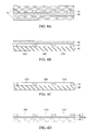
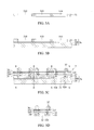
- FIGS. 3A to 3F are schematic cross-sectional views showing a method for fabricating a semiconductor package according to a first embodiment of the present invention, wherein FIGS. 3 C′, 3 E′ and 3 F′ show another embodiment of FIGS. 3C to 3F , and FIGS. 3 D′ and 3 D′′ are schematic upper views showing different embodiments of FIG. 3D (omitting the circuit layer);
- FIGS. 4A to 4F are schematic cross-sectional views showing a method for fabricating a semiconductor package according to a second embodiment of the present invention.
- FIGS. 5A to 5D are schematic cross-sectional views showing a method for fabricating a semiconductor package according to a third embodiment of the present invention.
- FIGS. 6A to 6E are schematic cross-sectional views showing a method for fabricating a semiconductor package according to a fourth embodiment of the present invention, wherein FIGS. 6 A′ and 6 E′ show other embodiments of FIGS. 6A and 6E , respectively.
- FIGS. 3A to 3F are schematic cross-sectional views showing a method for fabricating a semiconductor package 3 according to a first embodiment of the present invention. The method of the present embodiment is performed on a wafer or full panel level.
- a carrier 30 is disposed in a mold 9 . Then, a dielectric material is filled in the mold 9 to form a frame 31 of the dielectric material. Then, the mold 9 is removed. As such, a frame 31 having a plurality of openings 310 is formed on the carrier 30 . The frame 31 having the openings 310 and the carrier 30 constitute a carrier structure 3 a.
- the carrier 30 is made of an inorganic material such as a semiconductor material or ceramic, or a flexible organic material.
- the carrier 30 of an inorganic material is, for example, a silicon-containing substrate such as a glass board.
- the organic material is, for example, polyimide (PI), polybenzoxazole (PBO), benzocyclobutene (BCB) and so on.
- the dielectric material of the frame 21 is made of Si, SiO 2 , Si x N y and so on.
- the mold 9 has a first mold body 9 a and a second mold body 9 b.
- a frame pattern 91 is formed in the first mold body 9 a, and the carrier 30 is disposed on the second mold body 9 b.
- a plurality of semiconductor elements 32 are disposed in the openings 310 of the frame 31 , respectively.
- Each of the electronic elements 32 can be an active element such as a semiconductor chip, a passive element such as a resistor, a capacitor or an inductor, or a combination thereof.
- each of the electronic elements 32 is an active element, which has an active surface 32 a with a plurality of electrode pads 320 and an inactive surface 32 b opposite to the active surface 32 a.
- the electronic elements 32 are disposed in the openings 310 via the inactive surfaces 32 b thereof.
- the electronic elements 32 can be disposed in the openings 310 through a bonding layer (not shown).
- the bonding layer is a die attach film.
- the bonding layer can be formed on the inactive surfaces 32 b of the electronic elements 32 first and then the electronic elements 32 are disposed in the openings 310 through the bonding layer.
- the bonding layer can be formed in the openings 310 by such as dispensing and then the electronic elements 32 are disposed in the openings 310 through the bonding layer.
- the electronic elements 32 are disposed in the openings 310 via the active surfaces 32 a thereof.
- an encapsulant 33 is formed in the openings 310 and on the frame 31 for encapsulating and fixing the electronic elements 32 .
- a circuit layer 34 is formed on the encapsulant 33 , and a plurality of conductive vias 340 are formed in the encapsulant 33 for electrically connecting the circuit layer 34 and the electrode pads 320 of the electronic elements 32 .
- the encapsulant 33 encapsulates the peripheral sides and the active surfaces 32 a of the electronic elements 32 .
- the encapsulant 33 can be made of an inorganic material such as SiO 2 or Si x N y , or an organic material such as polyimide (PI), polybenzoxazole (PBO) or benzocyclobutene (BCB).
- PI polyimide
- PBO polybenzoxazole
- BCB benzocyclobutene
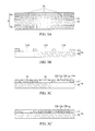
- the carrier 30 can have a rectangular shape, as shown in FIG. 3 D′, or have a circular shape, as shown in FIG. 3 D′′.
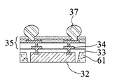
- an RDL process is performed. As such, an RDL structure 35 is formed on the encapsulant 33 and the circuit layer 34 and electrically connected to the circuit layer 34 .
- the RDL structure 35 has a dielectric layer 350 , a circuit layer 351 formed on the dielectric layer 350 , and an insulating layer 36 such as a solder mask layer or a dielectric layer formed on the dielectric layer 350 and the circuit layer 351 .
- the circuit layer 351 is electrically connected to the circuit layer 34 .
- a plurality of openings 360 are formed in the insulating layer 36 for exposing portions of the circuit layer 351 .
- a plurality of conductive elements 37 such as solder balls can be mounted on the exposed portions of the circuit layer 351 .
- the dielectric layer 350 can be made of the same material as the encapsulant 33 .
- the carrier 30 is removed to expose the inactive surfaces 32 b of the electronic elements 32 and a singulation process is performed along a cutting path S of FIG. 3E . As such, a plurality of semiconductor packages 3 are obtained. It should be noted that the frame 31 is left in the packages 3 to support the overall structure and increase the rigidity of the overall structure.
- the carrier 30 is removed to expose the active surfaces 32 a of the electronic elements 32 and then a circuit layer 34 and an RDL structure 35 are formed, as shown in FIG. 3 E′. Thereafter, a singulation process is performed, as shown in FIG. 3 F′.
- the frame 31 and the carrier 30 are separately fabricated.
- the openings 310 of the frame 31 are formed through the mold 9 . Therefore, as long as the frame pattern 91 meets the requirement, the size of the openings 310 can be accurately controlled so as not to form chamfers between the openings 310 and the carrier 30 . On the other hand, even if a chamfer is formed at the bottom of the openings 310 , the accuracy of the chamfer can be effectively controlled.
- FIGS. 4A to 4F are schematic cross-sectional views showing a method for fabricating a semiconductor package 4 according to a second embodiment of the present invention.
- the present embodiment differs from the first embodiment in the process of forming the frame.
- a dielectric material is filled in a mold 9 by molding so as to cause the dielectric material to form a frame 41 and a base portion 40 supporting the frame 41 .
- the dielectric material of the frame 41 and the base portion 40 is a molding compound.
- the molding process can refer to the steps of FIGS. 6 A′ and 6 B (to be described later).
- the mold 9 is removed.
- the frame 41 is formed with a plurality of openings 410 .
- the frame 41 and the base portion 40 are disposed on a support member 42 , with the openings 410 facing the support member 42 .
- the base portion 40 is removed by grinding or sandblasting.
- the support member 42 is removed and then the frame 41 is bonded to a carrier 30 .
- the frame 41 having the openings 410 and the carrier 30 constitute a carrier structure 4 a.
- a bonding layer 300 is formed on the carrier 30 first and then the frame 41 is bonded to the bonding layer 300 .
- the bonding layer 300 can be a die attachment film.
- the bonding layer 300 can be formed by adhesive coating or chemical vapor deposition (CVD).
- the bonding layer 300 can be made of SiO 2 formed by thermal oxidation of a wafer fusion process.
- FIGS. 4E and 4F processes similar to those of FIGS. 3C to 3F (or FIGS. 3 C′, 3 E′ and 3 F′) are performed.
- a plurality of electronic elements 32 are disposed in the openings 410 on the bonding layer 300 , respectively.
- the frame 41 and the carrier 30 are separately fabricated.
- the openings 410 of the frame 41 are formed through the mold 9 . Therefore, as long as the mold 9 meets the requirement, the size of the openings 410 can be accurately controlled so as not to form chamfers between the openings 410 and the carrier 30 . On the other hand, even if a chamfer is formed at the bottom of the openings 410 , the accuracy of the chamfer can be effectively controlled.
- FIGS. 5A to 5D are schematic cross-sectional views showing a method for fabricating a semiconductor package 5 according to a third embodiment of the present invention.
- the present embodiment differs from the first embodiment in the process of forming the frame.
- a semiconductor board is etched to form a frame 51 having a plurality of openings 510 .
- a bonding layer 300 is formed on a carrier 30 and the frame 51 is bonded to the bonding layer 300 of the carrier 31 .
- the frame 51 having the openings 510 , the bonding layer 300 and the carrier 30 constitute a carrier structure 5 a.
- FIGS. 5C and 5D processes similar to those of FIGS. 3C to 3F (or FIGS. 3 C′, 3 E′ and 3 F′) are performed.
- the frame 51 and the carrier 30 are separately fabricated. Therefore, the size of the openings 510 is first determined to meet the requirement and then the frame 51 is disposed on the carrier 30 so as not to form chamfers between the openings 510 and the carrier 30 . On the other hand, even if a chamfer is formed at the bottom of the openings 510 , the accuracy of the chamfer can be effectively controlled.
- FIGS. 6A to 6E are schematic cross-sectional views showing a method for fabricating a semiconductor package 6 according to a fourth embodiment of the present invention.
- the present embodiment differs from the first embodiment in the process of forming the carrier and the frame.
- a mold 9 having a plurality of protruding portions 90 therein is provided.
- the mold 9 has a first mold body 9 a and a second mold body 9 b.
- the protruding portions 90 are formed on the first mold body 9 a.
- a dielectric material is filled in the mold 9 by molding so as to cause the dielectric material to form a carrier 60 and a frame 61 .
- the carrier 60 and the frame 61 are integrally formed and a plurality of openings 610 are formed corresponding in position to the protruding portions 90 of the mold 9 .
- the frame 61 having the openings 610 and the carrier 60 constitute a carrier structure 6 a.
- a dielectric material 8 is formed on the second mold body 9 b first and then the first mold body 9 a and the second mold body 9 b are pressed together so as to cause the dielectric material 8 to form the carrier 60 and the frame 61 .
- the openings 610 are formed corresponding in position to the protruding portions 90 .
- the mold 9 is removed and the carrier structure 6 a consisting of the frame 61 and the carrier 60 is provided.
- the openings 610 have sloped sidewalls relative to the carrier 60 . That is, the sidewalls of the openings 610 are sloped relative to the bottom surfaces of the openings 610 .
- FIGS. 6D and 6E processes similar to those of FIGS. 3C to 3F (or FIGS. 3 C′, 3 E′ and 3 F′) are performed.
- the carrier 60 and the frame 61 are integrally formed.
- the openings 610 are formed through the mold 9 . Therefore, as long as the protruding portions 90 are determined to meet the requirement, the size of the openings 610 can be accurately controlled so as not to form chamfers between the openings 610 and the carrier 60 . On the other hand, even if a chamfer is formed at the bottom of the openings 610 , the accuracy of the chamfer can be effectively controlled.
- the conductive vias can be dispensed with, as shown in FIG. 6 E′.
- the present invention further provides a semiconductor package 3 , 4 , which has: a carrier 30 ; a frame 31 , 41 having a plurality of openings 310 , 410 , wherein the frame 31 , 41 is bonded to the carrier 30 ; a plurality of electronic elements 32 disposed in the openings 310 , 410 of the frame 31 , 41 , respectively; an encapsulant 33 formed in the openings 310 . 410 of the frame 31 , 41 for encapsulating the electronic elements 32 ; and a circuit layer 34 formed on and electrically connected to the electronic elements 32 .
- the carrier 30 can be made of an inorganic material or an organic material.
- the frame 31 , 41 can be made of a material different from that of the carrier 30 .
- the frame 31 , 41 is made of a dielectric material.
- the frame 41 is bonded to the carrier 30 through a bonding layer 300 .
- the present invention further provides a semiconductor package 5 , which has: a carrier 30 ; a frame 51 having a plurality of openings 510 , wherein the frame 51 is bonded to the carrier 30 through a bonding layer 300 ; a plurality of electronic elements 32 disposed in the openings 510 of the frame 51 , respectively; an encapsulant 33 formed in the openings 510 of the frame 51 for encapsulating the electronic elements 32 ; and a circuit layer 34 formed on and electrically connected to the electronic elements 32 .
- the carrier 30 can be made of an inorganic material or an organic material.
- the frame 51 can be made of the same material as the carrier 30 .
- the present invention further provides a semiconductor package 6 , which has: a carrier 60 made of a dielectric material; a frame 61 having a plurality of openings 610 , wherein the frame is bonded to and integrally formed with the carrier 60 ; a plurality of electronic elements 32 disposed in the openings 610 of the frame 60 , respectively; an encapsulant 33 formed in the openings 610 of the frame 60 for encapsulating the electronic elements 32 ; and a circuit layer 34 formed on and electrically connected to the electronic elements 32 .
- the semiconductor package 3 , 4 , 5 , 6 further has an RDL structure 35 formed on the electronic elements 32 and the circuit layer 34 and electrically connected to the circuit layer 34 .
- the present invention further provides a carrier structure 3 a, 4 a, which has: a carrier 30 ; and a frame 31 , 41 having a plurality of openings 310 , 410 , wherein the frame 31 , 41 is bonded to the carrier 30 and made of a material different from that of the carrier 30 .
- the frame 41 is bonded to the carrier 30 through a bonding layer 300 .
- the present invention further provides a carrier structure 5 a, which has: a carrier 30 ; and a frame 51 having a plurality of openings 510 , wherein the frame 51 is bonded to the carrier 30 through a bonding layer 300 and made of the same material as the carrier 30 .
- the carrier 30 can be made of an inorganic material or an organic material.
- the present invention further provides a carrier structure 6 a, which has: a carrier 60 made of a dielectric material; and a frame 61 having a plurality of openings 610 , wherein the frame 61 is bonded to and integrally formed with the carrier 60 .
- the openings 610 have sloped sidewalls relative to the carrier 60 .
- the carrier 30 , 60 can have a rectangular shape or a circular shape.
- no chamfer is formed between the openings 310 , 410 , 510 , 610 and the carrier 30 , 60 .
- the present invention increases the accuracy of positioning of the electronic elements and improves the surface integrity of the semiconductor package, thereby improving the product yield in subsequent processes.
Applications Claiming Priority (2)
| Application Number | Priority Date | Filing Date | Title |
|---|---|---|---|
| TW103131713 | 2014-09-15 | ||
| TW103131713A TWI560827B (en) | 2014-09-15 | 2014-09-15 | Semiconductor package and its carrier structure and method of manufacture |
Publications (1)
| Publication Number | Publication Date |
|---|---|
| US20160079110A1 true US20160079110A1 (en) | 2016-03-17 |
Family
ID=55455456
Family Applications (1)
| Application Number | Title | Priority Date | Filing Date |
|---|---|---|---|
| US14/849,639 Abandoned US20160079110A1 (en) | 2014-09-15 | 2015-09-10 | Semiconductor package, carrier structure and fabrication method thereof |
Country Status (3)
| Country | Link |
|---|---|
| US (1) | US20160079110A1 (zh) |
| CN (1) | CN105405812A (zh) |
| TW (1) | TWI560827B (zh) |
Cited By (3)
| Publication number | Priority date | Publication date | Assignee | Title |
|---|---|---|---|---|
| US11189576B2 (en) | 2016-08-24 | 2021-11-30 | Advanced Semiconductor Engineering, Inc. | Semiconductor device package and a method of manufacturing the same |
| US11348833B2 (en) * | 2016-03-30 | 2022-05-31 | International Business Machines Corporation | IR assisted fan-out wafer level packaging using silicon handler |
| US11393795B2 (en) * | 2020-02-17 | 2022-07-19 | Samsung Electronics Co., Ltd. | Semiconductor package |
Families Citing this family (3)
| Publication number | Priority date | Publication date | Assignee | Title |
|---|---|---|---|---|
| TWI621224B (zh) * | 2017-07-14 | 2018-04-11 | 欣興電子股份有限公司 | 封裝結構及其製造方法 |
| TWI645523B (zh) * | 2017-07-14 | 2018-12-21 | 矽品精密工業股份有限公司 | 封裝結構及其製法 |
| TWI621223B (zh) * | 2017-08-11 | 2018-04-11 | 矽品精密工業股份有限公司 | 電子封裝件及其製法 |
Citations (10)
| Publication number | Priority date | Publication date | Assignee | Title |
|---|---|---|---|---|
| US20010039072A1 (en) * | 2000-03-30 | 2001-11-08 | Hiroshi Nagasawa | Reactive probe chip, composite substrate and method for fabrication of the same |
| US20040046250A1 (en) * | 2002-08-27 | 2004-03-11 | Chua Swee Kwang | Multichip wafer level packages and computing systems incorporating same |
| US20040256686A1 (en) * | 2003-04-08 | 2004-12-23 | Stmicroelectronics S.R.L. | Method for manufacturing a micro-electro-mechanical device, in particular an optical microswitch, and micro-electro-mechanical device thus obtained |
| US7727859B2 (en) * | 2005-06-30 | 2010-06-01 | Semiconductor Energy Laboratory Co., Ltd | Semiconductor device and manufacturing method thereof |
| US7927922B2 (en) * | 2007-12-20 | 2011-04-19 | Chipmos Technologies Inc | Dice rearrangement package structure using layout process to form a compliant configuration |
| US20120020026A1 (en) * | 2010-07-23 | 2012-01-26 | Tessera Research Llc | Microelectronic elements with post-assembly planarization |
| US20150041987A1 (en) * | 2013-08-07 | 2015-02-12 | Taiwan Semiconductor Manufacturing Company, Ltd. | 3D Packages and Methods for Forming the Same |
| US20150206845A1 (en) * | 2014-01-23 | 2015-07-23 | Taiwan Semiconductor Manufacturing Co., Ltd | Interconnect arrangement with stress-reducing structure and method of fabricating the same |
| US9190318B2 (en) * | 2013-10-22 | 2015-11-17 | Globalfoundries Inc. | Method of forming an integrated crackstop |
| US9704830B1 (en) * | 2016-01-13 | 2017-07-11 | International Business Machines Corporation | Semiconductor structure and method of making |
Family Cites Families (6)
| Publication number | Priority date | Publication date | Assignee | Title |
|---|---|---|---|---|
| US6794273B2 (en) * | 2002-05-24 | 2004-09-21 | Fujitsu Limited | Semiconductor device and manufacturing method thereof |
| TWI245350B (en) * | 2004-03-25 | 2005-12-11 | Siliconware Precision Industries Co Ltd | Wafer level semiconductor package with build-up layer |
| CN101021685A (zh) * | 2006-02-16 | 2007-08-22 | 虹创科技股份有限公司 | 基板结构及薄膜图案层的制造方法 |
| CN101064259A (zh) * | 2006-04-25 | 2007-10-31 | 矽品精密工业股份有限公司 | 半导体封装件及其芯片承载结构与制法 |
| TWI384606B (zh) * | 2008-05-30 | 2013-02-01 | Unimicron Technology Corp | 嵌埋半導體元件之封裝結構及其製法 |
| US8119454B2 (en) * | 2008-12-08 | 2012-02-21 | Stmicroelectronics Asia Pacific Pte Ltd. | Manufacturing fan-out wafer level packaging |
-
2014
- 2014-09-15 TW TW103131713A patent/TWI560827B/zh active
- 2014-11-03 CN CN201410613008.5A patent/CN105405812A/zh active Pending
-
2015
- 2015-09-10 US US14/849,639 patent/US20160079110A1/en not_active Abandoned
Patent Citations (11)
| Publication number | Priority date | Publication date | Assignee | Title |
|---|---|---|---|---|
| US20010039072A1 (en) * | 2000-03-30 | 2001-11-08 | Hiroshi Nagasawa | Reactive probe chip, composite substrate and method for fabrication of the same |
| US20040046250A1 (en) * | 2002-08-27 | 2004-03-11 | Chua Swee Kwang | Multichip wafer level packages and computing systems incorporating same |
| US20040256686A1 (en) * | 2003-04-08 | 2004-12-23 | Stmicroelectronics S.R.L. | Method for manufacturing a micro-electro-mechanical device, in particular an optical microswitch, and micro-electro-mechanical device thus obtained |
| US7727859B2 (en) * | 2005-06-30 | 2010-06-01 | Semiconductor Energy Laboratory Co., Ltd | Semiconductor device and manufacturing method thereof |
| US7927922B2 (en) * | 2007-12-20 | 2011-04-19 | Chipmos Technologies Inc | Dice rearrangement package structure using layout process to form a compliant configuration |
| US20120020026A1 (en) * | 2010-07-23 | 2012-01-26 | Tessera Research Llc | Microelectronic elements with post-assembly planarization |
| US20150041987A1 (en) * | 2013-08-07 | 2015-02-12 | Taiwan Semiconductor Manufacturing Company, Ltd. | 3D Packages and Methods for Forming the Same |
| US9190318B2 (en) * | 2013-10-22 | 2015-11-17 | Globalfoundries Inc. | Method of forming an integrated crackstop |
| US20150206845A1 (en) * | 2014-01-23 | 2015-07-23 | Taiwan Semiconductor Manufacturing Co., Ltd | Interconnect arrangement with stress-reducing structure and method of fabricating the same |
| KR20150088170A (ko) * | 2014-01-23 | 2015-07-31 | 타이완 세미콘덕터 매뉴팩쳐링 컴퍼니 리미티드 | 응력 감소 구조체를 갖는 인터커넥트 배열 및 그 제조 방법 |
| US9704830B1 (en) * | 2016-01-13 | 2017-07-11 | International Business Machines Corporation | Semiconductor structure and method of making |
Cited By (5)
| Publication number | Priority date | Publication date | Assignee | Title |
|---|---|---|---|---|
| US11348833B2 (en) * | 2016-03-30 | 2022-05-31 | International Business Machines Corporation | IR assisted fan-out wafer level packaging using silicon handler |
| US11189576B2 (en) | 2016-08-24 | 2021-11-30 | Advanced Semiconductor Engineering, Inc. | Semiconductor device package and a method of manufacturing the same |
| US11837557B2 (en) | 2016-08-24 | 2023-12-05 | Advanced Semiconductor Engineering, Inc. | Semiconductor device package and a method of manufacturing the same |
| US11393795B2 (en) * | 2020-02-17 | 2022-07-19 | Samsung Electronics Co., Ltd. | Semiconductor package |
| US11881472B2 (en) | 2020-02-17 | 2024-01-23 | Samsung Electronics Co., Ltd. | Semiconductor package |
Also Published As
| Publication number | Publication date |
|---|---|
| TWI560827B (en) | 2016-12-01 |
| TW201611216A (zh) | 2016-03-16 |
| CN105405812A (zh) | 2016-03-16 |
Similar Documents
| Publication | Publication Date | Title |
|---|---|---|
| US20160079110A1 (en) | Semiconductor package, carrier structure and fabrication method thereof | |
| TWI710073B (zh) | 具有天線的半導體封裝及其製造方法 | |
| TWI750247B (zh) | 半導體裝置以及其製造方法 | |
| US9666536B2 (en) | Package structure and fabrication method thereof | |
| US9397081B2 (en) | Fabrication method of semiconductor package having embedded semiconductor elements | |
| US9607974B2 (en) | Package structure and fabrication method thereof | |
| TW202038348A (zh) | 天線整合式封裝結構及其製造方法 | |
| US20150125993A1 (en) | Interposer, manufacturing method thereof, semiconductor package using the same, and method for fabricating the semiconductor package | |
| US20170077047A1 (en) | Electronic package and fabrication method thereof | |
| TWI550783B (zh) | 電子封裝件之製法及電子封裝結構 | |
| CN105428329A (zh) | 具有ubm的封装件和形成方法 | |
| US10224243B2 (en) | Method of fabricating electronic package | |
| CN105374731A (zh) | 封装方法 | |
| TWI677035B (zh) | 半導體封裝及半導體封裝的製程方法 | |
| US10461002B2 (en) | Fabrication method of electronic module | |
| US9041189B2 (en) | Semiconductor package and method of fabricating the same | |
| CN111508904A (zh) | 半导体设备封装及其制造方法 | |
| US20160066427A1 (en) | Package structure and fabrication method thereof | |
| KR101605610B1 (ko) | 반도체 디바이스의 제조 방법 및 이에 따른 반도체 디바이스 | |
| US9673140B2 (en) | Package structure having a laminated release layer and method for fabricating the same | |
| CN107887363B (zh) | 电子封装件及其制法 | |
| US20170309589A1 (en) | Semiconductor device and method for manufacturing the same | |
| TWI691041B (zh) | 電子封裝件及其封裝基板與製法 | |
| US20210175196A1 (en) | Method for fabricating electronic package | |
| TWI556381B (zh) | 半導體封裝件及其製法 |
Legal Events
| Date | Code | Title | Description |
|---|---|---|---|
| AS | Assignment |
Owner name: SILICONWARE PRECISION INDUSTRIES CO., LTD., TAIWAN Free format text: ASSIGNMENT OF ASSIGNORS INTEREST;ASSIGNORS:CHUANG, KUAN-WEI;CHIU, SHIH-KUANG;LIN, CHUN-TANG;AND OTHERS;REEL/FRAME:036527/0909 Effective date: 20140811 |
|
| STCB | Information on status: application discontinuation |
Free format text: ABANDONED -- FAILURE TO RESPOND TO AN OFFICE ACTION |