US20030197777A1 - Beam position adjusting method and device for optical scanning apparatus - Google Patents
Beam position adjusting method and device for optical scanning apparatus Download PDFInfo
- Publication number
- US20030197777A1 US20030197777A1 US10/414,391 US41439103A US2003197777A1 US 20030197777 A1 US20030197777 A1 US 20030197777A1 US 41439103 A US41439103 A US 41439103A US 2003197777 A1 US2003197777 A1 US 2003197777A1
- Authority
- US
- United States
- Prior art keywords
- galvanomirrors
- optical
- light
- scanning apparatus
- beams
- Prior art date
- Legal status (The legal status is an assumption and is not a legal conclusion. Google has not performed a legal analysis and makes no representation as to the accuracy of the status listed.)
- Abandoned
Links
Images


Classifications
-
- G—PHYSICS
- G02—OPTICS
- G02B—OPTICAL ELEMENTS, SYSTEMS OR APPARATUS
- G02B26/00—Optical devices or arrangements for the control of light using movable or deformable optical elements
- G02B26/08—Optical devices or arrangements for the control of light using movable or deformable optical elements for controlling the direction of light
- G02B26/10—Scanning systems
- G02B26/12—Scanning systems using multifaceted mirrors
- G02B26/127—Adaptive control of the scanning light beam, e.g. using the feedback from one or more detectors
-
- B—PERFORMING OPERATIONS; TRANSPORTING
- B41—PRINTING; LINING MACHINES; TYPEWRITERS; STAMPS
- B41J—TYPEWRITERS; SELECTIVE PRINTING MECHANISMS, i.e. MECHANISMS PRINTING OTHERWISE THAN FROM A FORME; CORRECTION OF TYPOGRAPHICAL ERRORS
- B41J2/00—Typewriters or selective printing mechanisms characterised by the printing or marking process for which they are designed
- B41J2/435—Typewriters or selective printing mechanisms characterised by the printing or marking process for which they are designed characterised by selective application of radiation to a printing material or impression-transfer material
- B41J2/47—Typewriters or selective printing mechanisms characterised by the printing or marking process for which they are designed characterised by selective application of radiation to a printing material or impression-transfer material using the combination of scanning and modulation of light
- B41J2/471—Typewriters or selective printing mechanisms characterised by the printing or marking process for which they are designed characterised by selective application of radiation to a printing material or impression-transfer material using the combination of scanning and modulation of light using dot sequential main scanning by means of a light deflector, e.g. a rotating polygonal mirror
Definitions
- the present invention relates to a beam position adjusting method and device for an optical scanning apparatus that uses light beams such as laser beams.
- a multibeam exposure device has been known which can be adapted for an image forming apparatus such as a high-speed digital copying apparatus or a high-speed printing apparatus and which simultaneously uses two or more light beams in order to expose a charged area of a photosensitive drum.
- the multibeam exposure device has two or more semiconductor laser elements that emit respective layer beams, an optical member which sets and adjusts the diameter of each laser beam so as to correspond to a desired resolution and which sets the interval between the laser beams in a sub-scanning direction (orthogonal to an axial direction of a photosensitive drum) to a predetermined value, a polarizing device that polarizes all laser beams so as to travel in a main scanning direction (extending along the axial direction of the photosensitive drum), and an image forming lens system that guides the laser beams polarized by the polarizing device, to the charged area of the photosensitive drum to form an image, and other components.
- galvanomirrors are used in each of which a mirror is mounted in a movable member including an electromagnetic coil so that the angle of a mirror face can be slightly varied by controlling the magnitude of a current flowing through the coil.
- the interval between the laser beams in the sub-scanning direction can be set at 42.3 ⁇ m with a resolution of, for example, 600 dpi by fine-tuning the angles of mirror faces of the galvanomirrors.
- a laser position detecting sensor such as a photodiode are utilized.
- the sensor detects the positions of all laser beams. Then, on the basis of results of the detection, the interval between the lasers is adjusted.
- the interval between the laser beams in the sub-scanning direction can be set at a predetermined value.
- a current with a certain value flows through the electromagnetic coil. The current allows the inclination of the mirror face to be maintained at a predetermined value.
- a beam position adjusting method for adjusting angles of surfaces of galvanomirrors by supplying predetermined power with respect to positions which detect positions on the sensors through which laser beams to be scanned pass so that the passage positions of the light passing through the sensors from driving control means to the galvanomirrors comprising:
- an optical scanning apparatus using galvanomirrors each having a mirror face the angle of which can be changed by supplying power to the galvanomirror, the apparatus also using sensors which
- [0017] detects positions on the sensors through which laser beams to be scanned pass so that the passage positions of the light passing through the sensors can be adjusted by changing the angles of mirror faces of the galvanomirrors, the apparatus comprising:
- a storage section which stores the value of power supplied to the galvanomirrors as information on mirror face angles at which the galvanomirrors are located;
- storage control means for causing the storage section to store the information on the angles of the mirror faces while not supplying power to the galvanomirrors;
- driving control means for reading the information on the angles of the mirror faces stored in the storage section while supplying the power to the galvanomirrors and for displacing the galvanomirrors on the basis of the information on the angles of the mirror faces.
- an optical scanning apparatus comprising:
- optical-path aligning means for positioning light beams from the respective light sources at predetermined intervals in a first direction to synthesize the light beams so that the beams appear single;
- polarizing means for polarizing the light beams form the respective light sources synthesized by the optical-path aligning means so that the beams travel along a second direction orthogonal to the first direction;
- displacement detecting means for detecting displacement of the optical-path aligning means with respect to the first direction by detecting at least one of the light beams from the respective light sources which are polarized by the polarizing means;
- a storage section which stores the displacement of the optical-path aligning means detected by the displacement detecting means
- a driving means for energizing the optical-path aligning means and for aligning the displacement of the optical-path aligning means so as to provide such light beams that the light beams from the respective light sources can be considered to be single.
- FIG. 1 is a schematic view showing a configuration of a digital copying apparatus having a multibeam exposure device to which an embodiment of the present invention is applied;
- FIG. 2 is a schematic view showing a multibeam exposure device incorporated into the digital copying apparatus shown in FIG. 1;
- FIG. 3 is a schematic block diagram illustrating an example of a control system of the multibeam exposure device shown in FIG. 2;
- FIG. 4 is an exploded perspective view illustrating a configuration of galvanomirrors incorporated into the multibeam exposure device shown in FIG. 3;
- FIG. 5 is a block diagram showing a beam position detecting circuit that detects the positions of beams using a beam position detecting sensor in the multibeam exposure shown in FIG. 2;
- FIG. 6 is a schematic view illustrating the characteristics of a detecting surface of the beam position detecting sensor incorporated into the multibeam exposure device shown in FIG. 2;
- FIG. 7 is a flow chart illustrating a step of adjusting the angles of galvanomirrors using the beam position detecting sensor having the detecting surface shown in FIG. 6.
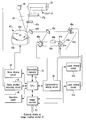
- FIG. 1 schematically shows a configuration of an image forming apparatus (digital copying apparatus) using a multibeam exposure device that simultaneously uses two or more beams.
- the digital copying apparatus 1 has a scanner section 10 and a printer section 20 .
- the scanner section 10 has a first carriage 11 formed so as to be movable in the direction of an arrow in the figure, a second carriage 12 moved so as to follow the first carriage 11 , an optical lens 13 that provides light from the second carriage 12 with predetermined image forming characteristics, a photoelectric converting element 14 such as a CCD sensor which photoelectrically converts the light provided with the predetermined image forming characteristics by the optical lens 13 , to output an electric signal, an original table 16 that holds an original 15 , an original fixing cover 17 that tightly contacts the original 15 with the original table 16 , and other components.
- the first carriage 11 is provided with a light source 18 that illuminates the original 15 and a mirror 11 a that reflects light reflected by the original 15 illuminated by light emitted by the light source 18 , toward the second carriage 12 .
- the second carriage 12 is provided with a mirror 12 a that bends light transmitted by the mirror 11 a of the first carriage 11 , through 90°, and a mirror 12 b that further bends light bent by the mirror 12 a , through 90°.
- Image light incident on the optical lens 13 is collected on a light receiving surface of the photoelectric converting element 14 by the optical lens 13 .
- the image light from the original 15 is sequentially collected on the photoelectric converting element 14 by moving the first carriage 11 and the second carriage 12 along the original table 16 at a relative speed ratio of 2:1.
- the photoelectric converting element 14 converts the image light into a digital signal corresponding to the density of the image.
- the printer section 20 has a multibeam exposure device 21 and an image forming section 22 that forms an image on a recording sheet P by an electrophotographic method.
- the image forming section 22 comprises a drum-shaped photosensitive member having a photosensitive layer formed on its surface, i.e. a photosensitive drum 23 , a charging device 24 that applies a potential of a predetermined polarity to the surface of the photosensitive drum 23 , a developing device 25 that supplies toner to a latent image formed on the surface of the photosensitive drum 23 by the multibeam exposure device 21 , a transfer device 26 that applies an electric field to a toner image formed by development carried out by the developing device 25 , to transfer the toner image to the recording sheet P, a separating device 27 that separates the recording paper P to which the toner image has been transferred, from the photosensitive drum 23 , a cleaning device 28 that removes toner remaining on the surface of the photosensitive drum 23 after the toner image has been transferred to the sheet P, to return the potential distribution of the photosensitive drum 23 to its state prior to charging.
- a charging device 24 that applies a potential of a predetermined polarity to the surface of the photosensitive drum 23
- the charging device 24 , the developing device 25 , the transfer device 26 , the separating device 27 , and the cleaning device 28 are sequentially arranged along the direction of an arrow in which the photosensitive drum 23 is rotated. Further, laser beams from the multibeam exposure device 21 are applied to an exposure position X between the charging device 24 and the developing device 25 .
- An image processing section executes, for example, edge enhancement or a half-tone-processing for half tone images on an image signal read from the original 15 by the scanner section 10 , to convert this signal into a print signal.
- This print signal is then converted into a laser modulating signal used to vary the light intensity of laser beams emitted by a semiconductor laser element in the multibeam exposure device 21 .
- Laser beams from the multibeam exposure device 21 form an electrostatic latent image at the exposure position X in the photosensitive drum 23 .
- the electrostatic latent image formed on the surface of the photosensitive drum 23 is developed using toner from the developing device 25 , and is then carried to a position opposite to the transfer device 26 by rotating the photosensitive member 23 .
- one recording sheet P is taken out of a sheet cassette 29 by a sheet feeding roller 30 and a separating roller 31 .
- the sheet P is then carried to a transfer position at which the transfer device 26 and the photosensitive drum 23 are opposite each other while required timings are being adjusted by an aligning roller 32 .
- the toner image formed on the photosensitive drum 23 is transferred to the recording sheet P at the transfer position by an electric field from the transfer device 26 .
- the recording sheet P to which the toner image has been transferred is separated from the photosensitive drum 23 by the separating device 27 and then guided to a fixing device 34 by a carrying device 33 .
- the fixing device 34 then heats and presses the recording sheet P guided to the fixing device 34 , to fix the electrostatically attached toner.
- the sheet P to which the toner is fixed is discharged to a tray 36 by a sheet discharging roller 35 .
- the photosensitive drum 23 to which the toner image has been transferred by the transfer device 26 continues to be rotated.
- the cleaning device 28 removes toner remaining on the surface of photosensitive drum 23 after the transfer. Furthermore, the cleaning device 28 returns the photosensitive drum 23 to its initial condition set before the potential is supplied to its surface. Then, the next image can be formed.
- Continuous image formation can be accomplished by repeating the above steps.
- FIG. 2 shows the multibeam exposure device 21 from which a housing (body frame) has been removed and some mirrors are omitted and in which optical paths of laser beams are shown on the same plane.
- the multibeam exposure device 21 is provided with semiconductor laser elements 41 a and 41 b as a light beam generating source as shown in FIG. 2.
- the laser beams La and Lb are then guided to a polarizing device 43 having a polygon mirror 43 a . That is, the laser beam La passes through the pre-polarization optical system 42 a , a half mirror 42 c , and a cylinder lens 42 d that converges the light in the sub-scanning direction.
- the laser beam La is guided to the polarizing device 43 having the polygon mirror 43 a .
- the laser beam Lb passes through the pre-polarization optical system 42 b and is then reflected by the half mirror 42 c .
- the laser beam Lb reflected by the half mirror 42 c passes through the cylinder lens 42 d and is then guided to an arbitrary face of the polygon mirror 43 a.
- the cross sections of beam spots of the laser beams La and Lb from the semiconductor laser elements 41 a and 41 b , respectively, are adjusted to predetermined shapes by the pre-polarization optical systems 42 a and 42 b .
- the pre-polarization optical systems 42 a and 42 b comprise finite focus lenses 44 a and 44 b , respectively, that provide predetermined convergent nature to divergent laser beams from the semiconductor laser elements 41 a and 41 b ; diaphragms 45 a and 45 b , respectively, that adjust the cross sections of the laser beams having passed through the finite focus lenses 44 a and 44 b , to predetermined shapes; and galvanomirrors 46 a and 46 b , respectively, which bend the laser beams having passed through the diaphragms 45 a and 45 b and then guide them to the half mirror 42 c and which adjust the positions of the two laser beams La and Lb so as to set the interval between the beams in the sub-scanning direction at a
- the finite focus lenses 44 a and 44 b may be, for example, aspherical glass lenses or single lenses each formed by sticking an ultraviolet-setting plastic aspherical lens to a spherical glass lens.
- the galvanomirrors 46 a and 46 b each include an optical-path changing device that can finely and arbitrarily vary the direction in which the laser beam is reflected.
- the individual mirror faces of the galvanomirrors 46 a and 46 b have their inclinations, i.e. (reflection) angles arbitrarily and independently varied by a galvanomirror driving circuit 58 , described below with reference to FIG. 3.
- the laser beam La from the first laser element 41 a reflected by the galvanomirror 46 a and the laser beam Lb from the second laser element 41 b reflected by the galvanomirror 46 b are integrated into synthesized laser beams (La+Lb) at the parallel direction by the half mirror 42 c .
- the synthesized laser beams appear single as viewed from a planar direction (main scanning direction) as shown in FIG. 2, and have a predetermined interval between themselves in the sub-scanning direction, which is orthogonal to the parallel direction.
- the cylinder lens 42 d further provides the synthesized laser beams (La+Lb) with convergent nature in the sub-scanning direction and then guides them to the polarizing device 43 .
- the polarizing device 43 is a rotating polygon mirror in which a regular polyhedral polygon mirror 43 a is rotated at a predetermined speed by a motor 43 b , the polygon mirror 43 a having eight planar reflection mirrors formed on its outer peripheries.
- a post-polarization optical system 47 including a doublet lens system including a first and second image forming lenses 47 a and 47 b that provide predetermined optical characteristics to synthesized laser beams L (La+Lb) polarized (scanned) by each reflecting surface of the polygon mirror 43 a of the polarizing device 43 to travel in predetermined directions; a beam position detecting sensor 48 that detects that the leaser beams La and Lb of the laser beam L (La+Lb) emitted by the second image forming lens 47 b of the post-polarization optical system 47 have reached predetermined positions located in front of an area in which an image is written (passage timing), the sensor 48 also detecting these predetermined positions; a reflecting mirror 49 arranged between the post-polarization optical system 47 and the beam position detecting sensor 48 to reflect the synthesized
- a CPU (Central Processing Unit) 51 provides such control that data is written to and/or read from a nonvolatile memory 52 or an image memory 53 .
- a motor driving circuit 54 rotates the motor 43 b of the polarizing device 43 at a predetermined speed.
- a beam position detecting circuit 55 detects the positions of laser beams on the basis of a detection signal from the beam position detecting sensor 48 .
- Laser driving circuits 57 a and 57 b cause the semiconductor laser elements 41 a and 41 b to output laser beams of a predetermined wavelength. Further, a galvanomirror driving circuit 58 provided with a D/A converter sets the inclinations of mirror faces of the galvanomirrors 46 a and 46 b . The galvanomirror driving circuit 58 can control driving of individual mirrors 100 according to different instruction values for the galvanomirrors 46 a and 46 b.
- the semiconductor laser elements 41 a and 41 b emit the laser beams La and Lb having their light intensities changed so as to correspond to image data stored in the image memory 53 .
- the laser beam emitted by each of the laser elements 41 a and 41 b has an intensity lower than that sufficient to form a latent image on the photosensitive drum 23 . This is because the magnitude of a laser driving current from each of the laser driving circuits 57 a and 57 b , the magnitude corresponding to control carried out by the CPU 51 , is kept small until the rotation speed of the polygon mirror 43 a reaches a predetermined value.
- the galvanomirrors 46 a and 46 b each have a plate spring 101 that holds the mirror 100 so that its angle can be changed, and a frame 102 that supports the plate spring 101 so as to be movable in an arbitrary direction.
- the plate spring 101 is provided with a bobbin 103 a constituting a thrust generating section 103 that generates force required to move the plate spring 101 , and a coil 103 b housed inside the bobbin 103 a .
- the plate spring 101 is composed of beryllium copper, spring stainless steel SUS 304 , or the like.
- the plate spring 101 is provided with a support surface 101 a that supports the mirror 100 , holding surfaces 101 b utilized to connect to the frame 102 , and a torsion bar portion 101 c as a torsion deformation portion that connects the holding surfaces 101 b and the support surface 101 a together.
- the mirror 100 can be rotated in the direction of an arrow S by twisting the torsion bar 101 c in a predetermined direction.
- the plate spring 101 is fixed, using screws, to threaded holes 102 a formed in the frame 102 , together with spring pressers 104 formed of, for example, resin.
- a magnet 103 c is housed inside the coil 103 b to provide a magnetic field required to generate force that rotationally moves the plate spring 101 if a current flows through the coil 103 b .
- the magnet 103 c is fixed to a central portion of a fixing plate 105 and thus to a predetermined position of the exposure device 21 .
- the frame 102 supports the plate spring 101 that holds the mirror 100 , and is mounted integrally with the fixing plate 105 .
- the bobbin 103 a in which the magnet 103 c and the coil 103 b are housed is spaced from the frame 102 by a predetermined distance.
- a damping material such as silicone gel is filled into the gap between the frame 102 and the bobbin 103 a to prevent the mirror 100 from being vibrated by disturbance vibration or the like.
- the frame 102 functions as a yoke constituting a magnetic circuit for a magnetic line of force from the magnet 103 c.
- the galvanomirror driving circuit 58 supplies a current of a predetermined polarity to the coils 103 b of the galvanomirrors 46 a and 46 b .
- Magnetic force generated between the coil 103 b and the magnet 103 c twists the support surface 101 a of the plate spring 101 to rotationally move the mirror 100 in the direction of the arrow S according to an instruction value.
- the rotational movement of the mirror 100 adjusts the directions of laser beams reflected by a mirror face, i.e. their positions in the sub-scanning direction.
- the angle at which the mirror 100 is located is maintained by retaining the magnitude of a current supplied to the coil 103 b.
- the angle through which the mirror 100 is rotationally moved is determined by an instruction value from the CPU 51 .
- An 8-bit instruction value can vary the angle of the mirror 100 through 256 levels.
- the beam position detecting sensor 48 has a square light receiving surface composed of a sensor 48 A and a sensor 48 B. As shown in FIG. 6, the sensor 48 A and 48 b respectively has a light receiving surface (detecting areas) and each is a right-angled triangle. The detecting area of the sensor 48 B has a lateral-side (longer side) being arranged parallel with a lateral-side of the detecting area of the sensor 48 A. The sensors 48 A and 48 B are formed to have substantially the same area. Accordingly, the sensors 48 A and 48 B output a current of the same magnitude when light of the same intensity passes through their centers. Further, before shipment, a correction amount for output from one of the sensors is set and stored in an NVRAM.
- the sensor 48 A receives this laser beam for a longer time, while the sensor 48 B receives it for a shorter time. This enables the detection of the position on the light receiving surface through which the laser beam has passed.
- a beam position detecting circuit 55 has a current/voltage converting circuit 61 that converts an output from the sensor 48 A into a voltage signal, and a current/voltage converting circuit 62 that converts an output from the sensor 48 B into a voltage signal.
- the voltage signals from the current/voltage converting circuits 61 and 62 are amplified by a differential amplifier 63 .
- the differential amplifier 63 then outputs the difference between these voltage signals.
- the output from the differential amplifier 63 is integrated by an integrating circuit 64 .
- An output from the integrating circuit 64 is compared with a set value by a wind comparator 65 and then outputted to a driver 65 .
- An output from the beam position detecting circuit 55 is binarized by the driver 66 and then supplied to the CPU 51 as sub-scanning position detection data.
- the current/voltage converting circuits 61 and 62 , the differential amplifier 63 , the integrating circuit 64 , and the wind comparator 65 are each composed of an ASIC.
- the plate spring 101 holding the mirror 100 is fixed at a position where it is balanced owing to its own weight. This is because no current is supplied to the coil 103 of the galvanomirror 46 a or 46 b .
- the polygon mirror 43 a is rotated to cause the semiconductor laser elements 41 a and 41 b to emit the laser beams La and Lb, respectively, the beams La and Lb are reflected by the mirrors 100 of the galvanomirrors 46 a and 46 b , respectively.
- the laser beams La and Lb are collected on that part of surface of the photosensitive drum 23 which is off a predetermined position in the sub-scanning direction.
- the sensors 48 A and 48 B of the position detecting sensor 48 detect the positions on themselves through which the laser beams La and Lb have passed.
- the sensors 48 A and 48 B of the beam position detecting sensor 48 it is impossible for the sensors 48 A and 48 B of the beam position detecting sensor 48 to detect the positions of the lasers La and Lb if these beams do not pass through the sensors. Much labor and time is required to make such adjustment that the laser beams La and Lb can pass through the sensors 48 A and 48 B. Even if the laser beams La and Lb pass through the sensors 48 A and 48 B of the beam position detecting sensor 48 , when the position on the sensor 48 A through which the laser beam passes markedly deviates from the position on the sensor 48 B through which the laser beam passes, much labor and time is required to make such adjustment that the laser beams La and Lb pass through a predetermined position.
- the CPU 51 reads the galvano instruction values stored in the nonvolatile memory 52 as positional information on the laser beams La and Lb passing through the sensors 48 A and 48 B of the beam position detecting sensor 48 last time the power is turned off. The CPU 51 then controls the galvanomirror driving circuit 58 on the basis of these galvano instruction values.
- the CPU 51 determines that the semiconductor laser elements 41 a and 41 b will emit the laser beams La and Lb, respectively. Then, at step S 1 , the CPU reads the galvano instruction values (positional information on the laser beams La and Lb passing through the sensors 48 A and 48 B of the beam position detecting sensor 48 last when the predetermined current is cut off (i.e. when the power to each section is turned off), the current being supplied to each section, not described in detail, before the multibeam exposure device 21 carries out exposure).
- the read galvano instruction values are provided to the galvanomirror driving circuit 58 .
- the coils 103 b of the galvanomirrors 46 a and 46 b are supplied with respective predetermined currents (driving control means).
- step S 2 the semiconductor laser elements 41 a and 41 b are driven to emit the beams La and Lb.
- the galvanomirrors 46 a and 46 b can adjust the directions in which the laser beams La and Lb from the semiconductor laser elements 41 a and 41 b , respectively, are reflected.
- the predetermined current is cut off (i.e. when the power to each section is turned off), the current being supplied to each section, not described in detail, before the multibeam exposure device 21 carries out exposure.
- the CPU 51 stores the last galvano instruction values supplied to the galvanomirror driving circuit 58 , in the nonvolatile memory 52 to end processing (storage control means).
- the CPU 51 can read the last galvano instruction values (supplied last during step S 2 ) from the nonvolatile memory 52 and adjust the galvano mirror driving circuit 58 on the basis of these galvano instruction values.
- the predetermined current is supplied only to the semiconductor laser element 41 a , with the laser beam La directly reflected by the polygon mirror 43 a .
- the laser beam La reflected by the galvanomirror 46 a is reflected by the polygon mirror 43 a .
- the post-polarization optical system 47 expose the photosensitive drum 23 to the laser beam La.
- the laser beam La from the polygon mirror 43 a is incident on the reflected beam position detecting sensor 48 .
- the mirror 100 of the galvanomirror 46 a is located at a predetermined angle according to the last galvano instruction values.
- the laser beam La from the semiconductor laser element 41 a can reliably pass through the sensors 48 A and 48 B of the beam position detecting sensor 48 . Further, the positions on the sensors 48 A and 48 B through which the laser beam La passes do-not deviate from the desired ones.
- fine-tuning the galvanomirror 46 a serves to reduce the time required to adjust the laser beam La to the desired position.
- the predetermined current is supplied only to the semiconductor laser element 41 b .
- the laser beam Lb is directly reflected by the polygon mirror 43 a .
- the post-polarization optical system 47 expose the photosensitive drum 23 to the laser beam Lb. Further, the laser beam Lb from the polygon mirror 43 a is incident on the beam position detecting sensor 48 .
- the mirror 100 of the galvanomirror 46 b is located at a predetermined angle according to the last galvano instruction values.
- the laser beam Lb from the semiconductor laser element 41 b can reliably pass through the sensors 48 A and 48 B of the beam position detecting sensor 48 . Further, the positions on the sensors 48 A and 48 B through which the laser beam Lb passes do not deviate from the desired ones.
- fine-tuning the galvanomirror 46 b serves to reduce the time required to adjust the laser beam Lb to the desired position.
- the laser beams La and Lb are simultaneously emitted by the semiconductor laser elements 41 a and 41 b , respectively.
- the laser beams La and Lb are simultaneously collected at the exposure position X on the photosensitive drum 23 .
- the interval in the sub-scanning direction is 42.3 ⁇ m with a resolution of 600 dpi.
- the laser beams are used as light beams.
- the exposure device of the present invention is not limited to this aspect.
- the multibeam exposure device is used. It should be appreciated that the optical scanning device of the present invention is not limited to the multibeam exposure device.
- the present invention can provide a beam position adjusting method and device for an optical scanning apparatus which enables, even when reset during standby, the angles of mirror faces of the galvanomirrors to be easily adjusted to reduce the time required to adjust the positions of light beams.
Landscapes
- Physics & Mathematics (AREA)
- General Physics & Mathematics (AREA)
- Optics & Photonics (AREA)
- Facsimile Scanning Arrangements (AREA)
- Mechanical Optical Scanning Systems (AREA)
- Facsimile Heads (AREA)
- Laser Beam Printer (AREA)
- Mechanical Light Control Or Optical Switches (AREA)
Priority Applications (1)
| Application Number | Priority Date | Filing Date | Title |
|---|---|---|---|
| US11/054,426 US20050146595A1 (en) | 2002-04-18 | 2005-02-10 | Beam position adjusting method and device for optical scanning apparatus |
Applications Claiming Priority (2)
| Application Number | Priority Date | Filing Date | Title |
|---|---|---|---|
| JP2002116211A JP2003307690A (ja) | 2002-04-18 | 2002-04-18 | 光走査装置のビーム位置調整方法及びビーム位置調整装置 |
| JP2002-116211 | 2002-04-18 |
Related Child Applications (1)
| Application Number | Title | Priority Date | Filing Date |
|---|---|---|---|
| US11/054,426 Continuation US20050146595A1 (en) | 2002-04-18 | 2005-02-10 | Beam position adjusting method and device for optical scanning apparatus |
Publications (1)
| Publication Number | Publication Date |
|---|---|
| US20030197777A1 true US20030197777A1 (en) | 2003-10-23 |
Family
ID=29207741
Family Applications (2)
| Application Number | Title | Priority Date | Filing Date |
|---|---|---|---|
| US10/414,391 Abandoned US20030197777A1 (en) | 2002-04-18 | 2003-04-16 | Beam position adjusting method and device for optical scanning apparatus |
| US11/054,426 Abandoned US20050146595A1 (en) | 2002-04-18 | 2005-02-10 | Beam position adjusting method and device for optical scanning apparatus |
Family Applications After (1)
| Application Number | Title | Priority Date | Filing Date |
|---|---|---|---|
| US11/054,426 Abandoned US20050146595A1 (en) | 2002-04-18 | 2005-02-10 | Beam position adjusting method and device for optical scanning apparatus |
Country Status (2)
| Country | Link |
|---|---|
| US (2) | US20030197777A1 (ja) |
| JP (1) | JP2003307690A (ja) |
Cited By (2)
| Publication number | Priority date | Publication date | Assignee | Title |
|---|---|---|---|---|
| US20050128546A1 (en) * | 2003-12-15 | 2005-06-16 | Canon Kabushiki Kaisha | Optical deflector |
| US20120242872A1 (en) * | 2009-11-17 | 2012-09-27 | Canon Kabushiki Kaisha | Optical-image pickup apparatus and method for controlling the same |
Families Citing this family (2)
| Publication number | Priority date | Publication date | Assignee | Title |
|---|---|---|---|---|
| US20060197821A1 (en) * | 2005-03-07 | 2006-09-07 | Yung-Shan Lin | Apparatus for image correction of a laser printer and method for the same |
| US7826070B2 (en) * | 2007-08-17 | 2010-11-02 | Kabushiki Kaisha Toshiba | Scanning optical system adjusting device and scanning optical system adjusting method |
Citations (4)
| Publication number | Priority date | Publication date | Assignee | Title |
|---|---|---|---|---|
| US5539719A (en) * | 1994-02-17 | 1996-07-23 | Konica Corporation | Light beam deviation detecting device used in an image forming apparatus |
| US6188424B1 (en) * | 1998-01-22 | 2001-02-13 | Toshiba Tec Corporation | Light beam scanning, image forming apparatus, and method of adjusting the image forming apparatus |
| US6323889B1 (en) * | 1998-11-13 | 2001-11-27 | Toshiba Tec Kabushiki Kaisha | Multi-beam exposure apparatus having mirror tilt angle control, image forming apparatus that employs the exposure apparatus, and image forming method |
| US6496213B1 (en) * | 1999-09-28 | 2002-12-17 | Toshiba Tec Kabushiki Kaisha | Multi-beam control method |
Family Cites Families (2)
| Publication number | Priority date | Publication date | Assignee | Title |
|---|---|---|---|---|
| JP4308338B2 (ja) * | 1998-01-16 | 2009-08-05 | 株式会社東芝 | ビーム光走査装置および画像形成装置 |
| JP4567829B2 (ja) * | 1999-09-24 | 2010-10-20 | 東芝テック株式会社 | ビーム光走査装置 |
-
2002
- 2002-04-18 JP JP2002116211A patent/JP2003307690A/ja not_active Abandoned
-
2003
- 2003-04-16 US US10/414,391 patent/US20030197777A1/en not_active Abandoned
-
2005
- 2005-02-10 US US11/054,426 patent/US20050146595A1/en not_active Abandoned
Patent Citations (4)
| Publication number | Priority date | Publication date | Assignee | Title |
|---|---|---|---|---|
| US5539719A (en) * | 1994-02-17 | 1996-07-23 | Konica Corporation | Light beam deviation detecting device used in an image forming apparatus |
| US6188424B1 (en) * | 1998-01-22 | 2001-02-13 | Toshiba Tec Corporation | Light beam scanning, image forming apparatus, and method of adjusting the image forming apparatus |
| US6323889B1 (en) * | 1998-11-13 | 2001-11-27 | Toshiba Tec Kabushiki Kaisha | Multi-beam exposure apparatus having mirror tilt angle control, image forming apparatus that employs the exposure apparatus, and image forming method |
| US6496213B1 (en) * | 1999-09-28 | 2002-12-17 | Toshiba Tec Kabushiki Kaisha | Multi-beam control method |
Cited By (6)
| Publication number | Priority date | Publication date | Assignee | Title |
|---|---|---|---|---|
| US20050128546A1 (en) * | 2003-12-15 | 2005-06-16 | Canon Kabushiki Kaisha | Optical deflector |
| US7149017B2 (en) * | 2003-12-15 | 2006-12-12 | Canon Kabushiki Kaisha | Optical deflector |
| US20070103752A1 (en) * | 2003-12-15 | 2007-05-10 | Canon Kabushiki Kaisha | Optical deflector |
| US7242506B2 (en) | 2003-12-15 | 2007-07-10 | Canon Kabushiki Kaisha | Optical deflector |
| US20120242872A1 (en) * | 2009-11-17 | 2012-09-27 | Canon Kabushiki Kaisha | Optical-image pickup apparatus and method for controlling the same |
| US9107619B2 (en) * | 2009-11-17 | 2015-08-18 | Canon Kabushiki Kaisha | Optical-image pickup apparatus and method for controlling the same |
Also Published As
| Publication number | Publication date |
|---|---|
| JP2003307690A (ja) | 2003-10-31 |
| US20050146595A1 (en) | 2005-07-07 |
Similar Documents
| Publication | Publication Date | Title |
|---|---|---|
| CN101261365B (zh) | 光学扫描装置和图像形成设备 | |
| KR100477495B1 (ko) | 광-주사 광학 시스템 및 이를 포함한 이미지-형성 장치 | |
| US6323889B1 (en) | Multi-beam exposure apparatus having mirror tilt angle control, image forming apparatus that employs the exposure apparatus, and image forming method | |
| US7218337B2 (en) | Optical scanner, optical-path adjustment method, and image forming apparatus | |
| US20050146595A1 (en) | Beam position adjusting method and device for optical scanning apparatus | |
| JP2004184657A (ja) | 走査光学装置及びそれを用いた画像形成装置 | |
| US5821971A (en) | Image registration for a raster output scanner (ROS) color printer | |
| JP4077235B2 (ja) | 光走査装置のビーム位置調整方法 | |
| US6958471B2 (en) | Method and apparatus for forming image | |
| EP1094351A2 (en) | Multi-beam scanning optical apparatus and image forming apparatus using it | |
| JPH03245116A (ja) | 光学装置及びこの光学装置が組込まれる画像形成装置或いは画像情報読取装置 | |
| US8976423B2 (en) | Optical scanning system and imaging apparatus for using same | |
| US6888561B2 (en) | Beam control device | |
| JP4669656B2 (ja) | 電子写真装置 | |
| JP2000147399A (ja) | 露光装置およびこの露光装置を含む画像形成装置 | |
| JP4060423B2 (ja) | 画像形成装置 | |
| JP2988682B2 (ja) | 光学装置及びこの光学装置が組込まれる画像形成装置或いは画像読取装置 | |
| JP2550608Y2 (ja) | 走査光学系 | |
| JP2001343603A (ja) | マルチビーム光源走査装置 | |
| JPH11212008A (ja) | 光走査装置、画像形成装置及び光走査装置の光軸調整装置 | |
| JPH10149427A (ja) | 光学走査装置及び光学情報読取装置並びに光学情報記録装置 | |
| JPH0698105A (ja) | 画像読み取り・記録装置 | |
| US7256812B2 (en) | Laser exposing apparatus | |
| JPH04264512A (ja) | 光学装置及びこの光学装置が組込まれる画像形成装置 | |
| JPH11227251A (ja) | マルチビーム露光装置 |
Legal Events
| Date | Code | Title | Description |
|---|---|---|---|
| AS | Assignment |
Owner name: KABUSHIKI KAISHA TOSHIBA, JAPAN Free format text: ASSIGNMENT OF ASSIGNORS INTEREST;ASSIGNOR:MIURA, TATSUYUKI;REEL/FRAME:013970/0744 Effective date: 20030409 Owner name: TOSHIBA TEC KABUSHIKI KAISHA, JAPAN Free format text: ASSIGNMENT OF ASSIGNORS INTEREST;ASSIGNOR:MIURA, TATSUYUKI;REEL/FRAME:013970/0744 Effective date: 20030409 |
|
| STCB | Information on status: application discontinuation |
Free format text: ABANDONED -- FAILURE TO RESPOND TO AN OFFICE ACTION |