US20020041214A1 - PLL circuit - Google Patents
PLL circuit Download PDFInfo
- Publication number
- US20020041214A1 US20020041214A1 US09/964,743 US96474301A US2002041214A1 US 20020041214 A1 US20020041214 A1 US 20020041214A1 US 96474301 A US96474301 A US 96474301A US 2002041214 A1 US2002041214 A1 US 2002041214A1
- Authority
- US
- United States
- Prior art keywords
- signal
- inputted
- nand
- circuit
- circuits
- Prior art date
- Legal status (The legal status is an assumption and is not a legal conclusion. Google has not performed a legal analysis and makes no representation as to the accuracy of the status listed.)
- Abandoned
Links
- 230000003068 static effect Effects 0.000 claims description 70
- 230000010355 oscillation Effects 0.000 claims description 41
- 239000003990 capacitor Substances 0.000 claims description 40
- 239000013256 coordination polymer Substances 0.000 claims 22
- 101000851007 Homo sapiens Vascular endothelial growth factor receptor 2 Proteins 0.000 description 18
- 102100033177 Vascular endothelial growth factor receptor 2 Human genes 0.000 description 18
- 238000010586 diagram Methods 0.000 description 10
- 238000013016 damping Methods 0.000 description 9
- 238000000034 method Methods 0.000 description 6
- 230000002349 favourable effect Effects 0.000 description 5
- 230000008569 process Effects 0.000 description 5
- 101150110971 CIN7 gene Proteins 0.000 description 4
- 101000932478 Homo sapiens Receptor-type tyrosine-protein kinase FLT3 Proteins 0.000 description 4
- 101150110298 INV1 gene Proteins 0.000 description 4
- 102100020718 Receptor-type tyrosine-protein kinase FLT3 Human genes 0.000 description 4
- 101100397044 Xenopus laevis invs-a gene Proteins 0.000 description 4
- 244000145845 chattering Species 0.000 description 4
- 230000000630 rising effect Effects 0.000 description 4
- 230000001360 synchronised effect Effects 0.000 description 4
- 230000009466 transformation Effects 0.000 description 4
- 230000000694 effects Effects 0.000 description 3
- 238000005516 engineering process Methods 0.000 description 3
- 239000010453 quartz Substances 0.000 description 3
- 230000009467 reduction Effects 0.000 description 3
- VYPSYNLAJGMNEJ-UHFFFAOYSA-N silicon dioxide Inorganic materials O=[Si]=O VYPSYNLAJGMNEJ-UHFFFAOYSA-N 0.000 description 3
- 230000007704 transition Effects 0.000 description 3
- 239000000470 constituent Substances 0.000 description 2
- 230000006872 improvement Effects 0.000 description 2
- 238000010295 mobile communication Methods 0.000 description 2
- 230000004044 response Effects 0.000 description 2
- 230000001052 transient effect Effects 0.000 description 2
- 230000006399 behavior Effects 0.000 description 1
- 230000001413 cellular effect Effects 0.000 description 1
- 230000008859 change Effects 0.000 description 1
- 230000005465 channeling Effects 0.000 description 1
- 238000004891 communication Methods 0.000 description 1
- 230000001276 controlling effect Effects 0.000 description 1
- 230000010485 coping Effects 0.000 description 1
- 230000007257 malfunction Effects 0.000 description 1
- 238000012544 monitoring process Methods 0.000 description 1
- 230000002035 prolonged effect Effects 0.000 description 1
- 230000000644 propagated effect Effects 0.000 description 1
- 230000001105 regulatory effect Effects 0.000 description 1
- 239000004065 semiconductor Substances 0.000 description 1
Images


Classifications
-
- H—ELECTRICITY
- H03—ELECTRONIC CIRCUITRY
- H03L—AUTOMATIC CONTROL, STARTING, SYNCHRONISATION OR STABILISATION OF GENERATORS OF ELECTRONIC OSCILLATIONS OR PULSES
- H03L7/00—Automatic control of frequency or phase; Synchronisation
- H03L7/06—Automatic control of frequency or phase; Synchronisation using a reference signal applied to a frequency- or phase-locked loop
- H03L7/08—Details of the phase-locked loop
-
- H—ELECTRICITY
- H03—ELECTRONIC CIRCUITRY
- H03L—AUTOMATIC CONTROL, STARTING, SYNCHRONISATION OR STABILISATION OF GENERATORS OF ELECTRONIC OSCILLATIONS OR PULSES
- H03L7/00—Automatic control of frequency or phase; Synchronisation
- H03L7/06—Automatic control of frequency or phase; Synchronisation using a reference signal applied to a frequency- or phase-locked loop
- H03L7/16—Indirect frequency synthesis, i.e. generating a desired one of a number of predetermined frequencies using a frequency- or phase-locked loop
- H03L7/18—Indirect frequency synthesis, i.e. generating a desired one of a number of predetermined frequencies using a frequency- or phase-locked loop using a frequency divider or counter in the loop
-
- H—ELECTRICITY
- H03—ELECTRONIC CIRCUITRY
- H03L—AUTOMATIC CONTROL, STARTING, SYNCHRONISATION OR STABILISATION OF GENERATORS OF ELECTRONIC OSCILLATIONS OR PULSES
- H03L7/00—Automatic control of frequency or phase; Synchronisation
- H03L7/06—Automatic control of frequency or phase; Synchronisation using a reference signal applied to a frequency- or phase-locked loop
- H03L7/08—Details of the phase-locked loop
- H03L7/10—Details of the phase-locked loop for assuring initial synchronisation or for broadening the capture range
- H03L7/107—Details of the phase-locked loop for assuring initial synchronisation or for broadening the capture range using a variable transfer function for the loop, e.g. low pass filter having a variable bandwidth
- H03L7/1072—Details of the phase-locked loop for assuring initial synchronisation or for broadening the capture range using a variable transfer function for the loop, e.g. low pass filter having a variable bandwidth by changing characteristics of the charge pump, e.g. changing the gain
-
- H—ELECTRICITY
- H03—ELECTRONIC CIRCUITRY
- H03L—AUTOMATIC CONTROL, STARTING, SYNCHRONISATION OR STABILISATION OF GENERATORS OF ELECTRONIC OSCILLATIONS OR PULSES
- H03L7/00—Automatic control of frequency or phase; Synchronisation
- H03L7/06—Automatic control of frequency or phase; Synchronisation using a reference signal applied to a frequency- or phase-locked loop
- H03L7/08—Details of the phase-locked loop
- H03L7/10—Details of the phase-locked loop for assuring initial synchronisation or for broadening the capture range
- H03L7/107—Details of the phase-locked loop for assuring initial synchronisation or for broadening the capture range using a variable transfer function for the loop, e.g. low pass filter having a variable bandwidth
- H03L7/1075—Details of the phase-locked loop for assuring initial synchronisation or for broadening the capture range using a variable transfer function for the loop, e.g. low pass filter having a variable bandwidth by changing characteristics of the loop filter, e.g. changing the gain, changing the bandwidth
-
- H—ELECTRICITY
- H03—ELECTRONIC CIRCUITRY
- H03L—AUTOMATIC CONTROL, STARTING, SYNCHRONISATION OR STABILISATION OF GENERATORS OF ELECTRONIC OSCILLATIONS OR PULSES
- H03L7/00—Automatic control of frequency or phase; Synchronisation
- H03L7/06—Automatic control of frequency or phase; Synchronisation using a reference signal applied to a frequency- or phase-locked loop
- H03L7/08—Details of the phase-locked loop
- H03L7/085—Details of the phase-locked loop concerning mainly the frequency- or phase-detection arrangement including the filtering or amplification of its output signal
- H03L7/089—Details of the phase-locked loop concerning mainly the frequency- or phase-detection arrangement including the filtering or amplification of its output signal the phase or frequency detector generating up-down pulses
- H03L7/0891—Details of the phase-locked loop concerning mainly the frequency- or phase-detection arrangement including the filtering or amplification of its output signal the phase or frequency detector generating up-down pulses the up-down pulses controlling source and sink current generators, e.g. a charge pump
- H03L7/0895—Details of the current generators
- H03L7/0898—Details of the current generators the source or sink current values being variable
Definitions
- the present invention relates to a PLL (Phase Locked Loop) circuit, and in particular, to a PLL circuit that switches output current from a charge pump circuit before and after PLL lock-up.
- PLL Phase Locked Loop
- PLL Phase Locked Loop
- This PLL circuit has circuitry that output frequency from a voltage control oscillator and the phase thereof respond to input signal frequency and the phase thereof by utilizing pull-in phenomenon in an oscillator.
- This circuit is a landmark in that it is possible to conflate analog technology and digital technology.
- a PLL frequency synthesizer circuit is one of applications of the PLL circuit suchlike.
- the PLL frequency synthesizer circuit is typically applied to a mobile communication system, tuners for TV/BS/CS broadcasting and so forth, which serves as an interface leading up to converting information transmitted as analog signals into digital signals.
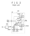
- FIG. 1 shows conventional circuitry of the PLL circuit.
- the conventional PLL circuit comprises:
- a quartz oscillator 100 which outputs a base signal fs having frequency f s [Hz];
- a divider (1/R) 200 which divides the base signal fs outputted from the quartz oscillator 100 by R and generates a reference signal fs/R;
- phase comparing detector (PD) 300 which generates voltage (phase difference signals PDU and PDD) corresponding to a phase difference between inputted two kinds of signals (the reference signal fs/R and an oscillation dividing signal f 0 /N);
- the low-pass filter (LPF) 500 which eliminates high frequency components in an output current signal Icp inputted from the charge pump circuit 400 and shapes its waveform;
- VCO voltage control oscillator 600 which oscillates according to a voltage value of a control voltage signal CC inputted from the low-pass filter 500 ;
- a programmable divider (1/N) 700 which divides an oscillation signal f 0 having frequency f 0 [Hz] outputted from the VOC 600 by N by applying dividing number N according to instructions from the outside;
- a data interface 800 which sets a dividing value N in the programmable divider 700 ;
- a lock detector circuit (LOCK) 900 which detects whether or not the two kinds of signals (the reference signal fs/R and the oscillation dividing signal f 0 /N) inputted into the phase comparing detector (PD) 300 are synchronized.
- the phase comparing detector 300 compares the reference signal fs/R having the frequency f s /R [Hz], which is outputted from the quartz oscillator 100 and divided by R in the divider 200 , with the oscillation dividing signal f 0 /N having the frequency f 0 /N [Hz], which is outputted from the voltage control oscillator 600 and divided by N in the programmable divider 700 . According to the result of the comparison, the phase comparing detector 300 outputs the phase difference signals PDU and PDD.
- the charge pump circuit 400 switches a current value I cp [Ampere] of an output current signal Icp on the basis of a fixed cycle lock signal Iosw inputted from the lock detector circuit 900 .
- the output current signal Icp turns the waveform-shaped control voltage signal CC of the voltage value CC [V] by the low-pass filter 500 . Then the output current signal Icp is inputted into the voltage control oscillator 600 .
- the PLL circuit shown in FIG. 1 executes PLL control by method of correcting the control voltage signal CC inputted into the voltage control oscillator 600 on the basis of the phase difference between the reference signal fs/R having the frequency f s /R [Hz], which is obtained by dividing the base signal fs having the frequency f s [Hz] by R, and the oscillation dividing signal f 0 /N having the frequency f 0 /N [Hz], which is obtained by dividing the oscillation signal f 0 having the frequency f 0 [Hz] outputted from the voltage control oscillator 600 by N, in the phase comparing detector 300 .
- the PLL circuit having the above configuration is importantly characterized by frequency lock-up time, that is, frequency stability time which dissolves phase difference which arises from switching channels (frequency), and a carrier noise ratio showing purity of the normal signal in the oscillation signal f 0 outputted from the voltage control oscillator 600 , that is, a C/N ratio.
- the both characteristics of the frequency lock-up time and a C/N ratio depend on damping factor in the PLL circuit.
- the damping factor is found by the current value I cp [Ampere] of the output current signal Icp from the charge pump circuit 400 , a filter constant in the low-pass filter 500 , a dividing ratio N in the programmable divider 700 and so forth.
- P-MOSFET Q 401 is set up on an input port of the phase difference signal PDU outputted from the phase comparing detector 300 .
- N-MOSFET Q 402 is set up through an inverter INV 401 on an input port of the phase difference signal PDD outputted from the phase comparing detector 300 .
- the board of the P-MOSFET Q 401 is connected to a source.
- the source is connected to a power supply voltage V through a galvano static circuit I 4002 .
- the board of the N-MOSFET Q 402 is connected to a source.
- the source is grounded through a galvano static source I 4003 .
- the charge pump circuit 400 comprises a switch SW 4010 which switches according to the lock signal Iosw outputted from the lock detector circuit 900 , a galvano static circuit I 4001 whose one side is connected to the switch SW 4010 and whose other side is grounded, and a galvano static circuit I 4000 which is set up in parallel with the switch SW 4010 and the galvano static circuit I 4001 .
- one side of the switch SW 4010 which is not connected to the galvano static circuit I 4001
- one side of the galvano static circuit I 4000 which is not grounded, are connected to the input sides of the galvano static circuits I 4002 and I 4003 , respectively.
- current passing through the galvano static circuits I 4000 and I 4001 current conducted the galvano static circuits I 4002 and I 4003 are regulated.
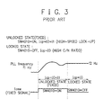
- the conventional charge pump circuit 400 operates as shown in FIG. 3. That is, in unlocked state (SW 4010 : ON) where the lock signal Iosw is inputted from the lock detector circuit 900 into the switch SW 4010 , the charge pump circuit 400 outputs current value (I 4000 +I 4001 ) calculated by adding the current I 4001 passing through the galvano static circuit I 4001 and the current I 4000 passing through the galvano static circuit I 4000 to the low-pass filter 500 as the output current signal Icp.
- the charge pump circuit 400 outputs only current value I 4000 passing through the galvano static circuit I 4000 to the low-pass filter 500 as the output current signal Icp.
- the timing of switching the output current I cp outputted from the charge pump circuit 400 is set up by applying the lock signal Iosw outputted with constant cycle from the lock detector 900 .
- the supply current during definite period of time is switched. Therefore, it is impossible to arbitrarily set up time according to a condition of the phase difference between the two kinds of signals. Consequently, setting up the filter constant in the low-pass filter 500 , which is an external filter, largely depends on the damping factor, and it is difficult to be satisfied with the lock-up time and the C/N characteristic.
- a PLL circuit comprising:
- phase comparing means which outputs phase difference signals on the basis of phase difference of inputted two signals
- a fast lock timer circuit which outputs a signal for switching a value of the output current signal outputted from the charge pump means, wherein:
- the fast lock timer circuit outputs a timer signal for lock-up or lock to the charge pump in order to switch the value of the output current signal.
- the PLL circuit switches an unlock period, which is a lock-up getting a high C/N ratio, and a lock period getting high-speed lock-up at arbitrary intervals on the basis of the output current signal.
- the PLL circuit further includes a low-pass filter and an oscillator control means, wherein the fast lock timer circuit switches the value of the output current signal from the charge pump circuit at arbitrary intervals by counting a base signal divided according to an inputted dividing ratio setting data and gets speeding up of lock-up time and a high C/N ratio characteristic.
- the PLL further includes:
- a data interface means which directs the fast lock timer means to switch the value of the output current signal on the basis of inputted data
- a voltage control oscillation means which outputs an oscillation signal on the basis of an oscillator control signal outputted from the low-pass filter
- the fast lock timer means outputs a signal for switching the value of the output current value on the basis of the direction.
- the fast lock timer further includes a filter switching means which outputs a signal for switching prescribed loop-bandwidth in the low-pass filter;
- the low-pass filter includes a first filter means and a second filter means which are connected in parallel, wherein the signal outputted from the filter switching means is inputted into an input port of the second filter through a first resistor, the second filter means includes the first resistor, a second resistor and a capacitor, the first and second resistors are connected in parallel with the first filter means through the capacitor, the first and second resistors are connected to the capacitor in parallel, and the second resistor is grounded, besides it is preferable that:
- the filter switching means switches the prescribed loop-bandwidth according as the current value of the output current signal is switched
- the data interface means includes:
- a shift register receiving a clock signal and synchronizing with an externally signal, inputting a data signal on the basis of the synchronization, and outputting the inputted data signal to the fast lock timer means;
- an enable counter specifying at least one part of the data signal outputted from the shift register, and further outputting a latch/reset signal which specifies a timing of switching value of the output current signal;
- the fast lock timer means includes:
- a data latch means latching the inputted data signal on the basis of the latch/reset signal outputted form the enable counter means, and outputs at least one count value setting signal;
- a programmable counting means setting the count value on the basis of the at least one count value setting signal, counts a reference signal till the count value setting a start point as an input of the latch/reset signal, and outputs the timer signal for switching the current value of the output current signal until cycles of the count value are counted;
- the programmable counter has three inputs and one output, in which two inputs among the three inputs are for an enable signal input and the divided base signal input, including:
- a first NAND circuit and a second inversion circuit set up on an input port of the divided base signal through a first inversion circuit, wherein:
- the one output includes a third NAND circuit into which all ⁇ overscore (Q) ⁇ outputs of the flip-flops are inputted;
- the enable signal and a branching signal of the divided base signal are inputted into each input of the pairs of NAND circuits, the signal from the data latch is inputted into the one NAND circuit forming each pairs of NAND circuits, and each output from the one NAND circuit forming each pairs of NAND circuits is inputted into remaining NAND circuits forming the pairs of NAND circuits;
- each of the output from the one NAND circuit forming the pairs of NAND circuits branches, which is inputted into each ⁇ overscore (S) ⁇ in the flip-flops, each of the ⁇ overscore (Q) ⁇ outputs is branched, and the branched ⁇ overscore (Q) ⁇ output is inputted into each D in the flip-flops, each of the remaining ⁇ overscore (Q) ⁇ outputs is inputted into each Cp in a post flip-flop through a second NAND circuit in a second stage and a fourth inversion circuit in a fourth stage, the divided base signal from the first NAND circuit and the second inversion circuit is inputted into a CP in a flip flop in a first stage through a third inversion circuits and a fourth inversion circuit in a fourth stage, which is set in a post stage of the third inversion circuit; and
- the flip-flop circuits are set/reset-D-flip-flops.
- the charge pump includes a switch comprising an N-MOSFET
- the timer signal is inputted into a gate of the N-MOSFET
- the charge pump includes the switch and connected two galvano static circuits in parallel;
- one of the two-galvano static circuits is connected to the switch in series;
- the switch outputs current through at least one of the galvano static circuits on the basis of the timer signal.
- phase comparing means includes:
- a second NAND circuit whose input side is connected to each output port of the first NAND circuits and each output port of reset/set-flip-flops;
- a plurality of third NAND circuits whose input sides are connected to each output port of the first NAND circuits, each output port of the reset/set-flip-flops, and an output port of the second NAND circuit, wherein:
- each output port of the third NAND circuits is connected to each input port of the first NAND circuits
- the dividing ratio setting data applied in this kind of PLL circuit includes:
- reset or latch for switching frequency of the base signal is specified on the basis of the enable signal.
- FIG. 1 is a block diagram showing a configuration of a conventional PLL circuit
- FIG. 2 is a circuit diagram showing circuitry of a conventional charge pump circuit 400 ;
- FIG. 3 is a timing chart showing time and motion of each signal in the conventional PLL circuit
- FIG. 4 is a block diagram showing a configuration of a PLL circuit according to a first embodiment of the present invention
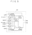
- FIG. 5 is a circuit diagram showing circuitry of a generally applied phase comparing detector 1 ;
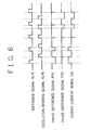
- FIG. 6 is a timing chart showing phase difference signals PDU and PDD, which are outputted from the phase comparing detector 1 shown in FIG. 5 when a reference signal fs/R and an oscillation dividing signal f 0 /N are inputted into the phase comparing detector 1 , and an output current signal Icp, which is outputted from a charge pump circuit 2 ;
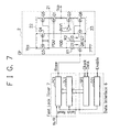
- FIG. 7 is a circuit diagram showing circuitry of the charge pump circuit 2 according to the first embodiment of the present invention.
- FIG. 8 is a circuit diagram showing an example of circuitry of a programmable counter PC 1 configuring a fast lock timer circuit 7 according to the first embodiment of the present invention
- FIG. 9 is a timing chart showing time and motion of each signal according to the first embodiment of the present invention.
- FIG. 13 is a block diagram showing a PLL circuit according to a second embodiment of the present invention.
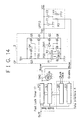
- FIG. 14 is a circuit diagram showing circuitry of a charge pump circuit 2 , low-pass filter 13 and fast lock timer circuit 17 according to the second embodiment of the present invention.
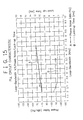
- FIG. 15 is a graph showing phase noise characteristic and lock-up time dependence for frequency of loop-bandwidth.
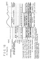
- FIG. 16 is a timing chart showing time and motion of each signal according to the second embodiment of the present invention.
- a PLL circuit which switches current supply from a charge pump circuit (CP) to a low-pass filter (LPF), is characterized by setting up a fast lock timer circuit that switches the current before and after a phase of an input signal (hereinafter referred to as a base signal) and a phase of a signal oscillated by a voltage control oscillator (VCO) in the PLL circuit are synchronized (locked in).
- CP charge pump circuit
- LPF low-pass filter
- the PLL circuit counts the base signal, which is divided by R (R is a fixed dividing ratio), at arbitrary dividing number. Thereby, it becomes possible to switch the output current from the charge pump circuit at arbitrary time, supply sufficient current to the low-pass filter set up in the post stage of the fast lock timer at lock-up, and supply sufficient current to the low-pass filter at locked.
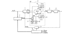
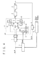
- FIG. 1 is a block diagram showing configuration of a PLL circuit according to the first embodiment of the present invention.
- a PLL circuit of the present invention comprises:
- phase comparing detector (PD) 1 which compares phases of inputted two kinds of signals and outputs voltage as phase difference signals PDU and PDD on the basis of the result of the above comparison;
- a charge pump circuit (CD) 2 which outputs output current signal Icp having various current value on the basis of the signals PDU and PDD inputted from the phase comparing detector 1 ;
- a low-pass filter (LPF) 3 which eliminates high frequency components in the output current signal Icp outputted from the charge pump circuit 2 by an integral process, shapes its waveform into direct current (DC) components, and outputs the waveform-shaped signal Icp as an oscillator control signal CC;
- VCO voltage control oscillator
- a programmable divider (1/N) 5 which divides the oscillation signal f 0 inputted from the voltage control oscillator 4 by N by applying externally inputted arbitrary dividing number N;
- a data interface 6 which sets up the externally directed dividing number N to the programmable divider 5 ;
- a fast lock timer circuit 7 which converts the current value of the output current signal Icp outputted from the charge pump circuit 2 on the basis of an externally directed count value M.
- the two kinds of signals means a reference signal fs/R having frequency f s /R [Hz], which is found by dividing a base signal fs having frequency f s [Hz] inputted from the outside of the PLL circuit shown in FIG. 4 by dividing number R, and an oscillation dividing signal f 0 /N having frequency f 0 /N [Hz], which is outputted from the programmable divider 5 .
- the phase comparing detector 1 compares a phase of the reference signal fs/R and that of the oscillation dividing signal f 0 /N. On the basis of the result of the comparison, the phase comparing detector 1 outputs the phase difference signals PDU and PDD.
- the phase comparing detector 1 applied in this embodiment comprises nine NAND gates NAND 1 to NAND 9 .
- the phase comparing detector 1 applied in this embodiment may be the one which is generally applied.
- the NAND gates NAND 2 and NAND 3 , and NAND 4 and NAND 5 form reset/set-flip-flops R-S-FF 1 and R-S-FF 2 , respectively.
- R-S-FF 1 and R-S-FF 2 reset/set-flip-flops
- Chattering means noise voltage generated at switching a low level “L” (namely, and a high level “H” each other in the case where machinelike contact points are applied. This kind of chattering causes malfunction at switching.
- the phase comparing detector 1 applied in the present invention can eliminate the chattering generated when positive and negative of the two kinds of the inputted signals (fs/R and f 0 /N) counterchanges by applying the four NAND gates NAND 2 to NAND 5 connected as a reset/set-flip-flop type, respectively.
- the two input ports of the NAND gate NAND 7 are connected to the output ports of the NAND 1 and NAND 6 , respectively.
- the other two ports are connected to the output ports of the R-S FF 1 and R-S FF 2 , respectively.
- the output port of the NAND 7 is connected to the input ports of the NAND 8 and NAND 9 , and the R-S-FF 1 and R-S-FF 2 .
- the output ports of the NAND 8 and NAND 9 are connected to the input ports of the NAND 1 and NAND 6 , respectively.
- phase difference signals PDU and PDD outputted from the phase comparing detector 1 shown in FIG. 5 comes to the ones shown in FIG. 6.
- the outputted phase difference signals PDU and PDD are inputted into the charge pump circuit 2 , respectively as shown in FIG. 4.
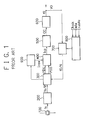
- the charge pump circuit 2 applied in the present invention comprises an inverter INV 1 set up on the output port of the phase difference signal PDD, and further comprises a P-MOSFET Q 1 , a N-MOSFET Q 2 , galvano static circuits I 0 , I 1 , I 2 and I 3 , and a switch SW 1 .
- FIG. 7 A circuit example of the charge pump circuit 2 having the above configuration is shown in FIG. 7 in detail.
- the P-MOS type FET Q 1 is set up on the input port of the phase difference signal PDU.
- the inverter INV 1 is set up on the input port of the phase difference signal PDD.
- the charge pump circuit 2 applied in this embodiment further comprises three P-MOSFETs Q 3 , Q 4 and Q 5 , three N-MOSFETs Q 6 , Q 7 and Q 8 , and resistors R 1 and R 2 .
- the P-MOSFET Q 1 and the N-MOSFET Q 2 constitute a C-MOS type impedance transformation circuit 21 , whose drains are connected each other.
- impedance transformation circuit 21 input impedance is practically infinite.
- output impedance is switched at ON (continue)/OFF (shutdown) state.
- the drain of the P-MOSFET Q 4 constituting the galvano static circuit 22 is connected to the gates of the N-MOSFETs Q 6 and Q 7 , which constitute a galvano static circuit 23 , and the drain of the N-MOSFET Q 7 .
- the galvano static circuit 23 corresponds to the galvano static circuit I 3 shown in FIG. 4.
- the galvano static circuit 23 also serves as a load resistance of the above described impedance transformation circuit 21 and serves as output impedance when the N-MOSFET Q 6 is on state, which operates in order to supply constant current in outputting.
- the N-MOSFET Q 8 constitutes the switch SW 1 shown in FIG. 4.
- a timer signal flosw is inputted from the external fast lock timer 7 into the N-MOSFET Q 8 , it comes to on state wherein current is passed through the resistor R 1 .
- the resistors R 1 and R 2 constitutes the galvano static circuit I 0 and I 1 shown in FIG. 4, respectively.
- Current I 1 passes through the resistor R 1 and I 0 passes through R 2 , respectively.
- phase difference signal PDU When the phase difference signal PDU is inputted from the phase difference detector PD 1 , the charge pump circuit 2 operates so as to output positive current. On the other hand, when the phase difference signal PDD is inputted, the charge pump circuit 2 operates in order to outputs negative current.
- the current value of the output current signal Icp outputted from the charge pump circuit 2 is the sum of the current passing through the resistors R 1 and R 2 (I 0 +I 1 ).
- the current value of the output current signal Icp outputted from the charge pump circuit 2 is the negative value of the sum of the current passing through the resistors R 1 and R 2 ( ⁇ (I 0 +I 1 )).
- phase comparing detector 1 The two kinds of signals inputted into the phase comparing detector 1 are shown as the reference signal fs/R and the oscillation dividing signal f 0 /N for convenience of explanation.
- the phase difference signal PDU outputted from the phase comparing detector 1 gets down at the timing when the reference signal fs/R rises, and shows a “L” (low) level only during a time corresponding to the phase difference thereof.
- the phase difference signal PDD keeps an “H” (high) level.
- the phase difference signal PDD outputted from the phase comparing detector 1 gets down at the timing when the oscillation dividing signal f 0 /N rises, and shows the “L” level only during a time corresponding to the phase difference thereof.
- the phase difference signal PDU keeps the “H” level.
- both of the phase difference signals PDU and PDD show the “H” level, which shows a state where the PLL is locked.
- the phase difference signal PDU is inputted into the gate of the P-MOSFET Q 1 in the charge pump circuit 2 .
- the phase difference signal PDD after the voltage level thereof is inverted at the inverter INV 1 , is inputted into the gate of the N-MOFET Q 2 .
- phase difference signal PDU By inputting the phase difference signal PDU into the gate, when the phase difference signal PDU is on the “L” level, that is, when the phase of the oscillation dividing signal f 0 /N lags that of the reference signal fs/R, the P-MOSFET Q 1 in the charge pump circuit 2 comes to on state and outputs the current supplied from the galvano static circuit 12 as the output current signal Icp.
- phase difference signal PDD is on the “L” level, that is, when the phase of the reference signal fs/R lags that of the oscillation dividing signal f 0 /N
- the N-MOSFET Q 2 in the charge pump circuit 2 comes to on state and outputs the current supplied from the galvano static circuit I 3 as the output current I cp .
- the current supplied from the galvano static circuit 13 is negative current. Therefore, as shown in FIG. 6, the output current signal Icp outputted from the charge pump circuit 2 is positive one when the P-MOSFET Q 1 is in on state. On the other hand, the output signal Icp is negative one when the N-MOSFET Q 2 is in on state.
- the outputted output current signal Icp is inputted into the low-pass filter 3 , and an integral process is executed to the signal.
- the integral process the high frequency components in the output current signal Icp are eliminated, whose waveform is shaped into direct current components, and outputted as oscillator control signal CC whose voltage level is CC [V].
- the oscillation signal f 0 outputted from the voltage control oscillator 4 is based on the phase difference between the two kinds of signals from the phase comparing detector 1 .
- the oscillation signal f 0 outputted from the voltage control oscillator 4 is inputted into the programmable divider 5 .
- the programmable divider 5 decides the dividing number N by a signal inputted from the data interface 6 , and divides the oscillation signal f 0 by N. Therefore, the phase comparing detector 1 is configured so as to compare the reference signal fs/R found by dividing the base signal fs by R and the oscillation dividing signal f 0 /N found by dividing the oscillation signal f 0 by N. This shows that the frequency ratio between the two kinds of signals, which are synchronized practically, comes to N/R in the PLL circuit according to this embodiment.
- FIG. 7 shows a configuration of the data interface 6 .
- the data interface 6 applied in this embodiment comprises a shift register SR 1 and an enable counter EC 1 .
- a clock signal Clock and data signals Data are inputted to the shift register SR 1 .
- An enable signal Enable is inputted into the enable counter (EC 1 ).
- the dividing number N and the count value M set up in the programmable divider 5 and the fast lock timer circuit 7 by these dividing ratio setting data are arbitrary number and value. These number and value may be set up on the basis of the result of monitoring frequency outputted from the PLL circuit applied in this embodiment, or may be set up according to conditions beforehand.
- the above-described dividing ratio setting data comprises the clock signal Clock for bit synchronization between the data interface 6 and the external configuration, the data signals (signal) consisting of serial data with k bit, and the enable signal Enable specifying available components of the data signals.
- the shift register SR 1 operates so as to find out the bit synchronization with outside on the basis of the externally inputted clock signal Clock and input the data signals Data according to the synchronization. In parallel with the operation, the shift register SR 1 operates so as to judge the available components in the inputted data signals Data according to the enable signal Enable inputted into the enable counter EC 1 , and so as to decide the dividing number N that are to be set up in the programmable divider 5 .
- the data interface 6 picks up data for setting up the dividing number N in the programmable divider 5 and data for setting up the count value M in the fast lock timer circuit 7 from the data signals Data received by the shift register SR 1 in the fast clock timer circuit 7 , and outputs each data to the programmable divider 5 and the fast lock timer 7 shown in FIG. 4.
- the data interface 6 outputs the enable signal Enable received by the enable counter EC 1 to the above-described programmable divider 5 and the fast lock timer circuit 7 as a latch signal Latch or a reset signal Reset.
- the dividing number N of the oscillation dividing signal f 0 /N is set up in the programmable divider 5 applied in this embodiment.
- the count value M of the reference signal fs/R is set up in the fast lock timer circuit 7 as described later.
- the dividing number N set up in the programmable divider 5 and the count value M set up in the fast lock timer circuit 7 are both found on the basis of the same dividing ratio setting data.
- this embodiment there is shown a configuration that a data area for setting up the dividing number N and a data area for setting up the count value M have different bit area, respectively.
- This kind of data “bit” configuration is often applied in prior arts. Thereby, the explanation of the data configuration in this embodiment will be abbreviated.
- the current level of the output current signal Icp outputted from the charge pump 2 is switched at frequency pulling-in (unlocked state) and when it is in phase (at locked state). In other wards, at unlocked (lock-up) state, relatively high current is run out from the charge pump circuit 2 . On the other hand, at locked state, relatively low current is run out. By this configuration, it becomes possible to cut down lock-up time and gain high C/N characteristic.
- the fast lock timer circuit 7 is newly set up in the PLL circuit in the first embodiment.
- the fast lock timer circuit 7 comprises a data latched circuit DL 1 and a programmable counter PC 1 .
- the data latch circuit DL 1 stores the dividing ratio setting data inputted from the data interface 6 .
- the programmable counter PC 1 consists of n bit, stores data (dividing ratio setting data) latched by the data latch circuit DL 1 , and sets up the count value M on the basis of the stored data.
- the first lock timer circuit 7 receives the latched data Latch outputted from the shift register SR 1 in the data interface 6 at the data latch circuit DL 1 . On the basis of the latched data, the fast lock timer circuit 7 operates so as to get the programmable counter PC 1 to count the inputted reference signal fs/R.
- the signal Enable inputted into the enable counter EC 1 functions as the latch signal Latch specifying the available components in the latch data, which is sent to the data latch circuit DL 1 , and the reset signal Reset resetting the count value M set up in the programmable counter PC 1 , which is sent to the programmable counter PC 1 .
- a signal setting up the count value M in the programmable counter PC 1 which is outputted from the above-described data latch circuit DL 1 , is shown as a count value setting signal FLK as described later.
- the maximum count value set up in the programmable counter PC 1 is set up as “15”. Therefore, in this embodiment, there is an explanation that the count value setting signal FLK is shown as the count value setting signals FLK 1 to FLK 4 .
- the programmable counter PC 1 configuring the above-described fast lock timer circuit 7 by using FIG. 8.
- the programmable counter PC 1 applied in this embodiment has two input signals.
- the enable signal Enable as the reset signal is inputted into one, and the reference signal fs/R, which is a target of the count, is inputted into the other.
- the reference signal fs/R inputted as above branches One of the branching signals is inputted into an inverter INV 10 , and the rest of the branching signal is inputted into NAND circuits NAND 16 to NAND 23 , respectively.
- the reference signal fs/R of the branching signal inputted into the inverter INV 10 is inputted into an inverter INV 11 through the NAND circuit NAND 10 . After that, the reference signal fs/R outputted from the inverter INV 11 branches the following four signals as shown in FIG. 8.
- the first signal is inputted into a Cp input in a set/reset-D-flip-flop SR-D-FF 1 through inverters INV 12 and INV 13 .
- the second signal is inputted into a Cp input in a set/reset-D-flip-flop SR-D-FF 2 through an inverter INV 14 after a NAND circuit NAND 13 calculates a logical product between the second signal and a ⁇ overscore (Q) ⁇ output in the set/reset-D-flip-flop SR-D-FF 1 .
- the third signal is inputted into a Cp input in a set/reset-D-flip-flop SR-D-FF 3 through an inverter 15 after a NAND circuit NAND 14 calculates a logical product between the third signal and ⁇ overscore (Q) ⁇ outputs in the set/reset-D-flip-flop SR-D-FF 1 and the set/reset-D-flip-flop SR-D-FF 2 .
- the fourth signal is inputted into a Cp input in a set/reset-D-flip-flop SR-D-FF 4 through an inverter 16 after a NAND circuit NAND 15 calculates a logical product between the fourth signal and ⁇ overscore (Q) ⁇ outputs in the set/reset-D-flip-flop SR-D-FF 1 , set/reset-D-flip-flop SR-D-FF 2 and set/reset-D-flip-flop SR-D-FF 3 .
- the enable signal Enable is inputted into the NAND circuits NAND 16 to NAND 23 , respectively as well.
- the count value setting signals FLK 1 , FLK 2 , FLK 3 and FLK 4 outputted from the data latch circuit DL 1 are inputted into the NAND circuits NAND 16 , NAND 18 , NAND 20 , and NAND 22 , respectively in the above configuration.
- the count value setting signals FLK 1 , FLK 2 , FLK 3 and FLK 4 outputted from the data latch circuit DL 1 are the signals Data that the data signals, which are received through the shift register SR 1 in the data interface 6 by the data latch circuit DL 1 , are latched, respectively.
- the latched data signals are inputted into the programmable counter PC 1 as described above as the count value setting signals FLK 1 to FLK 4 through leased lines (buses).
- the maximum count value set up as the count value M is set up as “15”, and the programmable counter PC 1 is configured so that the count value M comes to natural numbers from “1” to “15” by the count value setting signals FLK 1 to FLK 4 .
- the count value setting signal FLK 1 when “1” is inputted as the count value setting signal FLK 1 , “1” is added to a count number m.
- the count value setting signal FLK 2 When “1” is inputted as the count value setting signal FLK 2 , “2” is added to the count number m.
- “4” is added to the count number m.
- the count number m set up in the programmable counter PC 1 is set up so that the count value M comes to natural numbers from “1” to “15” by the combination of these added values.
- the count value M is set up as “1” is inputted into the count value setting signal FLK 1 only.
- “1” is inputted into all of the count value setting signals FLK 1 to FLK 4 .
- each of the signals outputted form the NAND circuits NAND 16 , NAND 18 , NAND 20 and NAND 22 is inverted and inputted into each of the S inputs in the set/reset-D-flip-flops SR-D-FF 1 to SR-D-FF 4 connected thereto, respectively.
- each of the signals outputted form the NAND circuits NAND 17 , NAND 19 , NAND 21 and NAND 23 is inverted and inputted into each of the R inputs in the set/reset-D-flip-flops SR-D-FF 1 to SR-D-FF 4 connected thereto, respectively.
- each of the signals outputted form the inverters INV 13 , INV 14 , INV 15 and INV 16 is inputted into each of the Cp inputs in the set/reset-D-flip-flops SR-D-FF 1 to SR-D-FF 4 .
- each of the D inputs in the same set/reset-D-flip-flops SR-D-FF 1 to SR-D-FF 4 is connected to each of the ⁇ overscore (Q) ⁇ outputs in the same set/reset-D-flip-flops SR-D-FF 1 to SR-D-FF 4 .
- Each of the ⁇ overscore (Q) ⁇ outputs is inputted into each of the D inputs.
- a NAND circuit NAND 11 calculates the logical product of the signals outputted from each of the ⁇ overscore (Q) ⁇ outputs in each of the same set/reset-D-flip-flops SR-D-FF 1 to SR-D-FF 4 . Then, the inverted value of the logical product is outputted as the output signal (timer signal) flosw from the fast lock timer circuit 7 as shown in FIG. 8.
- the programmable counter PC 1 counts the number of the rise of the reference signal fs/R by setting the start point as the rise of the enable signal Enable inputted from the data interface 6 . Then the timer signal flosw is outputted to the charge pump circuit 2 until the number of the rise arrives at the set-up count number m.
- the timer signal flosw is inputted into the gate of the N-MOSFET Q 8 consisting of the switch SW 1 .
- the absolute value of the current of the output current signal Icp outputted from the charge pump circuit 2 comes to
- the current value I cp [Ampere] of the output current signal Icp outputted from the charge pump circuit 2 is switched synchronizing with the timer signal flosw outputted from the fast lock timer circuit 7 .
- the current I cp [Ampere] supplied from the charge pump circuit 2 to the low-pass filter 3 is set to large value. Thereby, it becomes possible to cut down the lock-up time.
- the timer signal is on the low level
- the current I cp [Ampere] supplied from the charge pump circuit 2 to the low-pass filter 3 is set to small value. Thereby, is becomes possible to get high C/N characteristic.
- FIG. 9 is a timing chart showing time and motion of operation of each signal in the first embodiment.
- PLL Frequency indicates the frequency of a base signal fs.
- the channel frequency to which a PLL circuit is to be tuned namely, the channel frequency of a reference signal fs/R, which is obtained by dividing a base signal fs by R, is switched from f 1 [Hz] to f 2 [Hz].
- “Conventional CP Current Condition” shown in FIG. 9 indicates a transition in current values of a signal outputted from the charge pump circuit 400 of the PLL circuit shown in FIG. 1.
- the PLL circuit is switched to an unlocked state.
- relatively high electrical current is outputted from the charge pump circuit 400 so that current value of a signal outputted from the charge pump circuit 400 is to be restricted after the PLL circuit enters into a locked state. Therefore, in the structure of the conventional PLL circuit, a relatively high electrical current is supplied to the LPF 500 even at the stage immediately before the lock-up converges on a stable state, and thus high-speedability in lock-up time is hindered.
- “Data”, “Clock” and “Enable” shown in FIG. 9 are included in dividing ratio setting data inputted from an external device as is explained above. Those are signals for deciding a dividing number (dividing ratio) N for the programmable divider 5 and a count value M for the fast lock timer circuit 7 in FIG. 4.
- the data signal Data is inputted to the data interface 6 shown in FIG. 4 from an external device simultaneously with the clock signal Clock before the process for switching the channel frequency, to which a PLL circuit is to be tuned, from f 1 [Hz] to f 2 [Hz].
- the dividing number N and the count value M set at the programmable divider 5 and the fast lock timer circuit 7 become effective at the point of time when an enable signal Enable is inputted to respective circuits (the programmable divider 5 and the fast lock timer circuit 7 ) from the data interface 6 afterwards. Thereby dividing of the oscillation signal f 0 and count of the reference signal fs/R are commenced at the programmable divider 5 and the fast lock timer circuit 7 , respectively.
- FIG. 9 the dividing number N and the count value M set at the programmable divider 5 and the fast lock timer circuit 7 become effective at the point of time when an enable signal Enable is inputted to respective circuits (the programmable divider 5 and the fast lock timer circuit 7 ) from the data interface 6 afterwards.
- dividing of the oscillation signal f 0 and count of the reference signal fs/R are commenced at the programmable divider 5 and the fast lock timer circuit 7 , respectively.
- the timing of inputting the enable signal Enable to the programmable counter PC 1 is synchronized with the timing of switching the frequency that the oscillation signal f 0 has to lock from F 1 [Hz] to F 2 [Hz]. Accordingly, the charge pump circuit 2 of the first embodiment can switch the current value of an output current signal Icp simultaneously with the timing in which the frequency of the oscillation signal f 0 is switched.
- the fast lock timer circuit 7 After the count value M is set up, the fast lock timer circuit 7 outputs a timer signal flosw to a switch SW 1 of the charge pump circuit 2 until the count number m of the reference signal fs/R comes to the count value M set as above. Thereby the current value of an output current signal Icp fed to the LPF 3 from the charge pump circuit 2 is switched to a relatively large value (
- SR-D-FF 1 ⁇ overscore (Q) ⁇ ”, “SR-D-FF 2 ⁇ overscore (Q) ⁇ ”, “SR-D-FF 3 Q”, and “SR-D-FF 4 ⁇ overscore (Q) ⁇ ” in FIG. 9 are output signals from ⁇ overscore (Q) ⁇ outputs of set/reset-D-flip-flops constituting the programmable counter PC 1 of the fast lock timer circuit 7 .
- the set/reset-D-flip-flops SR-D-FF 1 to SR-D-FF 4 that constitute the programmable counter PC 1 operate based on purposes according to data signals (referred to as signals FLK 1 to FLK 4 in the present embodiment) outputted from the data latch circuit DL 1 in the fast lock timer circuit 7 . That is, for the programmable counter PC 1 of the present embodiment, the count value setting signal FLK 4 needs to be inputted as “1”, and the other count value setting signals FLK 1 to FLK 3 need to be inputted as “0”. Accordingly, the count value M is set to “8” at the programmable counter PC 1 . The operation for setting the count value M will be explained below by referring to FIG. 10.
- FIG. 10 it is provided to explain an operation example in this embodiment that, with respect to the signals FLK 1 to FLK 4 outputted from the data latch circuit DL 1 , the respective signals FLK 1 to FLK 3 are low-level signals (“0”), and the signal FLK 4 is a high-level signal (“1”).
- NAND circuits NAND 16 , NAND 18 and NAND 20 output “1” in every period.
- a NAND circuit NAND 22 outputs “0” in a period when a reference signal fs/R as well as the reset signal Reset are “1”, and outputs “1” in other periods.
- NAND circuits NAND 17 , NAND 19 and NAND 21 output “0” in a period when a reference signal fs/R as well as the reset signal Reset are “1”, and output “1” in other periods.
- a NAND circuit NAND 23 outputs “1” in every period.
- each of the ⁇ overscore (S) ⁇ inputs and ⁇ overscore (R) ⁇ inputs has a NAND circuit at its gate, where an inputted signal is inverted on the occasion of reception.
- ⁇ overscore (S) ⁇ inputs are “1” for during a period when a reference signal fs/R as well as the reset signal Reset are “1”, and “0” in other periods.
- the NAND circuit NAND 13 derives the logical product of the output signal “SRD-FF 1 ⁇ overscore (Q) ⁇ ” from the ⁇ overscore (Q) ⁇ output of the set/reset-D-flip-flop SR-D-FF 1 and the reference signal fs/R.
- the “SRD-FF 1 ⁇ overscore (Q) ⁇ ” is then inputted to a Cp input of the set/reset-D-flip-flop SR-D-FF 2 as a strobe signal via an inverter INV 14 . This signal corresponds to “INV 14 ” in FIG. 10.
- the set/reset-D-flip-flop SR-D-FF 2 switches a signal “SRD-FF 2 ⁇ overscore (Q) ⁇ ” to be outputted from the ⁇ overscore (Q) ⁇ output from “1” to “0”, or from “0” to “1” according to the down edge of the signal “INV 14 ”.
- the NAND circuit NAND 14 obtains the logical product of the signal “SRD-FF 2 ⁇ overscore (Q) ⁇ ” outputted in this manner, the reference signal fs/R and the signal “SRD-FF 1 ⁇ overscore (Q) ⁇ ”. Subsequently, the signal “SRD-FF 2 ⁇ overscore (Q) ⁇ ” is inputted to a Cp input as a strobe signal for the set/reset-D-flip-flop SR-D-FF 3 via an inverter INV 15 . This signal corresponds to “INV 15 ” in FIG. 10.
- the set/reset-D-flip-flop SR-D-FF 3 switches a signal “SRD-FF 3 ⁇ overscore (Q) ⁇ ” to be outputted from the ⁇ overscore (Q) ⁇ output from “1” to “0”, or from “0” to “1” according to the down edge of the signal “INV 15 ”.
- the NAND circuit NAND 15 obtains the logical product of the signal “SRD-FF 3 ⁇ overscore (Q) ⁇ ” outputted as above, the reference signal fs/R, and the signals “SRD-FF 1 ⁇ overscore (Q) ⁇ ” and “SRD-FF 2 ⁇ overscore (Q) ⁇ ” outputted from the ⁇ overscore (Q) ⁇ each of the set/reset-D-flip-flops SR-D-FF 1 and SR-D-FF 2 , respectively.
- the signal “SRD-FF 3 ⁇ overscore (Q) ⁇ ” is supplied to a Cp input as a strobe signal of the set/reset-D-flip-flop SR-D-FF 4 via an inverter INV 16 .
- This signal corresponds to “INV 16 ” in FIG. 10.
- the set/reset-D-flip-flop SR-D-FF 4 switches a signal “SRD-FF 4 ⁇ overscore (Q) ⁇ ” to be outputted from the ⁇ overscore (Q) ⁇ output from “1” to “0”, or from “0” to “1” according to the down edge of the signal “INV 16 ”.
- the signals “SRD-FF 1 ⁇ overscore (Q) ⁇ ” to “SRD-FF 4 ⁇ overscore (Q) ⁇ ” outputted from the respective set/reset-D-flip-flops are inputted to the NAND circuit NAND 11 to obtain the logical product of the respective signals, which is then outputted as a timer signal flosw being an output of the fast lock timer circuit 7 .
- the logical product of the signals “SRD-FF 1 ⁇ overscore (Q) ⁇ ” to “SRD-FF 4 ⁇ overscore (Q) ⁇ ” is “0”, namely, a period of cycle time of the reference signal fs/R multiplied by 8 (or a period of 8 cycles). Therefore, the inverted value of this is “1”, namely, a period of cycle time of the reference signal fs/R multiplied by 8.
- CP current Condition a transition in current values of the output current signal Icp outputted from the charge pump circuit 2 is indicated by “CP current Condition” in FIG. 9.
- the data interface 6 decides a dividing number N and a count value M to be set at the programmable divider 5 and the fast lock timer circuit 7 , respectively based on an inputted data signal, and outputs the decided dividing number N to the programmable divider 5 and the fast lock timer circuit 7 .
- the fast lock timer circuit 7 where the count value M is set as above, initializes the count number m in the programmable counter PC 1 in response to the rising edge of an enable signal that is inputted from the enable counter EC 1 of the data interface 6 to newly commence a count. Subsequently, the fast lock timer circuit 7 outputs a timer signal flosw until “M” cycles of the reference signal fs/R are counted.
- signals inputted to the ⁇ overscore (S) ⁇ inputs of the set/reset-D-flip-flops SR-D-FF 2 to SR-D-FF 4 namely, signals outputted from the NAND circuits NAND 18 , NAND 20 and NAND 22 are “1” in every period.
- a signal inputted to the ⁇ overscore (R) ⁇ input of the set/reset-D-flip-flop SR-D-FF 1 namely, the signal outputted from the NAND circuit NAND 17 is “0” during a period when a reference signal fs/R as well as a reset signal Reset are being inputted, and “1” in other periods.
- signals inputted to the ⁇ overscore (R) ⁇ inputs of the set/reset-D-flip-flops SR-D-FF 2 to SR-D-FF 4 namely, signals outputted from the NAND circuits NAND 19 , NAND 21 and NAND 23 are “1” in every period.
- an output signal “SRD-FF 1 ⁇ overscore (Q) ⁇ ” outputted from the ⁇ overscore (Q) ⁇ output of the set/reset-D-flip-flop SR-D-FF 1 is fixed to “0” according to the event that the signal inputted to the S input becomes “1”.
- output signals “SRD-FF 2 ⁇ overscore (Q) ⁇ ” to “SRD-FF 4 ⁇ overscore (Q) ⁇ ” outputted from the ⁇ overscore (Q) ⁇ outputs of the respective set/reset-D-flip-flops SR-D-FF 2 to SR-D-FF 4 are fixed to “1” according to the event that the signals inputted to the R input becomes “1”.
- the signal outputted from ⁇ overscore (Q) ⁇ output of the set/reset-D-flip-flop SR-D-FF 1 is inverted to “1” in response to the inverter INV 13 , namely, the rising of the reference signal fs/R.
- the “SRD-FF 1 ⁇ overscore (Q) ⁇ ” is inputted to the Cp input of the set/reset-D-flip-flop SR-D-FF 2 as a strobe signal (output of the inverter INV 14 ).
- an input of the Cp input of the set/reset-D-flip-flop SR-D-FF 2 that is, a signal “INV 14 ” outputted from the inverter INV 14 is “0” in every period, and therefore, the signal “SRD-FF 2 ⁇ overscore (Q) ⁇ ” outputted from the ⁇ overscore (Q) ⁇ output of the set/reset-D-flip-flop SR-D-FF 2 is fixed to “1” and unchanged.
- signals inputted to the S inputs of the set/reset-D-flip-flops SR-D-FF 1 to SR-D-FF 4 namely, signals outputted from the NAND circuits NAND 16 , NAND 18 , NAND 20 and NAND 22 are “1” during a period when a reference signal fs/R is “1” while a reset signal Reset is being inputted, and “0” in other periods.
- signals inputted to the ⁇ overscore (R) ⁇ inputs of the set/reset-D-flip-flops SR-D-FF 1 to SR-D-FF 4 namely, signals outputted from the NAND circuit NAND 17 , NAND 19 , NAND 21 and NAND 23 are “1” in every period.
- signals recognized at the respective ⁇ overscore (S) ⁇ inputs and ⁇ overscore (R) ⁇ inputs of the set/reset-D-flip-flops SR-D-FF 1 to SR-D-FF 4 are inverted as shown in FIG. 12 by inverters that are disposed at gates of the respective inputs.
- signals outputted from the respective ⁇ overscore (Q) ⁇ outputs of the set/reset-D-flip-flops SR-D-FF 1 to SR-D-FF 4 are also determined by the same operation as above.
- lock-up time is shortened in a period while a timer signal flosw is on a high level. Besides, a high C/N ratio is achieved in a period while a timer signal flosw is on a low level.
- a channel setting for the frequency of the oscillation signal f 0 to which the PLL circuit is to be tuned is switched from f 1 [Hz] to f 2 [Hz].
- the fast lock timer circuit 7 resets a count number m of the programmable counter PC 1 in synchronization with the switching timing according to the rising of an inputted enable signal Enable, and thereby starts a new count.
- the fast lock timer circuit 7 switches the level of the timer signal flosw to a low level to shut off the switch SW 1 at the charge pump circuit 2 .
- the current value I cp [Ampere] of an output current signal Icp outputted from the charge pump circuit 2 is changed to a relatively small value. Consequently, the dumping factor of the whole PLL circuit is changed to a relatively small value and the PLL circuit operates so as to keep a stable state, thus enabling an improvement of the C/N characteristic of the whole PLL circuit.
- a PLL circuit according to the present embodiment is capable of changing a timer setting of the fast lock timer circuit 7 freely at the time of switching channels (frequencies).
- a current value I cp [Ampere] of an output current signal Icp from the charge pump circuit 2 on an arbitrary time base, that is, in an arbitrary time span.
- main basic structure is the same as that of the above first embodiment except that a new configuration is differently provided to the output end of an output signal flosw from the fast lock timer circuit 7 of the first embodiment, namely, the output end of the programmable counter PC 1 .
- FIG. 13 is a block diagram showing structure of a PLL circuit according to the embodiment.
- a PLL circuit according to the present embodiment comprises, similarly to a PLL circuit according to the first embodiment, a phase comparing detector (PD) 1 , a charge pump circuit (CP) 2 , a voltage control oscillator (VCO) 4 , a programmable divider ( 1 /N) 5 , and a data interface 6 .
- PD phase comparing detector
- CP charge pump circuit
- VCO voltage control oscillator
- 1 /N programmable divider
- a low-pass filter (LPF) 13 and a fast lock timer circuit 17 which are characteristics of the present embodiment.
- a timer signal flosw outputted from the programmable counter PC 1 is utilized for generating a signal flksw (filter switching signal), which switches the filter constant in the LPF 13 , at the fast lock timer circuit 17 and the LPF 13 . Therefore, according to the second embodiment, the filter constant of the LPF 13 is switched before and after a lock- up state of a PLL circuit.
- FIG. 14 shows the circuitry of the charge pump circuit 2 , the LPF 13 and the fast lock timer circuit 17 according to the second embodiment. In the following, the circuitry of the fast lock timer circuit 17 will be explained.
- the fast lock timer circuit 17 includes a programmable counter PC 1 and a data latch circuit DL 1 similarly to the fast lock timer circuit of the first embodiment.
- the structure and operation of the programmable counter PC 1 and the data latch circuit DL 1 are the same as those in the first embodiment. Only the difference is that, in the present embodiment, an output stage of the programmable counter PC 1 , namely, the output of a timer signal flosw is divided in two.
- One is inputted to the switch SW 1 of the charge pump circuit 2 (gate of N-MOSFET Q 8 ) similarly to the first embodiment, the other is connected to a gate of the N-MOSFET Q 9 newly disposed in the fast lock timer circuit 17 .
- the source and drain of the N-MOSFET Q 9 in the fast lock timer 17 are connected to a resister R 3 included in the LPF 13 and a grounding wire (earth), respectively.
- the newly disposed N-MOSFET Q 9 is in a conducting state during a period when a timer signal flosw is being outputted so that a filter signal flksw is generated.
- the filter characteristic of the LPF is changed, and thus realizing a reduction in lock-up time and improvement of the C/N characteristic.
- the phase noise characteristic is decided according to loop-bandwidth that is one of parameters for deciding the filter characteristic of the LPF 13 .
- the loop-bandwidth can be changed relatively freely by changing configurations of the low-pass filter 13 .
- FIG. 15 is a graph showing anaclisis of the phase noise characteristic and lock-up time to the frequency of loop-bandwidth.
- the loop-bandwidth [KHz] is indicated by a horizontal axis and the phase noise characteristic [dBc/Hz] and lock-up time [ms] are indicated by a vertical axis.
- line A expresses “Phase Noise VS Loop-Bandwidth”
- dotted line B expresses “Lock-up Time VS Loop-Bandwidth”.
- the phase noise characteristic shows more favorable value as loop-bandwidth is narrowed down, namely, as a frequency goes low.
- the lock-up time shows more favorable value as loop-bandwidth is broaden out, namely, as a frequency goes high.
- resisters and capacitors which are connected in series with the LPF 13 , are arranged in parallel to form a two-stage configuration, and loop-bandwidth is switched before and after PLL lock.
- the filter 13 includes two capacitors C 1 and C 2 , and two resisters R 3 and R 4 .
- one end of the capacitor C 1 which is disposed on the side of the charge pump circuit 2 on the wiring, is connected to a wire in which an output current signal Icp is conducted, and the other end is connected to a ground (earth).
- a primary LPF possesses only the above constituents.
- another capacitor C 2 is provided in parallel with the capacitor C 1 in between the wire and the ground to form a secondary LPF.
- One end of the capacitor C 2 is connected to the wire in which an output current signal Icp is conducted similarly to that of the capacitor C 1 , and the other end is connected to the respective resisters R 3 and R 4 , which are disposed in parallel between the capacitor C 2 and the ground.
- one end of the resister R 4 is connected to the capacitor C 2 , and the other end is connected to the ground.
- one end of the resister R 3 is connected to the capacitor C 2 , and the other end is connected to the drain side of the P-MOSFET Q 9 .
- the N-MOSFETQ 9 is in a conducting state during a period in which a timer signal flosw is being outputted from the programmable counter PC 1 .
- a data signal Data a clock signal Clock, an enable signal Enable (a reset signal Reset), a reference signal fs/R, and a signal “SRD-FF 4 ⁇ overscore (Q) ⁇ ” outputted from the ⁇ overscore (Q) ⁇ output of the set/reset-D-flip-flop SR-D-FF 4 are the same as those in the first embodiment.
- a timer signal flosw is outputted from the programmable counter PC 1 of the fast lock timer circuit 17 as “1” during a period of counting the reference signal fs/R eight times similarly to the first embodiment.
- the outputted timer signal flosw is inputted to the switch SW 1 of the charge pump circuit 2 in the same manner as the first embodiment. Besides, at the same time, the timer signal flosw is inputted to the switch SW 2 (N-MOSFETQ 9 ) that is newly provided to the fast lock timer circuit 17 as well.
- a time base can be changed freely by the timer setting of a fast lock timer circuit on the occasion of switching channels (frequencies).
- switching operation for the current value supplied from a charge pump circuit can be controlled on an arbitrary time base.
- a PLL circuit in accordance with the first embodiment is constituted so that a time base can be set freely, it is possible to accelerate lock-up time as well as perform fine adjustment regardless of the setting for the filter constant of an LPF.
- a PLL circuit in accordance with the present invention is not limited to a particular size, and may be, for example, packed on a single chip.
- a microcomputer for controlling the dividing ratio may be set up outside of the chip, or the microcomputer may as well be included in the chip.
Landscapes
- Stabilization Of Oscillater, Synchronisation, Frequency Synthesizers (AREA)
- Synchronisation In Digital Transmission Systems (AREA)
- Electronic Switches (AREA)
Applications Claiming Priority (2)
| Application Number | Priority Date | Filing Date | Title |
|---|---|---|---|
| JP311730/2000 | 2000-10-05 | ||
| JP2000311730A JP3434794B2 (ja) | 2000-10-05 | 2000-10-05 | Pll回路 |
Publications (1)
| Publication Number | Publication Date |
|---|---|
| US20020041214A1 true US20020041214A1 (en) | 2002-04-11 |
Family
ID=18791447
Family Applications (1)
| Application Number | Title | Priority Date | Filing Date |
|---|---|---|---|
| US09/964,743 Abandoned US20020041214A1 (en) | 2000-10-05 | 2001-09-28 | PLL circuit |
Country Status (3)
| Country | Link |
|---|---|
| US (1) | US20020041214A1 (ko) |
| JP (1) | JP3434794B2 (ko) |
| KR (1) | KR100430618B1 (ko) |
Cited By (6)
| Publication number | Priority date | Publication date | Assignee | Title |
|---|---|---|---|---|
| US20030175018A1 (en) * | 2002-03-13 | 2003-09-18 | Seagate Technology Llc | Monitoring current in a motor during acceleration to verify motor frequency lock |
| US20030214330A1 (en) * | 2002-05-20 | 2003-11-20 | Fujitsu Limited | Phase-locked loop circuit |
| US6756830B1 (en) * | 2003-01-14 | 2004-06-29 | Sharp Corporation | Charge pump for a current switch |
| US20080007348A1 (en) * | 2006-06-20 | 2008-01-10 | Taiwan Semiconductor Manufacturing Co., Ltd. | Method for designing phase-lock loop circuits |
| US20090275357A1 (en) * | 2004-12-28 | 2009-11-05 | Matsushita Electric Industrial Co., Ltd. | Wireless receiver, wireless transceiver including the same and mobile terminal |
| US11012079B1 (en) * | 2019-12-19 | 2021-05-18 | Bae Systems Information And Electronic Systems Integration Inc. | Continuous tuning of digitally switched voltage-controlled oscillator frequency bands |
Families Citing this family (4)
| Publication number | Priority date | Publication date | Assignee | Title |
|---|---|---|---|---|
| KR100761127B1 (ko) * | 2006-02-20 | 2007-09-21 | 엘지전자 주식회사 | 위상동기루프 회로. |
| JP5668082B2 (ja) | 2011-01-26 | 2015-02-12 | ルネサスエレクトロニクス株式会社 | 半導体装置 |
| US10218366B1 (en) * | 2017-11-27 | 2019-02-26 | Linear Technology Holding Llc | Phase locked loop calibration for synchronizing non-constant frequency switching regulators |
| JP7230341B2 (ja) * | 2018-05-17 | 2023-03-01 | 株式会社デンソー | Pll回路 |
Family Cites Families (1)
| Publication number | Priority date | Publication date | Assignee | Title |
|---|---|---|---|---|
| JP3395818B2 (ja) * | 1996-04-19 | 2003-04-14 | ソニー株式会社 | Pll回路とそれを用いた信号処理装置 |
-
2000
- 2000-10-05 JP JP2000311730A patent/JP3434794B2/ja not_active Expired - Fee Related
-
2001
- 2001-09-28 US US09/964,743 patent/US20020041214A1/en not_active Abandoned
- 2001-10-04 KR KR10-2001-0061131A patent/KR100430618B1/ko not_active IP Right Cessation
Cited By (8)
| Publication number | Priority date | Publication date | Assignee | Title |
|---|---|---|---|---|
| US20030175018A1 (en) * | 2002-03-13 | 2003-09-18 | Seagate Technology Llc | Monitoring current in a motor during acceleration to verify motor frequency lock |
| US7062160B2 (en) * | 2002-03-13 | 2006-06-13 | Seagate Technology Llc | Monitoring current in a motor during acceleration to verify motor frequency lock |
| US20030214330A1 (en) * | 2002-05-20 | 2003-11-20 | Fujitsu Limited | Phase-locked loop circuit |
| US6756830B1 (en) * | 2003-01-14 | 2004-06-29 | Sharp Corporation | Charge pump for a current switch |
| US20090275357A1 (en) * | 2004-12-28 | 2009-11-05 | Matsushita Electric Industrial Co., Ltd. | Wireless receiver, wireless transceiver including the same and mobile terminal |
| US20080007348A1 (en) * | 2006-06-20 | 2008-01-10 | Taiwan Semiconductor Manufacturing Co., Ltd. | Method for designing phase-lock loop circuits |
| US7464346B2 (en) * | 2006-06-20 | 2008-12-09 | Taiwan Semiconductor Manufacturing Co., Ltd. | Method for designing phase-lock loop circuits |
| US11012079B1 (en) * | 2019-12-19 | 2021-05-18 | Bae Systems Information And Electronic Systems Integration Inc. | Continuous tuning of digitally switched voltage-controlled oscillator frequency bands |
Also Published As
| Publication number | Publication date |
|---|---|
| KR20020027229A (ko) | 2002-04-13 |
| KR100430618B1 (ko) | 2004-05-10 |
| JP2002118461A (ja) | 2002-04-19 |
| JP3434794B2 (ja) | 2003-08-11 |
Similar Documents
| Publication | Publication Date | Title |
|---|---|---|
| EP0402736B1 (en) | Phase-difference detecting circuit | |
| US7176763B2 (en) | Phase-locked loop integrated circuits having fast phase locking characteristics | |
| US6229399B1 (en) | Multiple frequency band synthesizer using a single voltage control oscillator | |
| US6188252B1 (en) | Horizontal oscillation circuit capable of changing frequency | |
| US20030042985A1 (en) | Phase synchronizing circuit | |
| KR100319607B1 (ko) | 아날로그 디엘엘회로 | |
| JP2001007698A (ja) | データpll回路 | |
| JPH07202690A (ja) | クロック信号発生回路 | |
| KR100265453B1 (ko) | 위상 동기 회로 | |
| US5663687A (en) | LSI with built-in clock generator-controller for operation with low power dissipation | |
| US20020041214A1 (en) | PLL circuit | |
| JP4124511B2 (ja) | 充電ポンプ | |
| US20030214330A1 (en) | Phase-locked loop circuit | |
| KR100806585B1 (ko) | 위상고정 주파수 합성회로 및 방법 | |
| JP4245136B2 (ja) | ジッター発生回路及び半導体装置 | |
| JP3006540B2 (ja) | Pll周波数シンセサイザ | |
| KR19980019212A (ko) | 로크 상태 검출 기능을 가지는 위상 로크 루프 회로(Phase-locked loop circuit having a lock state detecting function) | |
| JP2001339298A (ja) | Pll回路およびその制御方法 | |
| JPH1022824A (ja) | 位相同期回路 | |
| KR100345397B1 (ko) | 고속 동작이 가능한 주파수 합성기 | |
| JPH0818448A (ja) | 位相同期式周波数シンセサイザ用制御回路 | |
| JPH08316833A (ja) | Pll回路および半導体集積回路の試験方法 | |
| JPH08204556A (ja) | プリスケーラ及びpll周波数シンセサイザ回路 | |
| KR100244434B1 (ko) | 위상 고정 루프 | |
| JPH10270999A (ja) | 半導体装置 |
Legal Events
| Date | Code | Title | Description |
|---|---|---|---|
| AS | Assignment |
Owner name: NEC CORPORATION, JAPAN Free format text: ASSIGNMENT OF ASSIGNORS INTEREST;ASSIGNOR:ICHIMURA, NOBUHIKO;REEL/FRAME:012214/0538 Effective date: 20010919 |
|
| AS | Assignment |
Owner name: NEC ELECTRONICS CORPORATION, JAPAN Free format text: ASSIGNMENT OF ASSIGNORS INTEREST;ASSIGNOR:NEC CORPORATION;REEL/FRAME:013796/0311 Effective date: 20021101 |
|
| STCB | Information on status: application discontinuation |
Free format text: ABANDONED -- FAILURE TO RESPOND TO AN OFFICE ACTION |